

A Unified Approach to the Analysis of DC/AC Converters, Based on the Study of Electromagnetic Processes in a Series RLC Circuit


Department of Power Electronics, Technical University of Sofia, 1000 Sofia, Bulgaria
Electronics 2023, 12(4), 983; https://doi.org/10.3390/electronics12040983
Submission received: 31 December 2022
/
Revised: 30 January 2023
/
Accepted: 15 February 2023
/
Published: 16 February 2023
(This article belongs to the Section Power Electronics)
Abstract
:This paper presents a unified approach to the analysis of DC/AC converters based on an equivalent representation of their AC circuit as a series RLC circuit. The resonant DC/AC converter with reverse diodes was chosen as the basis of the examination, and the obtained ratios for this device were used to derive the main ratios describing the operation of the other types of DC/AC converters—voltage source inverters (VSI) and current source inverters (CSI). Based on the commonality of electromagnetic processes in power circuits, the expressions for the current through the inductance and the voltage of the capacitor are found in a compact form with their initial phases. The base ratios found through the analysis are normalized to the control frequency, thereby summarizing all possible operating modes. In this way, electromagnetic processes in a whole class of power electronic devices are described from general positions, which is convenient from a methodical point of view with a view to improving power electronics education. The proposed analysis approach is also applicable to three-phase DC/AC inverters, taking into account the specifics related to the presence of three phases and, accordingly, their mutual influence in the formation of the output currents and voltages. On the other hand, the basic ratios determined through the application of the unified analysis approach are also useful with a view to creating engineering design methodologies, in which the values of all circuit elements are determined with comparatively simplified calculation procedures.
1. Introduction
Energy is an engine of progress and a catalyst for the development of modern society. In this aspect, the correlation between industrial revolutions and the way of using, converting and storing electrical energy is known.
One of the main criteria for the economic and technological development of a given country is what share of the consumed electricity is converted with parameters other than those of the electricity grid. Effective energy conversion is based on the use of both single power electronic devices and systems composed of different types of converters. One of the most used power schemes are those of DC/AC converters, which are widely used in many areas: energy, transport, energy-efficient lighting, industry—as power sources in the implementation of a large amount of electrical technologies, and also for household needs. In this way, the great importance of the optimal choice of topology and the related design of the power circuits of the DC/AC converters is evident, since it is a matter of converting large powers, reaching tens and hundreds of megawatts.
The above gives reason to claim that the development, prototyping, implementation and operation of DC/AC converters is an extremely relevant and important part of power electronics, and the analysis of this type of power electronic device is the basis of their development, design and implementation.
A number of classifications of this type of converters are known, and most often, according to the form of the output voltage or current, they are divided into current source inverters, voltage source inverters and resonant inverters [1,2,3,4]. Another basic classification feature is the nature of the electromagnetic processes in the AC circuit. Most often, resonance processes develop there, and in rarer cases—aperiodic ones. On the other hand, the appearance of power devices with better characteristics and parameters, as well as advanced control circuits and systems, leads to the evolution of classic power circuits and accordingly, to a significant improvement in the qualities of DC/AC converters and above all, of their frequency and regulation capabilities.
A considerable amount of research has been devoted to the analysis and design of the extremely wide variety of topologies of power circuits of DC/AC converters. Taking into account the most diverse possible applications and loads with which these converters have to agree, it becomes clear that the questions of research and generalization of the results of the operation of these devices are always relevant.
To carry out an analysis of current source inverters, the method of the first harmonic analysis (FHA) is usually applied [5,6,7,8,9,10] and in applications related to electrotechnology, where the loads are part of resonant circuits with a sufficiently good quality factor, a satisfactory accuracy is achieved, compared to the exact analysis methods that account for the influence of all harmonics. In this aspect, the existing methodologies for the design of current source inverters based on the analysis of the first harmonic method give very good results and use relatively simple calculation procedures. On the other hand, due to the specificity of this type of DC/AC converters, there is the issue of the design and physical implementation of a “current source” DC power source, which is necessary for the operation of these converters. Since most industrial applications work with large powers, most often the supply current source is formed by rectifying the AC supply network with an AC/DC converter (in practice, due to the specificity of the AC supply network, an ideal constant voltage source is obtained) and a filter inductance with a sufficiently large inductance value is connected in series with it. Characteristic of the analysis based on the first harmonic method is that they are not able to give a quantitative estimate of the input current ripples, and thus their weakness is the difficult and imprecise determination of the input inductance value. Of course, when working with other loads, where the remaining harmonics cannot be ignored (such as drives, applications in the energy sector, etc.), the use of such an analysis is unacceptable also due to the unsatisfactory accuracy of the results [3,8,10].
Voltage source inverters are another large group in the class of DC/AC converters. In essence, they are dual from the point of view of electric circuit theory of current source inverters in that they are powered by a voltage source, and accordingly, their output voltage is bipolar rectangular (whereas the current source inverter output current is bipolar rectangular). In this sense, the first harmonic method is also applied in the analysis of voltage source inverters, and the problems related to this are similar to those of current source inverters [1,2,11,12,13,14]. Unfortunately, most applications of voltage source inverters do not involve loads in the form of resonant circuits, and this makes the use of the first harmonic method acceptable only for making an initial estimate of the magnitude of the currents and voltages in the power circuit.
Resonant inverters are distinguished by the greatest variety of topologies, operating modes and, accordingly, applications compared to the other two main types of DC/AC converters. They can be fed both with a DC voltage source and (although in much rarer cases) with a DC current source, which expands both the possible circuit configurations and their properties and capabilities [1,2,3]. In this sense, numerous studies have been dedicated to their analysis, based on the application of various approaches and assumptions with a view to obtaining simplified calculation procedures. In [15], the main types of resonant circuits are considered, and they are reduced to four main types. When using complex output circuits to match the inverter parameters to the load parameters, they also reduce to some of these four basic types. In this way, with the introduced classification, in practice, a very large part of the schematic varieties of the resonant inverters are covered. In most practical cases, due to requirements for a simple, reliable and cheap physical implementation of the devices, series resonant inverters powered by a DC voltage source find the greatest application. In this aspect, this configuration has been the subject of the most numerous and in-depth studies [16,17,18,19,20,21]. Individual researchers working in this field have used different approaches and introduced different calculation coefficients to conduct the analysis. Most often, the analysis is performed on the basis of determining the actual form of the current in the AC circuit, usually ignoring the damping of the resonant circuit [1,16,20,21]. Due to the specificity of the load, this approach gives good results in the analysis and design of the resonant DC/DC converters, but in the case of resonant DC/AC converters with industrial applications and induction hobs, this approach leads to significant deviations compared to the exact analyses [22].
Of course, accurate analysis methods are also applied that account for the presence of more or all harmonic components of both the AC current and the output voltage. Unfortunately, these exact methods are in most cases cumbersome, time-consuming and inapplicable to the needs of power electronics training, difficult to formalize (which makes them unusable for automated design purposes) and very often it is not possible to make an interpretation of the obtained results.
The main idea and goal of the present work is the formulation, presentation and verification of a generalized approach for the analysis of the main types of DC/AC converters. In this way, the electromagnetic processes in all types of DC/AC converters would be described from uniform positions, using identical parameters and calculation coefficients. This allows to unify and formalize their design methodologies, which is important both from a methodological point of view for the needs of training in power electronics, and with a view to using the automated design of power electronic devices, including those based on applying artificial intelligence techniques.
This paper is organized as follows: in the first chapter, an introduction is made regarding the importance of issues related to the analysis, design and prototyping of DC/AC converters; in the second chapter, the main idea of the unified approach to analysis based on the study of electromagnetic processes in a serial RLC circuit is presented; in the third chapter, the main expressions are shown, by means of which all the quantities necessary for the design of the DC/AC converters can be determined; in the fourth chapter, several computational examples and corresponding results of computer simulations are given, through which the unified analysis approach was verified, and finally, in the fifth chapter, the main conclusions and conclusions are described, as well as directions for future research development.
2. Main Idea and Essence of the Unified Approach for the Analysis of DC/AC Converters
For the analytical description of steady-state mode DC/AC converter operation, various approaches are used by researchers working in the field of power electronics.
In the analysis of current inverters and voltage inverters, coefficients are usually used, in which the parameters of the load and the control frequency are involved. In this way, the influence of the load and, accordingly, the changes of the control frequency of the converters are reflected in the obtained ratios. In the case of resonant DC/AC converters, due to the specificity of the electromagnetic processes in the AC circuit, parameters are introduced that reflect its qualities. Most often this is the quality factor Q and the detuning factor, which is defined as the ratio between the control frequency and the resonant frequency of the AC circuit. Other authors [23,24] use the detuning angle of the resonant circuit instead of the detuning, which is more convenient in order to obtain more compact design expressions. Furthermore, they propose a unified approach to describe resonant inverters and current source inverters based on the analysis of a first harmonic current source inverter. In practice, the resonant mode of operation is rarely encountered, since the loads usually change during operation, and moreover, output power regulation is often required, which is associated with a change in the control frequency. In this regard, it is more convenient to use the fluctuation factor k, which is analogous to the quality factor, but gives information about the maximum value of the voltage of the resonant capacitor, regardless of the detuning. This coefficient is very convenient, because simple expressions are obtained for all quantities that are necessary in the study and design of resonant inverters. The introduction of the normalization of the conduction angle of the semiconductor switches with respect to the control frequency gives good opportunities to evaluate the behavior of the different inverters when working in different operating modes, and is very useful in the synthesis of control and the adjustment of the controller.
The essence of the unified approach will be illustrated on the basis of several typical schemes of DC/AC converters shown in Figure 1. They are presented in a sequence that follows their evolution over time. It is known that the first powerful controllable semiconductor devices were thyristors. Figure 1a shows the full-bridge scheme of a parallel thyristor current source inverter with an electrotechnological application. In the AC circuit of the inverter, a parallel load circuit is included, consisting of an RL load—an inductor with the corresponding heated body and a compensating capacitor. An inductance (in theory with an infinitely large value) is connected in series with the DC power source at the input of the inverter, which serves to implement a current source-type DC power supply. Due to the specificity of thyristors, their shutdown is ensured by the capacitive nature of the parallel load circuit (the thus obtained parallel resonant load circuit is set to operate in capacitive detuning). In induction technologies, the RL load is predominantly inductive in nature, and therefore, the parallel resonant load circuit created with its participation has a high quality factor and acts as a filter for the higher current and voltage harmonics. In this sense, a series connection of equivalent (taking into account only the influence of the first harmonic of the corresponding quantities) resistance and capacitance can be used for a replacement circuit of this load.
A variant of this power scheme, with a series compensated load is shown in Figure 1b. To provide more possible operating modes, the resonant inductance is divided into two parts: in the input circuit (L1) and in the AC circuit—L2. An evolution of the latter topology driven by the development and implementation of power transistors in power electronic devices is the transistor resonant DC/AC inverter with reverse diodes shown in Figure 1c. In the absence of a resonant capacitor, this power circuit is modified to a voltage source inverter—Figure 1d.
If it is assumed that the load of the parallel current inverter is capacitive in nature (which is the case in industrial applications), then the equivalent parameters of this load, together with the input inductance (with a very large inductance value, due to the requirements for the realization of a source of current) form a series resonant circuit that operates at a significant difference between the resonant and control frequency (at least 2–3 times).
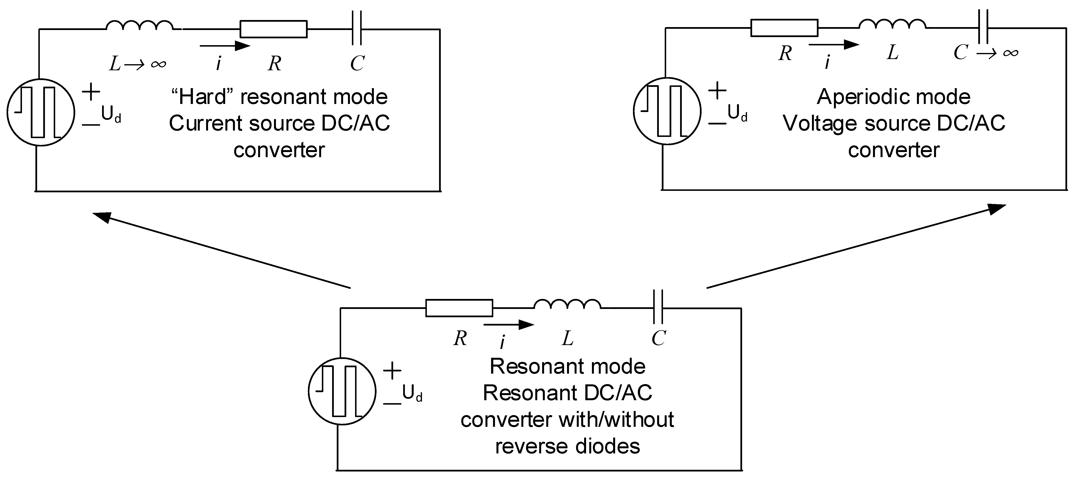
On the other hand, the RL circuit in the voltage source inverter can be represented as a series RLC circuit, with a capacitance value tending to infinity. As a result of these considerations and analogies, it can be concluded that the most general structure of DC/AC converters is a series RLC circuit, which under certain conditions operates in a resonant mode and under others—not. In this sense, it can be concluded that the resonant DC/AC converter represents the most general case, which summarizes and contains all possible operating modes, and the other types of inverters represent its special cases. The representation of the equivalent circuits of all types of DC/AC converters, as well as the transition between them, is shown in Figure 2.
It is characteristic of all types of DC/AC that, in their analysis, a series equivalent circuit of the AC circuit is used, which achieves a community of considerations. In this sense, the unified approach is based on the use of a series RLC circuit, which describes the electromagnetic processes in the resonant DC/AC inverter with reverse diodes. The other two main types of DC/AC converters are considered as special cases, respectively, with a resonant inductance tending to infinity (current source inverter) or a capacitor tending to infinity (in which case it is not possible to operate in resonance, but in aperiodic mode)—voltage source inverter.
When performing the analysis of resonant DC/AC converters, the following parameters are entered:
- -
- Coefficient of hesitation ;
- -
- Detuning factor of the equivalent AC circuit ,
Where is the resonant frequency of the series resonant circuit, is its attenuation, ω = 2πf is marked circular control frequency and —normalized to the control frequency conduction angle of the controllable semiconductor switches;
The use of coefficients k and ν is in the spirit of the traditions of the Department of “Power Electronics” at the Technical University of Sofia, Bulgaria, where they were introduced to carry out the analysis of resonant DC/AC converters [25,26]. On the other hand, with the definitions made in this way, the relationship between the coefficient k and the quality factor Q of the series resonant circuit is clearly defined and unambiguous:
When working in aperiodic mode, the following parameters used in the analysis of power electronic devices are introduced by analogy:
- -
- —coefficient of aperiodicity;
- -
- —quasi-frequency factor,
Where is quasi-resonant frequency.
3. Basic Ratios Used to Analyze DC/AC Converters
In this section, based on the analysis of the resonant DC/AC converter with reverse diodes, the expressions for the state variables—the inverter current and the capacitor voltage—will be found. All expressions will be obtained on the basis of the full-bridge scheme, and when working with other types of schemes (half-bridge, push-pull or mid-point of the transformer) there are derived numerical coefficients with which the results of the bridge scheme are adapted to these scheme varieties [23,26].
3.1. Analysis of a Resonant DC/AC Converter with Reverse Diodes
The scheme of a full-bridge resonant DC/AC converter is shown in Figure 1c. Characteristic of this topology is that, depending on the ratio between the parameters of the AC circuit, it is possible to operate in resonant or aperiodic mode. An analysis of the inverter was made assuming the ideality of all circuit elements.
The series RLC circuit under consideration is described by the following differential equation with respect to the capacitor voltage [16,22]:
where usw is the input voltage applied to the series circuit. It is formed by the sequential operation of the semiconductor switches (transistors and reverse diodes) of the inverter with a switching frequency f = 1/T.
When operating in an established mode and fulfilling the condition for resonance— the following expressions of the current through the inductance and the voltage of the capacitor are valid for the circuit under consideration [22,25,26]:
where IL(0) and UC(0) reflect the initial conditions in the circuit, R is the load resistance, L and C are the resonant inductance and resonant capacitor, Ud is the DC supply voltage.
Depending on the ratio between the control frequency and the resonance frequency of the serial RLC circuit, operating modes with a control frequency below and above the resonance are possible. Figure 3 shows the shape of the current through the inductance when operating with a control frequency below the resonance—Figure 3a and above the resonance Figure 3b. In the figure, the initial value of the current is marked, as well as its initial phase ψ.
When the device operates in an established mode, regardless of the ratio of the resonance and the control frequency, the conditions for the periodicity of the state variables are valid: and , and on this basis, their initial values are determined. On the other hand, the fact that the two state variables alternately change their signs at the beginning and at the end of the half-period of the driving frequency (shown for the current in Figure 3) allows unified expressions for both the under- and over-resonant driving frequency mode.
The initial current and voltage values are determined from the periodicity conditions:
where is a quantity characterizing the series RLC circuit, called the coefficient of variation in RLC resonant inverters with reverse diodes, and h and a are denoted as follows:
After substituting the initial current and voltage in (3), the inverter current and voltage of the resonant capacitor is obtained as follows:
where , , and and are the initial phases of the current through the resonant inductance and the voltage across the resonant capacitor, respectively.
In the further analysis of the scheme for a larger community of considerations, it is necessary to perform a normalization of the conduction angle of the semiconductor switches with respect to the control frequency ω, in which the expressions for iL(θ) and uC(θ) obtain the form:
where θ = ωt, , and .
In order to apply the unified approach to analysis and the representation from generalized positions of the processes in all basic schemes of DC/AC converters, it is appropriate to present the expression for the current from (6) as a function of the load in the following way:
After defining the state variables, in practice, the basic relationships for finding all the quantities necessary for the design of the power electronic device can be considered to have been found.
3.2. Current Source Inverter Analysis
Considerations of the current source inverter as a resonant inverter operating at a large ratio between the control frequency and the resonant frequency of the equivalent series AC circuit (values of the detuning factor greater than 3) are known [25,26,27]. For convenience, we will call the mode at such values of the detuning coefficient “hard” resonant, in contrast to the conditionally called “soft” resonant mode, where the difference between the two frequencies is a maximum of 20–30%. In practice, the parallel load circuit (Figure 1a) usually works in capacitive tuning and its equivalent first harmonic parameters, together with the input inductance, form a series resonant circuit. Due to the requirement for small input current ripple (to realize a current source type supply), the input inductance is usually assumed to be of a very large value, thus forming a very low value of the resonant frequency of the equivalent AC circuit. Figure 4 shows the shapes of the current in the AC circuit (iAC) and the voltage on the equivalent capacitor (uC) when operating in “hard” resonance mode.
In steady-state operation, the same equivalent circuit is present as in the case of the resonant inverter with reverse diodes, and thanks to the large value of the input inductance, the condition for resonance— is fulfilled even more strictly for the device under consideration, and therefore, the same expressions are valid (2) for the current through the inductance and the capacitor voltage [26]. The special thing is that the elements R and C of the series substitution scheme of an AC circuit are equivalent and represent the values of the active and reactive resistance according to the first harmonic of the parallel load circuit [27,28].
The peculiarities of the operating mode are reflected by the periodicity conditions, which, according to the time diagrams of Figure 4, are as follows: and . After substitution in the expressions for the current in the AC circuit and the capacitor voltage, we obtain the following equations for determining the initial conditions of the state variables in the case under consideration:
where is a quantity characterizing the series RLC circuit, called the coefficient of variation in current source inverters (resonant with “hard” commutation inverters) and hCS and aCS are denoted as follows:
After substituting the initial values of the state variables thus determined in (2), the inverter current and the voltage of the resonant capacitor are obtained as follows:
where , , and are the initial phases of the current through the resonant inductance and the voltage across the resonant capacitor, respectively.
In order to achieve greater universality of the considerations made, a normalization of the conducting angle of the semiconductor switches with respect to the control frequency ω was carried out, whereby the expressions for iL(θ) and uC(θ) obtain the form:
where and .
In order to achieve the unified approach for the analysis of the processes in all basic schemes of DC/AC converters, a conversion of the expression for the current from (10) was carried out, as it is presented as a function of the equivalent load:
One of the great advantages of viewing the current source inverter as a resonant, hard-switched mode is that it makes it possible to design a current inverter with a finite value of input inductance. In general, the problem of the optimal determination of the magnitude of the input inductance is fundamental from the point of view of the optimal design of current source inverters in general [2,27,28].
3.3. Analysis of a Resonant DC/AC Converter without Reverse Diodes
It is known that resonant DC/AC converters without reverse diodes can work in several operating modes, and unlike the previous case of a current source inverter, the control frequency is less than or at most equal to the resonant frequency [25,26,27]. In this case, the same equivalent circuit is used as in the previous case, but the current through the inductance has a zero initial value. This yields simplified expressions for the state variables versus expressions (3):
For the voltage on the equivalent capacitor, the condition of periodicity in the statutory regime is valid: . After substituting into the capacitor voltage expression for its initial condition, we obtain:
which is also the condition for defining the fluctuation coefficient.
UC(0) = (2k − 1)Ud,
After substituting the initial condition of the capacitor voltage, the expressions (11) obtain the form:
If a compact description is used to describe the capacitor voltage, then the state variables are defined by:
where , and is the initial phase of the voltage across the resonant capacitor.
After normalizing the conduction angle of the semiconductor switches with respect to the switching frequency ω, the expressions for iL(θ) and uC(θ) are:
where .
Accordingly, after expressing the state variables as functions of the equivalent load, it is obtained as follows:
Thus, after determining these quantities, all others can be found that serve to design the power circuit.
3.4. Analysis of a Series RLC Inverter Operating in Aperiodic Mode
This is one of the less common in practice, but it will be discussed in view of the fact that this mode is a generalization of the voltage source inverter case. In this case, the RLC inverter works in aperiodic mode, which corresponds to the fulfillment of the condition . In this variant, the state variables are defined as follows:
From the joint solution of (18) using the conditions for the periodicity of the current through the load and the capacitor voltage, i.e., and , the initial current and voltage values are determined:
where is a quantity characterizing the series RLC inverters with reverse diodes, called the aperiodicity coefficient, and hap and aap are denoted as follows:
After substituting the initial current and voltage in (18), the current through the inductance and the capacitor voltage is obtained as follows:
where , , and .
After normalizing the conduction angle of the transistors with respect to the control frequency ω, the expressions for iL(θ) and uC(θ) take the form:
where θ = ωt, , and .
3.5. Voltage Source Inverter Analysis
The above consideration of aperiodic mode operation of a series RLC inverter is the basis for the analysis of the stand-alone voltage source inverter. The innovative in this representation is the consideration of the voltage inverter as a special case of a series aperiodic RLC inverter with reverse diodes at capacitor value C = ∞ [29]. Thus, for the analysis of a voltage source inverter, the relations already determined can be used, noting that when C = ∞, then δ = Ω0.
In the analysis of a voltage inverter, the aperiodicity factor takes on a single fixed value = 1.045.
Then, the expression for the current through the inductance, represented by its initial phase, is:
where , , .
By normalizing with respect to the driving frequency ω, the expression for iL(θ) takes the form:
where θ = ωt, and .
In this way, it becomes possible to determine the current load of all circuit elements and their sizing with a view to achieving the parameters of the task and ensuring the expected operation of the device.
4. Verification of the Unified Analysis Approach
In this section, several computational examples of the design of different types of DC/AC converters are presented and the methods by which they are designed are based on the unified analysis approach. Certain elements of the unified approach, such as the representation of the current source inverter as a hard-switched resonant one, have been presented in [25].
To confirm the results achieved in the design of current inverters, computer simulations were made using the LTSPICE simulator and also verified on working power electronic devices with industrial applications.
Initial data for the design of a full-bridge current source inverter (Figure 1a) are:
- -
- output active power P = 100 kW;
- -
- load power factor cosφT = 0.15;
- -
- RMS value of loading voltage UOUT = 750 V;
- -
- output frequency f = 2400 Hz.
As a result of the design, the following values of the circuit elements were determined: RT = 0.12656 Ω, LT = 55.319 μH, C = 88.406 μF and L = 2.187 mH. For design purposes, a DC power supply value of 500 V was chosen.
Figure 5 shows the simulation results of the research of the designed DC/AC converter—parallel current source inverter. In sequence, from top to bottom, they are presented as follows: the input current (current through the inductance) Id, the output voltage (the voltage across the parallel capacitor C) UOUT and the voltage across the thyristor VS1—UVS1. The simulation model by which these results were obtained is given in Appendix A at the end of the paper. Since the simulator used lacks a thyristor model, it is replaced by a series circuit of a bipolar NPN transistor and a diode. In this way, a group is obtained that imitates the real action of the thyristor.
Table 1 compares the results calculated using the unified analysis and the current source inverter design methodology based on it with those obtained from the simulator and experiments. The values obtained from the simulation studies were determined using the basic functions of the computer simulator.
Data listed in Table 1 show that, for all values determined at design, errors are less than 2%.
The following computational example is based on the design of a transistor resonant inverter without reverse diodes (schematic of Figure 1b)
Initial data for the design of a full-bridge transistor resonant inverter are:
- -
- output active power P = 10 kW;
- -
- load power factor cosφT = 1;
- -
- RMS value of loading voltage UOUT = 270 V;
- -
- output frequency f = 50,000 Hz.
As a result of the design, the following values of the circuit elements were determined: R = 7.29 Ω, L = 33.178 μH and C = 272.1 nF. For design purposes, a DC power supply value of 300 V was chosen. Furthermore, a mode of operation with a control frequency equal to the resonant frequency of the series resonant circuit was selected.
Figure 6 shows the simulation results of the study of the designed DC/AC converter—series resonant inverter without reverse diodes. The input current (measured based on the absolute value of the current through the resonant inductance) Id and the output voltage (the voltage on the load)—UOUT are consecutively presented from top to bottom. The simulation model of the resonant inverter by which the presented results were obtained is given in Appendix A at the end of the paper.
Table 2 compares the results calculated using the unified analysis and the full-bridge resonant inverter without reverse diodes design methodology based on it with those obtained from the simulator and experiments.
Data listed in Table 2 show that, for all values determined at design, errors are less than 2%.
The next computational example is based on the design of a transistor resonant inverter with reverse diodes (schematic of Figure 1c)
Initial data for the design of a full-bridge transistor resonant inverter are:
- -
- output active power P = 10 kW;
- -
- load power factor cosφT = 1;
- -
- RMS value of loading voltage UOUT = 270 V;
- -
- output frequency f = 50,000 Hz.
Selected operating mode with a control frequency greater than the resonant frequency of the series resonant circuit—value of the detuning coefficient ν = 1.1.
As a result of the design, the following values of the circuit elements were determined: R = 7.29 Ω, L = 36.496 μH and C = 299.32 nF. For design purposes, a DC power supply value of 300 V was chosen.
Figure 7 shows the simulation results from the study of the designed DC/AC converter—series resonant inverter with reverse diodes. In sequence from top to bottom, the current consumed by the DC power source (formed by the sequential operation of transistors and reverse diodes) Id and the output voltage UOUT are presented. Characteristic of the considered power topology is that, during the conduction of the reverse diodes, energy is returned to the DC power source. For this reason, negative sections are observed in the form of the input current, which correspond to the release of energy from the AC circuit to the DC power source. The simulation model by which these results were obtained is given in Appendix A at the end of the paper.
Table 3 compares the results calculated using the unified analysis and the full-bridge resonant inverter with reverse diodes design methodology based on it with those obtained from the simulator and experiments.
Data listed in Table 3 show that for, all values determined at design, errors are less than 5%. The larger difference between the results of the design, simulations and experiments is due not to inaccuracies in the analysis, but to the fact that the design methodology is based on the application of the quasi-boundary method [22].
The last computational example is based on the design of a transistor voltage source inverter (schematic of Figure 1d)
Initial data for the design of a full-bridge transistor voltage source inverter are [29]:
- -
- total output power S = 1000 VA;
- -
- load power factor cosφT = 0.303;
- -
- RMS value of the first harmonic of the output voltage U(1) = 100 V;
- -
- output frequency f = 500 Hz.
As a result of the design, the following values of the circuit elements were determined: load resistance R = 3.033 Ω and load inductance L = 3.033 mH. For design purposes, a DC power supply value of 111 V was chosen.
Figure 8 shows the simulation results of the study of the designed DC/AC converter—voltage source inverter. In sequence from top to bottom, the current consumed by the DC power source (formed by the sequential operation of transistors and reverse diodes) Id and the output voltage UOUT are presented. For this power topology, during the conduction of the reverse diodes, energy is returned to the DC power source. The RMS of the first harmonic of the output voltage is found by performing harmonic analysis. The simulation model by which these results were obtained is given in Appendix A at the end of the paper.
Table 4 compares the results calculated using the unified analysis and the full-bridge voltage source inverter design methodology based on it with those obtained from the simulator and experiments.
Data listed in Table 4 show that, for all values determined at design, errors are less than 1%.
5. Discussion and Conclusions
From the analysis and comparison of the results obtained in the design of the main types of DC/AC converters using design methods based on the unified analysis approach and those from computer simulations and prototypes, it was found that a very good accuracy is achieved—a difference of less than 5%. In this way, not only the applicability, but also the rationality and effectiveness of the new analysis approach are proven, apart from the positions of the theory of electric circuits and electrical engineering, but also on the basis of various experiments. The main advantage of the proposed unified approach is that, unlike other analysis methods, it describes the current through the AC circuit in its actual form. In this sense, it approaches the exact analyses that are based on a description of the electromagnetic processes in the power circuit with systems of differential equations.
In essence, the unified analysis approach is a development and generalization of the theory of autonomous inverters. On the other hand, the derived ratios, in which the influence of the active resistance of the AC circuit is also taken into account, make an assessment regarding the influence of the change of the circuit parameters on the operating modes. A major drawback of the unified approach is that it does not cover the DC/AC converters that inject energy into the power grid and are widely used in decentralized power generation systems.
On the other hand, the definition and development of the unified approach in the analysis of the three main types of DC/AC converters leads to a community of results, to an easier and more convenient comparison of their characteristics and, last but not least, to the creation of unified engineering methodologies for their design. Combining these methods with artificial intelligence techniques (mostly the application of different optimization procedures) is one of the guidelines for the future application and development of the unified approach. The main idea of this approach is based on the achievements of computational mathematics and the application of mathematical software to speed up and improve the design process of power electronic devices and systems, and to guarantee their performance taking into account the tolerances of circuit elements and the presence of various disturbing effects. The proposed analysis approach is also applicable to three-phase DC/AC inverters, taking into account the specifics related to the presence of three phases and, accordingly, their mutual influence in the formation of the output currents and voltages.
The application of the unified approach in the analysis, combined with normalization by the control frequency of the conduction angle of the semiconductor devices, is also useful from a methodological point of view for the needs of training in power electronics. In this aspect, considering the current source inverter as a resonant operating in hard commutation mode enables the accurate design of current source inverters with a finite value of input inductance. In this sense, the unified analysis approach solves one of the big problems in prototyping a whole class of power electronic devices with industrial application.
Funding
This research was funded by Bulgarian National Scientific Fund, grant number KII-06-H57/7/16.11.2021, and the APC was funded by KII-06-H57/7/16.11.2021.
Acknowledgments
This research was carried out within the framework of the project “Artificial Intelligence-Based modeling, design, control and operation of power electronic devices and systems”, KII-06-H57/7/16.11.2021, Bulgarian National Scientific Fund.
Conflicts of Interest
The author declare no conflict of interest.
Nomenclature
| Q | quality factor of the equivalent series resonant AC circuit |
| k | coefficient of hesitation of a series resonant circuit |
| ν | detuning factor of the equivalent series resonant AC circuit |
| ω0 | resonant frequency of the equivalent series resonant AC circuit |
| ω | control frequency, switching frequency |
| δ | attenuation of the equivalent series resonant AC circuit |
| λ | normalized to the control frequency conduction angle of the controllable semiconductor switches |
| kA | coefficient of aperiodicity of a serial RLC circuit |
| νA | quasi-frequency factor |
| Ω0 | quasi-resonant frequency of a serial RLC circuit |
| IL(0) | initial condition for the current through the inductance |
| UC(0) | initial condition for the capacitor voltage |
| Ud | DC supply voltage. |
| K | coefficient of variation in RLC resonant inverters with reverse diodes |
| ψ | initial phase of the current through the resonant inductance |
| φ | initial phase of the voltage across the resonant capacitor |
| KCS | coefficient of variation in current source inverters (resonant with “hard” commutation inverters) |
| Kap | coefficient of aperiodicity of series RLC inverters with reverse diodes |
| tq | schematic recovery time of thyristors |
Appendix A
The simulation models of the designed DC/AC converters are presented in the Appendix A. The graphical and numerical results presented in the manuscript were obtained through these models. Figure A1 shows the simulation model of a parallel current source inverter. As already commented, due to the absence of thyristors in the standard semiconductor element model libraries in the used simulator, a series connection of a bipolar NPN transistor and a diode is used in the simulation studies.
Figure A1.
Simulation model of parallel current source inverter.

Figure A2 shows the simulation model of a series resonant inverter without reverse diodes.
Figure A2.
Simulation model of a series resonant inverter without reverse diodes.

Figure A3 shows the simulation model of a series resonant inverter with reverse diodes.
Figure A3.
Simulation model of a series resonant inverter with reverse diodes.

Figure A4 shows the simulation model of a voltage source inverter.
Figure A4.
Simulation model of a voltage source inverter.

References
- Ned Mohan, U.; Tore, M.; Robbins; William, P. Power Electronics—Converters, Applications, and Design, 3rd ed.; John Wiley & Sons: Hoboken, NJ, USA, 2003. [Google Scholar]
- Zinoviev, G. Fundamentals of Power Electronics—Part II; Novosibirsk State University: Novosibirsk, Russia, 2004. (In Russian) [Google Scholar]
- Rashid, M.H. Power Electronics Handbook: Devices, Circuits, and Applications; Academic Press: Cambridge, MA, USA, 2007. [Google Scholar]
- Erickson, R.W.; Maksimovic, D. Fundamentals of Power Electronics, 2nd ed.; Kluwer Academic Publishers Group: Bonn, Germany, 2001. [Google Scholar]
- Yang, X.; Zhao, Z.; Wang, C.; Xu, J.; Liu, K.; Qiu, J. Analysis and Parameter Design of SiC-Based Current Source Inverter (CSI). World Electr. Veh. J. 2022, 13, 187. [Google Scholar] [CrossRef]
- Mauricio, J.M.; Torres, M.; Baier, C.; Silva, J. Enhanced average model for current source converter hybrid simulations. In Proceedings of the IEEE International Conference on Industrial Technology (ICIT), Seville, Spain, 17–19 March 2015; pp. 2520–2525. [Google Scholar] [CrossRef]
- Combe, Q.; Pierfederici, S.; Weber, M.; Dufour, S. Modeling, Analysis and Control of Current Source Converter. In Proceedings of the IECON 2021—47th Annual Conference of the IEEE Industrial Electronics Society, Toronto, ON, Canada, 13–16 October 2021; pp. 1–6. [Google Scholar] [CrossRef]
- Wang, H.; Saha, T.; Riar, B.; Zane, R. Design Considerations for Current-Regulated Series-Resonant Converters With a Constant Input Current. IEEE Trans. Power Electron. 2019, 34, 141–150. [Google Scholar] [CrossRef]
- Vishnuram, P.; Ramachandiran, G.; Sudhakar Babu, T.; Nastasi, B. Induction Heating in Domestic Cooking and Industrial Melting Applications: A Systematic Review on Modelling, Converter Topologies and Control Schemes. Energies 2021, 14, 6634. [Google Scholar] [CrossRef]
- Dokić, B.L.; Blanuša, B. Power Electronics Converters and Regulators, 3rd ed.; Springer International Publishing: Cham, Switzerland, 2015; ISBN 978-3-319-09401-4. [Google Scholar]
- Khluabwannarat, P.; Thammarat, C.; Tadsuan, S.; Bunjongjit, S. An analysis of iron loss supplied by sinusoidal, square wave, bipolar PWM inverter and unipolar PWM inverter. In Proceedings of the 2007 International Power Engineering Conference (IPEC 2007), Singapore, 3–6 December 2007; pp. 1185–1190. [Google Scholar]
- Lian, R.K.-L.; Subroto, R.K.; Andrean, V.; Lin, B.H. Modeling of Voltage Source Converters. In Harmonic Modeling of Voltage Source Converters Using Basic Numerical Methods; IEEE: Piscataway, NJ, USA, 2022; pp. 95–147. [Google Scholar] [CrossRef]
- Kharjule, S. Voltage source inverter. In Proceedings of the 2015 International Conference on Energy Systems and Applications, Pune, India, 30 October–1 November 2015; pp. 537–542. [Google Scholar] [CrossRef]
- Popov, E. Analysis, Modeling and Design of Converter Units (Computer—Aided Design of Power Electronic Circuits); Technical University Printing House: Sofia, Bulgaria, 2005. (In Bulgaria) [Google Scholar]
- Penev, D.; Arnaudov, D.; Hinov, N. Formalization, Equivalence and Generalization of Basic Resonance Electrical Circuits. In Proceedings of the AIP Conference Proceedings, Sozopol, Bulgaria, 8–13 June 2017; Volume 1910, ISBN 978-0-7354-1602-4. [Google Scholar] [CrossRef] [Green Version]
- Kazimierczuk, M.K.; Czarkowski, D. Resonant Power Converters, 2nd ed.; IEEE Press and John Wiley & Sons: New York, NY, USA, 2011; pp. 1–595. ISBN 978-0-470-90538-8. [Google Scholar]
- Cutrona, C.; Di Miceli, C. A unified approach to series, parallel and series-parallel resonant converters. In Proceedings of the Telecommunications Energy Conference, INTELEC ’92, Washington, DC, USA, 4–8 October 1992; pp. 139–146. [Google Scholar]
- Ivensky, G.; Zeltser, I.; Kats, A.; Ben-Yaakov, S. Reducing IGBT Losses in ZCS Series Resonant Converters. IEEE Trans. Ind. Electron. 1999, 46, 67–74. [Google Scholar] [CrossRef]
- Mikhalchenko, S.G.; Stolyarova, A.A. Analysis of resonant converters at wide input voltage range. In Proceedings of the 2016 17th International Conference of Young Specialists on Micro/Nanotechnologies and Electron Devices (EDM), Erlagol, Altai, Russia, 30 June–4 July 2016; pp. 512–517. [Google Scholar] [CrossRef]
- Song, Z.; Gao, Y.; Shang, P. Parameter Design Method of a Series-parallel Resonant Converter. In Proceedings of the 2018 IEEE 4th Information Technology and Mechatronics Engineering Conference (ITOEC), Chongqing, China, 14–16 December 2018; pp. 1024–1027. [Google Scholar] [CrossRef]
- Steigerwald, R.L. Practical design methodologies for load resonant converters operating above resonance. In Proceedings of the Fourteenth International Telecommunications Energy Conference—INTELEC ’92, Washington, DC, USA, 4–8 October 1992; pp. 172–179. [Google Scholar] [CrossRef]
- Hinov, N. Quasi-Boundary Method for Design Consideration of Resonant DC-DC Converters. Energies 2021, 14, 6153. [Google Scholar] [CrossRef]
- Todorov, T.S.; Madzharov, N.D.; Alexiev, D.T.; Ivanov, P.T. Autonomous Inverters; Technical University of Gabrovo: Gabrovo, Bulgaria, 1996. [Google Scholar]
- Madzharov, N. High-frequency power source with constant output power. J. Eng. Sci. Technol. Rev. 2016, 9, 157–162. [Google Scholar] [CrossRef]
- Hinov, N.L. Power Converters of Electrical Energy with Industrial Application. Ph.D. Thesis, Technical University, Sofia, Bulgaria, 1998. (In Bulgaria). [Google Scholar]
- Gradinarov, N.P. Analysis and Development of Autonomous Resonant Inverters with Electrical Application. Ph.D. Thesis, Technical University of Sofia, Sofia, Bulgaria, 2002. (In Bulgarian). [Google Scholar]
- Berkovich, E.I.; Ivenskyi, G.V.; Joffe, Y.S.; Matchak, A.T.; Morgun, V.V. High-Frequency Thyristor Converters for Electrical Devices; Energoatomizdat: Leningrad, Russia, 1983. (In Russian) [Google Scholar]
- Dede, E.; Espi, J.; Esteve, V.; Jordan, J.; Casans, S. Trends in Converters for Induction Heating Applications. In Proceedings of the Thirty-Fifth International Intelligent Motion Conference, Nürnberg, Germany, 22–24 June 1999; pp. 155–160. [Google Scholar]
- Hinov, N. New Method for Analysis and Design Consideration of Voltage Source Inverters. Energies 2022, 15, 3695. [Google Scholar] [CrossRef]
Figure 1.
Full-bridge power schemes of DC/AC converters. (a) Parallel current source inverter; (b) series resonant DC/AC converter; (c) resonant DC/AC converter with reverse diodes; (d) voltage source inverter.
Figure 1.
Full-bridge power schemes of DC/AC converters. (a) Parallel current source inverter; (b) series resonant DC/AC converter; (c) resonant DC/AC converter with reverse diodes; (d) voltage source inverter.


Figure 2.
Generalized equivalent circuits of the three main types of DC/AC converters and the transition between them.
Figure 2.
Generalized equivalent circuits of the three main types of DC/AC converters and the transition between them.

Figure 3.
Steady State Inductance Current Shape of a Resonant DC/AC Converter with Reverse Diodes: (a) with a control frequency below resonance; (b) with a control frequency above resonance.
Figure 3.
Steady State Inductance Current Shape of a Resonant DC/AC Converter with Reverse Diodes: (a) with a control frequency below resonance; (b) with a control frequency above resonance.

Figure 4.
Time diagram of the current in the AC circuit and the voltage on the equivalent series capacitor in a current source inverter.
Figure 4.
Time diagram of the current in the AC circuit and the voltage on the equivalent series capacitor in a current source inverter.

Figure 5.
Time diagram of the input current—Id, output voltage—uOUT and voltage across thyristor VS1—uVS1 in the designed and simulated current source inverter.
Figure 5.
Time diagram of the input current—Id, output voltage—uOUT and voltage across thyristor VS1—uVS1 in the designed and simulated current source inverter.

Figure 6.
Time diagram of the input current—Id and output voltage—uOUT.

Figure 7.
Time diagram of the input current—Id and output voltage—uOUT.

Figure 8.
Time diagram of the input current—Id and output voltage—uOUT.


Table 1.
Output data and obtained results from simulation and experiment for full-bridge current source inverter.
Table 1.
Output data and obtained results from simulation and experiment for full-bridge current source inverter.
| Intput Data | Computer Simulation | Experiment |
|---|---|---|
| UOUT, V = 750 | 738.15 | 746.25 |
| Id, A = 200 | 199.45 | 195.2 |
| tq, μs = 49 | 48.874 | 48.7 |
Table 2.
Output data and obtained results from simulation and experiment for full-bridge transistor resonant inverter without reverse diodes.
Table 2.
Output data and obtained results from simulation and experiment for full-bridge transistor resonant inverter without reverse diodes.
| Intput Data | Computer Simulation | Experiment |
|---|---|---|
| UOUT, V = 270 | 266.61 | 267.25 |
| Id, A = 33.333 | 32.582 | 33.12 |
Table 3.
Output data and obtained results from simulation and experiment for full-bridge transistor resonant inverter with reverse diodes.
Table 3.
Output data and obtained results from simulation and experiment for full-bridge transistor resonant inverter with reverse diodes.
| Intput Data | Computer Simulation | Experiment |
|---|---|---|
| UOUT, V = 270 | 268.73 | 267.45 |
| Id, A = 33.333 | 33.097 | 32.9 |
Table 4.
Values of quantities obtained from the design of a voltage source inverter and the results of computer simulations and experiment.
Table 4.
Values of quantities obtained from the design of a voltage source inverter and the results of computer simulations and experiment.
| Intput Data | Computer Simulation | Experiment |
|---|---|---|
| U(1), V = 100 | 99.99 | 99.45 |
| I, A = 10 | 10.064 | 9.95 |
Disclaimer/Publisher’s Note: The statements, opinions and data contained in all publications are solely those of the individual author(s) and contributor(s) and not of MDPI and/or the editor(s). MDPI and/or the editor(s) disclaim responsibility for any injury to people or property resulting from any ideas, methods, instructions or products referred to in the content. |
© 2023 by the author. Licensee MDPI, Basel, Switzerland. This article is an open access article distributed under the terms and conditions of the Creative Commons Attribution (CC BY) license (https://creativecommons.org/licenses/by/4.0/).
Share and Cite
MDPI and ACS Style
Hinov, N. A Unified Approach to the Analysis of DC/AC Converters, Based on the Study of Electromagnetic Processes in a Series RLC Circuit. Electronics 2023, 12, 983. https://doi.org/10.3390/electronics12040983
AMA Style
Hinov N. A Unified Approach to the Analysis of DC/AC Converters, Based on the Study of Electromagnetic Processes in a Series RLC Circuit. Electronics. 2023; 12(4):983. https://doi.org/10.3390/electronics12040983
Chicago/Turabian StyleHinov, Nikolay. 2023. "A Unified Approach to the Analysis of DC/AC Converters, Based on the Study of Electromagnetic Processes in a Series RLC Circuit" Electronics 12, no. 4: 983. https://doi.org/10.3390/electronics12040983
Note that from the first issue of 2016, this journal uses article numbers instead of page numbers. See further details here.