Article

Analyzing Power Losses and Performance of an Isolated DC-DC Converter for Renewable Energies Systems

by
Jorge Ortíz-Marín
1,
Diego Gallo-Reyes
1,
Dante Ruiz-Robles
2,* and
Vicente Venegas-Rebollar
1
1
Programa de Graduados e Investigación en Ingeniería Eléctrica (PGIIE), Tecnológico Nacional de México/Instituto Tecnológico de Morelia, Morelia 58120, Mexico
2
Escuela Nacional de Estudios Superiores Unidad Juriquilla, Universidad Nacional Autónoma de México, Querétaro 76230, Mexico
*
Author to whom correspondence should be addressed.
Electronics 2023, 12(5), 1110; https://doi.org/10.3390/electronics12051110
Submission received: 11 January 2023 / Revised: 12 February 2023 / Accepted: 13 February 2023 / Published: 24 February 2023

Abstract

:
DC-DC converters are essential in the interconnection of photovoltaic (PV) systems and systems that operate at different voltages, frequencies, and powers, such as smart grids. Due to the energy transition, and therefore the need for high efficiency in PV systems and smart grids, there is a great challenge to develop DC-DC converters with the highest possible efficiency. Therefore, in this paper an isolated DC-DC converter with high efficiency and easy implementation is developed, in comparison with other similar structures. In isolated converters it is necessary to address the analysis and design of the transformer. Poor performance of this element can contribute to high losses and low efficiency of the converter topology. This study proposes an isolated DC-DC converter (FBDC) that operates at different levels of harmonic content in its supply. The design is subjected to two levels (2L) and three levels (3L), which affects the THD value. The proposed converter model is simulated in MATLAB-Simulink and validated in a laboratory prototype. Finally, the prototype is incorporated into the multilevel FBDC topology, obtaining an efficiency of 96.6% for 2L and 97.0% for 3L in the laboratory, showing the high performance of the proposed design.

Graphical Abstract

1. Introduction

Current electrical networks are facing new operation schemes due to the integration of energy generation and storage systems. These technologies are mainly wind generators [1], photovoltaic (PV) systems [2,3], electric vehicles (EV) [4], fuel cells [5], and batteries [6], also found in DC microgrid and rail systems [7]. Therefore, it is essential to have low-cost and high-efficiency linkage topologies [8]. Consequently, it is necessary to develop DC-DC converters that operate efficiently and reliably.
DC-DC converters are classified according to their operation as unidirectional and bidirectional and frequently are also divided as isolated and non-isolated [9]. In isolated converters, the transformer integrates galvanic isolation and transformation ratio operating as the central key element. Non-isolated converters are generally composed of more minor elements, making the topology more straightforward [10,11].
Transformers are grouped according to their operating frequency into (1) low-frequency transformers (LFT), (2) medium frequency transformers (MFT), and (3) high-frequency transformers (HFT). Isolated DC-DC converters commonly include MFTs and HFTs. This range of values is considered since the size of the transformer is inversely proportional to its operating frequency. Therefore, the higher the operating frequency, the lower the size and cost of the transformer.
The core materials commonly used in transformers are silicon steel, amorphous, nanocrystalline, and ferrite [12,13,14]. Due to their excellent performance and low cost, ferrite cores are applied in high-frequency operating converters. Amorphous and nanocrystalline materials have similar permeability values at a medium frequency (1–20 kHz). Despite this, nanocrystalline materials are gaining importance in their application inside converters due to their high saturation flux density, high permeability, and low operating losses. The material commonly used in LFT is silicon steel. However, for applications with a frequency of 1–5 kHz, a high-power density is not reported due to the low saturation flux density.
Related to the design and construction of medium-frequency transformers [15], presented a single-phase nanocrystalline core prototype. The methodology allowed MFT efficiencies in the design, simulation, and prototype stages of 99.23%, 99.28%, and 99.41%, respectively. The above demonstrates the effectiveness of the design and prototype used in the DAB converter. Similarly, a comparative design study is presented in [16], where two MFTs with different cores, one nanocrystalline and the other ferrite, are described. The design considers operating at 20 kHz, and the core has toroidal geometry. The resulting efficiencies are 99.8% for the nanocrystalline core prototype and 99.7% for the ferrite. However, in [15,16], the final value of the conversion efficiency is not presented, nor is there any mention of the impact that a multilevel signal generates on the transformer’s operation, reliability, and efficiency.
The number of levels in the transformer feed determines whether the topology is 2L or multilevel. The most popular multilevel topologies are neutral-point clamped (NPC), flying capacitor (FC), and cascaded H-bridge (CHB). In multilevel topologies, the THD value of the voltage decreases as the number of levels increases since the waveform resembles a sinusoidal signal. On the contrary, if the number of levels increases, the number of components in the topology also increases [17].
DAB is a bidirectional topology gaining attention due to modularity, galvanic isolation, and lossless switching. The transformer forms the central stage of the DAB, and at each end, there is a full-bridge (FB), which is responsible for rectifying or inverting the supply voltage. The modulation strategies are SPS (single phase-shift), EPS (extended phase-shift), DPS (dual phase-shift), and TPS (triple phase-shift) [18]. The SPS strategy induces 2L signals at both ends of the transformer. For EPS modulation, one signal is 3L, and the other is 2L, subjecting the transformer to different levels of total harmonic distortion (THD) in its supply. In the DPS modulation case, 3L signals are presented with identical THD at extremes. Finally, the TPS modulation originates signals of 3L with different THD. Each modulation presents advantages in specific applications for the DAB. However, the central element must guarantee reliability in all power conditions. An important advance of the DAB is presented in [19]; an FB is replaced by a five-level NPC, generating a multilevel DAB. In the investigation, the design of the HFT is considered; it uses an amorphous core and reaches an efficiency of 93%, and the final efficiency of the converter is 88%.
The isolated DC-DC topologies of the phase shift full-bridge (PSFB) and 3L DC-DC converter (TL-DC) feature constant updates in unidirectional applications. These topologies comprise the active stage, galvanic isolation (transformer), and rectification. In the same way as in DAB, for PSFB and TL-DC, the transformer is the central element, and it feeds with different THD levels. In [20], a PSFB is presented that integrates active elements between the source and the FB. The control strategy optimizes the conduction losses in the active elements, reaching an efficiency of 95.8% for the converter. The secondary winding is divided into four parts, each connected to a rectifying diode. For the PSFB presented in [21], the HFT contains a ferrite core, and an external leakage inductance is designed to improve the converter’s efficiency, reporting a value of 95.24%. In the case of [22], the TL-DC topology compares the operation and performance of the converter when the transformer is fed with 2L and 5L. It is concluded that increasing the number of levels increases the converter’s efficiency. Similarly, in [23,24], an NPC and anchored capacitors are integrated into the active stage of the topology, generating 5L; the contribution focuses on the control strategy and loss reduction, reporting 93.8% and 93.3% in the converters, respectively.
A dual half-bridge (DHB) topology is presented in [25], where the transformers that make up the topology are designed considering efficiency and power density. Ferrite cores operate in the high-medium frequency range; the efficiency of the transformers is 98%, and the converter reaches 95%. Although in [19,25], the design of the transformers that make up the multilevel topology is considered, it is not considered a detailed model. Similarly, the models that describe the transformer in [20,21,26,27,28] are limited since only some details of its behavior are integrated.
Unidirectional and bidirectional isolated topologies subject the transformer to different levels of THD. With the above, the equipment reaches operating points where its efficiency and reliability are greatly affected. Therefore, it is necessary to determine a design methodology for the transformer that guarantees reliability and high efficiency operated in new multilevel DC-DC topologies.
Based on transformer design methodologies [14,15,29], this research presents a design methodology that considers the parameters and updates that, from the authors’ point of view, are necessary to achieve and maintain high efficiency with different levels of THD in the prototype feed. The design characteristics are the number of turns in the windings, transformation ratio, core sizing, insulation, temperature, and medium frequency.
In this article, a high-power DC-DC converter with high voltage gain and high efficiency is introduced. It is a simple to implement structure (FBDC), with the characteristic of the use of new medium frequency transformers with nanocrystalline cores, silicon carbide MOSFETs and silicon carbide diodes. Among its main characteristics are:
(1)
Easy implementation.
(2)
The individual losses in each element (passive, active and transformer semiconductors) were considered.
(3)
Low-loss, high-efficiency DC-DC converter.
(4)
Isolated DC-DC converter.
(5)
DC-DC converter subjected to different THD values in the central stage (MFT).
(6)
Validation in simulation and laboratory.
This article is organized as described below: Section 2 explains the transformer design methodology and upgrades and the FBDC topology and loss calculation. Section 3 analyses the behavior of the transformer model in simulation, and then the prototype is verified in the laboratory within the FBDC topology. In Section 4, a discussion is presented. Finally, the conclusions are addressed in Section 5.

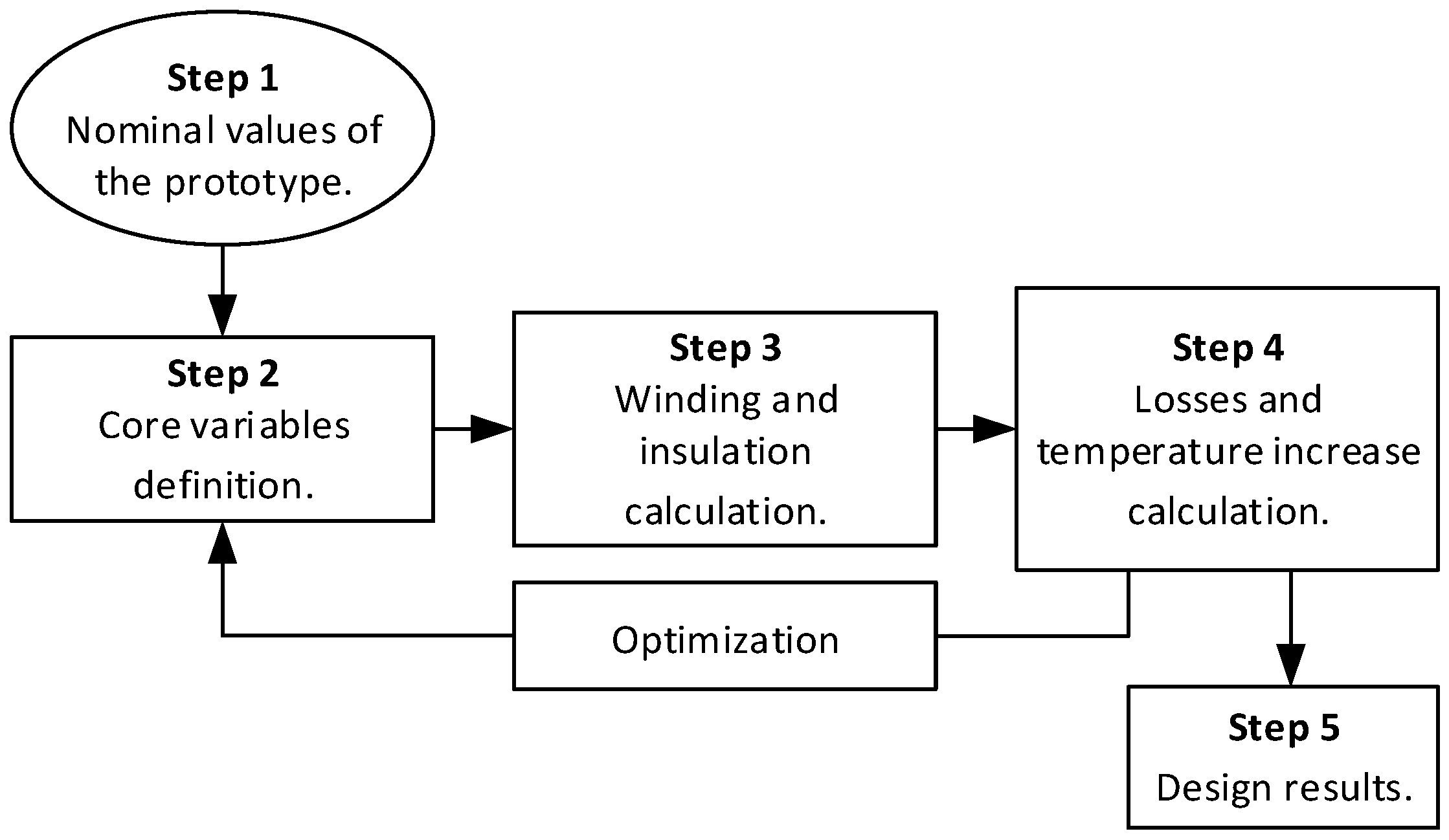
2. MFT Design Methodology with 2L and 3L Feeding

The development of design methodologies for transformers operating in medium frequency is under constant development. The contribution areas in the design focus on efficiency, core losses, temperature calculation, cost, and power density of the prototype [12,14,16]. Each methodology presents progress; however, the behavior of a multilevel power supply on the design is not addressed. Thus, this research proposes to address this effect and to design a reliable and efficient element that considers multilevels.
The design methodology described in this research considers the core geometry, insulation, conductor, losses, and operating temperature. The goals are to achieve high efficiency and reliability; hence the methodology described in [15] is taken as a basis; however, it is necessary to integrate the corresponding updates that ensure good performance with different THD in its power supply. Figure 1 shows the flow diagram of the proposed design methodology.
The design methodology comprises five steps, and the necessary upgrades are integrated to ensure the proper prototype operation with a multilevel power supply. As a first step, the nominal values of the prototype, input and output voltage (V1 and V2), output current (I2), frequency (f), current density (J), transformation ratio (n), waveform coefficient (Kf), window utilization factor (Ku) and output power (Pout) are chosen. In this stage, the peak supply voltage (V1_p and V2_p) is considered, i.e., the highest instantaneous values. The prototype can lose reliability, operate inefficiently, and present core saturation if the operating voltage is too high. For single-phase transformers, when the power supply signal is 2L, the RMS value equals the peak voltage value. On the other hand, when a multilevel power supply is present, the RMS value is lower than the peak voltage, and the performance of the transformer is thus degraded.
The core characteristics, such as material and geometry, are defined in the second step. The nanocrystalline material integrates high saturation flux density, high permeability, and low operating losses to the prototype and achieves good mid-frequency performance [12,15,16]. The toroidal geometry represents lower flux dispersion, so a combination of nanocrystalline material and toroidal geometry is the selected proposal in this research. The toroidal geometry is presented in Figure 2. The core dimensions considered in the design are outer diameter (OD), inner diameter (ID), core length (HT), window area (Wa), effective core cross-section (Ac), and the area product (Ap). The design process considers the nominal (Bac) and maximum (Bmax) flux density, where Bmax is the core saturation value. The maximum value of flux density is presented when the prototype operates with multilevel feed, so it is the value considered as nominal flux density, thus covering the operation with multilevel feed, assuring the correct operation with 2L feed.
In the third step, the winding and insulation characteristics are defined. This includes the number of turns of the primary and secondary (Np and Ns), the area of the primary and secondary conductor (Awp and Aws), rated primary current (I1), the minimum distance between conductors (dins), required insulation voltage (Uins), insulation dielectric strength (Eins) and safety margin (v). The insulation distance between the windings (Dps) is determined, as well as the minimum insulation distance of the primary (Dp) and secondary (Ds) conductors. The conductors usually used in transformer construction are flat conductors, Litz wire, and solid conductors. For this research, the conductor used is solid round copper due to its good performance in MFTs. The number of turns of the primary is calculated with Equation (1). The rated current and current density define the conductor size using Equation (2). The minimum distance between the primary, secondary, and windings conductors is determined by applying Equation (3).
N p = V 1   · 10 4 B a c · f · K f · A c
A w p = I 1   J
d i n s = U i n s   v · E i n s
The fourth step is dedicated to calculating the efficiency of the MFT and the temperature rise. The primary winding resistance (R1) and secondary winding resistance (R2) are calculated using Equation (4). The primary and secondary winding losses (Pp,s) and copper losses (Pcu) are estimated with Equation (5). The magnetization inductance (Lm) and leakage inductance (Ld) are also calculated, and the equivalent model of the transformer is defined in [15]:
R 1 , 2 = M L T ( N p , s ) ( μ Ω c m 1 , 2 ) × 10 6
P c u = I 1 2 · R 1 + I 2 2 · R 2
where MLT corresponds to the average distance of each winding turn, µΩ/cm1 and µΩ/cm2 are the resistances per centimeter of the primary and secondary winding conductors.
The core losses (Pfe) are determined by Equation (6), where Wfe is the core weight in kg. The manufacturer provided the losses in nanocrystalline material (Pfe_core); for 20 kHz, which is equivalent to 40 W/kg [30]. The total losses (Ptot) in the MFT are estimated with Equation (7), and by applying Equation (9), the MFT efficiency is calculated.
P f e = P f e   _ c o r e · W f e
P t o t = P c u + P f e
P o u t _ M F T = P i n _ M F T P t o t
E f f M F T = P o u t _ M F T P i n _ M F T · 100 %
At this design stage, two optimization conditions are integrated. The first corresponds to the temperature rise (Tr) calculation, where a maximum operating temperature of 80 °C is considered. This condition ensures an operating margin for the core since the maximum temperature for the nanocrystalline material is 120 °C. The second condition is the final efficiency of the prototype, which must exceed 98%. Both conditions must be met to generate the result. Otherwise, the iterative calculation process resized the core, and steps two to four are repeated. Finally, step five presents the design results, which are: core dimensions (Wa, Ac, Ap), winding characteristics (Np, Ns, Awp, Aws), and insulation characteristics (Dps, Dp, Ds).

2.1. Multilevel Topologies

The multilevel topologies NPC, FC, and CHB present a linear increase of their elements concerning the number of levels (n) [31,32]. The number of diodes (d) in the NPC topology is calculated with Equation (10). The floating capacitors (fc) required in FC are determined with Equation (11). On the other hand, applying Equation (12), the source (p) for each bridge in the CHB topology is estimated. Finally, the number of switches in multilevel (sw) topologies is calculated using Equation (13).
d = ( n 1 ) ( n 2 )
f c = ( n 1 ) ( n 2 ) 2
p = n 1 2
s w = 2 ( n 1 )

2.2. Full-Bridge Converter (FBDC)

The FBDC topology is an isolated DC-DC unidirectional topology composed of three stages, the full-bridge (FB), the MFT, and the rectifier-bridge (RB). This topology, as with other multilevel, feeds the transformer with 2L and 3L signals at different points of operation; therefore, the transformer operates with different THD values using the same number of semiconductors. The FBDC diagram is shown in Figure 3.
The modulation generates 2L and 3L signals in Figure 4 to feed the transformer. Figure 4a presents the 2L modulation. The main signals S1 and S - 2 are 180° out of phase with the S3 and S - 4 . Figure 4b shows the modulation for 3L, where the signal applied to S1 and S - 2 is 45° out of phase with S4 and S - 3 . All modulation signals operate at nominal frequency and 50% duty cycle. The modulation in the FBDC to generate 2L and 3L show its simplicity, compared to other multilevel topologies with the same THD value [19,22,23,24,27,28].

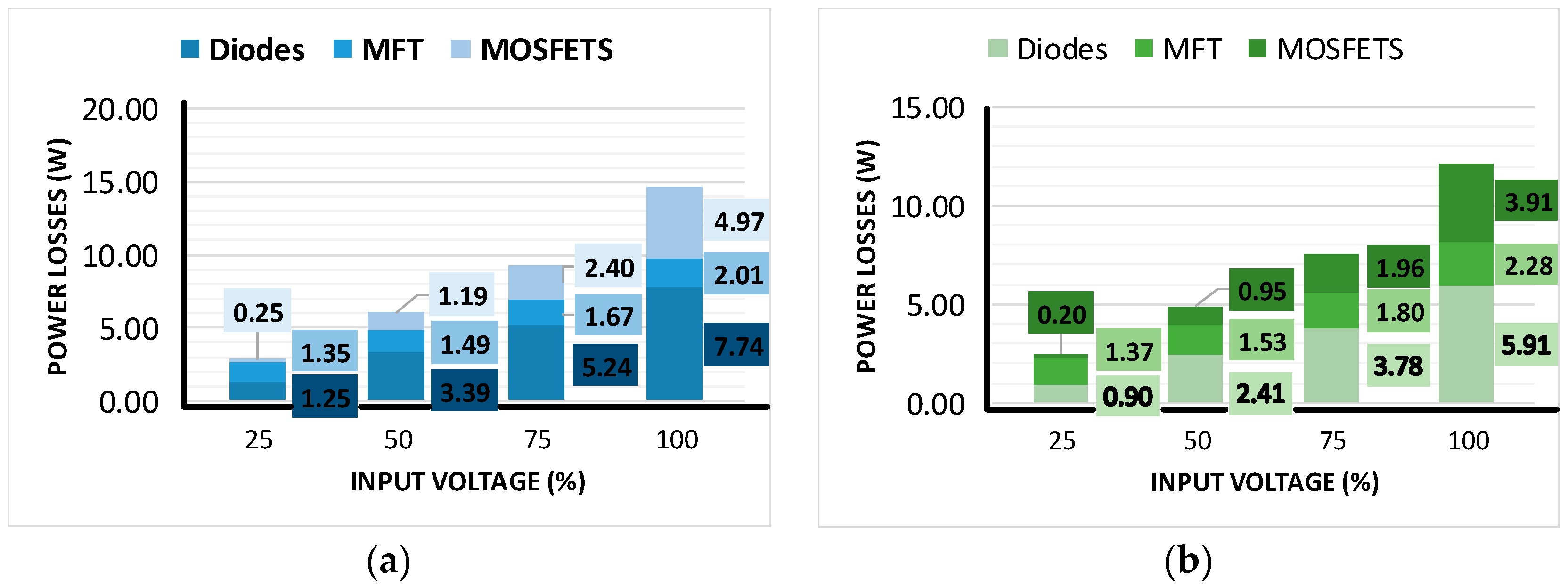
2.3. Estimation of Semiconductors Losses

Losses in active semiconductors are determined with Equation (14), and losses in the diodes are calculated with Equation (18) [33].
P M O S F E T = ( I D ( R M S ) 2 · R D S ( O N ) ) + P O N + P O F F
I D ( R M S ) = I D ( O N ) · D
P O N = f s w · I D ( O N ) · V D D · t O N · 1 2
P O F F = f s w · I D ( O N ) · V D D · t O F F · 1 2
P D I O D E = ( V F · I F ( A V G ) ) + ( I F ( R M S ) 2 · R D ( O N ) )
I F ( A V G ) = I M A X + I M I N 2 · δ
I F ( R M S ) = I M A X 2 + I M I N 2 + ( I M A X · I M I N ) 3 · δ
where:
  • ID(RMS): RMS current flowing through the MOSFET.
  • ID(ON): current through the MOSFET.
  • D: MOSFET duty cycle.
  • RDS(ON): MOSFET turn-on resistor.
  • PON: MOSFET turn-on losses.
  • POFF: MOSFET turn-off losses.
  • fSW: switching frequency.
  • VDD: Blocking voltage on the MOSFET.
  • tON: MOSFET turn-on time.
  • tOFF: MOSFET turn-off time.
  • VF: diode activation voltage.
  • IF(AVG): current flowing in the diode.
  • IF(RMS): RMS current flowing in the diode.
  • δ: diode duty cycle.
  • RD(ON): diode-on resistor.
  • IMAX: maximum current in direct polarization in the diode.
  • IMIN: minimum current in direct polarization in the diode.
According to Equation (14), the losses in active semiconductors are divided into two components: conduction and switching losses; the sum represents the total MOSFET losses [34]. The conduction losses correspond to the Joule effect, and the switching losses are related to the MOSFET’s turn-on Equation (16) and turn-off Equation (17). The diode losses are calculated with Equation (18), and starts by applying Equation (19) and Equation (20), where IMIN corresponds to the current demanded by the load. At the same time, IMAX is double IMIN. VF and RD(ON) values depend on the current and temperature. It is determined with the curves VFIF of the diode [35]. In Equation (21), nM corresponds to the number of MOSFETs used, and nD is the number of diodes. Finally, the estimated efficiency of the converter is calculated in Equation (22), including the three topology stages.
P o u t = P i n n M · P M O S F E T n D · P D I O D E P f e P c u
E f f C O N V = P o u t P i n · 100 %

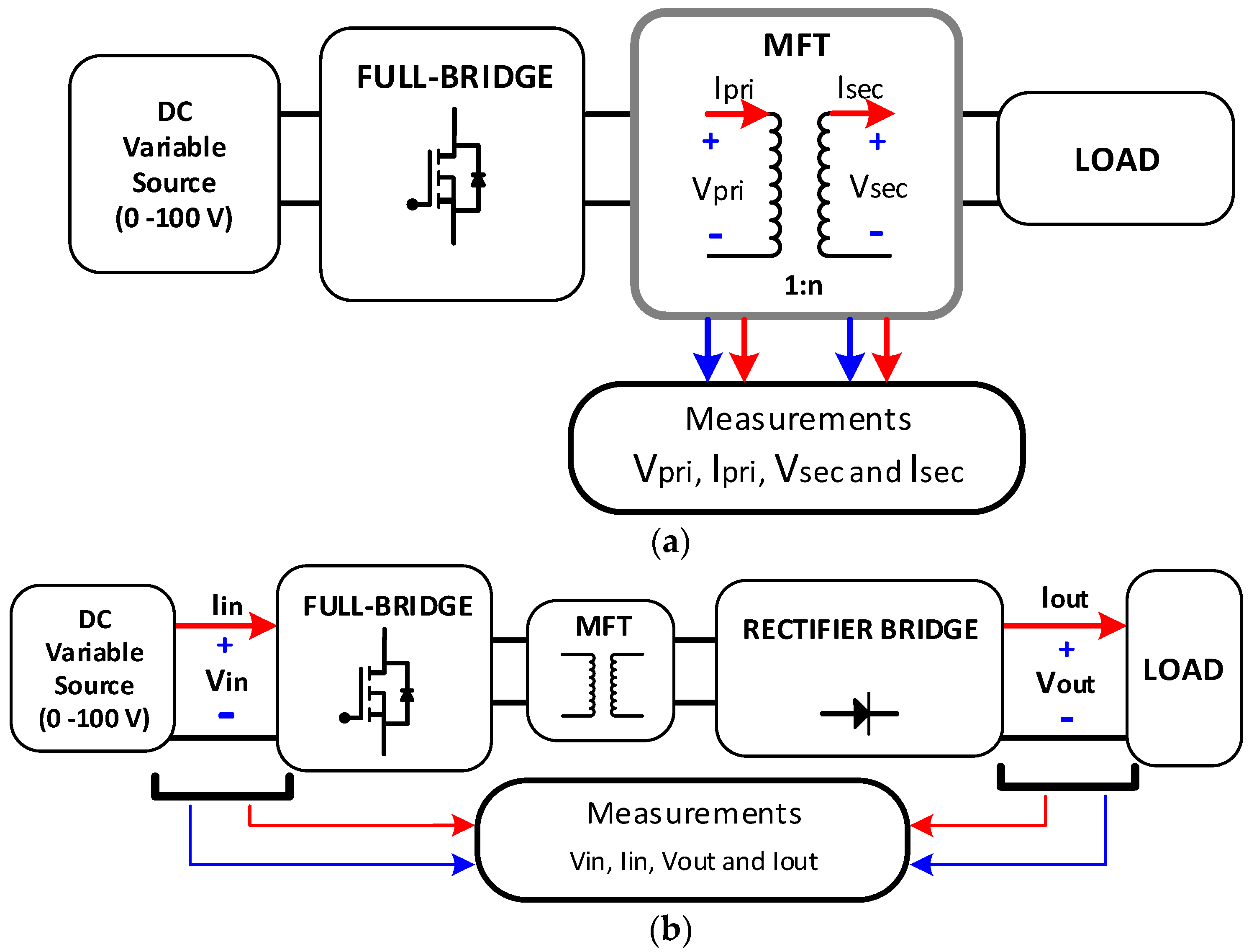
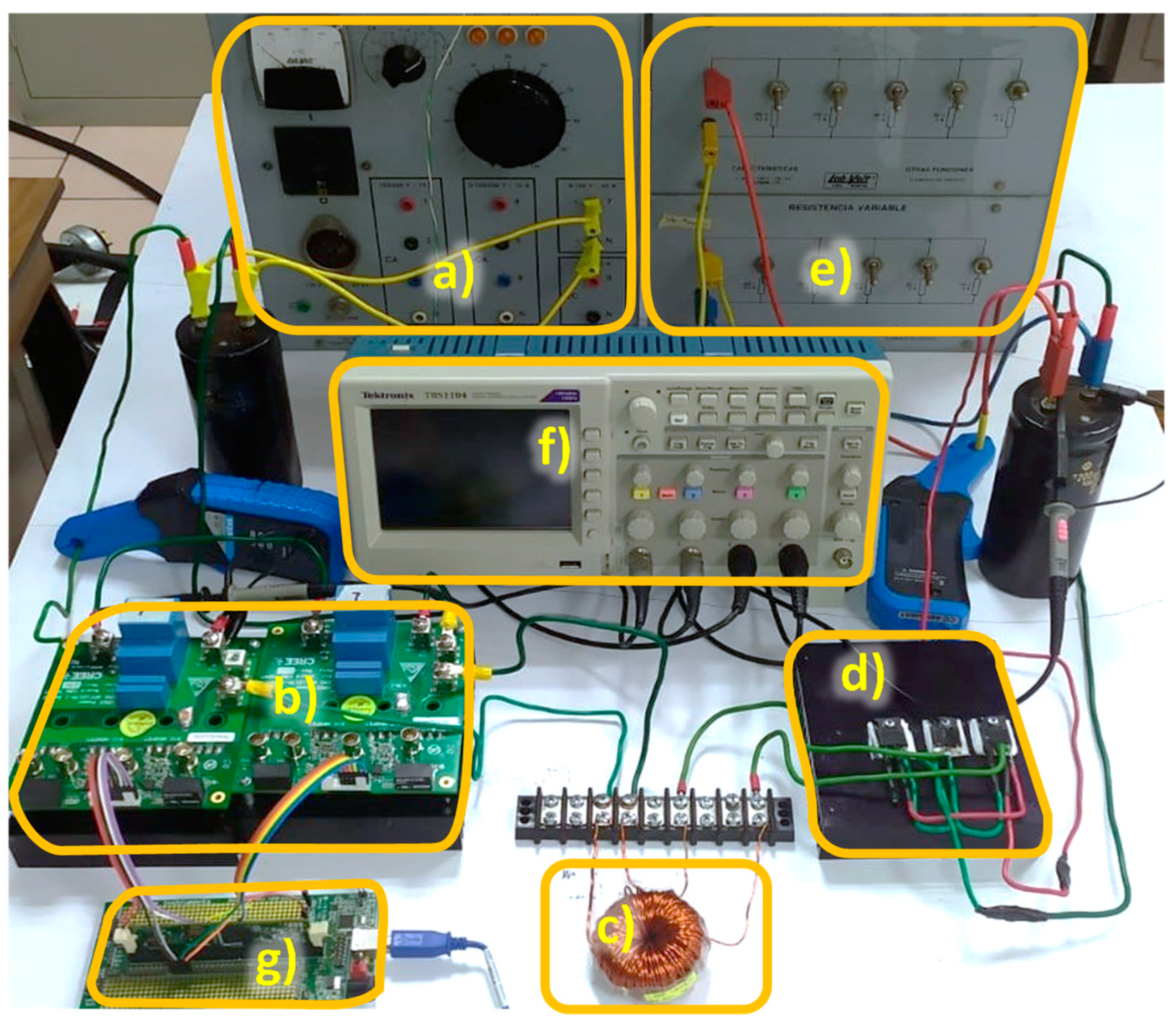
3. FBDC Converter, Simulation, and Experimentation Results

The performance analysis of the multilevel feed transformer was carried out with the linear model, mainly because the design is limited to the linear range of the B (flux density) vs. H (field strength) curve. The model T of the equipment shown in Figure 3 consists of the primary winding, the magnetization branch, and the secondary winding. The primary winding consists of equivalent resistance and the primary leakage inductance, while the magnetization branch models the effects present in the core. The secondary winding consists of resistance and leakage inductance. The prototype was designed at 20 kHz to increase its power density [16]. Table 1 shows the values of the detailed model.

3.1. MFT Analysis under Power Supply with Different THD

The linear model of the transformer was first validated with 2L and 3L power supply and later within the FBDC topology. The test topologies are shown in Figure 5 and were implemented in MATLAB-Simulink. The MFT performance and efficiency were determined in Figure 5a topology. The transformer is subjected to 2L and 3L fed, showing the power is the same for both operating conditions. The voltage THD for 2L presents a value of 48.4%, and the current takes 38%.
On the other hand, for 3L, the voltage THD shows 29% and the current 19.6%. Thus, the effect of the modulation on the THD is evident, depicting variations of 19% in voltage and current. The efficiency of the transformer is 99.5% for both cases, validating the high efficiency of operating with different THD in the power supply. The efficiency calculation is presented in Table 2 and considers Equation (9). Figure 6 shows the waveforms for the 2L and 3L tests.
The following test verified the MFT in the FBDC topology. An essential characteristic of this converter is feeding the MFT with different THD while using the same number of semiconductors. The analysis measurements were Vin, Vout, Iin, and Iout, as shown in Figure 5b. The full load measurements of the converter are shown in Figure 7, and the efficiency is calculated by applying Equation (22). Table 2 shows the converter and MFT’s input and output measurements from the simulation as well as the efficiency of both.
Unlike in other publications, the transformation ratio and efficiency of the proposed multilevel topology are not significantly affected when it is fed with different THD, thus validating the reliability of the proposed model [22,23]. Moreover, the FBDC performance is verified from 25% to 100% of the voltage power supply. Figure 8 presents the graph that defines the efficiency behavior of the FBDC converter operating with 2L and 3L power supply. The efficiency variations are 0.6% considering 2L and 3L for 100% of the supply voltage, 0.8% for 75%, 0.9% for 50%, and 1.4% for 25%. In addition, it is shown that from 50% power supply, the converter reaches values of 95% efficiency for both conditions.
Figure 9 shows the losses in each stage of the FBDC converter calculated by applying Equations (7), (14) and (18). The losses present in the MFT have the same behavior and a similar value with different THD levels confirming the model’s performance. On the other hand, the highest concentration of losses is found in the rectification stage and operating with 2L. This is mainly due to the difference in duty cycle between the 3L, which represents a value of δ = 0.36 and 2L, where δ = 0.5 Thus when applying Equations (18)–(20), in 2L, the value of losses is higher.

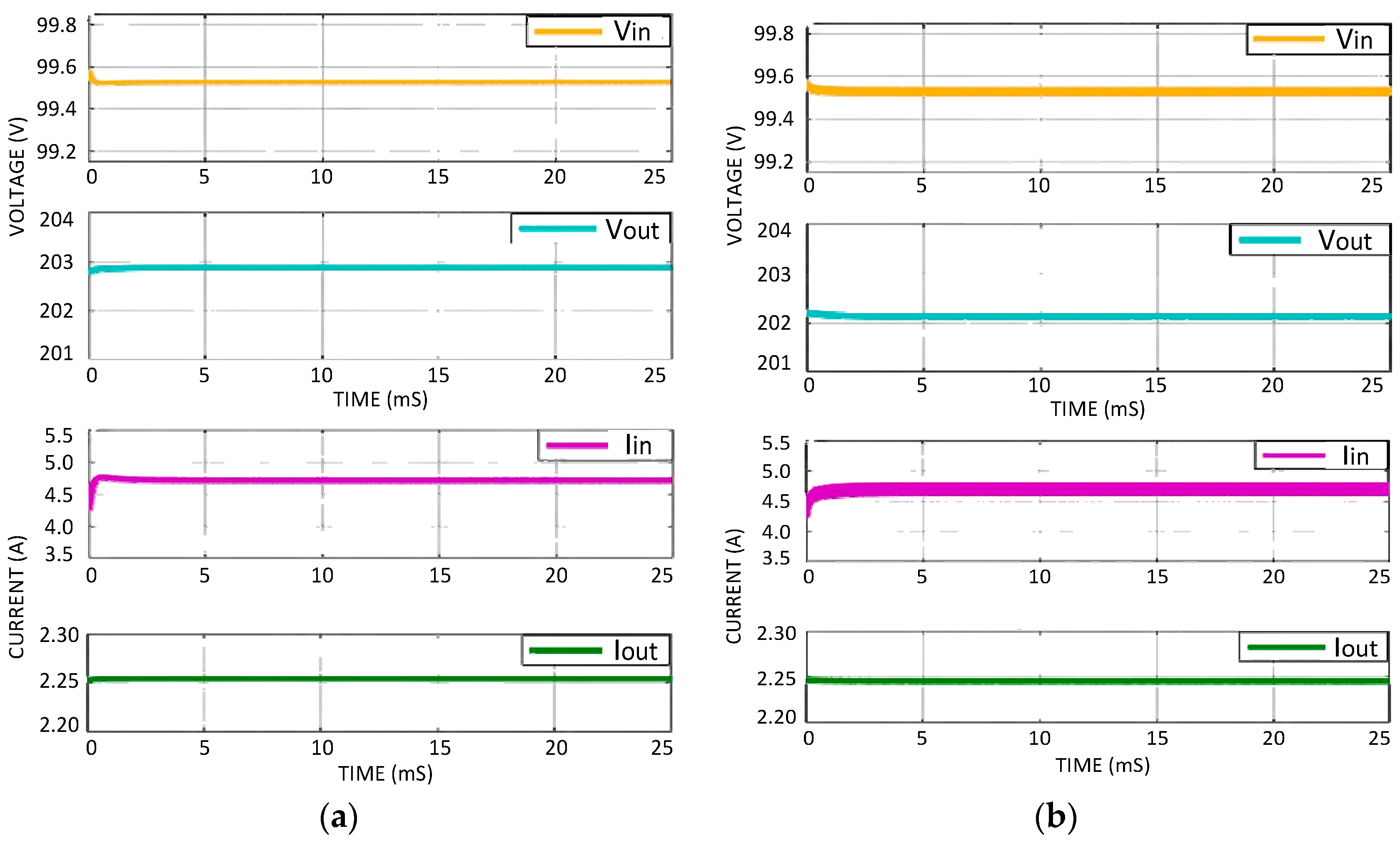
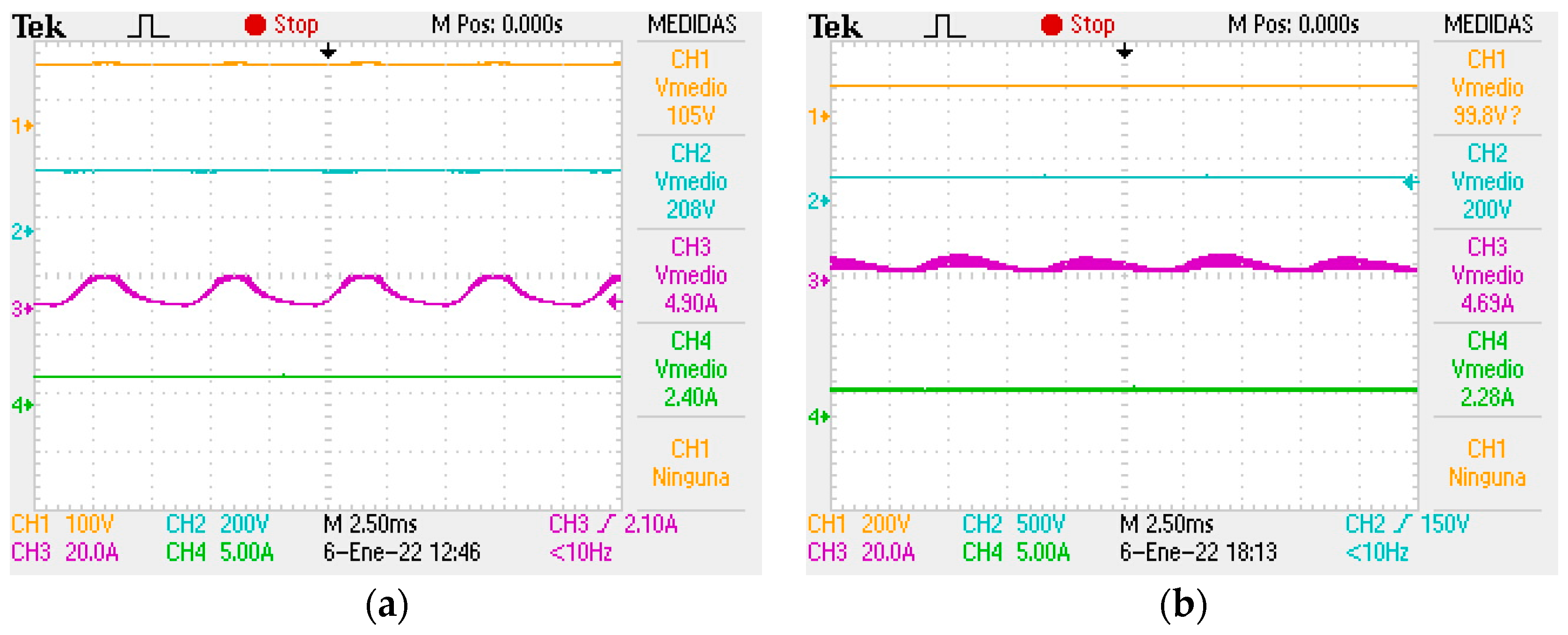
3.2. Experimental Results
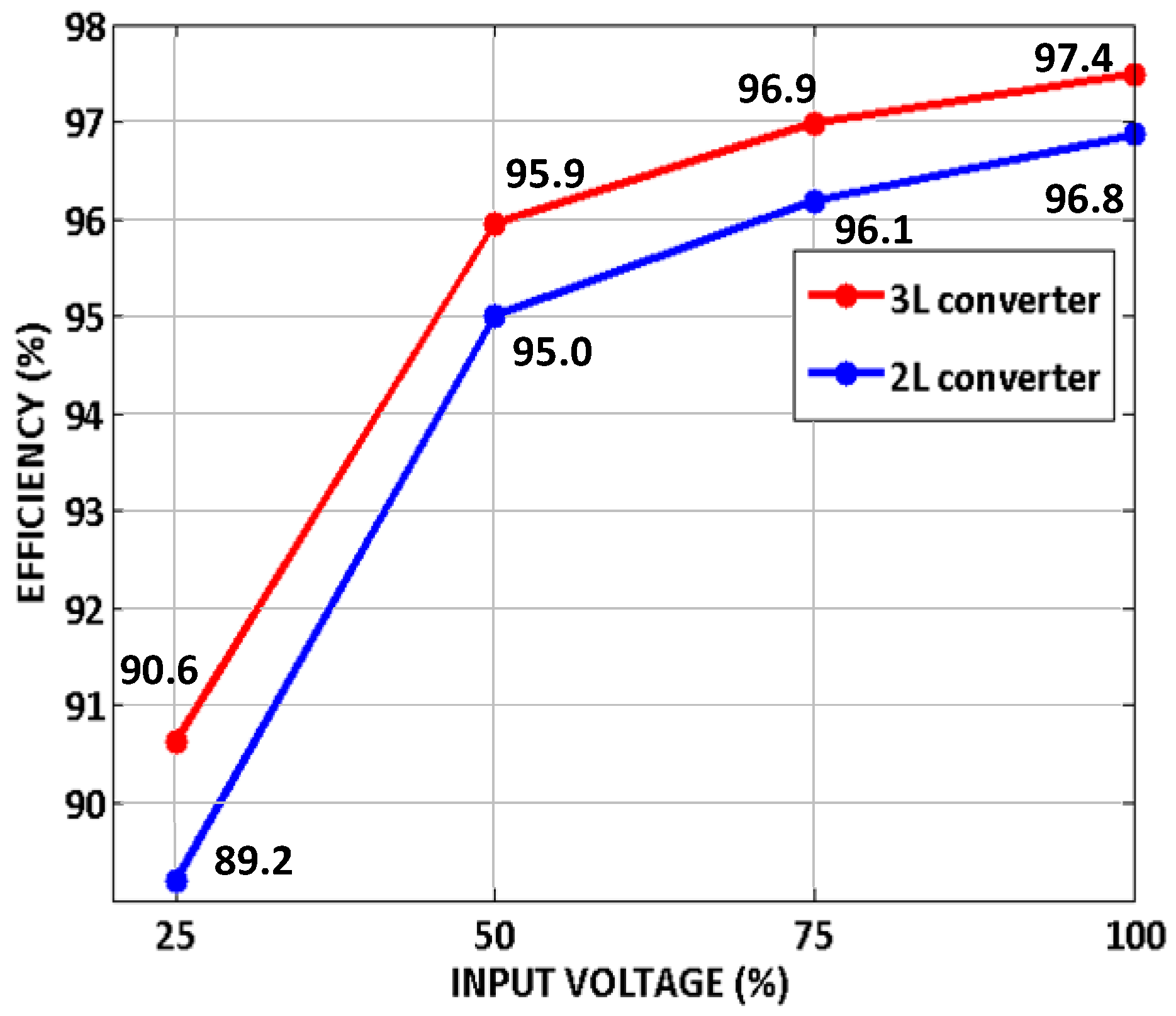
The design methodology described in Chapter 2 was validated in the laboratory. The resulting 100–200 V, 500 VA, and 20 kHz prototypes consider a nanocrystalline toroidal core and solid copper conductor for both windings. The design results are presented in Table 3.
The active implemented stage consists of four silicon carbide power MOSFETs (C2M0025120D); the prototype described in Table 3 corresponds to the isolation stage, and the rectification stage consists of four power diodes (C4D20120D). The measuring equipment is a Tektronix-TBS1104 oscilloscope, voltage probes with ×100 attenuation, and current clamps. AC current measurements use Fluke 80 i 1000 s clamps, and Hantek-CC-65 clamps are used for DC measurements. The modulation signals are generated with a DSP PICCOLO-S28335.
The prototype tests follow the sequence of the simulation. Therefore, the first assembled circuit corresponds to Figure 5a, and MFT efficiency operating with 2L and 3L power supply are determined. In Figure 10, the AC measurements of the MFT prototype are shown.
The prototype efficiency is determined by applying Equation (9) and the oscilloscope measurements; for 2L, it reaches 99.55%, and for 3L, it reflects a value of 99.57%. The results show the high efficiency and performance of the transformer and confirm that the design is adequate since the efficiency remains at a high value for 2L and 3L power supply.
The second test corresponds to the FBDC, the diagram is shown in Figure 5b, and the prototype is in Figure 11. The test determines the efficiency of the converter and the performance of the transformer under 2L and 3L power supply within a DC-DC topology. The test corresponds to nominal power and sufficient time to be considered a steady state. In Figure 12, the DC signals at the ends of the FBDC topology are shown.
The losses in the transformer, active, and passive elements are determined from the measurements. The converter efficiency is calculated using Equation (22), and the results are 97.3% for 3L and 96.7% for 2L. The FBDC efficiency validates the correct operation and performance of the transformer with 2L and 3L power supplies. The MFT is verified under resistive conditions and within a DC-DC topology. Additionally, a sweep is performed on the supply voltage of the FBDC topology from 25% to 100%. This test aims to determine the reliability of the MFT under different operating conditions. Figure 13 shows the efficiency curves of the FBDC with variations in its power supply.
Figure 14 shows the losses in each prototype stage at different power levels. As in the simulation, it is found that a concentration of losses in the diodes reaches the highest values with a power supply of 2L, and it is due to the duty cycle. The prototype tests confirm the behavior presented in the simulation, so the transformer model is validated. In addition, these results indicate that the converter operating with 3L reaches a higher efficiency. Finally, the reliability of the transformer is verified since the efficiency of the FBDC multilevel topology, with 2L and 3L power supply, reflects variations of no more than 1% for the entire voltage range.

4. Discussion

Table 4 compares multilevel topologies where power, frequency, efficiency, and the number of semiconductor devices are considered. It is found that the efficiency of the MFT is 99.7%; for the FBDC converter, it is 97% at full load. Both values are reached with three-level signals.
A crucial stage in isolated converters is the design of the transformer. The design and construction steps of the transformer are proposed, and their respective efficiencies are presented. In Table 4, lower efficiencies for the MFT are presented in [5,19,22] compared to the current investigation. This difference is mainly attributed to the core material, geometry, and design methodology. In [4,5,23,27], the actual behavior of the transformer needs to be considered since it is considered ideal. On the other hand, in [6,19,22], the characteristics and considerations for each prototype are mentioned.
The modulation strategies are of significant impact, the authors in [4,5,6,19,23] propose their modulation strategy, and there is a switching without losses. The control implemented in this research is an open loop for both 2L and 3L. This control allows for the generation with the same topology and different power conditions of the MFT. The main difference is found in the integration of a phase.
Frequently, the calculation of losses in semiconductors and transformers needs to be more detailed. In [6], this estimate is considered; however, a detailed calculation needs to be presented for diodes. In this investigation, a detailed loss estimate is considered for each stage. The MFT losses are determined from design, and the semiconductor elements are calculated from the operating conditions, as stated in [33,34,35].
It is mentioned in [22,23] that the reduction in the THD positively influences the converter’s efficiency. For the multilevel DC-DC topology implemented in this research, this positive effect on efficiency is confirmed when the number of converter levels increases.
However, for [22], when varying the THD, the gain in efficiency in the converter is 11%. In this investigation, the maximum gain in efficiency is 1.9% at 25% of its power supply; at full load, this margin decreases to a difference of 0.4%.
In this way, the positive effect of considering power supply with different THD from the design stage of the MFT is ratified, leading to higher efficiencies. These results open the possibility of new studies by integrating the MFT presented in this research in multilevel topologies such as those mentioned in Table 4.

5. Conclusions

In this research, a DC-DC converter that considers different THD conditions in its power supply was presented and validated. In the operation of multilevel topologies, the model and efficiency of the central stage, which is the transformer, should be more frequently addressed. In this investigation, a detailed methodology was presented in which the necessary characteristics and design considerations are determined so that the prototype reaches high efficiency and reliability in its operation. An MFT prototype was designed and built, considering 2L and 3L power, operating at 20 kHz, 1 to 2 ratio, and 500 W power. The resulting model of the prototype is simulated in MATLAB-Simulink, and verified in the prototype, operating within the FBDC. At full load, the MFT efficiency obtained is 99% and 97% for the FBDC in both conditions, respectively.
In this way, the high performance and effectiveness of the transformer design methodology are validated, operating in multilevel topologies, and high efficiency is obtained in the proposed DC-DC converter (FBDC). This type of converter is essential in applications such as photovoltaic systems, wind systems, electric vehicles, solid-state transformers, and smart grids, where the efficient use of energy is a crucial point for different applications. In addition, this research contributes to increasing the interest in clean energy, and with the above, obtaining a more significant impact in reducing carbon dioxide emissions, reducing the use of non-renewable energy sources, and positively impacting climate change, which is currently a topic of great interest.

Author Contributions

Conceptualization, J.O.-M. and D.G.-R.; methodology, J.O.-M.; software, D.G.-R.; validation, J.O.-M., D.R.-R. and D.G.-R.; formal analysis, D.R.-R.; investigation, J.O.-M.; resources, V.V.-R.; data curation, V.V.-R.; writing—original draft preparation, J.O.-M.; writing—review and editing, D.R.-R.; visualization, D.G.-R.; supervision, D.R.-R.; project administration, V.V.-R.; funding acquisition, V.V.-R. All authors have read and agreed to the published version of the manuscript.

Funding

This research received no external funding.

Data Availability Statement

Acknowledgments

This work was supported by UNAM-PAPIIT <IA104923>. The authors thanks to CONACYT for supporting our research and projects leading to the writing of the present paper.

Conflicts of Interest

The authors declare no conflict of interest.

References

  1. Luo, J.; Bu, S.; Chung, C. Design and comparison of auxiliary resonance controllers for mitigating modal resonance of power systems integrated with wind generation. IEEE Trans. Power Syst. 2021, 36, 3372–3383. [Google Scholar] [CrossRef]
  2. Raghavendra, K.V.G.; Zeb, K.; Muthusamy, A.; Krishna, T.N.V.; Prabhudeva Kumar, S.V.S.V.; Kim, D.-H.; Kim, M.-S.; Cho, H.-G.; Kim, H.-J. A comprehensive review of DC–DC converter topologies and modulation strategies with recent advances in solar photovoltaic systems. Electronics 2020, 9, 31. [Google Scholar] [CrossRef] [Green Version]
  3. Sai, T.; Moon, Y.; Sugimoto, Y. Improved Quasi-Z-Source High Step-Up DC–DC Converter Based on Voltage-Doubler Topology. Sensors 2022, 22, 9893. [Google Scholar] [CrossRef] [PubMed]
  4. Kim, D.; Kim, M.-S.; Nengroo, S.H.; Kim, C.-H.; Kim, H.-J. LLC resonant converter for LEV (Light Electric Vehicle) fast chargers. Electronics 2019, 8, 362. [Google Scholar] [CrossRef] [Green Version]
  5. Hong, T.; Zhi, G.; Qi, K.; Zhao, X.; Ambrosio, J.; Gu, D. A Wide Range Unidirectional Isolated DC-DC Converter for Fuel Cell Electric Vehicles. IEEE Trans. Ind. Electron. 2021, 68, 5932–5943. [Google Scholar] [CrossRef]
  6. Srivastava, M.; Kumar, A.; Singh, P. Design and analysis of customised pulse width modulation based dc–dc converter for EV battery charging application. IET Power Electron. 2020, 13, 3549–3559. [Google Scholar] [CrossRef]
  7. Zhao, L.; Luo, Z.; Fan, Z.; Shi, Y. A dual half-bridge converter with hybrid rectifier for DC power supply in railway systems. IEEE Trans. Power Electron. 2019, 35, 4579–4587. [Google Scholar] [CrossRef]
  8. Marzang, V.; Hashemzadeh, S.; Alavi, P.; Khoshkbar-Sadigh, A.; Hosseini, S.; Malik, M.Z. A Modified Triple-Switch Triple-Mode High Step-Up DC–DC Converter. IEEE Trans. Ind. Electron. 2022, 69, 8015–8027. [Google Scholar] [CrossRef]
  9. Alhurayyis, I.; Elkhateb, A.; Morrow, J. Isolated and nonisolated DC-to-DC converters for medium-voltage DC networks: A review. IEEE J. Emerg. Sel. Top. Power Electron. 2020, 9, 7486–7500. [Google Scholar] [CrossRef]
  10. Mumtaz, F.; Yahaya, N.Z.; Meraj, S.T.; Singh, B.; Kannan, R.; Ibrahim, O. Review on non-isolated DC-DC converters and their control techniques for renewable energy applications. Ain Shams Eng. J. 2021, 12, 3747–3763. [Google Scholar] [CrossRef]
  11. Hashemzadeh, S.M.; Marzang, V.; Pourjafar, S.; Hosseini, S.H. An Ultra High Step-Up Dual-Input Single-Output DC–DC Converter Based on Coupled Inductor. IEEE Trans. Ind. Electron. 2022, 69, 11023–11034. [Google Scholar] [CrossRef]
  12. Ram, B.; Paul, A.; Kulkarni, S. Soft magnetic materials and their applications in transformers. Magnet. and Mag. Mat. 2021, 537, 168210. [Google Scholar] [CrossRef]
  13. Chen, H.; Divan, D. High-frequency transformer design for the soft-switching solid state transformer (S4T). In Proceedings of the 2017 IEEE Applied Power Electronics Conference and Exposition (APEC), Tampa, FL, USA, 26–30 March 2017; pp. 2534–2541. [Google Scholar] [CrossRef]
  14. Huang, P.; Mao, C.; Wang, D.; Wang, L.; Duan, Y.; Qiu, J.; Xu, G.; Cai, H. Optimal design and implementation of high-voltage high-power silicon steel core medium-frequency transformer. IEEE Trans. Ind. Electron. 2017, 64, 4391–4401. [Google Scholar] [CrossRef]
  15. Ruiz, D.; Venegas-Rebollar, V.; Anaya-Ruiz, A.; Moreno-Goytia, E.L.; Rodríguez-Rodríguez, J.R. Design and prototyping medium-frequency transformers featuring a nanocrystalline core for dc–dc converters. Energies 2018, 11, 2081. [Google Scholar] [CrossRef] [Green Version]
  16. Ruiz, D.; Ortíz, J.; Moreno, E.; Fuerte, C.; Venegas, V.; Vargas, A.; Vergara, H. Ferrites and Nanocrystalline Alloys Applied to DC–DC Converters for Renewable Energies. Appl. Sci. 2022, 12, 709. [Google Scholar] [CrossRef]
  17. Rodriguez, J.; Sheng, J.; Zheng, F. Multilevel inverters: A survey of topologies, controls, and applications. IEEE Trans. Ind. Electron. 2002, 49, 724–738. [Google Scholar] [CrossRef] [Green Version]
  18. Yan, Y.; Huang, Y.; Chen, R.; Bai, H. Building Common-Mode Analytical Model for Dual Active Bridge Incorporating with Different Modulation Strategies. IEEE Trans. Power Electron. 2021, 36, 12608–12619. [Google Scholar] [CrossRef]
  19. Moonem, M.; Pechacek, C.; Hernandez, R.; Krishnaswami, H. Analysis of a multilevel dual active bridge (ML-DAB) DC-DC converter using symmetric modulation. Electronics 2015, 4, 239–260. [Google Scholar] [CrossRef] [Green Version]
  20. Lin, B. DC–DC converter implementation with wide output voltage operation. J. Power Electron. 2020, 20, 376–387. [Google Scholar] [CrossRef]
  21. Han, J.; Moon, G. High-efficiency phase-shifted full-bridge converter with a new coupled inductor rectifier (CIR). IEEE Trans. Power Electron. 2019, 34, 8468–8480. [Google Scholar] [CrossRef]
  22. Ozdemir, S.; Balci, S.; Altin, N.; Sefa, I. Design and performance analysis of the three-level isolated DC-DC converter with the nanocyrstalline core transformer. Int. J. Hydrog. Energy 2017, 42, 17801–17812. [Google Scholar] [CrossRef]
  23. Liu, D.; Wang, Y.; Deng, F.; Chen, Z. Triple-phase-shift modulation strategy for diode-clamped full-bridge three-level isolated DC/DC converter. IEEE Access 2019, 8, 2750–2759. [Google Scholar] [CrossRef]
  24. Liu, D.; Wang, Y.; Zhang, Q.; Chen, Z. ZVZCS full-bridge three-level DC/DC converter with reduced device count. IEEE Trans. Power Electron. 2020, 35, 9965–9970. [Google Scholar] [CrossRef]
  25. Zhao, L.; Chen, J.; Chen, T.; Shi, Y.; Fan, Z.; Zhuang, Z. Zero-voltage and zero-current switching dual-transformer-based full-bridge converter with current doubler rectifier. IEEE Trans. Power Electron. 2020, 35, 12949–12958. [Google Scholar] [CrossRef]
  26. Liu, D.; Deng, F.; Zhang, Q.; Chen, Z. Periodically swapping modulation (PSM) strategy for three-level (TL) DC/DC converters with balanced switch currents. IEEE Trans. Ind. Electron. 2017, 65, 412–423. [Google Scholar] [CrossRef] [Green Version]
  27. Shi, Y.; Wang, X.; Xi, J.; Gui, X.; Yang, X. Wide load range ZVZCS three-level DC–DC converter with compact structure. IEEE Trans. Power Electron. 2018, 34, 5032–5037. [Google Scholar] [CrossRef]
  28. Liu, P.; Chen, C.; Duan, S.; Jin, L.; Zhu, W. A three-level rectifier structure with flying capacitors for DC–DC converter in high-voltage output application. IEEE Trans. Ind. Electron. 2017, 65, 2122–2134. [Google Scholar] [CrossRef]
  29. McLyman, C. Power Transformer Design. In Transformer and Inductor Design Handbook; CRC Press: Boca Raton, FL, USA, 2011; ISBN 978-1-4398-3688-0. [Google Scholar]
  30. Hilzinger, R. Magnetic Materials; Germany Publishing: Erlangen, Germany, 2013; ISBN 978-3895783524. [Google Scholar]
  31. Colak, I.; Kabalci, E.; Bayindir, R. Review of multilevel voltage source inverter topologies and control schemes. Energy Convers. Manag. 2011, 52, 1114–1128. [Google Scholar] [CrossRef]
  32. Rana, R.; Patel, S.A.; Muthusamy, A.; Lee, C.W.; Kim, H.-J. Review of multilevel voltage source inverter topologies and analysis of harmonics distortions in FC-MLI. Electronics 2019, 8, 1329. [Google Scholar] [CrossRef] [Green Version]
  33. Revathi, B.; Mahalingam, P.; Gonzalez, F. Interleaved high gain DC-DC converter for integrating solar PV source to DC bus. Sol. Energy 2019, 188, 924–934. [Google Scholar] [CrossRef]
  34. Ahmed, M.; Wang, M.; Shehzad, M.; Ullah, I. Power loss model and efficiency analysis of three-phase inverter based on SiC MOSFETs for PV applications. IEEE Access 2019, 7, 75768–75781. [Google Scholar] [CrossRef]
  35. Hafezi, H.; Faranda, R. A new approach for power losses evaluation of IGBT/diode module. Electronics 2021, 10, 280. [Google Scholar] [CrossRef]
Figure 1. MFT Design methodology.
Electronics 12 01110 g001
Figure 2. Toroidal core geometry.
Electronics 12 01110 g002
Figure 3. FBDC Topology.
Electronics 12 01110 g003
Figure 4. Modulation signals: (a) 2L, (b) 3L.
Electronics 12 01110 g004
Figure 5. Topology: (a) MFT efficiency test and (b) FBDC.
Electronics 12 01110 g005
Figure 6. MFT AC waveforms: (a) 2-Level and (b) 3-Level.
Electronics 12 01110 g006
Figure 7. DC signals are measured in (a) 2-Level and (b) 3-Level converters.
Electronics 12 01110 g007
Figure 8. Converter efficiency from simulation measurements.
Electronics 12 01110 g008
Figure 9. Loss percentages in (a) 2L and (b) 3L converters.
Electronics 12 01110 g009
Figure 10. AC signals in the MFT: (a) 2L and (b) 3L.
Electronics 12 01110 g010
Figure 11. Laboratory prototype of FBDC topology: (a) DC variable source 0–120 V, (b) Full-bridge, (c) MFT, (d) Rectifier bridge, (e) Load, (f) Oscilloscope, and (g) DSP.
Electronics 12 01110 g011
Figure 12. DC voltage and current signals from converter at full load: (a) 2L and (b) 3L.
Electronics 12 01110 g012
Figure 13. Efficiencies for 2L and 3L converters.
Electronics 12 01110 g013
Figure 14. Percentage of losses in the converter of (a) 2L and (b) 3L.
Electronics 12 01110 g014
Table 1. MFT’s Parameters.
VariableValue
Pnom500 VA
V1100 V
V2200 V
f20 kHz
R116.5 mΩ
R268.5 mΩ
Ld10.5 µH
Ld22.1 µH
Rm8832 Ω
Lm35.4 mH
Table 2. Input and output voltages and currents for efficiency simulation in the converter and MFT.
LevelsVpri
Vin
Vsec
Vout
Ipri
Iin
Isec
Iout
Efficiency
MFT2L99.3 V197.8 V
200.3 V
4.41 A
4.46 A
2.2 A
2.23 A
99.54%
99.55%
3L100.5 V
DC-DC Converter2L99.5 V
99.5 V
202.9 V
202.2 V
4.75 A
4.71 A
2.25 A
2.25 A
96.8%
97.4%
3L
Table 3. MFT’s parameters.
ParameterValue
Core materialNanocrystalline
(Vitroperm 500F, W514)
Frequency20 kHz
Core typeToroidal
Core dimensions3 × 2 × 1.5 cm
Np20 turns
Ns41 turns
Primary winding calibre15 AWG
Secondary winding calibre18 AWG
Flux density0.8 T
Permeability53, 355
Table 4. Isolated DC-DC converters with high efficiency.
Ref.Freq.
(kHz)
Power
(W)
No. DevicesConverter Efficciency
(%)
TransformerYear
Semi-
Conductor
PassiveDesignMaterialEfficiency
(%)
[4]30–10010008496.4/96.2/96.42019
[5]10025008594.5Ferrites 98.2 2021
[6]805408391.4Ferrites2020
[19]5334016488.0Amorphous 93.02015
[22]1050008/162/481.0/92.0Nanocryst.94.0/96.02017
[23]50100016793.32019
[27]100110010695.02018
This proposal205008296.6/97.0Nanocryst.99.6/99.7
Disclaimer/Publisher’s Note: The statements, opinions and data contained in all publications are solely those of the individual author(s) and contributor(s) and not of MDPI and/or the editor(s). MDPI and/or the editor(s) disclaim responsibility for any injury to people or property resulting from any ideas, methods, instructions or products referred to in the content.

