Article

Characterization of Sn-xIn Solders and Thermomigration-Induced Interfacial IMC Growth of Cu/Sn-xIn/Cu Micro Solder Joints

School of Materials Science and Engineering, Dalian University of Technology, Dalian 116024, China
*
Author to whom correspondence should be addressed.
Electronics 2023, 12(8), 1899; https://doi.org/10.3390/electronics12081899
Submission received: 8 March 2023 / Revised: 4 April 2023 / Accepted: 14 April 2023 / Published: 18 April 2023
(This article belongs to the Special Issue Advanced Electronic Packaging Technology)

Abstract

:
The melting behavior and microstructure of bulk Sn-xIn (x = 6, 12 and 24, wt.%) solders and the thermomigration, elemental distribution and intermetallic compound (IMC) growth in Cu/Sn-xIn/Cu micro solder joints during soldering and aging under temperature gradient (TG) were investigated. The results indicate that In addition effectively decreased the melting temperature of the bulk solders. Only the InSn4 phase was detected when In addition was increased to 24 wt.%. During soldering under TG, the growth rate of the interfacial IMC layer at the cold end interfaces gradually decreased as the In content increased. The mechanism of microstructure evolution and elemental distribution in the micro solder joints was revealed based on the TG-induced atomic thermomigration (TM). The chemical potential gradient of atoms was enhanced by TM, and the rapid diffusion of atoms in the liquids resulted in a uniform distribution of In element in both solders and the IMC phase during soldering. While during aging under TG, there was a smaller chemical potential gradient due to the slow atomic diffusion rate. At this time, TG dominated the atomic migration, which resulted in a nonuniform distribution of the In element in the whole joints. This study provides further insight into the application of In-containing solders in electronic packaging.

1. Introduction

In electronic packaging technology, solder alloys are used as filler material to assemble and interconnect various components. Sn-Pb solders were widely used in early industry, but many countries have legally restricted the use of Pb in solders due to its toxicity and pollution problem. Therefore, Sn-based lead-free solders have been developed and applied rapidly in this context, such as Sn-Ag, Sn-Cu, Sn-Zn, Sn-Bi, Sn-In and Sn-Ag-Cu [1,2,3]. Indium (In) is also used in lead-free solders due to its low melting point, good oxidation resistance and fatigue resistance. On the one hand, eutectic In-48Sn solder with a low melting point of 118 °C is used in the processes requiring low-temperature soldering, such as step welding and heat-sensitive devices [4,5]. On the other hand, In is doped as an additional element in solders to optimize microstructure, lower melting temperature and improve mechanical properties [6,7].
In recent years, the microstructure evolution and properties of In-containing solders soldering on various substrates have been widely reported. Copper (Cu) is the most commonly used substrate material in electronic packaging. For eutectic In-48Sn solder, both In and Sn can react with Cu to form several types of interfacial intermetallic compounds (IMCs). Tian et al. found that a Cu(In,Sn)2 layer adjacent to solder and a Cu2(In,Sn) layer adjacent to Cu substrate was formed at the In-48Sn/Cu interface [8]. As an additional element, In can affect not only the microstructure of solders but also the interfacial reaction during soldering. For example, the addition of In to Sn-3.5Ag-0.7Cu, Sn-58Bi and Sn-0.7Cu solders can reduce the melting points of the solders and improve their wettability [9,10,11,12]. Pandey et al. pointed out that the eutectic microstructure became coarser after adding In into Sn-Zn eutectic alloy, and the strength of the solder increased because of the dissolution of In in β-Sn [13]. Moreover, it was reported that the In addition to Sn-Ag solder effectively reduced the formation of large Ag3Sn plates but promoted the formation of irregular polygonal Ag9In4 instead [14]. It was also found that the addition of In could refine the microstructure of solder and improve its strength [15,16]. Moreover, Wang et al. investigated the interfacial reaction between Sn-1.8Ag-9.4In solder and Cu substrate and found that Cu6(Sn,In)5 and Cu3(Sn,In) were formed at the interface after reflow [17]. The addition of In can also affect interfacial IMC growth. Tian et al. reported that In addition had little effect on the growth of Cu6Sn5 during solid-state aging of Sn-0.7Cu-xIn/Cu but strongly inhibited the growth of Cu3Sn [18]. In contrast, Kelly et al. studied the effect of In addition on the electromigration (EM) behavior of Sn-0.7Cu solder joint and found that In addition inhibited the growth of Cu6Sn5 but had no effect on Cu3Sn [19].
Previous studies mainly focused on the properties of Sn-In solders, the interfacial reactions and EM behavior of Sn-In solder joints, while few studies focused on the thermomigration (TM) behavior of In-containing solder joints under temperature gradient (TG). TM is an enhanced directional diffusion process of atoms under TG. Chen et al. studied the microstructure evolution of Cu/Sn-Ag/Cu solder joints under TG and found that the hot-end Cu dissolved severely, and holes formed, while the cold-end interfacial IMC grew aggressively [20], which could significantly affect the reliability of micro solder joints for advanced packaging. In lead-free solder joints, several elements can involve an interfacial reaction and Sn grain orientation also affects the growth of interfacial IMC under TG [21], making TM behavior more complex and diverse. Therefore, knowing atomic TM behavior and its influence on interfacial IMC growth is crucial for the reliability control of solder joints, especially for those in advanced packaging with shrinking size. Furthermore, an in-depth understanding of how In addition affects the IMC formation and microstructure evolution of a solder joint under TG will be critical in In-containing solders for commercial applications.
In this paper, the melting behavior and microstructure of Sn-xIn (x = 6, 12, 24 wt.%) solders were characterized. Then a quasi-in situ observation method was used to investigate the microstructure evolution of Cu/Sn-xIn/Cu solder joints under TG. Finally, the atomic TM behavior and its effect on interfacial IMC growth were discussed.

2. Experimental

The Sn-xIn (x = 6, 12, and 24, wt.%) solders were prepared from pure Sn and In-48Sn. The Sn and In-48Sn were weighed and put into quartz tubes, which were then vacuum encapsulated and heated up to 300 °C. After holding for 2 h, the quartz tubes were taken out and cooled in water. The actual composition of the as-prepared solders was examined to be Sn-6.2In, Sn-12.1In and Sn-23.6In using an X-ray fluorescence spectrometer (XRF-1800, Shimadzu, Japan). The solders were mechanically ground with emery papers, polished by diamond polishing slurry and cleaned with anhydrous ethanol. Then the phase composition and elemental distribution of the solders were examined by using an X-ray diffractometer (XRD-6000, Shimadzu, Japan) and a field emission electron probing microanalysis (EPMA, JXA-8530F PLUS, JEOL, Japan). The melting behavior of the solders was characterized by a differential scanning calorimeter (DSC822) with a heating rate of 10 °C/min and a scanning range of 50–300 °C.
The Cu/Sn-xIn/Cu solder joints were prepared by merging a pair of Cu substrates into the Sn-xIn solders at 250 °C for 15 s. The preparation procedure was similar to the previous study [22]. Afterward, the solder joints were placed on a hot plate for soldering and aging under TG, and the experimental configuration is schematically shown in Figure 1a,b. It should be noted that the interfaces of the joints close to the heat source are named the hot-end interface, while those close to the heat sink are named the cold-end interface. The temperature distribution in the solder layers was simulated by ANSYS software, as shown in Figure 1c,d. The thermal conductivity of Cu used for simulation was 401.0 W/(m2K). The ambient temperature and gravity vector were set to be 20 °C and −9.81 m/s2, respectively. Boussinesq approximation and zero equation of turbulence were used to model the natural convection at the heat preservation stage. The detailed simulation method and process were the same as the previous study [23]. The simulation results indicated that the TG value across the solder layers was all about 600 °C/cm, and the average temperatures of the solder layers were 250 °C for soldering and 150 °C for aging. The durations were 5, 15, 30 and 60 min for soldering and 50, 100, 200 and 400 h for aging. The solder joints were observed by the EPMA in a backscattered electron (BSE) imaging mode, and the thickness of the interfacial IMC was measured using Photoshop based on the EPMA images.

3. Results and Discussion

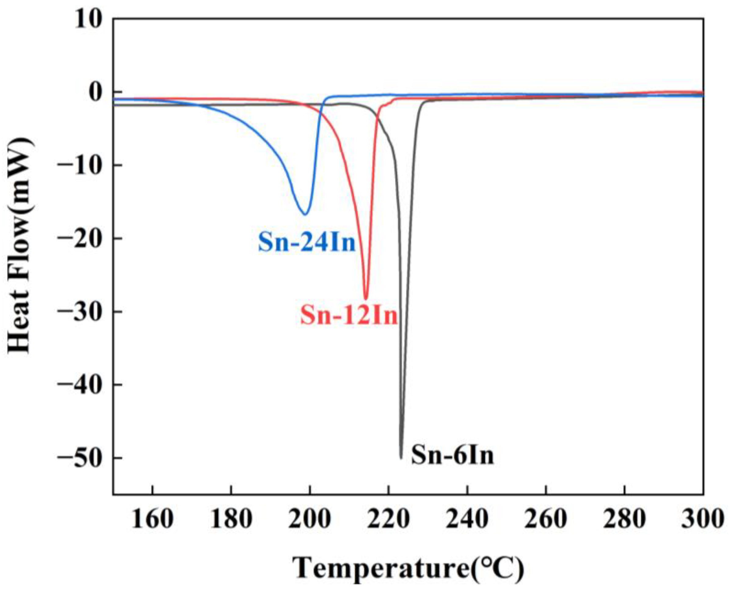
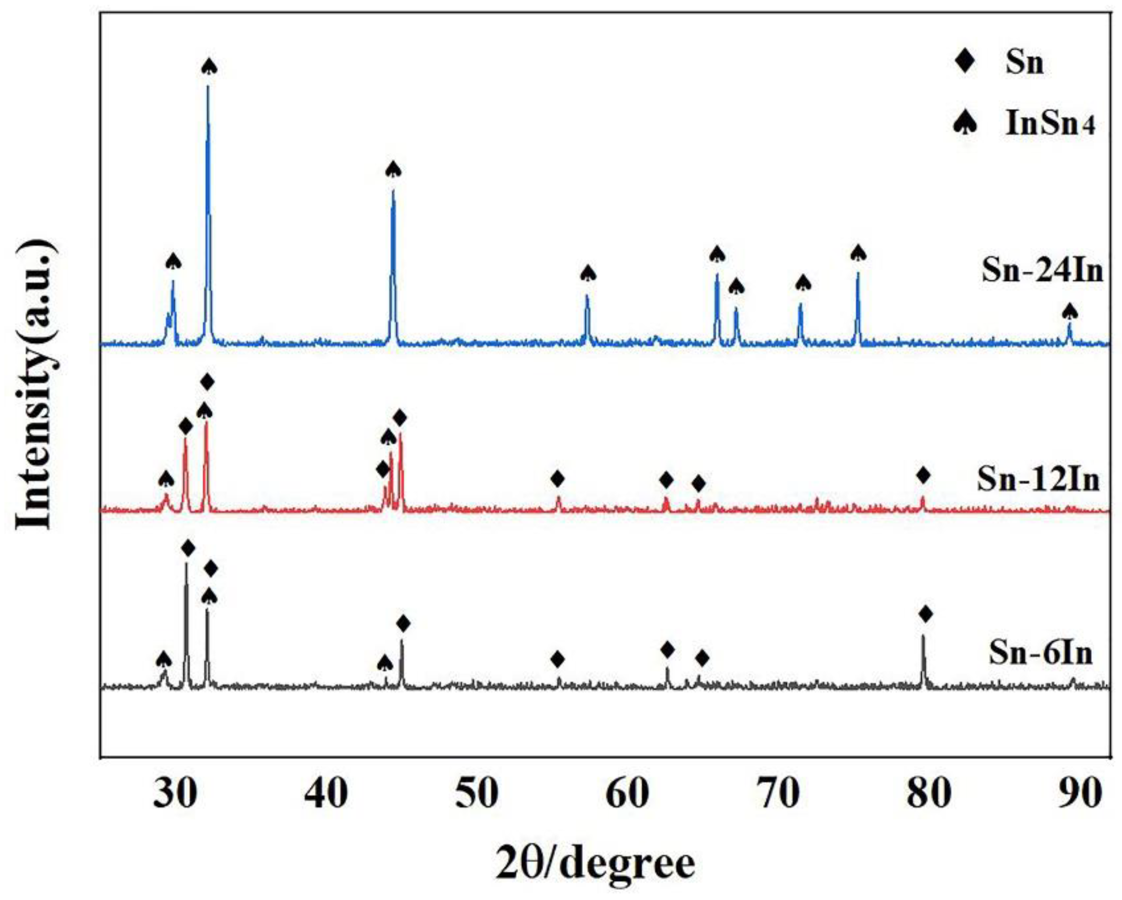
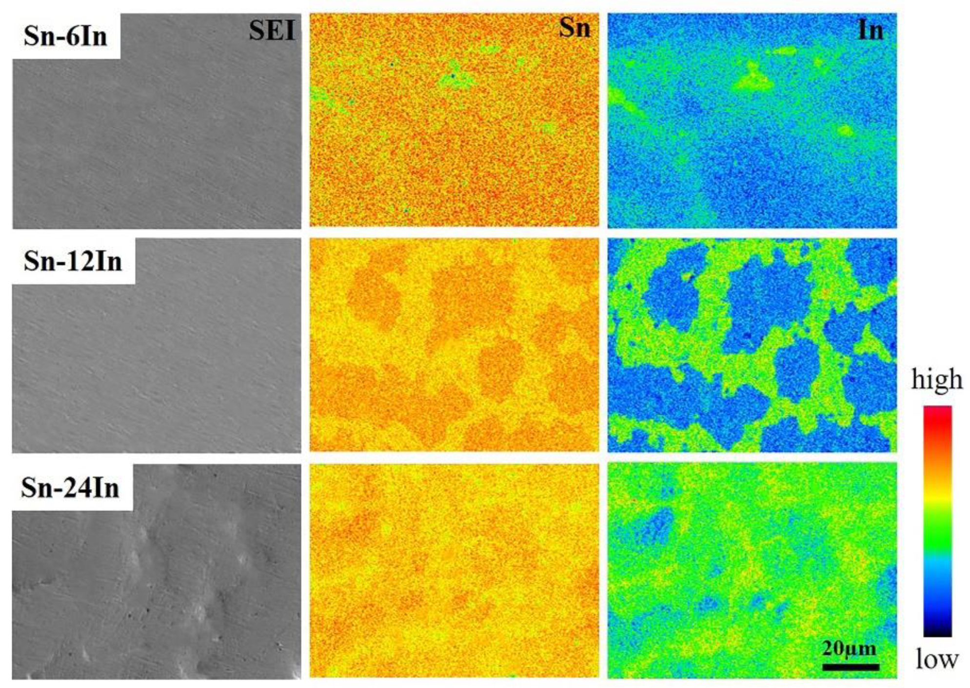
3.1. Characterization of the Sn-xIn Solders

Figure 2 shows the DSC curves of the Sn-xIn solders during heating. There was only one endothermic peak on each DSC curve, and the peak temperature decreased obviously with increasing In content. The melting properties of the Sn-xIn solders were summarized in Table 1. The results showed that the melting points (peak temperatures) of the Sn-xIn solders decreased with increasing In content. The melting point of pure Sn is 232 °C. When 24 wt.% In was added, the melting temperature of the solder decreased to 198.82 °C. Moreover, as the In content increased, the melting range (ΔT) of the solders, which was defined as the temperature difference between the onset of melting temperature (T1) and the offset of melting temperature (T2), also increased. The melting point of solder is a basic parameter for soldering that determines the soldering profile setting. A high-quality solder should have a relatively low melting temperature, and its melting range should be as small as possible. Therefore, comprehensive consideration should be made in practical applications to select an appropriate content of In in solder.
Figure 3 shows the XRD patterns of the Sn-xIn solders. The results indicate that the In addition significantly affected the phase composition of the solders. When a small amount of In was added, the solder contained β-Sn and InSn4. The PDF cards corresponding to the β-Sn phase and InSn4 phase are 04-0673 and 48-1547, respectively. It was reported that the maximum amount of In dissolved in β-Sn was 3.2 wt.%, and InSn4 was generated when In was higher than 3.2 wt.% [15]. With increasing In content, the β-Sn phase in the solder decreased while the InSn4 phase increased. Finally, only the InSn4 phase was detected in the Sn-24In solder without the β-Sn phase, which was consistent with the Sn-In phase diagram. Figure 4 shows the elemental distribution of the Sn-xIn solders. There was a regional aggregation of both Sn and In, and the In-rich region was the InSn4 phase. The elemental distribution results were consistent with the XRD results.

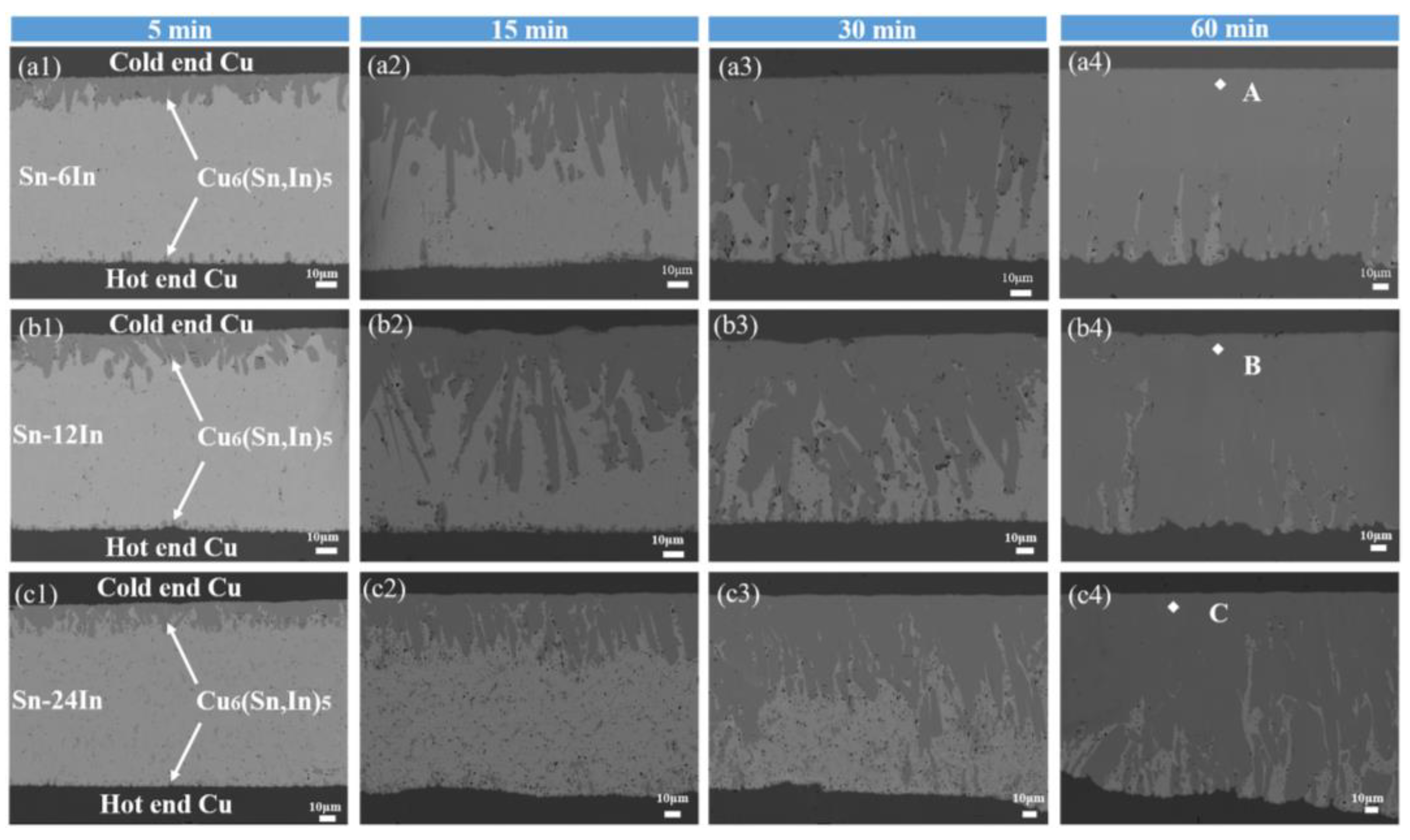
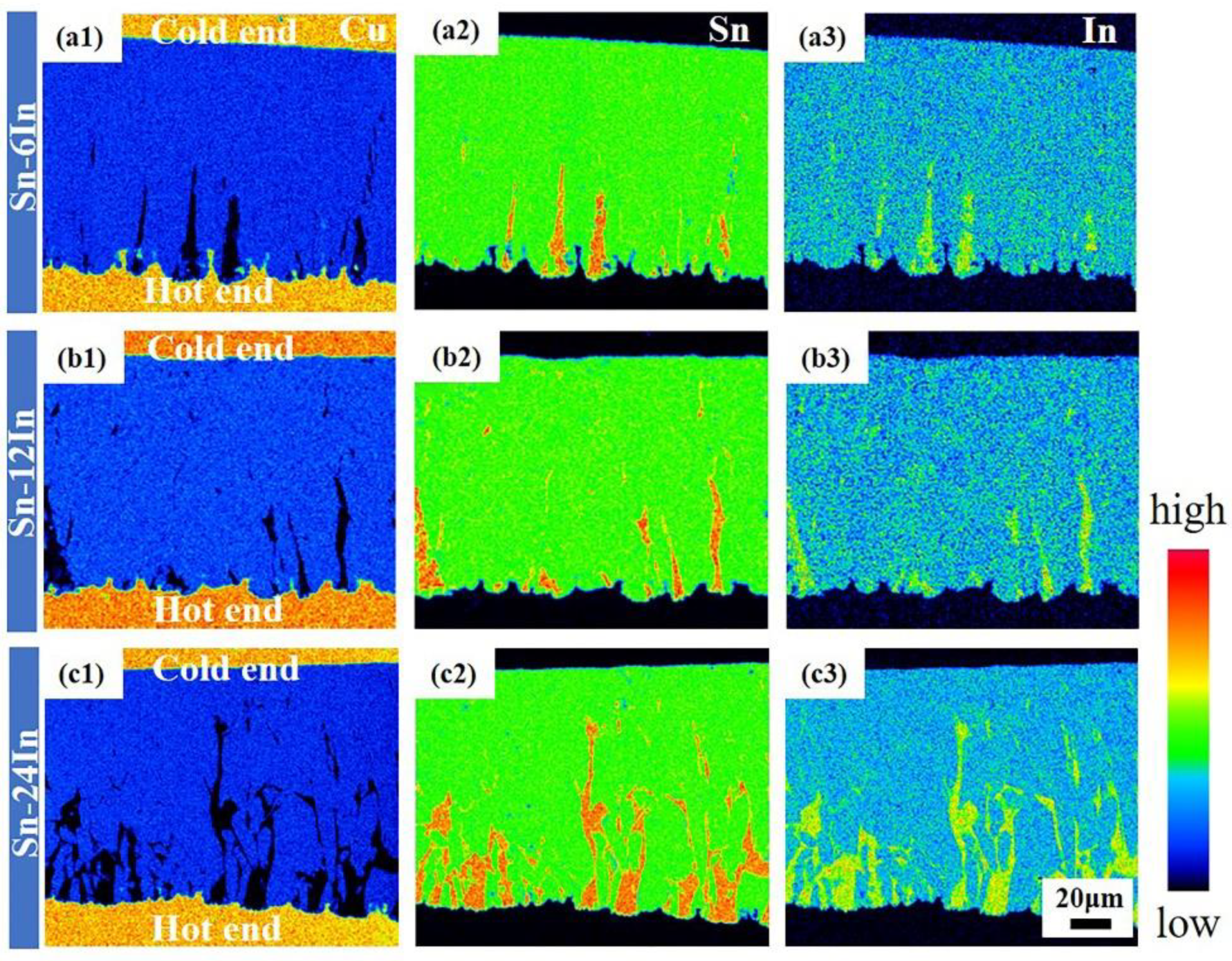
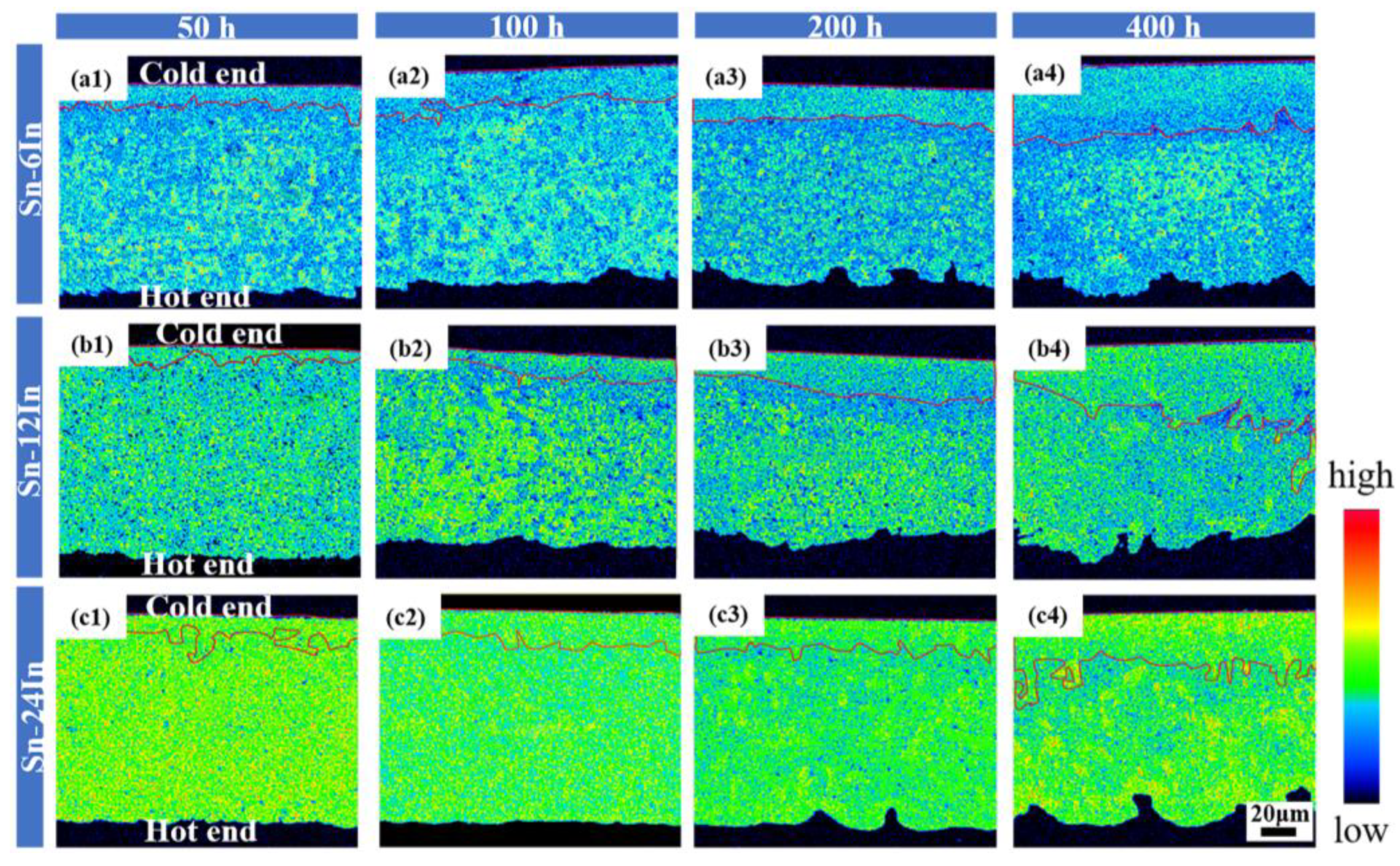
3.2. Microstructure Evolution of the Cu/Sn-xIn/Cu Micro Solder Joints under TG

Figure 5 shows the microstructure evolution of the Cu/Sn-xIn/Cu micro solder joints during soldering under TG for different durations. The interfacial IMC showed asymmetric growth between the cold and hot ends of all the solder joints, with aggressive IMC growth at the cold end and little IMC growth at the hot end. The uneven interface at the hot end indicated severe Cu substrate consumption. Furthermore, the cold-end IMC presented a needle-like morphology and gradually thickened as the soldering time increased. After soldering for 60 min, the cold-end IMC reached the hot-end interfaces for all three cases, indicating that full IMC joints with a small amount of solder residuals were obtained, as shown in Figure 5(a4–c4). Figure 6 shows the elemental distribution of the full IMC joints after soldering under TG for 60 min. The results indicated that Cu, Sn and In were all uniformly distributed in the IMC phase, and no significant element segregation was detected. As for the residual solders, Sn and In were also uniformly distributed.
Figure 7 shows the microstructure evolution of the Cu/Sn-xIn/Cu micro solder joints during aging under TG for different durations. All the micro solder joints showed asymmetric characteristics with aggressive IMC growth at the cold ends and limited IMC growth at the hot ends. The cold-end IMC, which gradually thickened with increasing aging time, presented a laminar morphology. While with increasing In content, the hot-end IMC thickened and blocky IMC was formed in solders. Especially in the Cu/Sn-24In/Cu micro solder joint, the blocky IMC had spread all over the solder after aging under TG for 400 h, as shown in Figure 7(c4). Figure 8 shows the distribution of In in the Cu/Sn-xIn/Cu micro solder joints after aging under TG for different durations. Interestingly, with increasing aging time, significant element segregation was detected in all the micro solder joints. The areas selected by the red solid box in Figure 8 are the cold-end IMC. The distribution of the In element in the cold-end IMC phase was nonuniform, which presented decreasing In content in the newly formed IMC. In addition, in residual solder, there was also an In-poor layer near the cold-end IMC and an In-rich area near the hot end.
Table 2 shows the compositions of the interfacial IMC at the positions A–F marked in Figure 5 and Figure 7. All the IMCs were identified as Cu6(Sn,In)5 based on the atomic ratio, which is consistent with the previous studies [18,24,25]. The radii of Sn and In atoms were 145 pm and 155 pm, respectively [26], and the small difference in the atomic radii between In and Sn could lead to atomic substitution [27]. Some In atoms were substituted for Sn atoms in Cu6Sn5 to form Cu6(Sn,In)5. It could be summarized that the In content of Cu6(Sn,In)5 was basically the same in the Cu/Sn-6In/Cu and Cu/Sn-12In/Cu micro solder joints but was significantly increased in the Cu/Sn-24In/Cu micro solder joint. According to previous studies, the mechanical properties of Cu6(Sn,In)5 seem to be better than those of Cu6Sn5. Huang et al. found that, with In addition, a Sn atom in the structure of Cu6Sn5 was replaced by an In atom to form Cu24Sn19In1. The structural stability of Cu24Sn19In1 was better than that of Cu6Sn5, which was beneficial in improving the mechanical properties of the IMC layer [28].

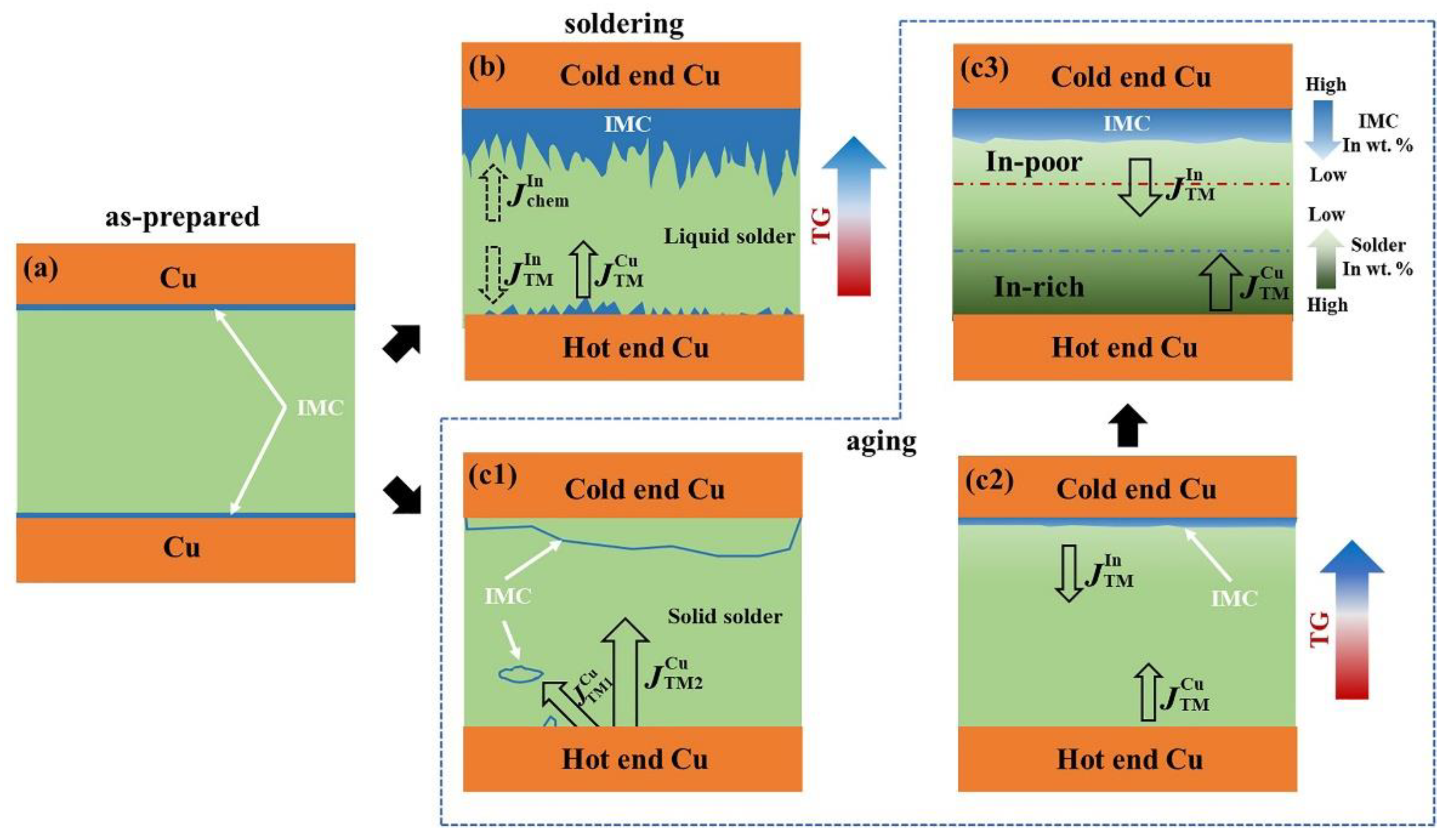
3.3. Mechanism of the Microstructure Evolution in the Micro Solder Joints

The Cu/Sn-xIn/Cu micro solder joints exhibited different microstructure evolution and element distribution during soldering and aging under TG. It was reported that Cu atoms migrated from the hot end to the cold end under TG, resulting in a large thermomigration flux of Cu atoms, a thick IMC layer at the cold end and a serious Cu substrate dissolution and thin IMC layer at the hot end [20,29]. For the present micro solder joints soldering under TG, the fast atomic diffusion rate led to a severe liquid-solid reaction at the solder/Cu interface, resulting in a needle-like IMC morphology at the cold end. The thickness of the cold-end IMC as a function of soldering time is shown in Figure 9.
Generally, the growth of the interfacial IMC can be expressed as the following equation:
T = K t n ,
where T is the total interfacial IMC thickness, K is the coefficient of interfacial IMC growth rate, t is soldering time and n is the time exponent. It can be derived from Equation (1) that:
lg   T = lg   K + n   lg   t ,
Based on Equation (2), the n values of the interfacial IMC at the cold end were obtained as 0.92, 0.87 and 0.85 according to the slope after linear fitting in Figure 9b, respectively. Thus, the interfacial IMC growth at the cold end followed linear law and was reaction-controlled. In addition, the growth rate of interfacial IMC gradually decreased with increasing In content, as shown in Figure 9a. Apparently, the addition of In was the main reason for the slowing growth rate of interfacial IMC. On the one hand, it was reported that the bond length of Cu6Sn5 would be shortened after the substitution of Sn atoms by In atoms [28]. A smaller bond length accompanies a smaller unit cell volume and larger density, which can lead to a stronger interaction between atoms. Thus, with increasing In content, the compactness of the Cu6(Sn,In)5 phase became higher. When the same amount of Cu atoms migrated from the hot end to the cold end, the thickness of the Cu6Sn5-type IMC generated by the reaction between Cu and the solders gradually decreased. On the other hand, In addition may affect the dissolution of the Cu substrate and hinder IMC growth. Sharif et al. reported that adding In into SAC305 solder can reduce the consumption of Cu [24]. With increasing In content, the dissolution of Cu substrate was slowed down, so the growth of the cold-end IMC was inhibited. It was speculated that the combined effect worked together to control the interfacial IMC growth, resulting in the growth rate of the interfacial IMC decreasing with increasing In content.
During aging under TG, layer-type IMC was formed at the cold end due to the slow diffusion rate of atoms in the solid-state solders. Moreover, the direct reaction between Cu atoms and the InSn4 phase to form Cu6(Sn,In)5 during the TM of Cu led to the formation of scattered blocky Cu6(Sn,In)5 in the solders. By comparison with the Cu/Sn-6In/Cu solder joints, the InSn4 phase was distributed all over the Cu/Sn-24In/Cu solder joint, resulting in the formation of a large amount of blocky Cu6(Sn,In)5. Therefore, based on the interference effect of dispersed IMC on the growth of interfacial IMC, the relationship between the interfacial IMC growth and aging time is not presented here.
Figure 10 shows the schematic of the microstructure evolution in the Cu/Sn-xIn/Cu solder joints under TG. There was a thin IMC layer at each interface of the as-prepared solder joint. During soldering or aging under TG, the TM behavior of Cu atoms in the solder joints led to asymmetrical growth of the interfacial IMC. However, the distribution of In in the whole solder joints was distinct. It was reported that there were different TG threshold values for different conditions, such as temperature and type of atom [30,31,32]. In this study, with the applied TG, Cu atoms dissolved from the hot-end substrate migrated to the cold end and reacted with the solders to form a thick IMC layer. In contrast, a thin IMC layer formed at the hot end. It should be noted that the opposite force from the migrating of Cu atoms could promote the In atoms to migrate toward the hot end. In addition, there were two driving forces for the diffusion of atoms in the micro solder joints under TG. One was chemical potential gradient, which resulted in an atomic diffusion flux as Jchem. Chemical potential is the tendency of particles to transfer between phases or system components. Particles always move to the phase or component with reduced chemical potential until they are in chemical equilibrium. The other was atomic migration driven by TG, which can be expressed as JTM.
According to Fick’s first law, Jchem can be expressed as:
J chem = C D K T ( μ x ) ,
where C is the atomic concentration in the molten solder, D is the atomic diffusion coefficient in the solder, K is a constant, T is the temperature, μ the chemical potential and x is the displacement.
JTM can be expressed as:
J TM = C D K T Q * T ( T x ) ,
where Q* is the heat of transport and T x is the TG.
The atomic migration behavior in the micro solder joints under TG depended on the co-effect of Jchem and JTM. During soldering, the faster the diffusion of atoms in the liquid, the greater the chemical potential gradient could be generated. Therefore, for the solder joint under a smaller TG, the smaller TM flux J TM In of In atoms would be offset by the larger flux J chem In , indicating that the TG was not up to the threshold value of the In atom under this condition, as shown in Figure 10b. Based on J TM In = J chem In , In was uniformly distributed in the solder as well as IMC phase. During aging under TG, a part of the dissolved Cu atoms J TM 1 Cu from the hot end could directly encounter and react with the InSn4 phase in the solder to generate dispersed IMC. Meanwhile, the other Cu atoms as J TM 2 Cu would continuously migrate to the cold end to form the interfacial IMC, as shown in Figure 10(c1). The slow diffusion rate of atoms in the solid solder generated a small chemical potential gradient [33], while the thermomigration of Cu atoms dominated by TG would promote In atoms to migrate from the cold end to the hot end. As the aging time increases, as shown in Figure 10(c2,c3), a large amount of Cu atoms migrated toward the hot end. As a result, more and more In atoms migrated to the hot end, leaving an obvious In-poor solder layer near the cold-end IMC interface, as shown in Figure 10(c3). The In content in the newly formed cold-end IMC also decreased gradually, resulting in an In concentration gradient in the IMC phase. Finally, the gradually decreasing In content in the IMC and increasing In content in the solder from the cold end to the hot end demonstrated the really nonuniform distribution of In element in the whole micro solder joint, as shown in Figure 10(c3).

4. Conclusions

In this study, the melting behavior and microstructure of the Sn-xIn solders and the atomic TM and interfacial IMC growth in the Cu/Sn-xIn/Cu micro solder joints during soldering and aging under TG were investigated. We found that the melting point of the solders decreased and the melting range increased with increasing In content. Moreover, the addition of In resulted in the formation of dispersed InSn4 phase in the solders. For the Cu/Sn-xIn/Cu solder joints, the interfacial IMC, which was detected as Cu6(Sn,In)5, showed clearly asymmetrical growth with a much thicker layer at the cold end and a thinner IMC layer at the hot end. The IMC showed needle-like at the cold end during soldering, while it showed as layer-type at the cold end and scattered blocky in the solders during aging. The interfacial IMC growth at the cold end during soldering was reaction-controlled, and the growth rate gradually decreased as the In content increased. It was speculated that the higher compactness of the Cu6(Sn,In)5 phase and the inhibition of Cu dissolution by In addition worked together to slow down the IMC growth. The TM behavior of atoms was observed during soldering and aging, which also resulted in the chemical potential gradient. During soldering, with the fast diffusion of atoms, as J TM In = J chem In , there was a uniform distribution of In in the solder and IMC phase. While during aging, there was a smaller chemical potential gradient due to the slow atom diffusion rate. As a result, In atoms migrated to the hot end, resulting in the nonuniform distribution of In in the whole joints.

Author Contributions

Conceptualization, Y.D. and N.Z.; methodology, Y.D., Y.Q., Y.L. and N.Z.; software, Y.D.; validation, Y.D., X.R. and N.Z.; formal analysis, Y.D., Y.Q. and N.Z.; investigation, Y.D.; resources, Y.D. and Y.L.; data curation, Y.D., Y.Q. and N.Z.; writing—original draft preparation, Y.D.; writing—review and editing, Y.D., Y.Q., X.R. and N.Z.; visualization, Y.D. and N.Z.; supervision, Y.D., Y.Q., X.R., Y.L. and N.Z.; project administration, Y.D., X.R. and N.Z.; funding acquisition, N.Z. All authors have read and agreed to the published version of the manuscript.

Funding

This work was supported by the National Natural Science Foundation of China (Grant No. 52075072).

Data Availability Statement

Data sharing not applicable. No new data were created or analyzed in this study. Data sharing is not applicable to this article.

Conflicts of Interest

The authors declare no conflict of interest.

References

  1. Fazal, M.A.; Liyana, N.K.; Rubaiee, S. A critical review on performance, microstructure and corrosion resistance of Pb-free solders. Measurement 2019, 134, 897–907. [Google Scholar] [CrossRef]
  2. Li, S.; Wang, X.X.; Liu, Z.Y.; Jiu, Y.T.; Zhang, S.Y.; Geng, J.F.; Chen, X.M.; Wu, S.J.; He, P.; Long, W.M. Corrosion behavior of Sn-based lead-free solder alloys: A review. J. Mater. Sci.-Mater. Electron. 2020, 31, 9076–9090. [Google Scholar] [CrossRef]
  3. Zhang, L.; Liu, Z.Q. Inhibition of intermetallic compounds growth at Sn-58Bi/Cu interface bearing CuZnAl memory particles (2~6μm). J. Mater. Sci.-Mater. Electron. 2020, 31, 2466–2480. [Google Scholar] [CrossRef]
  4. Liu, Y.; Tu, K.N. Low melting point solders based on Sn, Bi, and In elements. Mater. Today Adv. 2020, 8, 100115. [Google Scholar] [CrossRef]
  5. Liu, K.; Li, J.Q.; Zhang, J.; Xiao, Y. Effect of Ni foam addition on the microstructure and mechanical properties of In-48Sn eutectic alloy. J. Mater. Sci.-Mater. Electron. 2022, 33, 12594–12603. [Google Scholar] [CrossRef]
  6. Tian, S.; Li, S.P.; Zhou, J.; Xue, F. Thermodynamic characteristics, microstructure and mechanical properties of Sn-0.7Cu-xIn lead-free solder alloy. J. Alloys Compd. 2018, 742, 835–843. [Google Scholar] [CrossRef]
  7. Sungkhaphaitoon, P.; Chantaramanee, S. Effects of Indium Content on Microstructural, Mechanical Properties and Melting Temperature of SAC305 Solder Alloys. Russ. J. Non-Ferrous Met. 2018, 59, 385–392. [Google Scholar] [CrossRef]
  8. Tian, F.; Li, C.F.; Zhou, M.; Liu, Z.Q. The interfacial reaction between In-48Sn solder and polycrystalline Cu substrate during solid state aging. J. Alloys Compd. 2018, 740, 500–509. [Google Scholar] [CrossRef]
  9. Gao, P.F.; Ma, X.; Chen, X.G.; Li, L.F.; Deng, Y. The microstructure, melting properties and wettability of Sn3.5Ag0.7CuxIn lead-free solder alloys. Philos. Mag. 2022, 102, 321–339. [Google Scholar]
  10. Wang, Z.; Zhang, Q.K.; Chen, Y.X.; Song, Z.L. Influences of Ag and In alloying on Sn-Bi eutectic solder and SnBi/Cu solder joints. J. Mater. Sci.-Mater. Electron. 2019, 30, 18524–18538. [Google Scholar] [CrossRef]
  11. Yang, A.C.; Xiao, K.X.; Duan, Y.H.; Li, C.J.; Yi, J.H.; Peng, M.J.; Shen, L. Effect of indium on microstructure, mechanical properties, phase stability and atomic diffusion of Sn-0.7Cu solder: Experiments and first-principles calculations. Mater. Sci. Eng. R-Rep. 2022, 855, 143938. [Google Scholar] [CrossRef]
  12. Hu, X.W.; Lai, Y.Q.; Jiang, X.X.; Li, Y.L. Effects of In addition on the wettability, interfacial characterization and properties of ternary Sn–Cu–Ni solders. J. Mater. Sci.-Mater. Electron. 2018, 29, 18840–18851. [Google Scholar] [CrossRef]
  13. Pandey, P.; Tiwary, C.S.; Chattopadhyay, K. Effects of Cu and In Trace Elements on Microstructure and Thermal and Mechanical Properties of Sn-Zn Eutectic Alloy. J. Electron. Mater. 2019, 48, 2660–2669. [Google Scholar] [CrossRef]
  14. Wang, D.L.; Yuan, Y.; Luo, L. Indium Addition on Intermetallic Compound Evolution in Tin-Silver Solder Bump. Mater. Trans. 2011, 52, 1522–1524. [Google Scholar] [CrossRef]
  15. Zhang, M.; Mu, E.L.; Chu, Q.L.; Xu, H.R.; Luo, H.L. Influence of Indium on Microstructure and Properties of Sn-Pb Binary Alloy Applied in Photovoltaic Ribbon. J. Mater. Eng. Perform. 2019, 28, 3714–3723. [Google Scholar] [CrossRef]
  16. Nabihah, A.; Nurulakmal, M.S. Effect of In Addition on Microstructure, Wettability and Strength of Sn-Cu Solder. Mater. Today Proc. 2019, 17, 803–809. [Google Scholar] [CrossRef]
  17. Wang, D.L.; Yuan, Y.; Luo, L. Liquid-solid interfacial reactions of Sn-Ag and Sn-Ag-In solders with Cu under bump metallization. J. Mater. Sci.-Mater. Electron. 2012, 23, 61–67. [Google Scholar] [CrossRef]
  18. Tian, S.; Li, S.P.; Zhou, J.; Xue, F.; Cao, R.H. Effect of indium addition on interfacial IMC growth and bending properties of eutectic Sn-0.7Cu solder joints. J. Mater. Sci.-Mater. Electron. 2017, 28, 16120–16132. [Google Scholar] [CrossRef]
  19. Kelly, M.B.; Antoniswamy, A.; Mahajan, R.; Chawla, N. Effect of Trace Addition of In on Sn-Cu Solder Joint Microstructure under Electromigration. J. Electron. Mater. 2021, 50, 893–902. [Google Scholar] [CrossRef]
  20. Chen, H.Y.; Chen, C.; Tu, K.N. Failure induced by thermomigration of interstitial Cu in Pb-free flip chip solder joints. Appl. Phys. Lett. 2008, 93, 122103. [Google Scholar] [CrossRef]
  21. Qiao, Y.Y.; Ma, H.T.; Yu, F.Y.; Zhao, N. Quasi-in-situ observation on diffusion anisotropy dominated asymmetrical growth of Cu-Sn IMCs under temperature gradient. Acta Mater. 2021, 217, 117168. [Google Scholar] [CrossRef]
  22. Zhao, N.; Zhong, Y.; Huang, M.L.; Ma, H.T.; Dong, W. Growth kinetics of Cu6Sn5 intermetallic compound at liquid-solid interfaces in Cu/Sn/Cu interconnects under temperature gradient. Sci. Rep. 2015, 5, 13491. [Google Scholar] [CrossRef] [PubMed]
  23. Zhong, Y.; Zhao, N.; Ma, H.T.; Dong, W.; Huang, M.L. Retardation of thermomigration-induced Cu substrate consumption in Pb-free solder joints by Zn addition. J. Alloys Compd. 2017, 695, 1436–1443. [Google Scholar] [CrossRef]
  24. Sharif, A.; Chan, Y.C. Effect of indium addition in Sn-rich solder on the dissolution of Cu metallization. J. Alloys Compd. 2005, 390, 67–73. [Google Scholar] [CrossRef]
  25. Sasangka, W.A.; Gan, C.L.; Thompson, C.V.; Choi, W.K.; Wei, J. Influence of Bonding Parameters on the Interaction between Cu and Noneutectic Sn-In Solder Thin Films. J. Electron. Mater. 2011, 40, 2329–2336. [Google Scholar] [CrossRef]
  26. Slater, J.C. Atomic Radii in Crystals. J. Chem. Phys. 1964, 41, 3199–3204. [Google Scholar] [CrossRef]
  27. Kanlayasiri, K.; Sukpimai, K. Effects of indium on the intermetallic layer between low-Ag SAC0307-xIn lead-free solders and Cu substrate. J. Alloys Compd. 2016, 668, 169–175. [Google Scholar] [CrossRef]
  28. Huang, W.; Pan, K.L.; Zhang, J.; Gong, y.b. Effect of In-Doping on Mechanical Properties of Cu6Sn5-Based Intermetallic Compounds: A First-Principles Study. J. Electron. Mater. 2021, 50, 4164–4171. [Google Scholar] [CrossRef]
  29. Ouyang, F.Y.; Kao, C.L. In situ observation of thermomigration of Sn atoms to the hot end of 96.5Sn-3Ag-0.5Cu flip chip solder joints. J. Appl. Phys. 2011, 110, 022110. [Google Scholar] [CrossRef]
  30. Roush, W.; Jaspal, J. Thermomigration in lead-indium solder. In Proceedings of the 32nd Electronic Components and Technology Conference, San Diego, CA, USA, 10–12 May 1982; pp. 342–345. [Google Scholar]
  31. Ouyang, F.Y.; Huang, A.T.; Tu, K.N. Thermomigration in SnPb composite solder joints and wires. In Proceedings of the 56th Electronic Components and Technology Conference, San Diego, CA, USA, 30 May–2 June 2006; pp. 1974–1978. [Google Scholar]
  32. Chen, C.; Hsiao, H.Y.; Chang, Y.W.; Ouyang, F.Y.; Tu, K.N. Thermomigration in solder joints. Mater. Sci. Eng. R-Rep. 2012, 73, 85–100. [Google Scholar] [CrossRef]
  33. Shen, Y.N.; Lin, Y.X.; Ouyang, F.Y.; Nishikawa, H.; Tsai, M.H. Thermomigration suppression in Sn3.5Ag solder joints by hot-end FeCoNiMn alloy. Intermetallics 2023, 154, 17821. [Google Scholar] [CrossRef]
Figure 1. (a,b) Schematic of the experimental configuration under TG and simulated temperature distribution of the solder layer: (c) soldering, (d) aging.
Electronics 12 01899 g001
Figure 2. DSC curves of the Sn-xIn solders.
Electronics 12 01899 g002
Figure 3. XRD patterns of the Sn-xIn solders.
Electronics 12 01899 g003
Figure 4. Elemental distribution of the Sn-xIn solders.
Electronics 12 01899 g004
Figure 5. Microstructure evolution of the Cu/Sn-xIn/Cu solder joints after soldering under TG for: (a1c1) 5 min, (a2c2) 15 min, (a3c3) 30 min, (a4c4) 60 min.
Electronics 12 01899 g005
Figure 6. Elemental distribution of the full IMC joints after soldering under TG for 60 min obtained from: (a1a3) Cu/Sn-6In/Cu, (b1b3) Cu/Sn-12In/Cu, (c1c3) Cu/Sn-24In/Cu.
Electronics 12 01899 g006
Figure 7. Microstructure evolution of the Cu/Sn-xIn/Cu solder joints during aging under TG for: (a1c1) 50 h, (a2c2) 100 h, (a3c3) 200 h, (a4c4) 400 h.
Electronics 12 01899 g007
Figure 8. Distribution of In element in the Cu/Sn-xIn/Cu solder joints after aging under TG for: (a1c1) 50 h, (a2c2) 100 h, (a3c3) 200 h, (a4c4) 400 h.
Electronics 12 01899 g008
Figure 9. Thickness of IMC as a function of soldering time: (a) T-t, (b) lgT-lgt.
Electronics 12 01899 g009
Figure 10. Schematics of the microstructure evolution of the micro solder joints: (a) as-prepared, (b) during soldering under TG, (c1c3) during aging under TG.
Electronics 12 01899 g010
Table 1. Melting properties of the Sn-xIn solders.
SolderT1 (°C)Peak (°C)T2 (°C)ΔT (°C)
Sn-6In222.28223.20226.544.26
Sn-12In210.21214.16216.866.65
Sn-24In188.99198.82202.7913.80
Table 2. EPMA results of the interfacial IMC compositions.
PointCu (at.%)Sn (at.%)In (at.%)IMC
A53.144.12.8Cu6(Sn,In)5
B54.442.82.8Cu6(Sn,In)5
C54.239.46.4Cu6(Sn,In)5
D52.642.64.8Cu6(Sn,In)5
E52.242.94.9Cu6(Sn,In)5
F54.533.711.8Cu6(Sn,In)5
Disclaimer/Publisher’s Note: The statements, opinions and data contained in all publications are solely those of the individual author(s) and contributor(s) and not of MDPI and/or the editor(s). MDPI and/or the editor(s) disclaim responsibility for any injury to people or property resulting from any ideas, methods, instructions or products referred to in the content.

