


Implementation of Buck DC-DC Converter as Built-In Chaos Generator for Secure IoT
by
 , ,
, ,
Sergejs Tjukovs
*,
Daniils Surmacs
,
Juris Grizans
,
Chukwuma Victor Iheanacho
and
Dmitrijs Pikulins

Institute of Microwave Engineering and Electronics, Riga Technical University, Azenes Street 12-221, LV-1048 Riga, Latvia
*
Author to whom correspondence should be addressed.
Electronics 2024, 13(1), 20; https://doi.org/10.3390/electronics13010020
Submission received: 15 November 2023
/
Revised: 15 December 2023
/
Accepted: 16 December 2023
/
Published: 19 December 2023
(This article belongs to the Special Issue Design and Applications of Nonlinear Circuits and Systems)
Abstract
:Resource-constrained but widely deployed IoT devices require a new approach to ensure secure and reliable communications. That is why, in recent years, the paramount effort has been applied in lightweight cryptography. Because of its unpredictable nature, chaos is regarded as a potential candidate in cryptographic applications. Chaos mode of operation is observed not only in deliberately designed oscillators but also in switching DC-DC converters, which are part of almost every embedded design. The use of a built-in chaos source may improve performance, energy consumption, PCB area, and cost of IoT devices. In this research, the regions of robust chaos were identified using numerical analysis, and the performance of a real buck DC-DC converter under peak-current-mode control was studied experimentally. It was shown that a compensating ramp acts as a switch between different operating regimes. Despite minor performance degradation, chaos mode can be used for secure communications in IoT networks.
1. Introduction
Interconnected heterogeneous devices form the so-called Internet of Things (IoT), and wireless sensor networks (WSN) have already become ubiquitous in different areas of human life, starting with industrial applications and ending with wearable gadgets. The terms IoT and WSN are often used interchangeably; in most cases, it is extremely hard to distinguish between them. Both concepts have the same layered structure: application, middleware, network or communication, and perception layers [1]. A low-energy embedded device or node containing either sensors or actuators is located at the perception layer. Nowadays, many IoT ecosystems, including sensor nodes, base stations (gateways), data storage and management cloud services, and software for smartphones and desktop computers, are commercially available. The main benefit of WSN use is up-to-date information about parameters of interest ranging from the temperature in refrigerators to CO2 concentration in an office or an athlete’s heart rate. Further analysis of the collected information allows one to take action and keep the parameter of interest within acceptable margins. At the perceptional layer of any WSN ecosystem is a sensor node [1], which, in most cases, is a low-cost device with limited energy and performance. Physical dimensions and weight are other factors that determine the low performance of a sensor node. Limited computational resources of a node complicate or eliminate the application of conventional security measures [2]. As a result, WSNs become vulnerable to different kinds of security risks. According to [2], IoT threats can be classified into three groups:
- (1)
- Hardware trojans. These are modifications to the electronic circuit during the production stage at some subsidiary manufacturing companies. Results of the malicious inclusions in the original IC can range from the leakage of sensitive information to the complete breakdown of an IoT device;
- (2)
- Software threats. Typical software attacks include using vulnerable IoT devices to form a botnet by installing a malicious program on the device. Created botnet can be further exploited in denial of service (DoS) or distributed DoS attacks. Also, IoT devices may be subjected to different kinds of spoofing;
- (3)
- Data in transit (communications layer of the IoT network). These threats are mainly associated with eavesdropping/sniffing, which becomes a simple task in the case of non-encrypted data. Moreover, in the case of replay and man-in-the-middle attacks, an attacker is located between the transmitter and receiver and can either capture packets of information and replay them later or alter the data being sent.
A comprehensive literature review of IoT security and threats-related articles was presented in [3], where the lack of encryption is also mentioned as important but not the only factor violating the security of IoT networks.
Among all the layers of the IoT system, the perception or edge layer is the most resource-restricted and, therefore, most vulnerable. Another risk arises from the fact that many nodes can be located in distinct areas, allowing an attacker to capture the node and perform a side-channel attack. The technique uses side signals like the consumed current of the node circuit to determine the encryption secret keys [4]. A detailed example of such an attack on the lightweight cryptography algorithm SIMON12 implemented in FPGA was presented in [5]. It is evident that data collected by a sensor node, stored in it for some time, and later sent over a wireless communication channel must be protected by means of appropriate encryption techniques. Moreover, proper authentication techniques must be implemented even in low-end embedded devices to ensure protection against malicious/modified IoT devices operating in the network.
The implementation of chaos as a potential solution to resource-constrained communication devices has been studied extensively in recent decades [6]. There are two methods of using chaos in data protection: as the source of a random number generator for data encryption [7] and secure modulation schemes, as presented in [8]. Both methods employ a chaos oscillator, either in the form of an analog circuit or a digital version that can be implemented on a processor or FPGA [9]. Digital chaotic signals are obtained using chaotic maps or systems of differential equations that mimic some real-world electronic oscillator. Even the simplest chaos oscillators require at least three reactive and one nonlinear element accompanied by some resistors. Operational amplifiers are often used in various proposed chaos oscillators. It means an extra PCB area and energy is required to implement chaos-based secure schemes in the IoT device. However, the chaos phenomenon was also observed in the switch-mode DC-DC converters found in every embedded device. Thus far, the chaos-mode operation in switching voltage converters was considered unwanted, causing performance degradation and even leading to failure [10]. Nevertheless, benefits from incorporating existing sources of randomness initiate the need for more profound research of chaotic regimes in switching DC-DC converters.
The main goal of this research is to estimate the performance of a switching buck DC-DC converter operating in a chaotic mode. Output voltage ripple and efficiency were chosen as the main characterizing parameters of the working converter. Initially, in-depth numerical analysis was performed to determine the conditions for robust chaos. Input voltage, load current, and reference current in a feedback loop were chosen as the bifurcation parameters. After that, the validity of the mathematical model was verified in an experimental study, together with the measurements of the converter’s efficiency and output voltage ripples.
This paper is organized as follows. Section 2 is devoted to the numerical analysis of the buck DC-DC switching converter under peak-current-mode control to determine the regions of chaos-mode operation. Results of the experimental verification of the converter in different modes of operation are presented in Section 3. The summary and conclusions are provided in Section 4.
2. Buck Converter Model and Numerical Analysis
2.1. The Buck Converter under Current-Mode Control
Three basic types of switching voltage converters formed of two semiconductor switches, a single inductor, and a capacitor are buck (step-down), boost (step-up), and buck-boost. These converters allow one to achieve almost any voltage level needed by the design. This study is devoted to the synchronous buck converter under peak-current-mode control (PCMC). The power stage circuit diagram and the main control blocks are shown in Figure 1. It was determined that such a converter operates in chaotic mode when the duty cycle exceeds 50% with an excluded compensation ramp signal [10]. The research was performed with a converter operating in a continuous current mode that determines the division of one switching cycle into two subintervals with the corresponding subcircuits defined by combinations of switching elements. The chaotic mode of operation is assumed to be something dangerous to the converter and is avoided in practical applications. However, this particular regime is a built-in chaos oscillator that can be employed for data encryption. The main concern is the reliability and safety of the converter working in chaotic mode. Another problem is the degradation of the main converter parameters, namely output voltage ripple, and efficiency.
2.2. The Discrete-Time Model and Numerical Simulations
2.2.1. Discrete-Time Model of the Buck Converter
The numerical analysis of the dynamics of the converter under study requires derivation of the model, which can predict the nonlinear behavior of the circuit.
The converter’s operation is determined by two configurations, defined by the arrangement of the respective combinations of switches (SW1 = ON, SW2 = OFF and SW1 = OFF, SW2 = ON). The different system of differential equations describes each circuit configuration.
where iL is the current through the inductor L, vC is the voltage across the output capacitor, and Vin is the input DC voltage. The location of the L, C, and R components in the schematic of the buck converter is shown in Figure 1.
The main control signals defining the fast–scale dynamics of the current loop are shown in Figure 2.
Every period, clock signals change the position of switches, turning SW1 ON and SW2 OFF. This forces the inductor current iL to rise with the slope S1 = (Vin − Vout)/L. The reference current Iref in conjunction with the compensation ramp with the slope Sc = Vpp/T defines the value of the switching threshold of the comparator. When the iL reaches the value Iref − Sc × t1, the comparator output signal forces the SW1 to turn OFF and SW2 to turn ON. This leads to the falling of the inductor current with the slope S2 = (−Vout)/L until the next clock signal toggles the position of both switches. The buck converter operates in continuous conduction mode (CCM), where the instantaneous current through the inductor is always above zero, and the switching cycle consists of two subintervals, namely t1 and t2.
Solving systems of differential equations is a time- and resource-demanding task, especially when it involves analyzing millions of periods. Thus, the general practice is obtaining discrete-time models, enabling analysis simplification and significantly decreasing computation times. In this study, we used a modification of the iterative map obtained in [10], supplementing it with the compensation ramp always present in all practical PCMC converters.
It is assumed that in the case of the high-output capacitance value, the output voltage ripples can be neglected, and the output voltage Vout = vn (capacitor voltage) is almost constant. The inductor current rises linearly, and it is possible to express the rise time during the switching cycle n from Equation (1):
where t1 is SW1 ON time, in is the inductor current at the beginning of the nth switching cycle, Iref is the reference signal of the current loop, and SC is the slope of the compensating ramp.
When , during the entire switching period, SW1 conducts the current, and the discrete model of the buck converter is represented as follows:
where
When , switch SW1 is in OFF during the t2 = T − t1 interval, and it is possible to obtain the discrete iterative mapping model of the converter:
where
As a result, Equations (3)–(7) form the complete two-dimensional discrete-time model of the buck converter under peak-current-mode control with compensating ramp.
2.2.2. Numerical Simulation Results
The numerical analysis aims to detect the potential regions of nonlinear oscillations of the converter in the parameter space and identify the possible pathways to chaos.
The investigation is based on constructing the two-parameter bifurcation diagram (map), defining the periodicity of the regime. As the compensation ramp is introduced to eliminate all subharmonic oscillations and ensure the stable operation of the converter, Sc = 0 in this study makes the system as unstable as possible. The parameters of the buck converter under test, corresponding to the practically viable values of the commonly used devices, are shown in Table 1.
The obtained map demonstrates that for large values of the input voltage, the system exhibits stable period-1 operation for the whole range of the reference current values. As we decrease the input voltage, the period-1 region shrinks, and the transition to period-2 oscillations and chaos can be observed. A straight line from point (2.9; 6) to (4; 8.3) defines the border or the chaotic region. Thus, any combination of the Iref and Vin, lying to the right of the defined borderline, ensures chaotic oscillations of the converter. Two different chaotic regions with distinct properties examined in the following explanation are marked as Ch1 and Ch2.
It is necessary to construct the bifurcation diagrams and obtain the iterative maps showing the shape of attractors to ascertain that the dynamics of the converter ensures robust chaos in the defined region.
As the cross-section of the map, two bifurcation diagrams are obtained for Vin = 6 V and Vin = 7 V, which are shown in Figure 4. The main observation from both diagrams is the apparent transition from period-1 (P1) to period-2 (P2) regimes with the subsequent chaotization without the classical period-doubling cascade. No coexisting attractors or periodic windows can be identified, so the obtained chaotic mode is robust. One more distinguishing feature of the diagrams is that there are no one-piece chaotic attractors for Iref = (2.85–3.05) for Vin = 6 V and Iref = (3.35–3.58) for Vin = 7 V. While being chaotic, the operation is still forming around four distinct regions. This is demonstrated better in Figure 5a, where the discrete-time attractor Ch1 is shown. This kind of chaotic motion has low application potential in practice, as the regime will look like subharmonic oscillations. Additionally, the range of voltages on the x-axis indicates that it would be challenging to differentiate between two closely positioned values, especially when using standard off-the-shelf ADCs. Another full-scale chaotic attractor for Iref = 3.5 A is demonstrated in Figure 5b, showing a practically viable source of chaotic oscillations.
Thus, returning to the reference bifurcation map in Figure 3, only the Ch2 region, represented by a one-piece wide chaotic attractor, is of practical importance.
2.2.3. The Effects of the Compensation Ramp
The compensation ramp is implemented in most modern DC-DC converter controllers as the tool for eliminating subharmonic oscillations. It was demonstrated in the previous subsection that it is possible to ensure the transition to chaos, varying Vin and Iref values in the predicted parameter range. However, this leads to changes in the output voltage levels, affecting the load. Therefore, it is highly advantageous to incorporate a parameter that enables the transition between chaotic and non-chaotic modes of operation. The compensation ramp for the current-mode controlled converter is the most obvious choice. Thus, we fix the converter’s parameters, including the Vin = 6 V, and obtain the bifurcation map, depicting the changes in the dynamics in the Iref − Sc plane (see Figure 6).
Like in the map in Figure 3, we can observe the region of period-1 operation and transition to small-scale (Ch1) or larger-scale (Ch2) chaotic attractors through the period-2 regime. We can see that the increase in the compensation ramp leads to the widening of the stable period-1 region. This is demonstrated by means of two bifurcation diagrams obtained for Sc = 0.2 × 10⁶ V/s and Sc = 1 × 10⁻⁶ V/s, shown in Figure 7. The increase in the Sc value also leads to a steeper transition from periodic to large chaotic mode without the formation of small-scale multi-piece chaotic attractors.
To ensure switching between chaotic and period-1 modes without affecting the output voltage, we should fix the value of Iref, corresponding to the chaotic region without a ramp, and change the Sc. The exemplary bifurcation diagram for Iref = 3.4 A, demonstrating the proposed approach, is shown in Figure 8.
In this case, it is possible to implement switching between qualitatively different modes of operation, varying the value of Sc. For example, the transition from chaos to stable period-1 operation is ensured by changing Sc from 0.4 × 10⁶ V/s to 1.6 × 10⁶ V/s.
It should be noted that the obtained numerical results served as a reference for further experimental research given in the following sections, which allowed the investigation of the effects of the predicted regimes on the main parameters of the switching power converter.
3. Experimental Results and Analysis
After the numerical analysis, the laboratory measurements were performed. The main goals for the measurements were to detect regions of chaotic operation mode, study the influence of chaotic mode on the output voltage ripples and converter efficiency, as well as evaluate the use of a ramp generator signal for switching the converter from period-1 to chaotic mode and back, as it was shown in the numerical analysis.
The Microchip’s CIP Hybrid Power Starter Kit was used for the laboratory measurements. This kit is a synchronous buck converter that can be configured in three different feedback loop modes using the PIC16F1779 hybrid microcontroller. The synchronous buck converter accepts input voltage from 6 V to 16 V, providing the maximum output power of 25 W with up to 8 A load. During the measurements, the CIP Hybrid Power Starter Kit was configured to operate in peak-current-mode control mode. The kit schematic in the PCMC configuration can be seen in Figure 9.
Compared to the block diagram of the PCMC buck converter in Figure 1, the reference voltage Vref was applied using a digital-to-analog converter (DAC) in the compensator. The current sensing transformer was used to obtain the current signal CTCS shown in Figure 9 for the modulator block. The clock signal, in turn, was provided by the PWM block.
To prevent the short-circuit state where both switches are “ON”, the rising-edge dead time in the complementary output generator (COG) was set to 15 ns, and the falling-edge dead time was set to 60 ns. The programmable ramp generator (PRG) was turned off and bypassed to obtain a chaotic mode of operation.
3.1. Methodology
Measurements of the output voltage ripples and the current sensor signal were implemented to construct phase plots using the setup shown in Figure 10. The SMA connector was soldered in parallel to the output capacitor of the converter to minimize the effect of noise on the measurements of the output voltage ripples. Because the voltage ripples have a small amplitude compared to the output signal DC component, the ripple signal amplifier with a flat frequency response, wide band, and a gain of 16 was used for the measurements.
The Analog Discovery Pro oscilloscope ensured signal acquisition with increased measurement accuracy. The average values of 500 acquisitions were calculated to obtain the average value of peak-to-peak output voltage ripples. After the signal data were obtained, MATLAB was used for noise filtering and constructing output voltage ripple waveforms, autocorrelation functions, and phase plots.
First, we provide a series of experiments to identify the possibilities of ensuring chaotic modes of operation in the buck converter under PCMC. The following parameters of the converter were used during the experiments: ; ; ; ; .
To examine the converter’s operation modes evolution in response to variations in the reference voltage , the phase plots can be constructed using the output voltage ripple signal () and high-side transistor current sensor signal (). The resulting phase plots for the reference voltages of 2.5 V, 3.0 V, 3.5 V, and 3.8 V are shown in Figure 11, Figure 12, Figure 13 and Figure 14.
Figure 11, Figure 12, Figure 13 and Figure 14 reveal that the phase plot for period-1 operation mode in Figure 11 can be readily differentiated from the phase plot for period-2 mode in Figure 12, and the phase plot for period-2 mode can be distinguished from the phase plot for period-N mode in Figure 13. However, the differences between the phase plot for period-N mode in Figure 13 and the chaotic phase plot in Figure 14 are minor. Consequently, the autocorrelation function was employed to identify the operation mode.
In order to showcase the unique characteristics of each operation mode’s autocorrelation functions and to make a comparison with the phase-plots-based approach, MATLAB was employed. The resulting phase plots and autocorrelation functions for the reference voltages of 2.5 V, 3.0 V, 3.5 V, and 3.8 V are shown in Figure 11, Figure 12, Figure 13 and Figure 14.
Upon inspecting the autocorrelation function in Figure 11, decreasing amplitude peaks with a 2 µs period are evident, whereas in Figure 12, similar peaks with a 4 µs period can be discerned, indicating the period doubling. Analyzing the autocorrelation function in Figure 13, it is noticeable that the period of the peaks increased, accompanied by variations in peak amplitudes, which is characteristic of the period-N operation mode. In contrast, when analyzing the autocorrelation function in Figure 14, it is evident that the peaks exhibit significantly reduced amplitudes compared to the 0 s lag peak, indicating a negligible autocorrelation in the waveform and typifying the chaotic nature of the waveforms. Thus, the autocorrelation function appears to be a reliable tool for the apparent detection of periodic and chaotic modes.
The measurement arrangement depicted in Figure 15 was employed to assess the converter’s efficiency. Two Instek GDM-8245 digital multimeters were utilized for measuring input and output currents, while the Analog Discovery Pro was used for measuring input and output voltage average values.
3.2. Effects on Output Voltage Ripples
3.2.1. Measurements
First, we provide the experimental study on the effects of different modes of operation on the output voltage ripples of the converter, which is one of the main quantitative characteristics of the device.
From the inspection of the graph in Figure 16 and data from Table 2, it can be seen that the increase in results in the gradual transition from period-1 to a chaotic mode of operation. It can be concluded that the rise in results in the increase in the output voltage ripple amplitude and the expansion of operation mode boundaries with an increase in .
Further data analysis revealed a potential correlation between the variations in output voltage ripples and specific operation modes. In other words, certain operation modes exhibited characteristic ranges of output voltage ripples. However, some deviations of output voltage ripple ranges were observed with the variation of input voltage values. Because of these deviations, for example, for V, the range of output voltage ripples that are typical for period-N mode intersected with the range of output voltage ripples that are typical for period-2 mode for V. This occurred because of the expansion of operation mode boundaries, as mentioned earlier.
In addition, some parameter combinations caused uncertain behavior, which resulted in a transition from chaotic operation mode to period-1 mode after some time. This type of operation mode, connected to the possible coexistence of various attractors, should be avoided, as it may result in unforeseen dynamics changes and jeopardize the overall security of the interconnected system.
3.2.2. Measurements
Next, we analyzed the dependence of the output voltage ripples in the Rload − Vref plane, marking the transitions to subharmonic and chaotic modes of operation.
After analysis of the graph in Figure 17 and Table 3, it can be seen that the increase in results in the gradual transition from period-1 to a chaotic mode of operation. As in the previous study, raising the value of leads to the increase in output voltage ripple amplitude. It could also be observed that the increase in leads to the shift of the transition boundaries between different qualitative behaviors.
Further data analysis shows that the transition to subharmonic and chaotic modes of operation changes the slope of the graphs, leading to a steeper rise in the output voltage ripples. If one wants to force the converter to serve as a source of chaotic oscillations, the degradation of the output voltage characteristics should be considered. As in the previous study, the same parameter combinations caused the uncertain behavior of the converter.
3.2.3. Measurements Data Comparison to Numerical Analysis
After measurement data were obtained, the results were compared to the numerical study. The goal was to identify the regions in the parameter space exhibiting different dynamical patterns. In order to do that, the reference current was obtained from the current sensor signal. Then, the obtained value, the input voltage, and the operation mode were compared to the bifurcation map in Figure 3. The comparison of results is summarized in Table 4.
As can be seen from Table 4, there is an excellent agreement between the numerical model and the actual buck schematic regarding the operation mode transitions. However, from the obtained data for the Vin = 10 V and Vref = 3.5 V parameter combination, the converter operated in period-1 mode, but the numerical analysis showed period-2 mode. This disagreement is possible because, according to the Figure 3 bifurcation map, the converter operation is close to the period-2 mode transition for this combination of parameters.
3.3. Effects on Efficiency
Next, the experimental study on the effects of different modes of operation on the converter’s efficiency was undertaken. This study is essential to ensure that the efficiency differences between the converter operating in period-1 and chaotic modes are as minor as possible, which can be crucial in most converter applications, including secure data transmission using WSN nodes. Afterward, we compared converter efficiency in chaotic mode both with and without compensation ramp. This analysis allowed us to draw conclusions regarding the differences in efficiency between period-1 and chaotic mode operations and evaluate the possible application of the ramp signal as a switch between period-1 and chaotic mode.
3.3.1. Measurements
First, we analyzed the converter’s efficiency change as the values of the Vin − Vref parameters changed, marking the transitions similarly to the output voltage ripple measurements.
After examination of the graph presented in Figure 18, it can be seen that the increase in results in the gradual transition from period-1 to a chaotic mode of operation. Further study of the presented graph revealed an increase in converter efficiency with an increase in . A closer analysis of the constructed graphs showed that the dependency is nearly linear with negligible deviations for all values. Analyzing the influence of operation modes on converter efficiency deviations, it can be seen that the effect is insignificant even in chaotic mode. This leads to the conclusion that utilizing a chaotic mode of operation will not result in sudden deviations in the converter’s efficiency.
3.3.2. Measurements
After that, we assessed how changes in the Vin − Vref parameters impacted the converter’s efficiency.
Analysis of the graph in Figure 19 shows the gradual transition from period-1 to chaotic mode of operation with the increase in . Further inspection indicates an increase in converter efficiency with an increase in . A closer analysis of the constructed graphs shows that the dependence is almost linear. However, there are some significant deviations present for . For , the drop in efficiency was observed at V; at V; and at V.
3.3.3. Efficiency Comparison between Period-1 Operation Mode and Chaotic Mode
Next, the programmable ramp generator (PRG) was used to compare the efficiency of the buck converter operating in the period-1 mode to the buck converter operating in the chaotic mode. The measurements of the efficiency of the converter in chaotic operation mode for both and groups were performed using the obtained chaotic mode parameter combinations from the previous measurements with PRG turned off. Subsequently, to obtain period-1 operation mode with the same parameters, the PRG was turned on. The methodology of these measurements was the same as in the efficiency measurements shown in Section 3.1. For the group comparison, the parameters of the system were as follows: . For the group, in turn, the parameters of the system were as follows: . The measurement results are summarized in Table 5 and Table 6.
Analysis of the data presented in Table 5 and Table 6 reveals a slight decrease in efficiency in chaotic operation mode compared to the period-1 mode. Although the efficiency decrease was about 2.4% at maximum in the current results, this impact, together with the increase in voltage ripple amplitude, could adversely affect the circuit powered by the switching converter in chaotic mode for the extended time period. Nonetheless, the generated chaotic waveform could be used for secure communication if turned on for the data transmission periods using the ramp signal generator.
4. Conclusions
The primary focus of this study was to investigate how operation modes evolve in the buck converter when circuit parameters are altered. The analysis involves examining the impact of subharmonic and chaotic modes on the essential power conversion characteristics. The modified model of the PCMC buck converter was initially analyzed using numerical simulations to identify the regions exhibiting subharmonic and chaotic behavior. Consequently, laboratory measurements using the Microchip’s CIP Hybrid Power Starter Kit in the PCMC configuration were taken to study the effects of different operation modes on the output voltage ripples and efficiency of the converter. After that, an efficiency comparison was performed for the buck converter operating in the period-1 mode and the chaotic mode, respectively.
The numerical analysis demonstrated the presence of a one-piece wide chaotic attractor region and the possibility of switching between the different operation modes using the compensation ramp. The laboratory measurements revealed the increase in output voltage ripple amplitude with an increase in for both the and groups. The obtained results show an excellent agreement between the numerical model and the real buck schematic regarding the operation mode transitions. Consequently, the exploration of the effect of the parameter changes on the efficiency of the converter demonstrated the nearly linear dependency with a minor efficiency drop in the chaotic mode compared to the periodic mode of operation.
In summary, the research indicates that the buck converter holds the potential for generating chaotic signals. However, sustained operation in chaotic mode over extended periods may lead to efficiency degradation and an undesirable rise in voltage ripple amplitude, negatively impacting the circuit powered by the switching converter. A possible solution for that is to employ chaotic mode only during data transmission periods, utilizing the ramp signal generator for switching between period-1 mode and chaotic mode.
Author Contributions
Methodology, S.T. and D.S.; software, D.S., J.G. and C.V.I.; validation, D.P. and S.T.; formal analysis, D.S.; investigation, D.S. and C.V.I.; writing—original draft preparation, S.T.; writing—review and editing, D.P., D.S. and S.T.; visualization, D.S., D.P. and J.G.; supervision, D.P. All authors have read and agreed to the published version of the manuscript.
Funding
This research is funded by the Latvian Council of Science, project “Smart Materials, Photonics, Technologies and Engineering Ecosystem” No VPP-EM-FOTONIKA-2022/1-0001.
Data Availability Statement
The data presented in this study are available in the article.
Acknowledgments
Authors acknowledge the financial support from the grant: “Strengthening the capacity of Riga Technical University scientific staff”, project No. ZM-2023/11.
Conflicts of Interest
The authors declare no conflict of interest.
References
- Deep, S.; Zheng, X.; Jolfaei, A.; Yu, D.; Ostovari, P.; Bashir, A.K. A survey of security and privacy issues in the Internet of Things from the layered context. Trans. Emerg. Telecommun. Technol. 2022, 33, e3935. [Google Scholar] [CrossRef]
- Williams, P.; Dutta, I.K.; Daoud, H.; Bayoumi, M. A survey on security in internet of things with a focus on the impact of emerging technologies. Internet Things 2022, 19, 100564. [Google Scholar] [CrossRef]
- Liao, B.; Ali, Y.; Nazir, S.; He, L.; Khan, H.U. Security Analysis of IoT Devices by Using Mobile Computing: A Systematic Literature Review. IEEE Access 2020, 8, 120331–120350. [Google Scholar] [CrossRef]
- Meneghello, F.; Calore, M.; Zucchetto, D.; Polese, M.; Zanella, A. IoT: Internet of Threats? A Survey of Practical Security Vulnerabilities in Real IoT Devices. IEEE Internet Things J. 2019, 6, 8182–8201. [Google Scholar] [CrossRef]
- Singh, A.; Chawla, N.; Ko, J.H.; Kar, M.; Mukhopadhyay, S. Energy Efficient and Side-Channel Secure Cryptographic Hardware for IoT-Edge Nodes. IEEE Internet Things J. 2019, 6, 421–434. [Google Scholar] [CrossRef]
- Jallouli, O.; Chetto, M.; El Assad, S. Lightweight Stream Ciphers based on Chaos for Time and Energy Constrained IoT Applications. In Proceedings of the 2022 11th Mediterranean Conference on Embedded Computing (MECO), Budva, Montenegro, 7–10 June 2022; Institute of Electrical and Electronics Engineers Inc.: Piscataway, NJ, USA, 2022. [Google Scholar] [CrossRef]
- Hsueh, J.C.; Chen, V.H.C. An ultra-low voltage chaos-based true random number generator for IoT applications. Microelectronics J. 2019, 87, 55–64. [Google Scholar] [CrossRef]
- Zhang, L.; Chen, Z.; Rao, W.; Wu, Z. Efficient and Secure Non-Coherent OFDM-Based Overlapped Chaotic Chip Position Shift Keying System: Design and Performance Analysis. IEEE TCAS-I 2020, 67, 309–321. [Google Scholar] [CrossRef]
- Capligins, F.; Litvinenko, A.; Aboltins, A.; Kolosovs, D. FPGA Implementation and Study of Synchronization of Modified Chua’s Circuit-Based Chaotic Oscillator for High-Speed Secure Communications. In Proceedings of the 2020 IEEE 8th Workshop on Advances in Information, Electronic and Electrical Engineering (AIEEE), Vilnius, Lithuania, 22–24 April 2021; pp. 1–6. [Google Scholar] [CrossRef]
- Pikulins, D. Exploring types of instabilities in switching power converters: The complete bifurcation analysis. Elektron. Ir Elektrotechnika 2014, 20, 76–79. [Google Scholar] [CrossRef]
Figure 1.
Block diagram of the buck converter under peak-current-mode control.
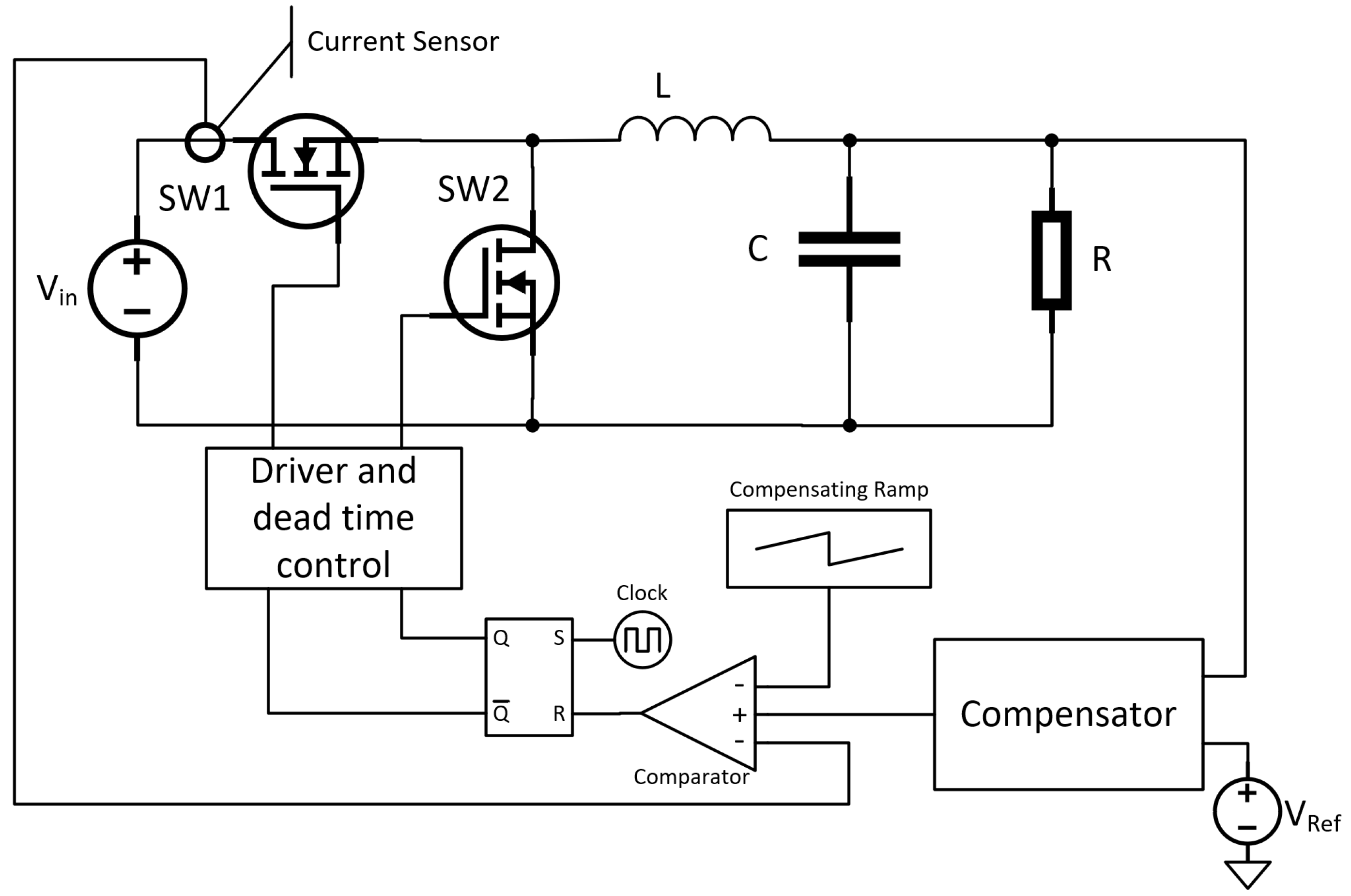
Figure 2.
Control signals of the buck converter under PCMC.

Figure 3.
The bifurcation map of the buck converter without compensation ramp. Vin = 6–12 V; Iref = 2–4 A; R = 2 Ω; L = 2.2 μH, C = 391 μF; f = 0.5 MHz, Sc = 0 V/s.
Figure 3.
The bifurcation map of the buck converter without compensation ramp. Vin = 6–12 V; Iref = 2–4 A; R = 2 Ω; L = 2.2 μH, C = 391 μF; f = 0.5 MHz, Sc = 0 V/s.

Figure 4.
The bifurcation diagrams for (a) Vin = 6 V and (b) Vin = 7 V (Iref = 2−4 A; R = 2 Ω; L = 2.2 μH, C = 391 μF; f = 0.5 MHz, Sc = 0 V/s). P1 stands for period-1 mode of operation, and P2 for period-2.
Figure 4.
The bifurcation diagrams for (a) Vin = 6 V and (b) Vin = 7 V (Iref = 2−4 A; R = 2 Ω; L = 2.2 μH, C = 391 μF; f = 0.5 MHz, Sc = 0 V/s). P1 stands for period-1 mode of operation, and P2 for period-2.

Figure 5.
Attractors for Vin = 6 V and (a) Iref = 3 A and (b) Iref = 3.5 A; for (a,b) R = 2 Ω; L = 2.2 μH, C = 391 μF; f = 0.5 MHz, Sc = 0 V/s.
Figure 5.
Attractors for Vin = 6 V and (a) Iref = 3 A and (b) Iref = 3.5 A; for (a,b) R = 2 Ω; L = 2.2 μH, C = 391 μF; f = 0.5 MHz, Sc = 0 V/s.

Figure 6.
The bifurcation map of the buck converter with compensation ramp. Vin = 6 V; Iref = 2–4 A; R = 2 Ω; L = 2.2 μH, C = 391 μF; f = 0.5 MHz, Sc = 0–2 × 10⁶ V/s.
Figure 6.
The bifurcation map of the buck converter with compensation ramp. Vin = 6 V; Iref = 2–4 A; R = 2 Ω; L = 2.2 μH, C = 391 μF; f = 0.5 MHz, Sc = 0–2 × 10⁶ V/s.

Figure 7.
The bifurcation diagrams for Sc = 0.2 × 10⁻⁶ V/s and Sc = 1 × 10⁶ V/s. Vin = 6 V; Iref = 2–4 A; R = 2 Ω; L = 2.2 μH, C = 391 μF; f = 0.5 MHz. P1 stands for period-1 mode of operation, P2 for period-2.
Figure 7.
The bifurcation diagrams for Sc = 0.2 × 10⁻⁶ V/s and Sc = 1 × 10⁶ V/s. Vin = 6 V; Iref = 2–4 A; R = 2 Ω; L = 2.2 μH, C = 391 μF; f = 0.5 MHz. P1 stands for period-1 mode of operation, P2 for period-2.

Figure 8.
The bifurcation diagram for Iref = 3.4 A. Vin = 6 V; R = 2 Ω; L = 2.2 μH, C = 391 μF; f = 0.5 MHz, Sc = 0–2 × 10⁶ V/s. P1 stands for period-1 mode of operation, and P2 for period-2.
Figure 8.
The bifurcation diagram for Iref = 3.4 A. Vin = 6 V; R = 2 Ω; L = 2.2 μH, C = 391 μF; f = 0.5 MHz, Sc = 0–2 × 10⁶ V/s. P1 stands for period-1 mode of operation, and P2 for period-2.

Figure 9.
CIP Hybrid Power Starter kit in peak-current-mode control configuration.

Figure 10.
Output voltage ripple measurement setup.

Figure 11.
Phase plot and autocorrelation function of the output voltage ripple ().

Figure 12.
Phase plot and autocorrelation function of output voltage ripple ().

Figure 13.
Phase plot and autocorrelation function of output voltage ripple ().

Figure 14.
Phase plot and autocorrelation function of output voltage ripple ().

Figure 15.
Efficiency measurement setup.

Figure 16.
The dependence of output voltage ripples on changes.

Figure 17.
The dependence of output voltage ripples on variation.

Figure 18.
Efficiency dependence on changes.

Figure 19.
Efficiency dependence on changes.


Table 1.
Parameters of the buck converter under test.
| Parameter | Values |
|---|---|
| Vin | 6…12 V |
| Iref | 2…4 A |
| R | 2 Ω |
| L | 2.2 μH |
| C | 391 μF |
| f | 0.5 MHz |
| Sc | 0 V/s |
Table 2.
The dependence of output voltage ripples on changes.
| Mean Output Voltage Ripples | |||||
|---|---|---|---|---|---|
| Vref (V)↓ | Vin = 6 V | Vin = 8 V | Vin = 10 V | Vin = 12 V | Period-1 |
| 2 | 3.90 | 4.10 | 4.32 | 9.42 | Period-2 |
| 2.1 | 4.03 | 4.38 | 4.35 | 10.51 | Period-4 |
| 2.2 | 4.41 | 4.68 | 4.80 | 4.28 | Period-N |
| 2.3 | 8.71 | 5.04 | 5.17 | 4.51 | Chaos |
| 2.4 | 8.71 | 5.36 | 5.59 | 5.03 | Uncertain regime |
| 2.5 | 10.60 | 5.77 | 5.96 | 5.55 | |
| 2.6 | 12.05 | 5.97 | 6.33 | 5.99 | |
| 2.7 | 15.95 | 6.37 | 6.78 | 6.48 | |
| 2.8 | 16.46 | 6.59 | 7.21 | 6.86 | |
| 2.9 | 18.07 | 6.98 | 7.66 | 7.50 | |
| 3 | 21.56 | 11.19 | 8.10 | 7.83 | |
| 3.1 | 20.78 | 12.75 | 8.62 | 8.41 | |
| 3.2 | 23.19 | 12.76 | 9.01 | 8.88 | |
| 3.3 | 25.22 | 15.62 | 9.45 | 9.46 | |
| 3.4 | 27.17 | 17.33 | 9.91 | 10.00 | |
| 3.5 | 28.73 | 19.87 | 10.29 | 10.57 | |
Table 3.
The dependence of output voltage ripples on changes.
| Vref Values (V) → | Mean Ripple Voltage Amplitude (Peak to Peak) for Parameters Rload − Vref (mV) | |||||
|---|---|---|---|---|---|---|
| Rload Values (Ω) → | 2 | 4 | 6 | 8 | 10 | |
| 2.5 | 3.83 | 2.97 | 3.07 | 2.84 | 2.91 | Period-1 |
| 2.9 | 4.83 | 3.85 | 2.90 | 3.63 | 3.60 | Period-2 |
| 3 | 11.36 | 4.16 | 3.94 | 3.84 | 4.13 | Period-N |
| 3.1 | 12.72 | 8.18 | 4.25 | 4.09 | 4.34 | Chaos |
| 3.2 | 13.20 | 12.92 | 4.38 | 4.30 | 4.50 | Uncertain regime |
| 3.3 | 15.70 | 12.64 | 22.21 | 30.49 | 4.87 | |
| 3.4 | 18.32 | 12.75 | 12.97 | 12.99 | 4.99 | |
| 3.5 | 19.08 | 12.64 | 13.07 | 12.84 | 13.06 | |
| 3.6 | 20.09 | 19.15 | 12.62 | 12.72 | 12.96 | |
| 3.7 | 25.86 | 21.74 | 12.71 | 12.72 | 12.76 | |
| 3.8 | 28.98 | 25.89 | 12.54 | 12.43 | 12.71 | |
Table 4.
Measurements data comparison to numerical analysis results.
| Vin = 6 V | ||
| Vref, V | Iref, A | Num. analysis mode |
| 2 | 2.13 | Period-1 |
| 2.4 | 2.82 | Period-2 |
| 2.7 | 3.02 | Period-N (Group 0) |
| 3.5 | 3.38 | Chaos |
| Vin = 8 V | ||
| Vref, V | Iref, A | Num. analysis mode |
| 2.5 | 2.70 | Period-1 |
| 3.2 | 3.72 | Period-2 |
| 3.5 | 3.93 | Period-N (Group 0) |
| 3.8 | 4.47 | Chaos |
| Vin = 10 V | ||
| Vref, V | Iref, A | Num. analysis mode |
| 2.2 | 2.51 | Period-1 |
| 2.6 | 2.92 | Period-1 |
| 3 | 3.29 | Period-1 |
| 3.5 | 3.72 | Period-2 |
Table 5.
Efficiency comparison for chaotic (PRG turned off) and period-1 (PRG turned on) modes ( group).
Table 5.
Efficiency comparison for chaotic (PRG turned off) and period-1 (PRG turned on) modes ( group).
| , Ω | , V | , A | , V | , A | , V | η, % | η, % (PRG Turned Off) | |
|---|---|---|---|---|---|---|---|---|
| With PRG turned on | 2 | 3.8 | 1.804 | 7.7172 | 2.593 | 5.0219 | 93.535% | 92.330% |
| 4 | 3.8 | 1.022 | 7.844 | 1.461 | 5.0175 | 91.443% | 89.077% |
Table 6.
Efficiency comparison for chaotic (PRG turned off) and period-1 (PRG turned on) modes ( group).
Table 6.
Efficiency comparison for chaotic (PRG turned off) and period-1 (PRG turned on) modes ( group).
| , Ω | , V | , A | , V | , A | , V | η, % | η, % (PRG Turned Off) | |
|---|---|---|---|---|---|---|---|---|
| With PRG turned on | 2 | 3.5 | 2.055 | 5.6817 | 2.385 | 4.6126 | 94.220% | 94.021% |
| 2 | 3.8 | 1.804 | 7.7172 | 2.593 | 5.0219 | 93.535% | 92.330% |
Disclaimer/Publisher’s Note: The statements, opinions and data contained in all publications are solely those of the individual author(s) and contributor(s) and not of MDPI and/or the editor(s). MDPI and/or the editor(s) disclaim responsibility for any injury to people or property resulting from any ideas, methods, instructions or products referred to in the content. |
© 2023 by the authors. Licensee MDPI, Basel, Switzerland. This article is an open access article distributed under the terms and conditions of the Creative Commons Attribution (CC BY) license (https://creativecommons.org/licenses/by/4.0/).
Share and Cite
MDPI and ACS Style
Tjukovs, S.; Surmacs, D.; Grizans, J.; Iheanacho, C.V.; Pikulins, D. Implementation of Buck DC-DC Converter as Built-In Chaos Generator for Secure IoT. Electronics 2024, 13, 20. https://doi.org/10.3390/electronics13010020
AMA Style
Tjukovs S, Surmacs D, Grizans J, Iheanacho CV, Pikulins D. Implementation of Buck DC-DC Converter as Built-In Chaos Generator for Secure IoT. Electronics. 2024; 13(1):20. https://doi.org/10.3390/electronics13010020
Chicago/Turabian StyleTjukovs, Sergejs, Daniils Surmacs, Juris Grizans, Chukwuma Victor Iheanacho, and Dmitrijs Pikulins. 2024. "Implementation of Buck DC-DC Converter as Built-In Chaos Generator for Secure IoT" Electronics 13, no. 1: 20. https://doi.org/10.3390/electronics13010020
Note that from the first issue of 2016, this journal uses article numbers instead of page numbers. See further details here.