Article

MeMPA: A Memory Mapped M-SIMD Co-Processor to Cope with the Memory Wall Issue

1
Department of Energy, Polytechnic of Turin, 10129 Turin, Italy
2
Department of Electronics and Telecommunications, Polytechnic of Turin, 10129 Turin, Italy
*
Author to whom correspondence should be addressed.
Electronics 2024, 13(5), 854; https://doi.org/10.3390/electronics13050854
Submission received: 25 January 2024 / Revised: 19 February 2024 / Accepted: 20 February 2024 / Published: 23 February 2024
(This article belongs to the Special Issue Advanced Memory Devices and Their Latest Applications)

Abstract

:
The amazing development of transistor technology has been the main driving force behind modern electronics. Over time, this process has slowed down introducing performance bottlenecks in data-intensive applications. A main cause is the classical von Neumann architecture, which entails constant data exchanges between processing units and data memory, wasting time and power. As a possible alternative, the Beyond von Neumann approach is now rapidly spreading. Although architectures following this paradigm vary a lot in layout and functioning, they all share the same principle: bringing computing elements as near as possible to memory while inserting customized processing elements, able to elaborate more data. Thus, power and time are saved through parallel execution and usage of processing components with local memory elements, optimized for running data-intensive algorithms. Here, a new memory-mapped co-processor (MeMPA) is presented to boost systems performance. MeMPA relies on a programmable matrix of fully interconnected processing blocks, each provided with memory elements, following the Multiple-Single Instruction Multiple Data model. Specifically, MeMPA can perform up to three different instructions, each on different data blocks, concurrently. Hence, MeMPA efficiently processes data-crunching algorithms, achieving energy and time savings up to 81.2% and 68.9%, respectively, compared with a RISC-V-based system.

1. Introduction

Electronic systems need more and more computational power to fulfill the increasing complexity of modern applications. Such applications, like Neural Networks, for example, require the execution of a vast number of instructions in parallel, implying stringent constraints on the design of application-specific accelerators or CPU-centric architectures. Nowadays, the von Neumann paradigm is the most diffused computing approach: it consists of a Central Processing Unit (CPU) and memory devices separated from each other, constantly exchanging information and data. The computational part is located in the CPU, which executes calculations by extracting data from memory and saving the results back into the memory itself. This organization achieves a high degree of flexibility and supports a wide variety of algorithms that can be easily written and compiled for such architectures. However, von Neumann’s architectures are affected by a huge bottleneck: the Memory Wall. CPUs are becoming more efficient and faster, but the memories cannot follow the same trend, implying a performance reduction [1]. Several approaches are proposed in the literature to solve this problem and belong to the Beyond von Neumann Computing (BvNC) category [2,3,4,5,6,7,8,9,10,11,12,13,14,15]. They consist of a completely new way of designing processing systems architectures that reduces the communication time and power overheads by either bringing memory and processing units as close as possible (Near-Memory computing) or implementing part of the computations directly inside the memory (In-Memory Computing). Usually, these solutions belonging to BvNC process data in parallel, concurrently to the CPU execution.
A brief but precise overview of the In-Memory paradigm, based on different technologies and structures, is presented in [16]. In some SRAM [3,4] and DRAM [5,6] solutions, by enabling multiple wordlines (WLs) at the same time, simple calculations are performed along the same bitline (BL). The resulting voltage potentials or currents on the BLs, proportional to the content of the cells, are sensed by the sense amplifiers designed to perform simple logical or multiply-and-accumulate (MAC) [7] calculations. In some works, few modifications of the original memory structure are made. In [17], the classical structure of the SRAM cell is modified by inserting a differential XNOR gate and an accumulation part. Other solutions are based on emerging resistive technologies that are gaining increasing importance in the In-Memory Computing paradigm. Belonging to this category is Resistive RAM (RRAM) [8,9], Magnetic Tunnel Junctions (MTJs) [10,11] and Phase-Change Memories (PCMs) [12,13]. These devices have different resistance states that can be programmed according to the applied voltage or current and associated with logic-0 and logic-1. They are organized in a crossbar structure in which the basic cells are composed of one-transistor-one-resistance (1T1R) devices. These cells are piloted by a WL and connected to a BL, in which the current is proportional to the resistance on the path, resulting in being very efficient for MAC-based applications.
Regarding the Near-Memory computing paradigm, some DRAM-based computing architectures focus on instantiating the computational elements very close to the memory, maintaining the memory array structure unaltered. In 3D Stacked RAMs [14] and Hybrid Memory Cubes [15], multiple layers of DRAM arrays are vertically stacked and connected to a computational layer employing Through Silicon Vias (TSVs). Another Near-Memory approach is exploited in GP-SIMD [18]. GP-SIMD consists of a regular CPU and a Single Instruction Multiple Data (SIMD) co-processor communicating with the same shared memory. With a collection of bit-serial processing units (PUs), each associated with a separate memory row, the SIMD co-processor physically lies near the memory array, thus forming a huge memory integrating computing capabilities. The PUs structure comprises one Full Adder, one logic block, and four registers. This structure recalls the one of the Field Programmable Gate Arrays (FPGAs) [19] and Coarse-Grained Reconfigurable Architectures (CGRAs) [20], known for their reconfigurability properties that allow for a high degree of programming flexibility. FPGA’s basic elements are the Configurable Logic Blocks (CLBs) that implement simple single-bit logic functions. CLBs are composed of Look-Up Tables (LUTs), sequential components, and small configuration memories. In order to obtain more complex functions, CLBs are connected together through complex configurable interconnection structures, degrading the performance. On the other hand, CGRAs rely on multiple-bit Reconfigurable Cells (RCs), organized in an interconnected mesh, that can perform more complex operations. RCs are generally composed of an Arithmetic Logic Unit (ALU), configuration registers, SRAMs, and multiplexers [20] supporting a higher level of granularity compared with FPGAs. A higher granularity lightens the impact of interconnections on the overall complexity and empowers programming flexibility, fitting a wider range of applications. In this work, we focus on the BvNC and CGRA concepts, presenting the Memory-Mapped Programmable Architecture (MeMPA) that is mainly intended as an architectural solution to cope with the Memory Wall issue, so it must be inserted in standard systems alongside the memory and the CPU. In particular, the contributions of this paper can be summarized as follows:
  • MeMPA design resumes from a previous work named Hybrid-SIMD [2]. The Hybrid-SIMD is a SIMD vectorial co-processor that combines memory and computational capabilities to reduce the Memory Wall overhead for highly parallel data-intensive applications. Yet, Hybrid-SIMD supports a small amount and very specific operations, essentially limited by the increasing complexity and performance degradation. Hence, the MeMPA co-processor was designed to improve the computing and programming capabilities by organizing the processing elements (PEs) in a matrix fashion instead of a vectorial one and accurately devising the PE’s internal structures.
  • The PE structure was derived by statistical analysis on different benchmarks consisting of profiling the algorithms and estimating the most recurrent instructions that were later integrated inside MeMPA.
  • The MeMPA concept stresses programming generality even more. Since the Hybrid-SIMD could not efficiently execute sequential portions of the algorithms because of its intrinsic structural limitations, the MeMPA PEs matrix was enriched with different programmable interconnections, drastically dropping the algorithm execution time and leading to significant energy savings.
  • To push even more toward a maximized parallel execution, the computing paradigm of the MeMPA co-processor was designed to refer to the Multiple-SIMD (M-SIMD) approach to enable the execution of different instructions on different datasets at the same time.
  • MeMPA was compared with Hybrid-SIMD in terms of execution time and energy for the same set of benchmarks used in [2] to demonstrate the improvements achieved by the MeMPA structure.
  • Finally, MeMPA was inserted inside a CPU-Memory context. Two systems were evaluated: CPU-Mem, based on a classical structure with a RISC-V core, and CPU-Mem-MeMPA, which considers the MeMPA insertion. In this work, other BvNC solutions presented in the literature are not considered as criteria for comparison because the attention is focused on the evaluation of the improvements of MeMPA with respect to Hybrid-SIMD and the MeMPA impact in a classical von Neumann CPU-Memory system.
The rest of the paper is organized as follows. Section 2 introduces the algorithm profiling procedure to design the PEs. Section 3 outlines the MeMPA structure. Section 4 reports the synthesis and Place&Route results. Section 5 explains the benchmarks mapping on MeMPA. Section 6 compares the accomplished performance with both the achievements of the Hybrid-SIMD and a standard CPU-Memory architecture, and finally Section 7 concludes the paper.

2. Algorithm Profiling

The starting point of the MeMPA architecture was the analysis of different algorithms to understand which type of basic operations are most common. SPLASH-2 benchmark suite [21] was considered, containing a set of complex and parallel algorithms typically used to evaluate the performance of CPU-centric architectures. In this analysis, each algorithm was profiled, estimating the type of instructions required and their occurrences so that then the instructions to be included in the MeMPA could be derived from the profiling outcomes. The goal was the creation of an architecture made of elements with both logic and memory capabilities so that the most used operations could be executed and the results written directly inside the PEs, reducing the number of accesses to the memory and thus increasing the efficiency of the algorithm execution. The following steps were followed to profile each algorithm:
  • Choose the reference Instruction Set Architecture (ISA). This paper used a RISC-V-based system, requiring cross-compiling the benchmarks for a RISC-V ISA. The RISC-V GNU Toolchain from [22] was configured with base integer, multiplication/division, and atomic extensions but not with the floating-point one since MeMPA architecture does not support floating-point calculations. The built toolchain was used to compile the benchmarks and generate the executable files.
  • Run the benchmarks and trace the algorithm execution. For these purposes, the Gem5 Simulator [23] was used in system-call emulation mode. Gem5 executes SPLASH-2 benchmarks with the instructions trace feature enabled. In this way, for each algorithm, the simulator prints a disassembled version, reporting the actual instructions executed by the core. These data are saved into a file named program.out.
  • Estimate the instructions occurrences. The program.out file was parsed by a Python script that counts the number of instructions for each algorithm. A final plot is shown in Figure 1, which considers all the instruction counts contributions of each benchmark in percentage. For example, considering the addi instruction, its value was obtained as the sum of the number of addi instructions for each benchmark (or test) divided by the total number of instructions of each benchmark (which is ∼64 M), following Equatiion (1).
    Instruction occurrence addi = i # tests ( # addi i ) # instructions × 100 %
By analyzing the results in Figure 1, the most frequently used instructions are arithmetical (addi, add, mul, subw, and sub, etc.) and logical (srli, slli, andi, or, etc.). From these data, a possible subset of hardware blocks to be inserted in MeMPA was defined. In this way, a significant part of the CPU computations can be moved directly inside the MeMPA co-processor, enabling the BvNC paradigm. Moreover, Figure 1 also shows a significant contribution of the memory operations (sd, ld), confirming once again the strong impact of the von Neumann Bottleneck on standard systems.

3. Architecture

3.1. System Overview

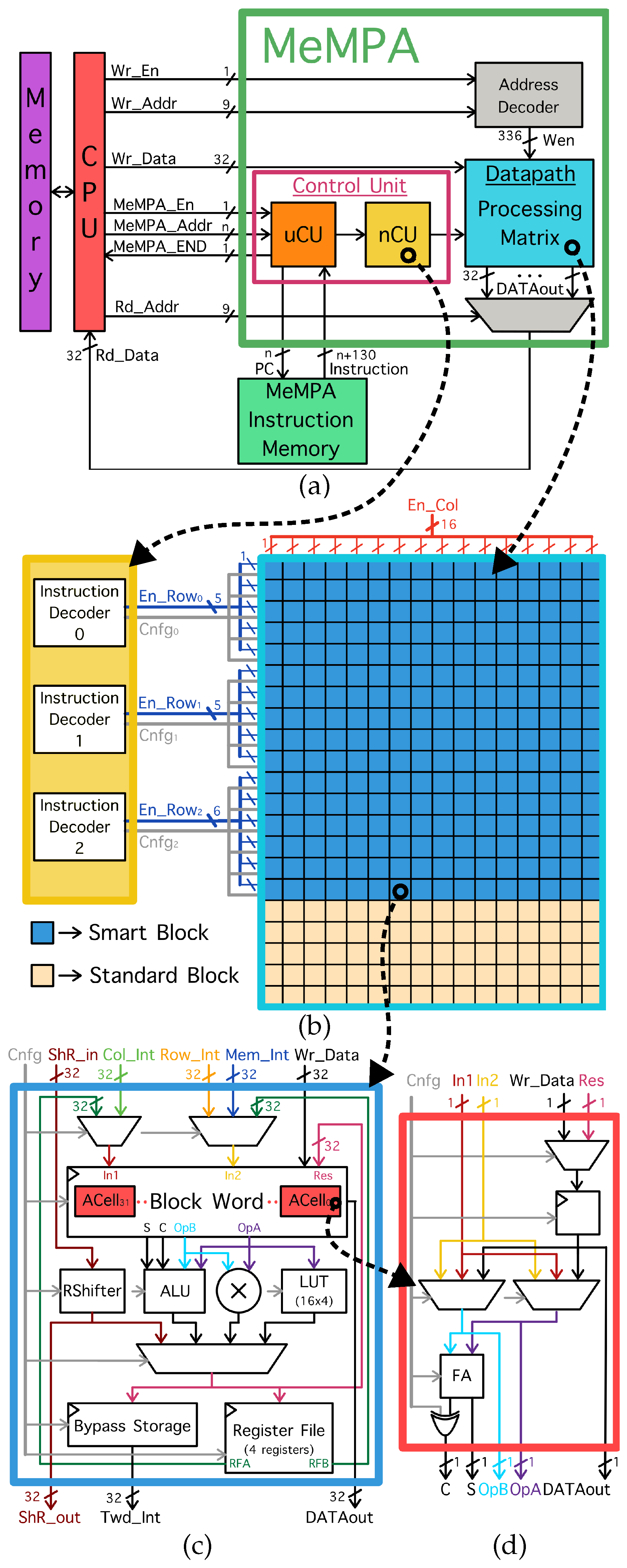
In Figure 2a, the system environment hosting the MeMPA is shown.
Since MeMPA acts as a memory-mapped co-processor, the CPU needs at its interface two sets of signals to correctly interact with MeMPA: one for exchanging data and another for starting MeMPA to run the data-intensive portions of the code loaded inside the MeMPA Instruction Memory. In particular, the former set leverages the standard double port data memory protocol (one asynchronous reading port and one synchronous writing port), including the signals: Wr_En, which enables to store the data passed through the Wr_Data signal inside the MeMPA PE addressed by the Wr_Addr signal, and  Rd_Addr, which contains the address of the PE from which the CPU must read the data, then forwarded by the Read_Address signal. Instead, the latter set includes three signals, which are: the MeMPA_En signal, sent by the CPU to enable MeMPA running the algorithm stored in the MeMPA Instruction Memory starting from the address specified by the MeMPA_Addr signal, and the MeMPA_END signal that is asserted by MeMPA when it terminates the algorithm execution and the results are ready and available inside the PEs matrix. To properly handle all these signals, especially for the second set, the ISA of the CPU must be customized by inserting a few specific instructions. Furthermore, MeMPA needs at its interface two more signals to asynchronously fetch from the MeMPA Instruction Memory the operations it has to perform, i.e., the PC signal, which is used to forward the address of the next instruction to be executed, and the Instruction signal, which holds the content of the instruction pointed.
Concerning the internal structure of MeMPA, it is composed of three macro sections: the control section, the datapath, given by the matrix of fully interconnected PEs (i.e., the Processing Matrix) that is where the data elaboration inside MeMPA occurs, and the section to handle the data exchange with the CPU. This last section connects the first set of CPU external pins with the Processing Matrix through an address decoder and a multiplexer used to select the PE where the data must be written or read, respectively.
The control part is composed of two control units connected in sequence: the micro Control Unit (uCU), which is a micro-programmed machine [2] that regulates the instruction flow inside MeMPA, and the nano Control Unit (nCU), which works like a standard instruction decoder. The nCU translates the instruction withdrawn by the uCU from the MeMPA Instruction Memory into configuration signal values that control the data elaboration performed across the datapath. The uCU, nCU, and datapath are interleaved with pipeline registers, so splitting the MeMPA elaboration process into four stages: fetch, decode, execute, and write back. While the last two phases are performed inside the datapath, the first and second ones are associated with the uCU and the nCU, respectively.
The datapath is represented by the Processing Matrix, which is the entity of MeMPA that handles the data storage and elaboration. The Processing Matrix is made up of 256 PEs with memory capabilities, called Smart Blocks, organized in an array of 16 columns and 16 rows. In addition, below this block, a set of 80 Standard Blocks, which are standard registers that provide MeMPA with further storage space, is placed as shown in Figure 2b. During the algorithm execution, all the 256 Smart Blocks process in parallel 32-bit data and are driven by the Control Unit so as to implement the MeMPA processing according to the M-SIMD computing paradigm. Due to the nCU structure, which is composed of three instruction decoders, the Processing Matrix is enabled to run up to three different instructions, each on a different set of data, simultaneously. In particular, each instruction decoder (ID) takes as input a different sub-portion of the MeMPA instruction and translates it into control signals driving a specific set of Smart Block rows. This means that Smart Blocks connected to the same ID execute the same instruction at the same time. Figure 2b illustrates the association between IDs and Smart Block sets.
Furthermore, it is also possible to partially specify which are the Smart Blocks that need to be active for the execution of the currently demanded operations. In order to make a trade-off between the instruction length and the programming flexibility, given by reserving 256 bits of the instruction for the enabling signals (1 for each Smart Block), the mesh-like arrangement of the Processing Matrix is exploited to implement a battleship game-like enabling mechanism. In the instruction, 32 bits are dedicated for the enabling signals, of which 16 are for the activation of the Smart Block columns and 16 for the Smart Block rows (one enable signal drives all Smart Blocks on the same column or row), as shown in Figure 2b. It follows that each Smart Block is connected to two enable signals; thus, if one of them is not active, that Smart Block is disabled.

3.2. Datapath: The Processing Matrix

The Processing Matrix is the core of the MeMPA paradigm, characterized by the extensive interaction between the Smart Blocks and a complex network of interconnections that routes the Processing Matrix itself, enabling an efficient and programmable data exchange across the whole array.

3.2.1. Routing Network

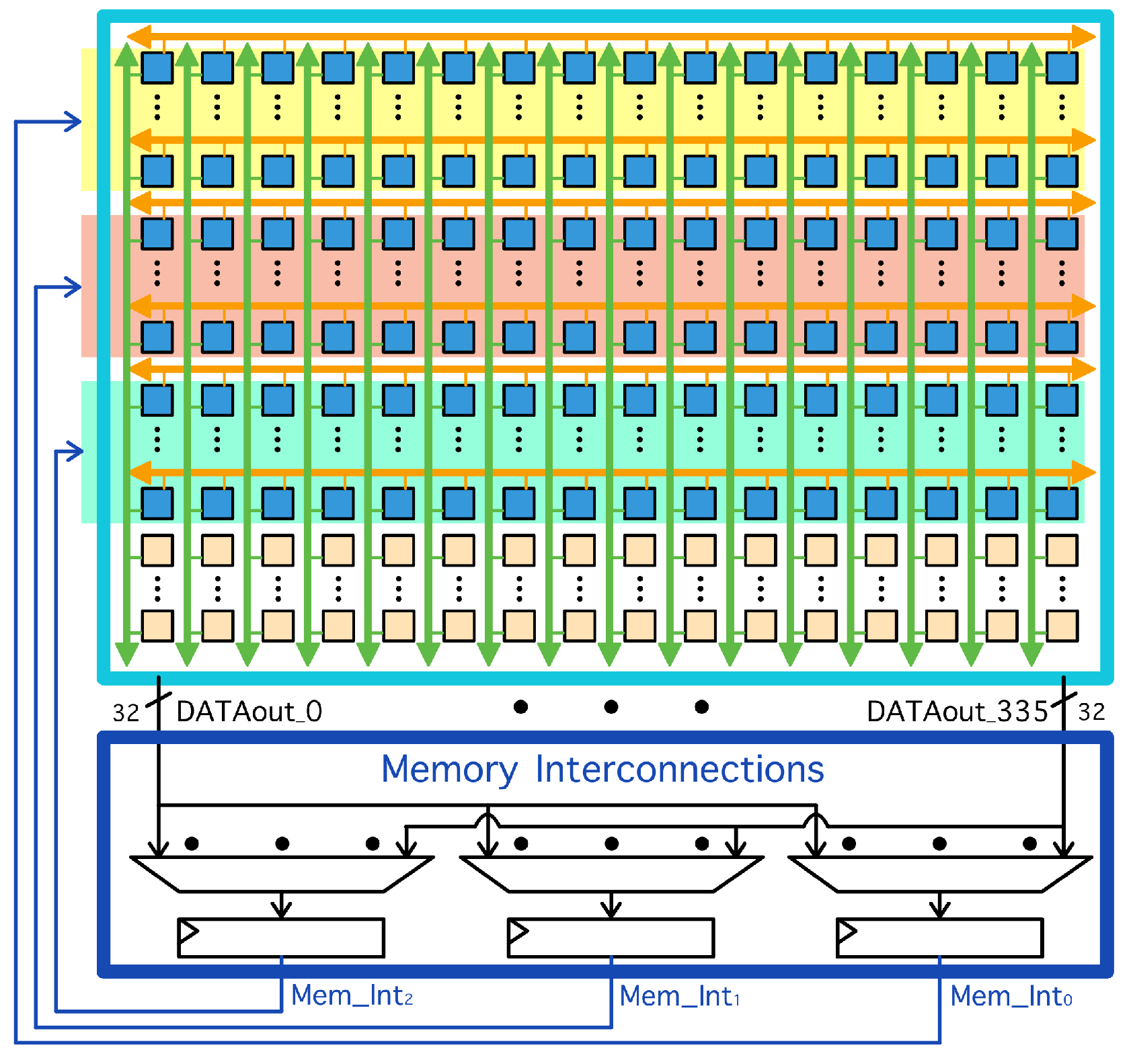
The routing network comprises two different kinds of interconnections: the Memory Interconnections and the Reduction Tree Interconnections. Looking at Figure 3, the orange and green arrows identify the Row and Column Interconnections, respectively, that belong to the second type, while the blue box refers to the Memory Interconnections. All of them are implemented through a proper organization of several multiplexers. On the one hand, each Row Interconnection enables the data transfer among the Smart Blocks on the same row, while each Column Interconnection, stretching over the Standard Blocks too, allows the Smart Blocks to take data from any of the blocks placed along the same column. On the other hand, the Memory Interconnections extend all over the Processing Matrix so that each Smart Block can retrieve the data from any block. However, the two types of interconnections do not stand out for the set of blocks they link but rather differ in how they distribute the data among the different blocks. Each Row or Column Interconnection allows all the attached Smart Blocks to take simultaneously one different data, even if the same instruction drives them, while the Memory Interconnections are used when Smart Blocks controlled by the same instruction all need to pick the same data coming from an arbitrary block of the Processing Matrix. Particularly, the Reduction Tree Interconnections are one of the key points of MeMPA since they are used to perform iterative operations on N data, such as maximum search, summations, etc., following a reduction tree mechanism that allows to reduce the number of the single operations encoding the iterative computation from N − 1 to log2N operations. Let us suppose to execute a summation on the values stored in the Smart Blocks of a generic row, connected through a Row Interconnection. By specifying the address ‘1’, the Row Interconnection provides as input to each Smart Block the content of the Smart Block on the right, while specifying the address ‘2’, the data forwarded to each block corresponds to the one held by the block two positions away on the right and so on for all the column composing one row. In this way, the summation on eight values: i = 1 8 x i can be implemented in three steps. In the first step, s 1 = x 1 + x 2 , s 2 = x 3 + x 4 , s 3 = x 5 + x 6 , and  s 4 = x 7 + x 8 are computed in parallel, while the second step performs s 5 = s 1 + s 2 and s 6 = s 3 + s 4 , and the third step terminates the processing evaluating s 5 + s 6 . Similarly to the Row Interconnections, the Column Interconnections allow the implementation of the same data exchange, i.e., if the address ‘1’ is specified, all the Smart Blocks on the same columns take the data coming from the block below them.

3.2.2. Smart Block

Diving deeper into the MeMPA Processing Matrix, the Smart Blocks assume a central role in the calculations. Each Smart Block (see Figure 2c) contains all the storage elements and computational blocks needed to implement the most common operations identified by the Algorithm Profiling procedure explained in Section 2. Inside a Smart Block, there is a Right Shifter (RShifter) to perform division-by-two, an ALU to implement most common arithmetic-logic operations, a multiplier, a Register File to hold temporary values, a Bypass Storage to provide the input data for the Reduction Tree Interconnections (through the Twd_Int signal), some multiplexers to select the data, a programmable Look-Up Table (LUT) with 16 4-bit entries, configured due to a Daisy Chain connection mechanism, to implement configurable customized functions, and a Block Word macro component. The Block Word is made of 32 1-bit arithmetic cells, shown in Figure 2d, which are the finer-grained entities of the MeMPA Processing Matrix, provided with both memory and processing capabilities. The arithmetic cells cope with ALU, Multiplier, and LUT to deliver the correct operand or to perform some preliminary logic operations (i.e., bitwise operations). In particular, through the cascade connection between Block Word and ALU, the following operations are implemented: not, and, nand, or, nor, xor, xnor, abs, +, , >, <, =, !=.
Moreover, the Block Word output is directly connected to the Memory Interconnections input through the DATAout signal. The Block Word is the only storage element the CPU can interact with, performing data writing or reading operations (through Wr_Data and DATAout signals) solely before the algorithm execution starts or after its termination.
For a generic operation, the Smart Block can work on data held by the Smart Block itself, inside the Block Word or the Register File, or coming from a block on the same row (Row_Int), a block on the same column (Col_Int), and an arbitrary block inside the Processing Matrix (Mem_Int). To enable MeMPA to execute a finite set of divisions by powers of 2, the RShifter has a separated input (ShR_in) in order to allow the cascade connections of all the RShifters belonging to the Smart Blocks on the same row (ShR_out signal coming out from the RShifter of the row first Smart Block connected to the ShR_in of the row second Smart Block, and so on). In this way, the Processing Matrix can perform up to 16 divisions in parallel on data coming from either Memory or Reduction Tree Interconnections.

3.3. Instructions Organization

The MeMPA instruction is subdivided into two macro fields called uInstruction and VLIW_Instruction, which are elaborated by the uCU and the nCU, respectively. The uInstruction comprises 5 + n bits (with n equal to the size of the address signal of the MeMPA Instruction Memory) encoding the information on the instruction flow to be followed, while the VLIW_Instruction (125 bits) provides all the details on which operations MeMPA has to execute on which data. Then, the first 16 bits of the VLIW_Instruction are reserved to the enable signals of the Processing Matrix columns, while the remaining bits are divided into other three macro-fields of 36, 36, and 37 bits that feed the first, second and third IDs, respectively, encoding all the different operations that MeMPA can simultaneously execute through the Smart Blocks. In turn, each of these macro-fields is split into the following eight fields:
  • EN_ROW: contains the enabling signals (En_Row) of the Processing Matrix rows as shown in Figure 2b;
  • OPCODE: tells whether the operation to be performed is a load or an arithmetical one and, in this last case, specifies by which of the arithmetic-logic blocks, among RShifter, ALU, Multiplier, and LUT, that operation has to be carried out;
  • SOURCE_OP: selects which is the operand or couple of operands and their order for the required operation processing, choosing among data coming from Column Interconnections, Row Interconnections, Memory Interconnections, Register File, or Block Word;
  • DEST_OP: indicates where the operation result should be stored in the Smart Block among Block Word, Bypass Storage, and Register File;
  • ADDR_S1: specifies the address of the data to be elaborated when one of the operands selected through the SOURCE_OP field comes from the Column Interconnections, or the first output port of the Register File (RFA);
  • ADDR_S2: specifies the address of the data to be elaborated when one of the operands selected through the SOURCE_OP field comes from the Row Interconnections, the Memory Interconnection, or the second output port of the Register File (RFB);
  • ADDR_D: complements the DEST_OP field in case the Register File is selected as destination storage, holding the specific address of the register involved;
  • FUNC: is used to further detail which among the operations implemented by the arithmetic-logic block selected through the OPCODE field has to be performed.

4. Performance

MeMPA was synthesized with the CMOS 45 nm NanGate OpenCell Library using the Synopsys Design Compiler. The clock gating technique was inferred during the process to reduce the dynamic power consumption. After synthesis, the design was placed and routed using Cadence Innovus following a congestion-driven approach. Place&Route allows for estimating more reliable performance values since the results take into account more accurate models of the interconnections and parasitic elements inside the design. Due to the circuit complexity, the design was not flattened, meaning that the hierarchy of the blocks was maintained in the processes. The performance achieved after the Place&Route are:
  • Area occupation: 1.55 mm2.
  • Maximum clock frequency (fclk): 257.77 MHz.
  • Worst-case power: 670.48 mW @fclk = 250 MHz.
These results were obtained with the fixed dimensions of 16 × 16 Smart Blocks and 5 × 16 Standard Blocks with an M-SIMD degree of 3, defined by the number of IDs. However, the performance is strictly related to MeMPA scalability, meaning that, on the one hand, increasing the total number of Smart Blocks, Standard Blocks, their parallelism, or the degree of M-SIMD empowers the computing capability. On the other hand, exceeding the MeMPA sizing worsens key figures of merits like area, power, timing, and energy. Although it would have been interesting to evaluate the scaling trend thoroughly, due to the MeMPA complexity and the computing effort this analysis would have required, the scaling study was not performed, as it was beyond the scope of this article.

5. Benchmarks Mapping

To have straightforward esteem of the performance goodness achieved by MeMPA, we decided to map on the architecture the same benchmarks used for the Hybrid-SIMD evaluation [2], i.e., K-Nearest Neighbor (K-NN), K-means, Matrix-Vector Multiplication (MVM), Mean and Variance ( μ & σ 2 ), and Discrete Fourier Transform (DFT). Moreover, because of the lack of a real compiler for MeMPA, we excluded implementing the same SPLASH-2 algorithms used for the profiling procedure in Section 2, for which a manual mapping would have been extremely hard. Table 1 sums up the algorithms mapping in terms of number of processed data, number of clock cycles needed for the algorithm execution, and related power consumption.
For the sake of brevity, in the following, only the mapping of one among the implemented algorithms is detailed. In particular, the MVM mapping is provided for a two-fold reason. On the one hand, the MVM allows us to easily point out how the MeMPA highlights, as reduction tree mechanism, M-SIMD computing paradigm, and battleship game-like enabling mechanism, can be exploited to efficiently execute an application. On the other hand, it represents the operation at the base of convolutional neural networks that belong to the set of data-intensive applications that would heavily benefit from MeMPA usage in terms of time and energy consumption. However, the implementation of all other algorithms can be derived following along the same line as the implementation described for the MVM.

MVM

The mapping of any algorithm on MeMPA is given by two macro phases: the Processing Matrix initialization phase, where the CPU loads inside the Processing Matrix all data to be elaborated, and the algorithm execution phase, where the algorithm execution actually takes place.
Concerning the MVM described in Table 1, the implemented multiplication was performed between a 16 × 16 matrix and a 16 × 1 vector. Thus, during the Processing Matrix initialization phase, each of the matrix elements was stored inside a different Block Word of the Smart Blocks, while all the vector items were loaded inside the first row of Standard Blocks. The whole Processing Matrix initialization phase took 272 clock cycles, namely, one clock cycle for each data writing.
Then, one instruction was instantiated (one clock cycle) to perform the backup of the Block Words data into the first location of the Register Files, a step that is always needed for any algorithm in order to avoid losing the initial data when, at the end of the algorithm, the MeMPA saves the results into the Block Words to make them visible to the CPU.
Afterward, the real algorithm execution phase began by carrying out the 256 products between each matrix element ( x i , j ) and the right vector item ( y j ) needed for the computation of the final vector elements z i = j = 0 15 x i , j y j . In total, 5 + 1 instructions (six clock cycles) were used to fulfill these multiplications. In particular, for the first five instructions, all IDs were active, each driving only one Smart Blocks row at a time. A scheme of the first VLIW_Instruction is reported Figure 4.
Through this instruction, 1st, 6th, and 11th Smart Block rows were driven to compute all the x i , j · y j (with i = 0, 5, 10 and j = 0, …, 15) terms in parallel and save the outcome in the associated Bypass Storages. In more detail, looking at the structure of the first instruction in Figure 4, it can be seen that for ID1 (i.e., the first group of five Smart Block rows starting from the top in the diagram in Figure 2b), the activation pattern sees only the first row of Smart Blocks enabled, while the others are not (EN ROW = “10000”). The operation performed is a multiplication (OPCODE = Multiplier), having the data from the Column Interconnection and the Block Word as source operators (SOURCE OP = Col_Int_Block_Word). The data from the Column Interconnection are specified in the ADDRESS S1 field, which represents the address offset value from the first Smart Block belonging to the group. In this case, being the first group of Smart Blocks, the offset will be equal to 16, which is the sixteenth row of the Processing Matrix (corresponding to the first row of Standard Blocks). Finally, the destination is simply specified in the DEST OP field as Bypass, wanting to save the data in Bypass Storages. The same reasoning can be applied to ID2, which identifies the second group of Smart Blocks, also arranged in five rows. Again, the EN ROW is equal to “10000” identifying only the first row of the subgroup; the operation is always the multiplication (OPCODE = Multiplier); the source operands always coming from the Column Interconnections and the Block Words (SOURCE OP = Col_Int_Block_Word); the destination always Bypass Storages (DEST OP = Bypass), while the offset this time is equal to 11, always pointing to the first row of Standard Blocks.
Exploiting the same rationale, second, third, fourth, and fifth instructions computed the x i , j · y j terms for i equal to (1,6,11), (2,7,12), (3,8,13), and (4,9,14), respectively. Lastly, the sixth instruction performed the x 15 , j y j products by enabling only the last Smart Blocks row through the third instruction decoder.
Once all the products were ready inside the Bypass Storages of the Processing Matrix, all the sums generating the z i values were carried out in four instructions (four clock cycles). In order to carry this out, the reduction tree mechanism implemented due to the Row Interconnections was thoroughly exploited, allowing the reduction in the number of instructions needed for computing the 16 parallel summations from 15 to 4 instructions. The scheme of the first of these four instructions is shown in Figure 4 (Instruction 8). Differently from the previous set of instructions, where all the enable signals for the Smart Block columns were always active, each of these four instructions activated a different set of Smart Block columns, while all the IDs drove all the Smart Block rows with the same operation for the current clock cycle. For the first instruction, all the odd Smart Block columns were enabled so that all the following sums were computed and saved in the Bypass Storages: x i , 0 y 0 + x i , 1 y 1 , x i , 2 y 2 + x i , 3 y 3 , x i , 4 y 4 + x i , 5 y 5 , x i , 6 y 6 + x i , 7 y 7 , x i , 8 y 8 + x i , 9 y 9 , x i , 10 y 10 + x i , 11 y 11 , x i , 12 y 12 + x i , 13 y 3 , x i , 14 y 14 + x i , 15 y 15 , for i = 0, …, 15. Then, for the second instruction only columns 1, 5, 9, and 13 were enabled to compute the x i , 0 y 0 + x i , 1 y 1 + x i , 2 y 2 + x i , 3 y 3 , x i , 4 y 4 + x i , 5 y 5 + x i , 6 y 6 + x i , 7 y 7 , x i , 8 y 8 + x i , 9 y 9 + x i , 10 y 10 + x i , 11 y 11 , x i , 12 y 12 + x i , 13 y 3 + x i , 14 y 14 + x i , 15 y 15 terms, respectively. Similarly, the third and fourth instructions implemented the remaining sums so that, after the end of the last instruction, all the final z i values were available in the Block Words of the first Smart Blocks column.

6. Performance Comparisons on Benchmarks

In this section, the impact of the benchmarks in Table 1 is evaluated on MeMPA. Firstly, a comparison of energy and execution time between MeMPA and Hybrid-SIMD is presented. Both solutions consider two figures of merit: total execution time and energy (obtained as Power × Total Execution Time ). Since the Hybrid-SIMD has size and memory space that change according to the implemented algorithm, the energy and execution time used to compare the MeMPA performances with the Hybrid-SIMD ones are normalized by the number of samples considered for each algorithm (# Samples) for a fairer comparison. Secondly, and most importantly, MeMPA is inserted in classical CPU-Memory architecture, and the performance of the algorithms is evaluated in two distinct cases. In the first one, named CPU-Mem, the structure of the von Neumann architecture is kept unaltered, so the algorithms are entirely executed by the CPU and evaluated considering a classical context. The second one, CPU-Mem-MeMPA, considers the insertion of MeMPA inside the von Neumann architecture. In this case, the CPU, instead of running the entire algorithms, simply conveys data from memories into MeMPA, which is in charge of executing all the computations. By delegating the calculations to MeMPA, execution time and energy are reduced because of the parallelization of the algorithms performed by MeMPA, but also because of an overwhelming reduction in the memory accesses that waste a considerable amount of energy.

6.1. MeMPA vs. Hybrid-SIMD

The execution time and energy comparisons between MeMPA and Hybrid-SIMD are presented in Figure 5. Results are obtained after post-Place&Route simulation and back-annotation processes for both architectures. In particular, the values for Hybrid-SIMD and MeMPA are obtained with a clock period of 12ns and 4ns, respectively. The number of samples normalizes these evaluations to consider the complexity gap between the two solutions. Considering, for instance, the K-NN benchmark, Hybrid-SIMD processes 256 couples of coordinates (xi,yi) while MeMPA only 160. MeMPA has a smaller addressable space, meaning that a smaller number of data can be processed compared with Hybrid-SIMD. The smaller memory size of MeMPA is compensated by its high degree of programmability and capability to execute different complex operations concurrently. The architectural model of Hybrid-SIMD can implement a smaller set of algorithms with limited flexibility, which is especially exacerbated in sequential algorithms. As confirmed in Figure 5, MeMPA outperforms Hybrid-SIMD for all the proposed benchmarks in terms of execution time and energy. Moreover, MeMPA has both lower critical path (3.88 ns vs. 6.79 ns) and power (worst case: 102.18 mW, reference Table 1 vs. 212.90 mW for DFT algorithm) than the Hybrid-SIMD.

6.2. RISC-V with Normal Memory

This part presents a comparison in terms of energy and execution time between CPU-Mem and CPU-Mem-MeMPA frameworks. The CPU-Mem system is made of a RISC-V core with two levels of caches. Level 1 (L1) is divided into instruction and data caches having a size of 64 kB each, while Level 2 (L2) is a shared cache of 256 kB. The following steps were followed to estimate the consumption of the memories:
  • Implementation of the algorithms in C. CPU-Mem solution implements the whole algorithm in the core, while CPU-Mem-MeMPA simply conveys data from caches inside MeMPA sequentially.
  • Compilation of the benchmarks with RISC-V GNU Toolchain and simulation with Gem5. The CPU is an In-Order model (TimingSimpleCPU) that runs in the system call-emulation mode.
  • Analysis of stats.txt output file. At the end of the Gem5 simulation, an output file is generated containing statistics like the number of memory accesses for each cache, the total number of executed instructions, etc.
  • Memory consumption estimation with Cacti by HP [24]. Cacti is a tool able to model caches very precisely. It outputs parameters like the energy/access, starting from some essential memory characteristics (e.g., the size, the memory type, the associativity, the technology node, etc.). The memory consumption is simply obtained by multiplying the energy/access for each memory by the total accesses to that memory. This last information is stored inside stats.txt.
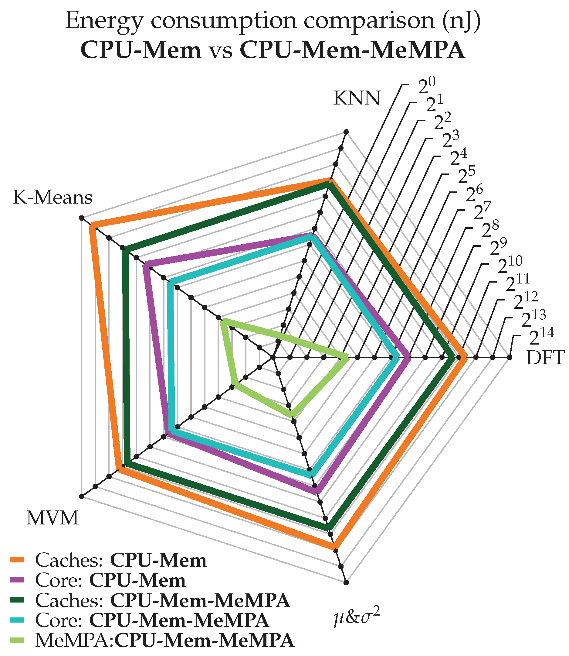
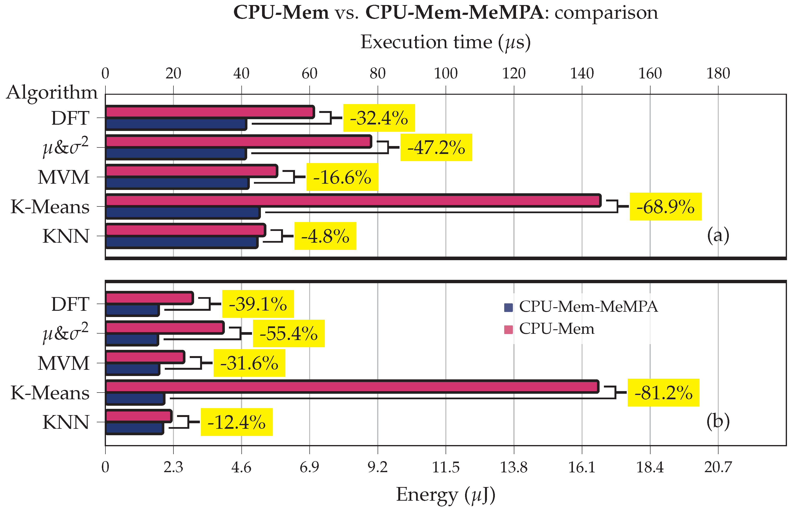
Moreover, an RTL model from the literature, i.e., the Pulpino In-Order single-core 4-stage pipeline RISC-V [25], was used to precisely estimate the RISC-V core performance. The core was synthesized and Place&Routed following the same methodology described for MeMPA. At the end of the Place&Route phase, the algorithms were simulated, and the core signals were back-annotated for power estimation with Cadence Innovus. The results are reported in Figure 6 and Figure 7, obtained with a clock period fixed to the worst critical path value between MeMPA and the RISC-V core, which is 6ns. In all benchmarks, the CPU-Mem-MeMPA framework outperforms the standard CPU-Mem in execution time and energy. Thanks to the M-SIMD computing mode of MeMPA and the dense interconnections network, the algorithms can be easily accelerated, reaching better performance, especially in parallel algorithms like K-Means or in algorithms allowing to heavily exploit the Reduction Tree computing mechanism like μ & σ 2 . It is essential to underline that the insertion of MeMPA also reduces the memory accesses and their energy because once data are loaded inside MeMPA, the computation is performed directly inside the Processing Matrix, as confirmed in Table 2 and Figure 6.
Data can be read from MeMPA once the algorithm is completed, reducing energy, execution time, and memory accesses up to ∼81.2%, 68.9% and 83.6%, respectively, for the K-Means algorithm.

7. Conclusions

In this paper, we proposed MeMPA, an M-SIMD co-processor designed to address the Memory Wall Issue. The MeMPA paradigm belongs to the BvNC category and focuses on a heavy parallelization, on different levels, of the algorithm execution to drastically cut off time and energy consumption. Moreover, the core part of MeMPA processing was designed to provide as much programming generality as possible by considering a wide range of algorithms from the SPLASH-2 benchmark suite and profiling the most used instructions. Due to its fully interconnected structure of processing elements integrating computing and storage capabilities, the insertion of MeMPA inside a classical CPU-Memory context was confirmed to successfully bring overwhelming reductions in energy and execution time up to 81.2% and 68.9% for the proposed benchmarks compared with the classical von Neumann solution. The concept of MeMPA is that of an architectural design that sees the merging of memory with computational elements, thus aiming to break down the von Neumann bottleneck. Data-intensive communications between processor and memory, in fact, have an extremely negative impact on performance, increasing execution time and consequently energy. In fact, memories, being slower than processors, introduce an overhead on access times, in fact most of the time the processor is waiting for data from the memory itself. With MeMPA as a coprocessor, being a mixed computation framework, the idea is to locate the computation units in memory, thus relaxing the classical von Neumann system and moving some of the computation within the MeMPA framework. As a future work, we aim to develop a complete toolchain made of a compiler that, starting from a generic code, can automatically map the algorithm on MeMPA to fully take advantage of the CPU-MeMPA interaction to perform more complex applications.

Author Contributions

Conceptualization, A.G.; methodology, A.G., A.C. and M.V.; validation, A.G. and A.C.; formal analysis, A.C.; investigation, A.G.; data curation, F.R.; writing—original draft preparation, A.C. and A.G.; writing—review and editing, M.V. and G.T.; visualization, F.R. and M.G.; supervision, M.V.; project administration, M.Z. All authors have read and agreed to the published version of the manuscript.

Funding

This research received no external funding.

Data Availability Statement

Data are contained within the article.

Conflicts of Interest

The authors declare no conflicts of interest.

References

  1. Hennessy, J.L.; Patterson, D.A. Computer Architecture: A Quantitative Approach; Elsevier: Amsterdam, The Netherlands, 2017. [Google Scholar]
  2. Coluccio, A.; Casale, U.; Guastamacchia, A.; Turvani, G.; Vacca, M.; Roch, M.R.; Zamboni, M.; Graziano, M. Hybrid-SIMD: A Modular and Reconfigurable approach to Beyond von Neumann Computing. IEEE Trans. Comput. 2021, 71, 2287–2299. [Google Scholar] [CrossRef]
  3. Akyel, K.C.; Charles, H.P.; Mottin, J.; Giraud, B.; Suraci, G.; Thuries, S.; Noel, J.P. DRC 2: Dynamically Reconfigurable Computing Circuit based on memory architecture. In Proceedings of the 2016 IEEE International Conference on Rebooting Computing (ICRC), San Diego, CA, USA, 17–19 October 2016; IEEE: Piscataway, NJ, USA, 2016; pp. 1–8. [Google Scholar] [CrossRef]
  4. Lin, Z.; Zhan, H.; Li, X.; Peng, C.; Lu, W.; Wu, X.; Chen, J. In-Memory Computing with Double Word Lines and Three Read Ports for Four Operands. IEEE Trans. Very Large Scale Integr. (VLSI) Syst. 2020, 28, 1316–1320. [Google Scholar] [CrossRef]
  5. Ali, M.F.; Jaiswal, A.; Roy, K. In-Memory Low-Cost Bit-Serial Addition Using Commodity DRAM Technology. IEEE Trans. Circuits Syst. I Regul. Pap. 2019, 67, 155–165. [Google Scholar] [CrossRef]
  6. Seshadri, V.; Lee, D.; Mullins, T.; Hassan, H.; Boroumand, A.; Kim, J.; Kozuch, M.A.; Mutlu, O.; Gibbons, P.B.; Mowry, T.C. Ambit: In-memory accelerator for bulk bitwise operations using commodity DRAM technology. In Proceedings of the 2017 50th Annual IEEE/ACM International Symposium on Microarchitecture (MICRO), Cambridge, MA, USA, 14–18 October 2017; IEEE: Piscataway, NJ, USA, 2017; pp. 273–287. [Google Scholar] [CrossRef]
  7. Jaiswal, A.; Chakraborty, I.; Agrawal, A.; Roy, K. 8T SRAM cell as a multibit dot-product engine for beyond von Neumann computing. IEEE Trans. Very Large Scale Integr. (VLSI) Syst. 2019, 27, 2556–2567. [Google Scholar] [CrossRef]
  8. Wang, H.; Yan, X. Overview of resistive random access memory (RRAM): Materials, filament mechanisms, performance optimization, and prospects. Phys. Status Solidi (RRL)-Rapid Res. Lett. 2019, 13, 1900073. [Google Scholar] [CrossRef]
  9. Kvatinsky, S.; Belousov, D.; Liman, S.; Satat, G.; Wald, N.; Friedman, E.G.; Kolodny, A.; Weiser, U.C. MAGIC—Memristor-aided logic. IEEE Trans. Circuits Syst. II Express Briefs 2014, 61, 895–899. [Google Scholar] [CrossRef]
  10. Durlam, M.; Naji, P.; DeHerrera, M.; Tehrani, S.; Kerszykowski, G.; Kyler, K. Nonvolatile RAM based on magnetic tunnel junction elements. In Proceedings of the 2000 IEEE International Solid-State Circuits Conference. Digest of Technical Papers (Cat. No. 00CH37056), San Francisco, CA, USA, 9 February 2000; IEEE: Piscataway, NJ, USA, 2000; pp. 130–131. [Google Scholar] [CrossRef]
  11. Rakin, A.S.; Angizi, S.; He, Z.; Fan, D. Pim-tgan: A processing-in-memory accelerator for ternary generative adversarial networks. In Proceedings of the 2018 IEEE 36th International Conference on Computer Design (ICCD), Orlando, FL, USA, 7–10 October 2018; IEEE: Piscataway, NJ, USA, 2018; pp. 266–273. [Google Scholar] [CrossRef]
  12. Sebastian, A.; Le Gallo, M.; Khaddam-Aljameh, R.; Eleftheriou, E. Memory devices and applications for in-memory computing. Nat. Nanotechnol. 2020, 15, 529–544. [Google Scholar] [CrossRef] [PubMed]
  13. Giannopoulos, I.; Sebastian, A.; Le Gallo, M.; Jonnalagadda, V.; Sousa, M.; Boon, M.; Eleftheriou, E. 8-bit precision in-memory multiplication with projected phase-change memory. In Proceedings of the 2018 IEEE International Electron Devices Meeting (IEDM), San Francisco, CA, USA, 1–5 December 2018; IEEE: Piscataway, NJ, USA, 2018; pp. 27.7.1–27.7.4. [Google Scholar] [CrossRef]
  14. Akin, B.; Franchetti, F.; Hoe, J.C. Data reorganization in memory using 3D-stacked DRAM. ACM SIGARCH Comput. Archit. News 2015, 43, 131–143. [Google Scholar] [CrossRef]
  15. Jeddeloh, J.; Keeth, B. Hybrid memory cube new DRAM architecture increases density and performance. In Proceedings of the 2012 symposium on VLSI technology (VLSIT), Honolulu, HI, USA, 12–14 June 2012; IEEE: Piscataway, NJ, USA, 2012; pp. 87–88. [Google Scholar] [CrossRef]
  16. Pan, B.; Wang, G.; Zhang, H.; Kang, W.; Zhao, W. A Mini Tutorial of Processing in Memory: From Principles, Devices to Prototypes. IEEE Trans. Circuits Syst. II Express Briefs 2022, 69, 3044–3050. [Google Scholar] [CrossRef]
  17. Mu, J.; Kim, H.; Kim, B. SRAM-Based In-Memory Computing Macro Featuring Voltage-Mode Accumulator and Row-by-Row ADC for Processing Neural Networks. IEEE Trans. Circuits Syst. I Regul. Pap. 2022, 69, 2412–2422. [Google Scholar] [CrossRef]
  18. Morad, A.; Yavits, L.; Ginosar, R. GP-SIMD processing-in-memory. ACM Trans. Archit. Code Optim. 2015, 11, 1–26. [Google Scholar] [CrossRef]
  19. Kuon, I.; Tessier, R.; Rose, J. FPGA Architecture: Survey and Challenges; Now Publishers Inc.: Delft, The Netherlands, 2008. [Google Scholar] [CrossRef]
  20. Vassiliadis, S.; Soudris, D. Fine-and Coarse-Grain Reconfigurable Computing; Springer: Dordrecht, The Netherlands, 2007; Volume 16. [Google Scholar]
  21. Woo, S.C.; Ohara, M.; Torrie, E.; Singh, J.P.; Gupta, A. The SPLASH-2 programs: Characterization and methodological considerations. ACM SIGARCH Comput. Archit. News 1995, 23, 24–36. [Google Scholar] [CrossRef]
  22. Riscv-Collab. RISCV-Collab/RISCV-GNU-Toolchain: GNU Toolchain for RISC-V, Including GCC. Available online: https://github.com/riscv-collab/riscv-gnu-toolchain (accessed on 19 February 2024).
  23. Binkert, N.; Beckmann, B.; Black, G.; Reinhardt, S.K.; Saidi, A.; Basu, A.; Hestness, J.; Hower, D.R.; Krishna, T.; Sardashti, S.; et al. The gem5 simulator. ACM SIGARCH Comput. Archit. News 2011, 39, 1–7. [Google Scholar] [CrossRef]
  24. Muralimanohar, N.; Balasubramonian, R.; Jouppi, N.P. CACTI 6.0: A tool to model large caches. HP Lab. 2009, 27, 28. [Google Scholar]
  25. Gautschi, M.; Schiavone, P.D.; Traber, A.; Loi, I.; Pullini, A.; Rossi, D.; Flamand, E.; Gürkaynak, F.K.; Benini, L. Near-Threshold RISC-V Core With DSP Extensions for Scalable IoT Endpoint Devices. IEEE Trans. Very Large Scale Integr. (VLSI) Syst. 2017, 25, 2700–2713. [Google Scholar] [CrossRef]
Figure 1. Number of occurrences of each instruction for SPLASH-2 benchmarks. Algorithms tested are barnes, fmm, ocean_contiguous_partitions, ocean_non_contiguous_partitions, radiosity, water-nsquared and water-spatial.
Electronics 13 00854 g001
Figure 2. MeMPA system. (a) MeMPA top-level view. (b) Processing Matrix structure, with Standard Blocks (only memory) and Smart Blocks (memory and computation), and M-SIMD implementation. (c) Smart Block architecture. (d) Structure of the arithmetic cell composing the Block Word.
Electronics 13 00854 g002
Figure 3. Interconnections overview of MeMPA.
Electronics 13 00854 g003
Figure 4. Examples of 1st and 8th VLIW_Instruction of the MVM algorithm.
Electronics 13 00854 g004
Figure 5. MeMPA vs. Hybrid-SIMD: (a) reports the Execution time/# Samples, while (b) evaluates the Energy/# Samples for both structures.
Electronics 13 00854 g005
Figure 6. Caches, core, and MeMPA energy contributions for CPU-Mem and CPU-Mem-MeMPA frameworks. Axes are in log2 scale.
Electronics 13 00854 g006
Figure 7. Comparison of execution time (a) and energy (b) between CPU-Mem and CPU-Mem-MeMPA solutions.
Electronics 13 00854 g007
Table 1. Data initialization cycles, parameters, execution cycles and post-Place&Route back-annotated power of each algorithm.
BenchmarkDataAlgorithmParameterPower
InitializationExecution[mW]
# Clock Cycles# Clock Cycles@4ns
K-NN D i = | x s x i | + | y s y i | , ( x i , y i ) of N samples 2 × N + 2 7 N = 160 72.95
K-means ( x c i , y c i ) of K centroids, ( x i , y i ) of N samples: 2 × N + 15 × K 11 N = 160 74.48
D i j = | x c j x i | + | y c j y i | , assign each ( x i , y i ) to the nearest centroid 3 × K + 2 K = 3
MVM Z ¯ = X ¯ ¯ × Y ¯ ¯ , X ¯ ¯ R u × v , Y ¯ R v × 1 , Z ¯ R u × 1 v × ( u + 1 ) u / 3 + l o g 2 v + 1 u = v = 16 62.64
μ& σ 2 μ = i = 0 N 1 x i N , σ 2 = 1 N × i = 0 N 1 ( x i μ ) 2 1 N × i = 0 N 1 ( x i μ ) 2 N 3 × l o g 2 N + 13 N = 256 65.77
DFT X k = i = 0 N 1 x i × cos 2 π i k N j sin 2 π i k N 2 × N + 1 l o g 2 N + 39 N = 128 94.44
Table 2. Comparison of the number of L1 and L2 cache memory accesses for CPU-Mem and CPU-Mem-MeMPA.
AlgorithmMemory Accesses (L1&L2)Reduction (%)
CPU-MemCPU-Mem-MeMPA
KNN19,79916,70215.6
K-Means103,36216,94683.6
MVM24,15315,47935.9
μ & σ 2 36,60615,09058.8
DFT26,59915,13343.1
Disclaimer/Publisher’s Note: The statements, opinions and data contained in all publications are solely those of the individual author(s) and contributor(s) and not of MDPI and/or the editor(s). MDPI and/or the editor(s) disclaim responsibility for any injury to people or property resulting from any ideas, methods, instructions or products referred to in the content.