Article

Implementation of EnDat Interface Master Using Configurable Logic Block in MCU

Department of Electrical and Electronic Engineering, Pusan National University, Busan 46241, Republic of Korea
*
Author to whom correspondence should be addressed.
These authors contributed equally to this work.
Electronics 2024, 13(6), 1101; https://doi.org/10.3390/electronics13061101
Submission received: 7 February 2024 / Revised: 14 March 2024 / Accepted: 15 March 2024 / Published: 17 March 2024
(This article belongs to the Special Issue Design and Development of Digital Embedded Systems)

Abstract

:
In this study, we propose an implementation method of the Encoder Data (EnDat) interface master for slave encoders using only a configurable logic block (CLB) and a serial peripheral interface (SPI) integrated into microcontroller units. By programming the CLB device to execute logic functions and finite state machines designed for the EnDat interface master operation, we realize the EnDat and SPI clocks that are required for the EnDat interface master operation. This approach is cost-efficient because additional hardware components, such as a field-programmable gate array or a complex programmable logic device, are unnecessary for the master implementation. We build a one-axis feed drive system that is powered by an AC motor and equipped with an EnDat linear encoder for measuring table speed and position. By performing various experiments for table position and speed control based on the built feed drive system, we verify the performance and practical usefulness of the implemented EnDat interface master. The maximum EnDat clock frequency without the propagation delay compensation is achieved by 2 MHz, which can cope with 16 kHz control cycle frequency. The usefulness is demonstrated by showing the table speed and position control performance that are acceptable in real applications.

1. Introduction

Precise position measurement plays a crucial role in various manufacturing processes, notably in technologies such as computerized numerical control (CNC) machine tools [1,2,3], laser engraving machines [4], and 3D printing machines [5]. The accuracy and responsiveness of the measurement operation significantly impact product quality and production efficiency [6,7,8]. Therefore, the adoption of absolute linear encoders has gained popularity due to their remarkable properties such as excellent resolution, high measurement accuracy, extended travel range, etc. [8,9].
There are various encoder interface protocols for industrial purposes, such as serial synchronous interface (SSI), high-performance interface digital servo link (HiperFace DSL), continuous bidirectional serial synchronous (BiSS-C) interface, and Encoder Data (EnDat) [10,11,12,13,14]. A comprehensive comparison of their specifications is presented in Table 1 [15].
Among these encoder protocols, the EnDat protocol supports adjustable clock rates from 100 kbps up to 16 Mbps, a propagation delay compensation option, and a broad range of power supply voltages from 3.6 V to 14 V to meet a variety of operational requirements. Additionally, the inclusion of cyclical redundancy check (CRC) bits can be configured separately for each data to enhance its reliability. Particularly, in the EnDat 2.2 protocol, it is allowed to transmit additional information together with the position data within a single cycle of EnDat communication [16]. Because of these various advantages of the EnDat protocol, it has been selected and widely used as a robust and efficient encoder interface protocol in industrial applications.
The EnDat protocol is supported for some rotary and linear encoder models by various major industrial companies such as Heidenhain, Siemens, and Rockwell Automation. In particular, some series of Heidenhain’s encoders guarantee very high precision but are compatible only with the EnDat protocol. Therefore, in the control systems that require high precision, it is essential to use an encoder that supports the EnDat protocol.
However, despite the various advantages of the EnDat protocol, there are significant challenges in its practical applications. One issue arises from the various specifications of EnDat encoder slaves from different manufacturers. In this situation, the EnDat interface master is necessary to be re-implemented to comply with each specific EnDat slave specification of the new encoder device. As another issue, the EnDat interface master should generate and manage high-frequency clocks to process the rapidly transmitted data from high-speed slave encoders. Adequately processing this high-speed data in the master requires special logic circuit hardware with high processing capacity, which is typically realized using field programmable gate arrays (FPGAs) or complex programmable logic devices (CPLDs). However, the adoption of FPGA or CPLD solutions results in significant increases in production and maintenance costs due to the increases of integrated circuit (IC) components, printed circuit board (PCB) space, artwork complexity, and power consumption [17,18,19,20].
As an approach to cope with these issues, the EnDat interface library can be used, which is provided by Texas Instruments (TI) and based on a logic design using a configurable logic block (CLB) integrated into the microcontroller unit (MCU). However, this approach has limitations in utilization because its CLB design and internal C code remain closed, and it can be applied to only specific MCUs and encoder combinations.
To solve these limitations, we propose a general approach for implementing an EnDat interface master based on the CLB peripheral integrated into an MCU. By fully analyzing the EnDat interface operation protocol, we design logic functions and finite state machines (FSMs) for the EnDat interface master, which is realized by programming the CLB device. This CLB-based approach is cost-effective because it eliminates the need for additional FPGA- or CPLD-based hardware in the EnDat master implementation. Consequently, the production and maintenance costs are significantly saved by reducing the number of IC components, PCB size, artwork complexity, and power consumption [21]. Moreover, the developed method for implementing EnDat interface master can be readily applied to any type of master implementation for various EnDat slave encoders with different specifications and used to enhance encoder data processing efficiency for control and diagnostics of various industrial applications in smart factories [22,23].
To verify the performance and practical usefulness of the implemented EnDat interface master, we build a one-axis feed drive system where an AC motor actuates the feed drive as a servomotor, and an EnDat linear encoder is installed to measure the table position. Using the built feed drive system, a series of experiments are conducted to validate the master’s normal operation by measuring actual clock and data signals that are generated by the implemented master and the EnDat slave encoder. The performance is achieved as the position data is transmitted at the clock frequency of 2 MHz without propagation delay compensation or CRC errors. Moreover, the practical usefulness of our approach is demonstrated by showing the experimental results of the position and speed control for the feed drive table using the EnDat slave linear encoder and the implemented master.
The organization of this paper is outlined as follows. In Section 2, the EnDat protocol and the CLB structure are introduced. In Section 3, the proposed EnDat interface master is designed and implemented. In Section 4, a feed drive control system with an EnDat linear encoder is built, and various experiments are conducted to verify the performance of the implemented EnDat interface master. Finally, the concluding remarks are presented in Section 5.

2. Relevant Background Knowledge

2.1. EnDat Protocol

In the EnDat hardware configuration, an EnDat master device is capable of establishing a connection with a single slave device, to which up to 16 sensors can be attached. Figure 1 illustrates the hardware components involved in the point-to-point configuration of the EnDat interface. In this configuration, the EnDat master and slave are connected through six wires. Among these, the top four wires are assigned for Clock+, Clock−, Data+, and Data−, and the remaining two wires are assigned for the power and ground connections to supply power to the encoder slave [14].
The clock signal and data frame in the EnDat communication protocol are illustrated in Figure 2, and a cycle of the EnDat interface operation is described in detail as follows. The master supplies the clock signal to the slave and transmits a 6-bit mode command, which specifies the type of data the master intends to receive. Then, according to the mode command, the EnDat slave sends back the position data and additional information data such as parameter, status, address, temperature, acceleration, and various other data elements [11,24].
As shown in Figure 2, the mode command bits are transmitted to the slave device from the third falling edge of the master clock, after which the Data signal remains in a low logic state. Then, when the slave is ready to send back the slave data to the master, it sends back a start bit in synchronization with the rising edge of the master clock, which is followed by the error bits, F1 (error 1) and F2 (error 2, only with EnDat 2.2 commands), the position data, 5-bit CRC data, requested information data, and a finishing 5-bit CRC data. For a thorough understanding of the EnDat protocol operation, we refer the interested reader to the EnDat interface protocol description in [16].

2.2. CLB Structure and Functions

A CLB, which functions akin to a CPLD or FPGA, comprises programmable logic blocks capable of being programmed to realize specific logic circuits. A notable advantage of the CLB lies in its integration within the TI MCU, affording seamless access to both the Central Processing Unit (CPU) and peripheral signals without pin delays.
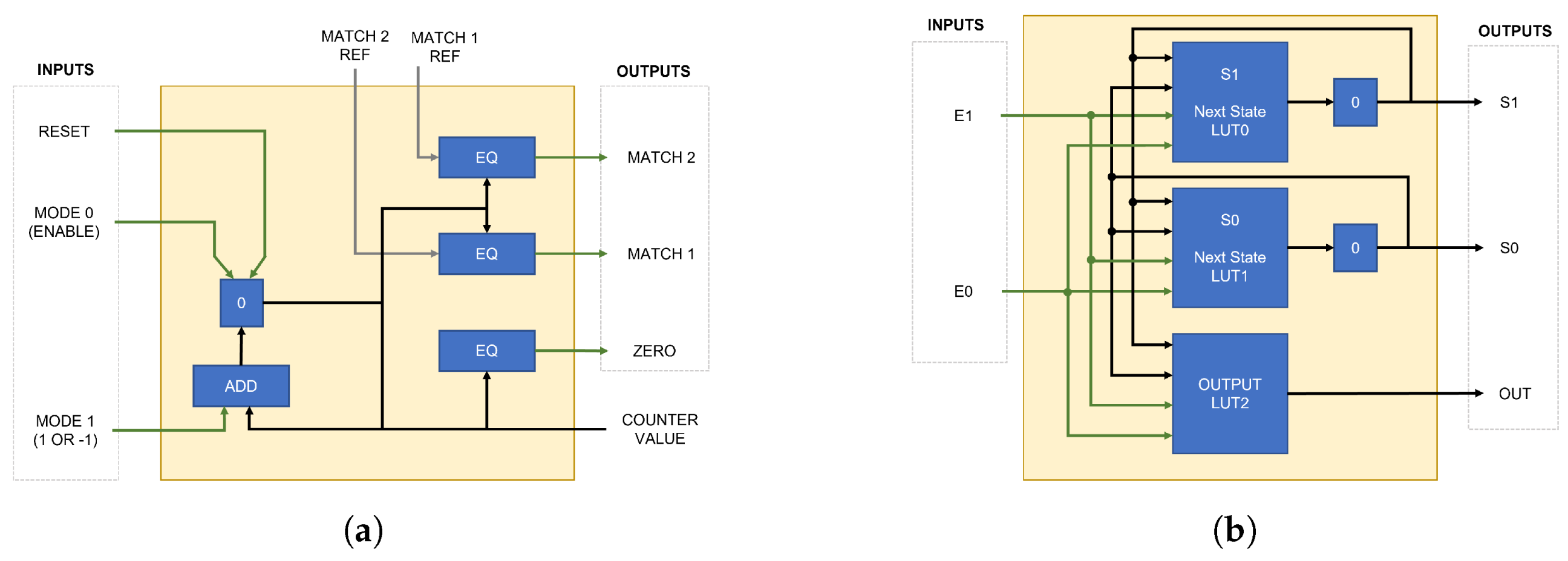
Figure 3 illustrates submodules residing within a CLB [21,25,26]. Among them, there are two key submodules for designing the EnDat interface master: the counter and FSM submodules. As shown in Figure 4a, a counter submodule has three inputs, four outputs, and two configuration parameters. The Reset input is responsible for resetting the counter value to zero, and the Mode 0 (M0) enables the counter while the Mode 1 (M1) determines the direction of counting, up or down. The MATCH1 and MATCH2 outputs generate pulse signals when the counter values match the MATCH1_REF and the MATCH2_REF, respectively. The Zero output generates a pulse when the counter value resets to zero. As shown in Figure 4b, an FSM submodule comprises two inputs, E0 and E1, two state variable bits, S0 and S1, and a single output, OUT. Inside the FSM, three look-up table (LUT) combinational logic blocks are provided to generate the next states and output.
In addition, in Figure 3, a LUT is composed of three or four inputs and one output, and the output can be designed as any form of combinational logic of inputs by controlling configuration registers; an HLC submodule provides the function to program instructions to process data between high-level controller (HLC) general-purpose registers (GPREG) and selected registers in CLB submodules.
The CLB is designed and implemented using the CLB tool, which is included in the TI’s code composer studio integrated development environment (CCS IDE), where the submodules of a CLB tile, such as LUTs, FSMs, and counters, are configured and programmed. Based on the design, the CLB tool generates C header and source files. The header file contains the submodule configuration parameters, and the source file contains the functions to load the submodule parameters into the submodule registers and program hardware logic, which are called and executed by the main function. For further details about CLB operation and programming, we refer the interested reader to [21,25,26].

3. Design and Implementation

In this section, we design and implement the EnDat interface master for the linear encoder slave complying with the EnDat protocol operation within the framework of the CLB peripheral. In order to facilitate the design process, we describe the operational sequence of the EnDat interface step by step as follows:
(i)
The interrupt service routine (ISR) of the enhanced pulse width modulator (EPWM) device sends an encoder data request signal to the EnDat interface master.
(ii)
According to the encoder data request, the EnDat interface master activates the master mode command enable (MCOM-EN), generates the EnDat clock (ENC-CLK), and sends the master mode command (MCOM) to the EnDat encoder slave through the data-out (DO) line of the RS-485 using the serial peripheral interface (SPI) device.
(iii)
In response to the ENC-CLK and MCOM from the master, the encoder slave returns the position data corresponding to the MCOM through the data-in (DI) line of the RS-485.
(iv)
As soon as the EnDat interface master receives the position data, it transfers the received data to the motor control program, and one cycle of the encoder data reading process is completed.
In the following subsections, we design each subsystem constituting the EnDat interface master to realize the above operation process steps. It is noticed that we consider the master mode command requesting only position data in the following design, but the design results can be used for any type of master mode commands.

3.1. Hardware Structure and Operation

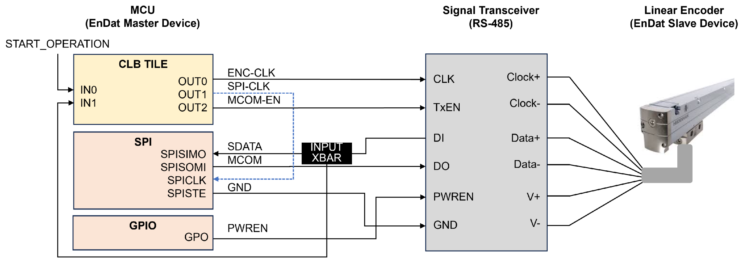
The hardware structure for the EnDat communication consists of an MCU, an EnDat encoder, and a signal transceiver, as illustrated in Figure 5. The MCU functions as an EnDat master device, while the linear encoder functions as an EnDat slave device. A half-duplex RS-485 device is essentially employed as a signal transceiver to facilitate communication between the master and encoder slave, such that the data transfer signal is robust to environmental noises and transmitted over a long distance.
The EnDat master is responsible for generating the necessary signals for the EnDat communication as well as receiving and processing position and additional operational data from the encoder slave. This function of the EnDat master is implemented using a CPU, a CLB, an SPI, a general-purpose input and output (GPIO) and a crossbar (XBAR). In Figure 5, the EnDat master needs to generate the ENC-CLK, SPI-CLK, and MCOM-EN signals and send an MCOM to the encoder slave as the SPI output through the DO input of the RS-485 device.
An XBAR is used to provide the CLB with the encoder data; the ENC-CLK is sent to the CLK input of the RS-485 device; and the SPI-CLK is transmitted from the CLB output directly to the SPICLK input of the SPI device. The ENC-CLK and MCOM signals are transformed into differential signals consisting of Clock+, Clock−, and Data+, Data−, respectively, in the RS-485 device. The MCOM signal is transmitted to the EnDat linear encoder slave in synchronization with the differential clock signal, and the MCOM-EN signal from CLB OUT2 is used to enable the signal transmission from the master to the slave in the half-duplex RS-485 transceiver.
After finishing sending the mode command via an MCOM signal, SPI-CLK is halted, and the MCOM-EN signal is set as low logic to activate the DI output of the transceiver and prepare to receive the encoder data. Then, the encoder slave sends the differential position data back to the transceiver, and the transceiver transforms the differential data signals to the single-ended data signal, which is sent to the SPI device as slave data (SDATA) while SPI-CLK is regenerated from the first rising edge of the SDATA signal. The signal timing diagram for the normal EnDat interface communication is illustrated in Figure 6.

3.2. Clock Generation

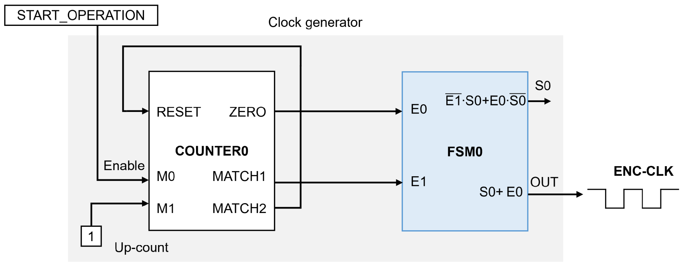
An FSM and a counter, whose basic operation principles are explained in Section 2.2, are key submodules employed in clock signal generation. As shown in Figure 7, the counter outputs, ZERO and MATCH1, are used as FSM inputs. By connecting the counter output MATCH2 to a counter input, RESET, a simple FSM configuration is designed, which is capable of generating a clock signal with a pulse width maintained between the MATCH1 and MATCH2 output pulses. The state diagram and state table are depicted in Figure 8 and Table 2 [27]. The next state equation and the output equation of the FSM are derived as
S 0 n + 1 = S 0 n · E 1 ¯ + S 0 ¯ n · E 0 = S 0 n · MATCH 1 ¯ + S 0 ¯ n · ZERO
OUT = S 0 n + E 0 = S 0 n + ZERO
where S 0 n and S 0 n + 1 denote the current and next state of the FSM; E0 and E1 denote the FSM inputs; and OUT denotes the FSM output. The timing diagram of this design is illustrated in Figure 9.
In this design, the resulting clock width and period are calculated using the equations (MATCH1_REF + 1) × SYSTEM_CLK_PERIOD and (MATCH2_REF + 1) × SYSTEM_CLK_PERIOD, respectively. In the following design of ENC-CLK and SPI-CLK, the system clock frequency is set as 200 MHz, and to synthesize 2 MHz clock signals, the MATCH1_REF and MATCH2_REF values are configured to 49 and 99, respectively.

3.3. Main FSM

The entire operation of the EnDat interface master is realized by the main FSM, which is implemented with the FSM2 submodule in the CLB, and the main FSM is denoted by the main FSM2 for clarity in the following discussion. The main FSM2 is designed with four states, IDLE, TRANMIT_DATA, WAIT, and RECEIVE_DATA; two inputs, E0 and E1; one output, OUT, as shown in Figure 10. The four states of the main FSM2 are represented with two binary bits, S0 and S1, and encoded as shown in Figure 10. In the following, the detailed operation at each state is described, and the main FSM2 is designed and implemented.
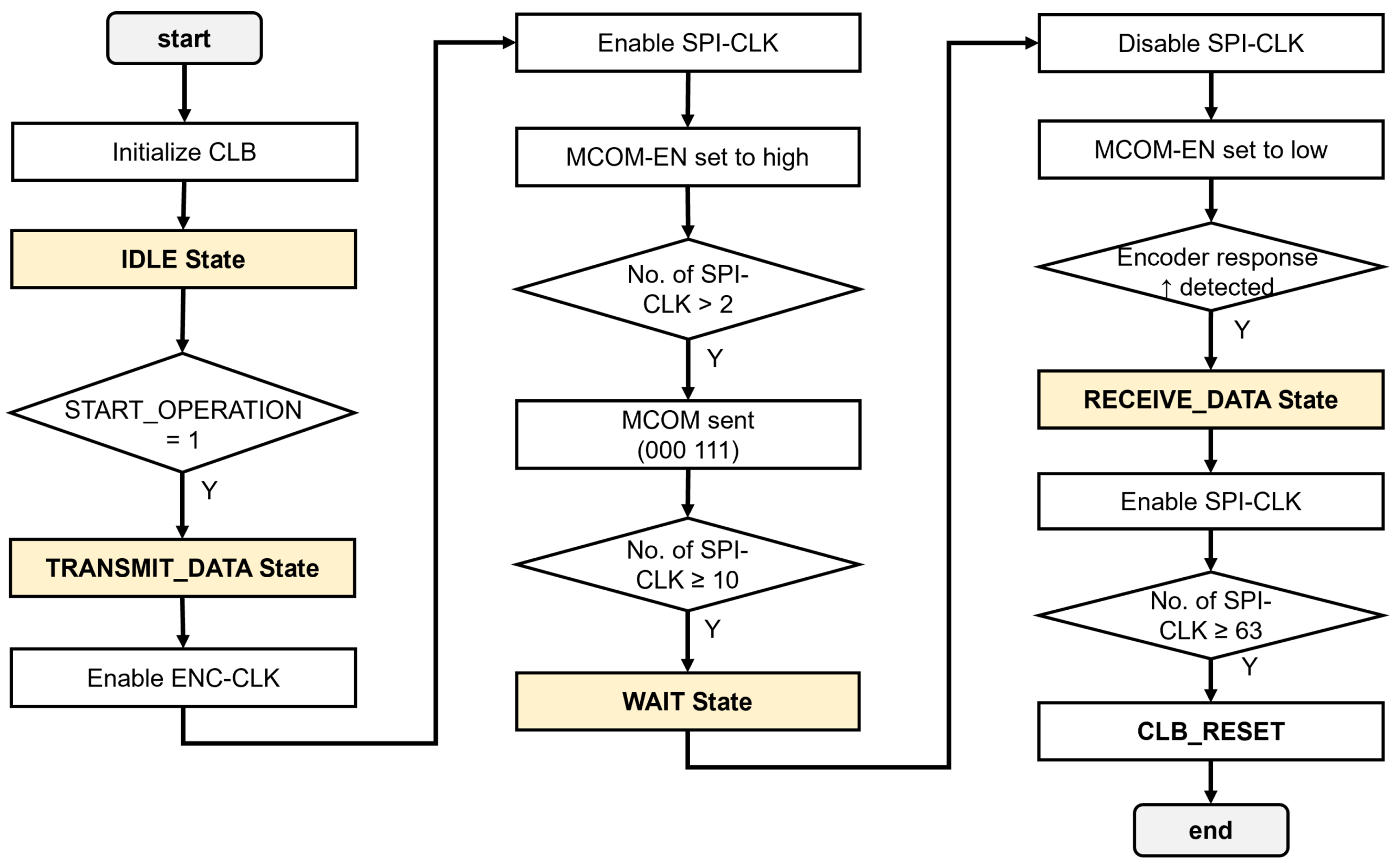
The IDLE state is the initial state and is transitioned to the TRANSMIT_DATA state by the START_OPERATION signal, which is synchronized with the motor control cycle and periodically activated by the EPWM ISR in the motor control program. Upon activation of the START_OPERATION, the state is transitioned from IDLE to TRANSMIT_DATA, and the ENC-CLK signal is generated by a dedicated clock generator in order to start the transmission cycle. The ENC-CLK generator is implemented using COUNTER0 and FSM0 in the CLB and enabled by the START_OPERATION signal that is connected to the M0 input of COUNTER0, as shown in Figure 11.
During the TRANMIT_DATA state, to send the mode command from the master to the slave, the SPI-CLK signal is generated, and the MCOM-EN signal is set to the active state. After the completion of the mode command transmission, the MCOM-EN signal is reset to the inactive state. As shown in Figure 12, the MCOM-EN signal is implemented with the OUTLUT2 submodule in the CLB and easily designed with the TRANSMIT_DATA state variable ( S 1 = 0 , S 0 = 1 ) as follows:
OUTLUT 2 . OUT = S 0 · S 1 ¯ .
The SPI-CLK is implemented with LUT0, COUNTER1, and FSM1 in the CLB, as shown in Figure 13, where it is noted that LUT0 is employed to generate the enable signal of the SPI-CLK. The SPI-CLK starts at the beginning of the TRANSMIT_DATA state; pauses during the WAIT state while awaiting the encoder’s response; and then restarts upon the reception of encoder data in the RECEIVE_DATA state. Thus, the main FSM2.S0 signal is used as an enable signal of the SPI-CLK because the main FSM2.S0 remains high logic during both the TRANSMIT_DATA and RECEIVE_DATA states. Hence, along with the START_OPERATION signal, the main FSM2.S0 is used for the LUT0 inputs as shown in Figure 13, and the output equation of LUT0 is designed as follows:
LUT 0 . OUT = START _ OPERATION · FSM 2 . S 0 .
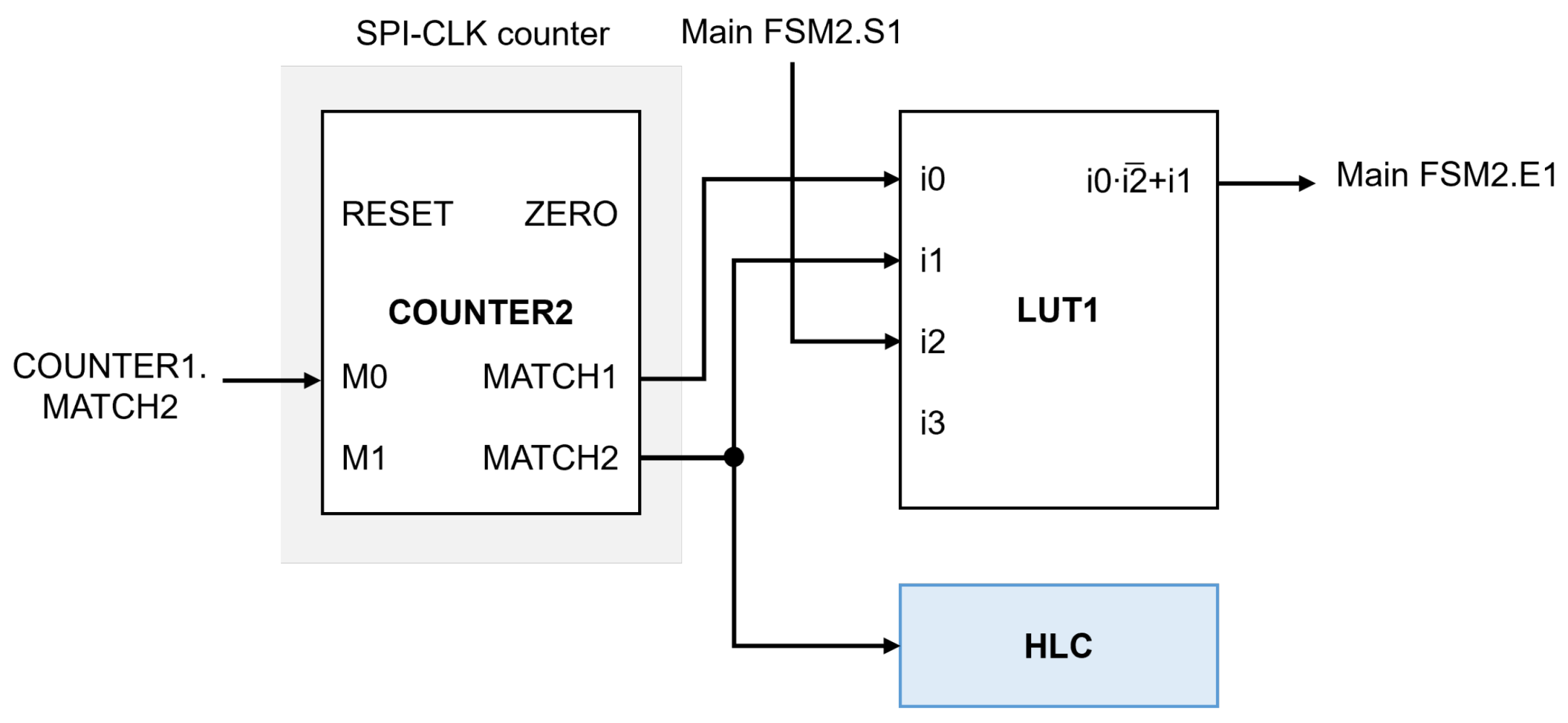
An SPI-CLK pulse counter is necessary because the TRANSMIT_DATA state is transitioned to the WAIT state after a specific number of SPI-CLK pulses occur. As shown in Figure 14, the SPI-CLK pulse counter is implemented with COUNTER2, LUT1, and HLC submodules. The COUNTER2 is responsible for counting the number of SPI-CLK pulses, and it is enabled by the COUNTER2.M0 input coming from COUNTER1.MATCH2, which is active only at the rising edge of the SPI-CLK. The COUNTER2.MATCH1 is changed to high logic when the counted number of SPI-CLK pulses reaches a specific value, which is the necessary number of SPI-CLK pulses in the TRANSMIT_DATA state and implemented by setting COUNTER2’s MATCH1_REF as ten. On the other hand, COUNTER2’s MATCH2_REF is set as 63, which is the necessary number of SPI-CLK pulses in the TRANSMIT_DATA and RECEIVE_DATA state, and indicates the completion of one communication cycle. That is, COUNTER2.MATCH2 is changed to high logic when the counted number of SPI-CLK pulses reaches 63 at the moment of one communication cycle completion.
The COUNTER2’s outputs and main FSM2.S1 are connected to LUT1 inputs, and LUT1.OUT is set to high logic when the SPI-CLK count reaches 10 and 63 in the TRANSMIT_DATA and RECEIVE_DATA state, respectively. This LUT1.OUT signal is connected to the main FSM2.E1 and activates the transitions from TRANSMIT_DATA to WAIT, and from RECEIVE_DATA to IDLE. To perform these state transitions, the LUT1.OUT is designed as follows:
LUT 1 . OUT = ( COUNTER 2 . MATCH 1 · FSM 2 . S 1 ¯ ) + COUNTER 2 . MATCH 2 .
Based on the above design, the overall structure and the flowchart of the CLB design for EnDat interface implementation are illustrated in Figure 15 and Figure 16, respectively, and the state table of the main FSM2 is created in Table 3. Applying the logic reduction technique based on the Karnaugh maps, the final logic equations for state transition are designed as follows:
S 0 n + 1 = ( S 0 ¯ n · S 1 n · E 0 ) + ( S 0 n · E 1 ¯ ) + ( S 0 ¯ n · S 1 ¯ n )
S 1 n + 1 = ( S 0 ¯ n · S 1 n ) + ( S 0 n · S 1 n · E 1 ¯ ) + ( S 0 n · S 1 ¯ n · E 1 ) .

4. Experiments and Results

4.1. Feed Drive Control System

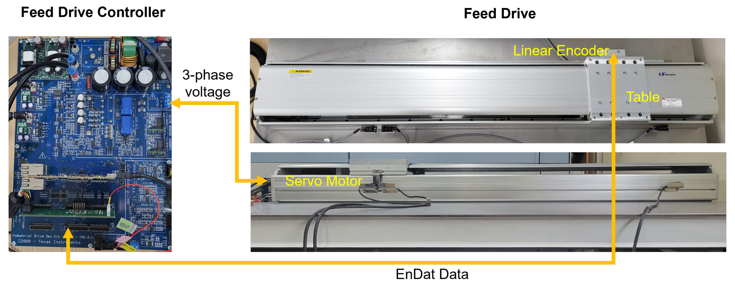
To verify the normal operation and performance of the developed EnDat interface and demonstrate its practical usefulness, we build a one-axis feed drive system consisting of TI’s TMS320F28388D DSP control card, TI’s DesignDRIVE Development Kit (IDDK), and Heidenhain’s LC 416 EnDat linear encoder, as shown in Figure 17. A permanent magnet synchronous motor (PMSM) is installed to rotate the shaft and activate the linear movement of the nut and the table in the feed drive system. The EnDat linear encoder is installed to measure the table position and speed. The specifications of the EnDat linear encoder, LC 416, from Heidenhain, are listed in Table 4.
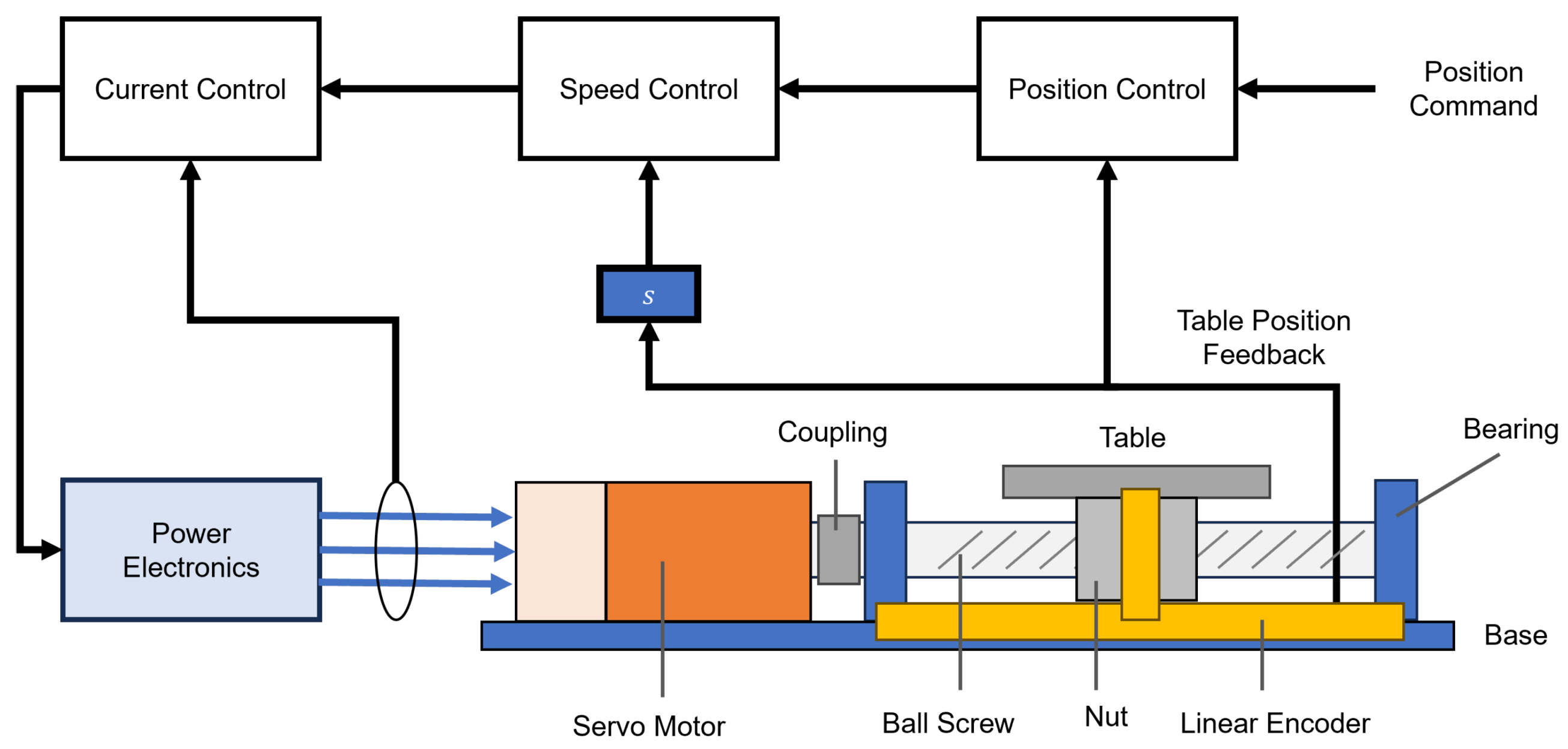
As the motor control scheme for the feed drive system, we employ the widely used field-oriented control (FOC) technique under the maximum torque per ampere strategy. This approach is implemented with one proportional (P) controller and two proportional and integral (PI) controllers, which are responsible for table position, speed, and current control, respectively. The overall structure of the feed drive control scheme is depicted in Figure 18, where we intentionally omit the direct-quadrature-zero (DQZ) transformation and space vector PWM (SVPWM) functions to facilitate the conceptual understanding by avoiding the complex representation.
The control cycles for the table position and speed are set as 1 kHz and 2 kHz, respectively, and the current control cycle is set as 16 kHz, which is a common setup for the precise position control in machine tool applications. Accordingly, the current control is performed in EPWM ISR at the 16 kHz frequency, which is calculated as 62.5 μ s in cycle time. In the experiments, during each current control cycle, the motor control algorithm generates the START_OPERATION signal to obtain the table position feedback from the EnDat linear encoder. To ensure that the EnDat communication cycle remains within the current control cycle, we set the EnDat clock frequency as 2 MHz.

4.2. EnDat Interface Verification

We verify the normal operation of the developed EnDat interface by monitoring and measuring the ENC-CLK, MCOM-EN, MCOM, and SDATA signals while running the table speed and position control program with 2 MHz ENC-CLK. In Figure 19, the measured master signals are shown for one cycle of the EnDat communication with the EnDat clock frequency of 2 MHz. As shown in Figure 19, the normal operation of the EnDat interface master is verified by observing that the ENC-CLK occurs continuously throughout the communication cycle; the MCOM-EN signal remains at a high logic until all mode command bits (000 111) are transmitted, after which it is transitioned to a low logic; and the SDATA signal including a 36-bit position value and 5-bit CRC value is received from the encoder. Moreover, the entire cycle time is measured with about 35 μ s, which is definitely less than the current control cycle, 62.5 μ s.

4.3. Control Performance of Feed Drive System

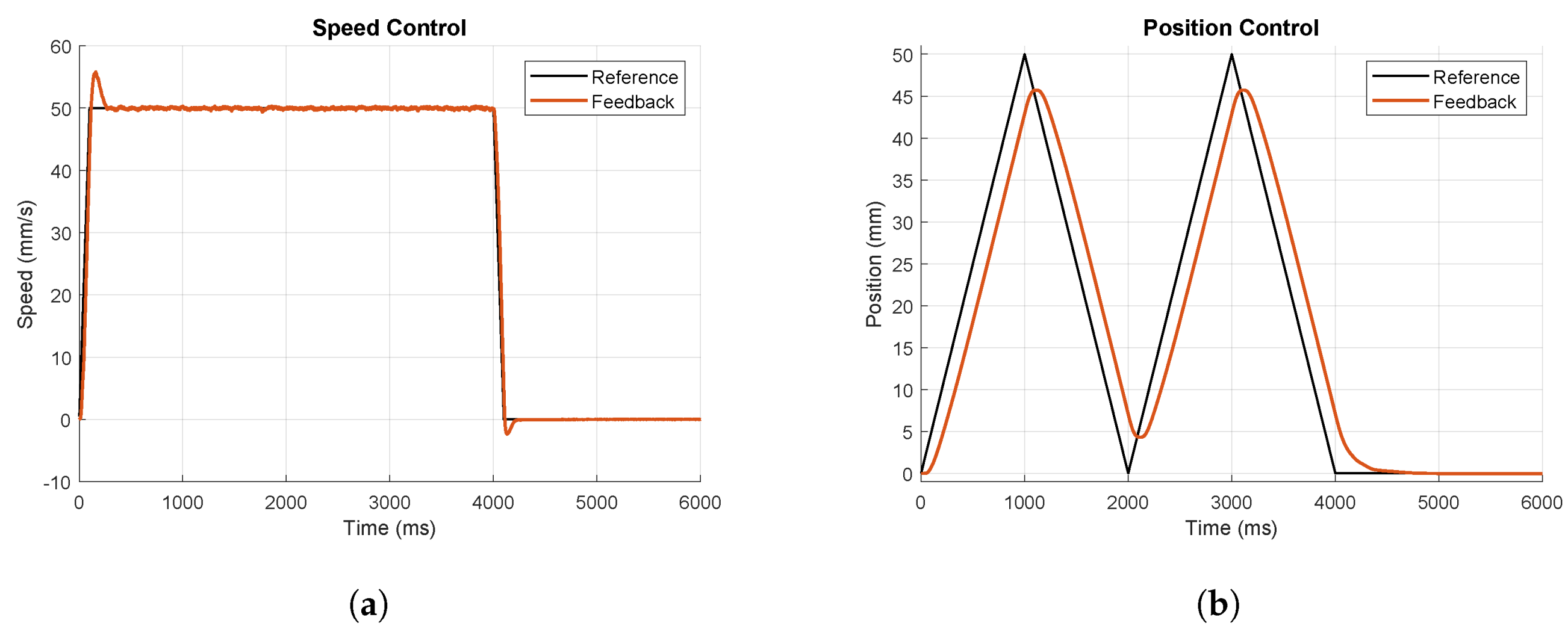
To validate the practical usefulness of the developed EnDat interface master, we conduct experiments for table speed and position control with the position feedback from the linear encoder. In the speed control experiment, the reference target speed is set as 50 mm/s, while the reference target position is formed in a two-triangular shape in the position control experiment. The experimental results are shown in Figure 20, which demonstrates that the table speed and position are normally controlled such that they converge to the reference target values without significant errors. This observation verifies the normal operation of the developed EnDat interface master and the reliability of the feedback position data from the linear encoder. Therefore, it is confirmed that the developed EnDat interface master is fully implemented and suitable for real applications.
On the other hand, the speed response in Figure 20a shows an overshoot, which is unavoidable due to the effect of a zero generated by the PI speed controller. This overshoot can be removed by employing an IP or PI-IP controller, but the performance of response speed is sacrificed as a trade-off; that is, the rise time of the speed response is increased. In addition, it is a common technique in the feed drive control system that the P position controller is designed so that the overshoot does not occur in the table position response. Therefore, it is natural that the table position response shows a limited bandwidth and slow response, as shown in Figure 20b. This limited bandwidth and slow response can be improved by increasing the proportional gain, but a gain that is too high may cause the system to become unstable [28].

5. Conclusions

We have developed a CLB-based EnDat interface master for feed drive control systems demanding high-precision and high-frequency processing. By analyzing the EnDat interface protocol, we derive the truth and state tables to design the main FSM and other logic combinations for EnDat master implementation. By programming the designed logic using the CLB submodules, the operation process of the EnDat interface master is successfully realized with the generation of ENC-CLK, MCOM-EN, SPI-CLK, and MCOM signals. This development offers substantial cost-efficiency as it eliminates the need for external logic programming devices like FPGAs or CPLDs, thereby reducing the number of IC components, PCB dimensions, artwork intricacy, and power consumption, as summarized in Table 5. Moreover, this implementation method is flexible enough to allow for immediate application in system development employing CLB-integrated MCUs and EnDat encoders, and it presents opportunities for enhancing encoder data processing efficiency in various applications, including smart factories.
To verify the performance and practical usefulness of the developed master, a series of experiments were conducted using a one-axis feed drive system. These experiments confirmed that the EnDat clock frequency of 2 MHz could be achieved without the need for propagation delay compensation. The practical usefulness of our approach was further demonstrated through table speed and position control performance that meets real-world application requirements.
In future research, we suggest enhancing the clock frequency to reach 16 MHz, which may be achieved by improving transceiver devices with higher speeds, applying the propagation delay compensation, and tuning the SPI interface program.

Author Contributions

Conceptualization and methodology, K.K.; software, K.K.; validation, D.M.T.; formal analysis, K.K.; investigation, J.-Y.C.; resources, K.K.; data curation, K.K. and D.M.T.; writing—original draft preparation, K.K.; writing—review and editing, K.K., D.M.T. and J.-Y.C.; visualization, K.K.; supervision, J.-Y.C.; project administration, J.-Y.C.; K.K. and D.M.T. are equal contributors to this work and designated as co-first authors. All authors have read and agreed to the published version of the manuscript.

Funding

This work was supported by the Korea Evaluation Institute of Industrial Technology (KEIT) and the Ministry of Trade, Industry & Energy (MOTIE) of the Republic of Korea (No. 20012815).

Data Availability Statement

The data presented in this study are available on request from the corresponding author.

Conflicts of Interest

The authors declare no conflict of interest.

References

  1. Bosetti, P.; Bruschi, S. Enhancing positioning accuracy of CNC machine tools by means of direct meas-urement of deformation. Int. J. Adv. Manuf. Technol. 2012, 58, 651–662. [Google Scholar] [CrossRef]
  2. Kwon, Y.; Tseng, T.L.; Ertekin, Y. Characterization of closed-loop measurement accuracy in precision CNC milling. Robot. Comput.-Integr. Manuf. 2006, 22, 288–296. [Google Scholar] [CrossRef]
  3. Zha, C.L.; Wang, C.N.; Chen, S.J. Design of NC Machine Tools Self-Compensation System Based on FPGA. Appl. Mech. Mater. 2013, 278, 1442–1446. [Google Scholar] [CrossRef]
  4. Hubeatir, K.A.; Al-Kafaji, M.M.; Omran, H.J. A review: Effect of different laser types on material engraving process. J. Mater. Sci. 2018, 6, 210–217. [Google Scholar]
  5. Kim, J.; Guo, A.; Yeh, T.; Hudson, S.E.; Mankoff, J. Understanding uncertainty in measurement and accommodating its impact in 3D modeling and printing. In Proceedings of the 2017 Conference on Designing Interactive Systems, Edinburg, UK, 10–14 June 2017; pp. 1067–1078. [Google Scholar]
  6. Zhao, J.; Wang, H.; Zhao, J.; Pan, Z.; Yan, R. Precise positioning of linear motor mover directly from the phase difference analysis. IEEE/ASME Trans. Mechatron. 2020, 25, 1566–1577. [Google Scholar] [CrossRef]
  7. Sato, K. High-precision and high-speed positioning of 100 G linear synchronous motor. Precis. Eng. 2015, 39, 31–37. [Google Scholar] [CrossRef]
  8. Shi, Y.; Zhou, Q.; Li, X.; Ni, K.; Wang, X. Design and testing of a linear encoder capable of measuring ab-solute distance. Sens. Actuators A Phys. 2020, 308, 111935. [Google Scholar] [CrossRef]
  9. Gao, W.; Kim, S.W.; Bosse, H.; Haitjema, H.; Chen, Y.L.; Lu, X.D.; Knapp, W.; Weckenmann, A.; Estler, W.T.; Kunzmann, H. Measurement technologies for precision positioning. CIRP Ann. 2015, 64, 773–796. [Google Scholar] [CrossRef]
  10. Shriram, S.; Barkur, R.; Joshua, P.; Shanthibhushan, B. Work-in-Progress: FPGA Implementation of Synchronous Serial Interface for Hardware in Loop Simulation. In Proceedings of the 2017 IEEE Real-Time and Embedded Technology and Applications Symposium (RTAS), Pittsburgh, PA, USA, 18–21 April 2017; pp. 133–136. [Google Scholar]
  11. Wilkening, T.; Krah, J.O.; Goergen, H. Safety-Related Interfaces for Position Encoders-a Survey. In Proceedings of the PCIM Europe 2019, International Exhibition and Conference for Power Electronics, Intelligent Motion, Renewable Energy and Energy Management, Nuremberg, Germany, 7–9 May 2019. [Google Scholar]
  12. Ye, W.; Cai, C.; Wang, B.; Yang, P. Decoding of BISS-C Protocol Based on FPGA. In Proceedings of the 2019 Chinese Automation Congress (CAC), Hangzhou, China, 22–24 November 2019; pp. 288–291. [Google Scholar]
  13. Xiang, Q.; Li, L.; Zhu, L.; Chen, H. A Realization Method of Cooperative Robot Servo Based on BISS-C Encoder. In Proceedings of the 2020 Chinese Automation Congress (CAC), Shanghai, China, 6–8 November 2020; pp. 6444–6447. [Google Scholar]
  14. Texas Instruments. C2000 Position Manager EnDat22 Library Module, User’s Guide; Texas Instruments: Dallas, TX, USA, 2015. [Google Scholar]
  15. Texas Instruments. Universal Digital Interface to Absolute Position Encoders; Texas Instruments: Dallas, TX, USA, 2015. [Google Scholar]
  16. Heidenhain. EnDat 2.2-Bidirectional Interface for Position Encoders; Heidenhain: Traunreut, Germany, 2011. [Google Scholar]
  17. Liu, J.; Chen, S.; Zhang, G.; Shi, L. The development of a novel servo motor controller based on EtherCAT and FPGA. In Proceedings of the 2016 Chinese Control and Decision Conference (CCDC), Yinchuan, China, 28–30 May 2016; pp. 3174–3179. [Google Scholar]
  18. Zhao, B.; Zhang, H.; Zhang, T. Configurable and Modular Development of Multi-Channel Motion Control Encoder Feedback System. In Proceedings of the 2018 5th International Conference on Information Science and Control En-gineering (ICISCE), Zhengzhou, China, 20–22 July 2018; pp. 665–669. [Google Scholar]
  19. Hino, R.; Le Caer, T.; Le Mentec, F.; Fajardo, P.; Janvier, N. A position encoder processing unit. Power 2017, 5, 6x. [Google Scholar]
  20. Schmidt, T.; Krah, J.O.; Holtz, J. High-performance control architecture for automation drives based on a low-cost microcontroller in combination with a low-cost FPGA. In Proceedings of the PCIM Europe Digital Days 2021, International Exhibition and Conference for Power Electronics, Intelligent Motion, Renewable Energy and Energy Management, Online, 3–7 May 2021; pp. 1–8. [Google Scholar]
  21. Galicki, P. Application Report: How to Migrate Custom Logic from an FPGA/CPLD to C2000 Microcon-Trollers; Texas Instruments: Dallas, TX, USA, 2020. [Google Scholar]
  22. Peterka, J.; Nikitin, Y.R.; Bozek, P. Diagnostics of automated technological devices. MM Sci. J. 2020, 4027–4034. [Google Scholar] [CrossRef]
  23. Šegota, S.B.; Andeli´c, N.; Mrzljak, V.; Lorencin, I.; Kuric, I.; Car, Z. Utilization of multilayer perceptron for determining the inverse kinematics of an industrial robotic manipulator. Int. J. Adv. Robot. Syst. 2021, 18, 1729881420925283. [Google Scholar] [CrossRef]
  24. EnDat Interface from HEIDENHAIN: Proven Interface Technology Continuously Further Developed. Available online: https://endat.heidenhain.com/ (accessed on 29 November 2023).
  25. Texas Instruments. Designing with the C2000 Configurable Logic Block (CLB); Texas Instruments: Dallas, TX, USA, 2019. [Google Scholar]
  26. Tran, D.M.; Kim, K.; Choi, J.Y. CLB-Based Development of BiSS-C Interface Master for Motor Encoders. Electronics 2023, 12, 886. [Google Scholar] [CrossRef]
  27. Marcovitz, A.B. Introduction to Logic Design; McGraw-Hill Higher Education: New York, NY, USA, 2010. [Google Scholar]
  28. Nam, K.H. AC Motor Control and Electrical Vehicle Applications; CRC Press: Boca Raton, FL, USA, 2018. [Google Scholar]
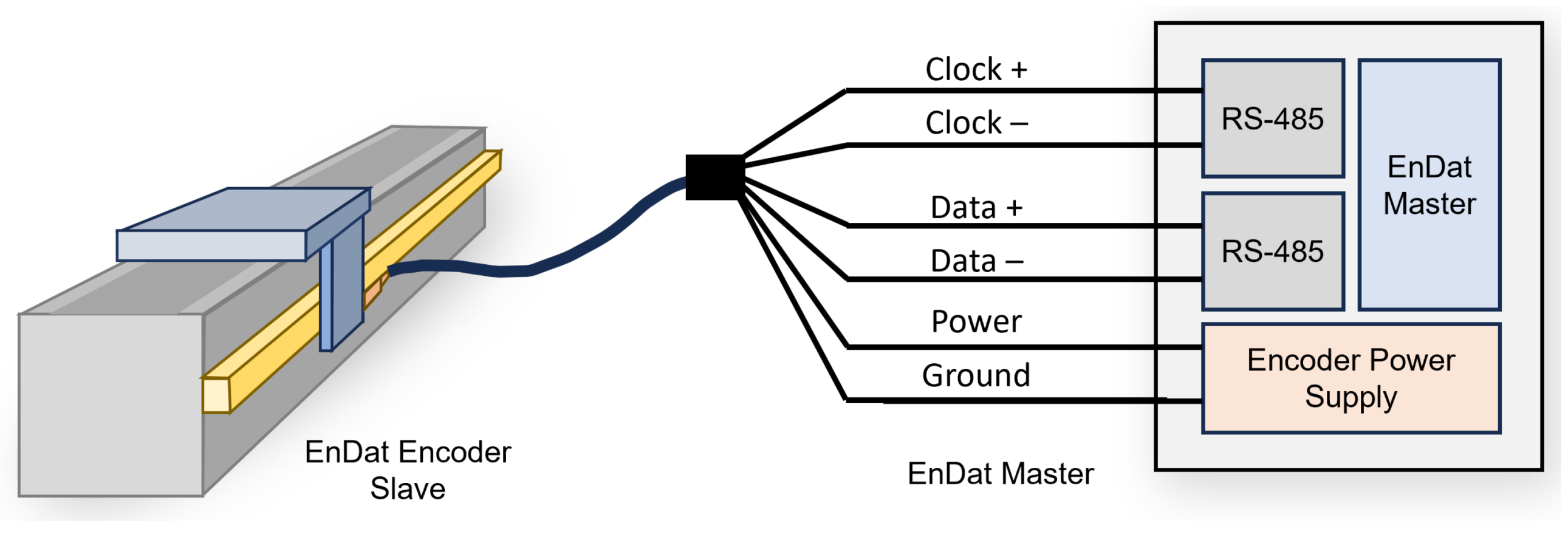
Figure 1. Structure of EnDat point-to-point connection between master and slave.
Electronics 13 01101 g001
Figure 2. EnDat frame in a point-to-point configuration.
Electronics 13 01101 g002
Figure 3. CLB tile structure.
Electronics 13 01101 g003
Figure 4. Submodule structures. (a) Counter. (b) FSM.
Electronics 13 01101 g004
Figure 5. Hardware structure of EnDat interface implementation.
Electronics 13 01101 g005
Figure 6. Signal timing for one cycle of EnDat communication.
Electronics 13 01101 g006
Figure 7. Clock generation structure consisting of counter and FSM.
Electronics 13 01101 g007
Figure 8. State diagram of clock generation FSM.
Electronics 13 01101 g008
Figure 9. Signal timing of counter and FSM for clock generation.
Electronics 13 01101 g009
Figure 10. State diagram for EnDat interface master operation.
Electronics 13 01101 g010
Figure 11. CLB submodule design to generate EnDat ENC-CLK signals.
Electronics 13 01101 g011
Figure 12. CLB submodule design to generate EnDat MCOM-EN signals.
Electronics 13 01101 g012
Figure 13. CLB submodule design to generate SPI-CLK signals.
Electronics 13 01101 g013
Figure 14. CLB submodule design to count SPI-CLK and trigger HLC interrupt.
Electronics 13 01101 g014
Figure 15. Overall structure of CLB design for EnDat interface master.
Electronics 13 01101 g015
Figure 16. Flowchart of EnDat interface implementation.
Electronics 13 01101 g016
Figure 17. Experimental environment.
Electronics 13 01101 g017
Figure 18. Structure of feed drive control system.
Electronics 13 01101 g018
Figure 19. Measured signals in EnDat interface communication: EnDat clock (ENC-CLK, yellow), master command enable (MCOM-EN, magenta), master mode command (MCOM, blue), and slave data (SDATA, green).
Electronics 13 01101 g019
Figure 20. Feed drive control results using EnDat linear encoder. (a) Speed reference and response. (b) Position reference and response.
Electronics 13 01101 g020
Table 1. Comparison of encoder serial communication protocols.
ProtocolSSIHiperFace DSLBiSS-CEnDat
OwnershipSickSickiC-HausHeidenhain
Serial Bit Rate80 kHz to 2 MHz9.375 Mbps80 kbps to 10 Mbps100 kbps to 16 Mbps
Max Cable LengthVendor specific100 m100 m100 m
Propagation Delay CompensationNot supportedSupportedSupportedSupported
PHYRS-422RS-485RS-422RS-485
Power SupplyVendor specific7 V to 12 V5 V to 30 V3.6 V to 14 V
Table 2. State table of clock generation FSM.
Current StateNext StateOUT
State S 0 n E1 E0 S 0 n + 1
Low00000
00111
01000
01111
High10011
10111
11001
11101
Table 3. State table of main FSM.
Current StateNext State
Status S 1 n S 0 n E 1 n E 0 n S 1 n + 1 S 0 n + 1
IDLE000001
000101
001001
001101
TRANSMIT_DATA010001
010101
011010
011110
WAIT100010
100111
101010
101111
RECEIVE_DATA110011
110111
111000
111100
Table 4. Specifications of linear encoder, Heidenhain LC 416.
ParameterValue
ManufacturerHeidenhain
Model NameLC 416
Encoder TypeLinear
Accuracy Grade5 μ m
Measuring Length920 mm
Compatible InterfaceEnDat 2.1, EnDat 2.2
Measuring Step0.010 μ m
Table 5. Characteristic comparisons between external device-based and proposed implementations.
Implementation ApproachNumber of ComponentsPCB Size and ComplexityPower ConsumptionProduction and Maintenance Cost
Using MCU and external programmable deviceIncreasedIncreasedIncreasedIncreased
Using only MCU (Using integrated CLB and SPI)ReducedReducedReducedReduced
Disclaimer/Publisher’s Note: The statements, opinions and data contained in all publications are solely those of the individual author(s) and contributor(s) and not of MDPI and/or the editor(s). MDPI and/or the editor(s) disclaim responsibility for any injury to people or property resulting from any ideas, methods, instructions or products referred to in the content.