
Control of Threshold Voltage in ZnO/Al2O3 Thin-Film Transistors through Al2O3 Growth Temperature

Department of Electrical and Electronics Engineering, Pusan National University, Busan 46241, Republic of Korea
*
Author to whom correspondence should be addressed.
Electronics 2024, 13(8), 1544; https://doi.org/10.3390/electronics13081544
Submission received: 8 February 2024
/
Revised: 8 April 2024
/
Accepted: 16 April 2024
/
Published: 18 April 2024
(This article belongs to the Section Semiconductor Devices)
Abstract
:Ultra-thin ZnO thin-film transistors with a channel thickness of <10 nm have disadvantages of a high threshold voltage and a low carrier mobility due to a low carrier concentration. Although these issues can be addressed by utilizing the strong reducing power of tri-methyl-aluminum, a method is required to control parameters such as the threshold voltage. Therefore, we fabricated a ZnO/Al2O3 thin-film transistor with a thickness of 6 nm and adjusted the threshold voltage and carrier mobility through the modulation of carrier generation by varying the growth temperature of Al2O3. As the growth temperature of Al2O3 increased, oxygen vacancies generated at the hetero–oxide interface increased, supplying a free carrier into the channel and causing the threshold voltage to shift in the negative direction. The optimized device, a ZnO/Al2O3 thin-film transistor with a growth temperature of 140 °C, exhibited a μsat of 12.26 cm2/V∙s, Vth of 8.16 V, SS of 0.65 V/decade, and ION/OFF of 3.98 × 10⁶. X-ray photoelectron spectroscopy was performed to analyze the properties of ZnO/Al2O3 thin films.
1. Introduction
Over the last few years, amorphous oxide thin-film transistors (TFTs) are extensively studied due to their numerous advantages such as transparency in visible light, uniformity, high electron mobility and low processing temperature suitable for flexible substrates [1,2,3]. Because of these advantages, amorphous oxide TFTs are expected to be utilized in the emerging next generation displays, such as Augmented Reality (AR) and Virtual Reality (VR) displays. These next generation displays demand resolutions in the order of several thousand pixels per inch (ppi), far surpassing the 100–500 ppi resolution found in traditional devices like smartphones and TVs. Therefore, to meet these requirements, scaling of TFTs is essential. However, in oxide semiconductors, the total number of free electrons is proportional to the thickness of the channel. Therefore, during scaling, as the channel becomes thinner, the number of free electrons within the channel decreases, resulting in TFTs having high threshold voltages and low mobility. Due to these issues, the amorphous oxide semiconductor material ZnO, commonly employed as the channel layer material for TFTs, faces challenges in being utilized at thicknesses below 10 nm [4,5,6,7].
To supply free electrons in an ultra-thin ZnO channel, a high reductive agent such as a tri-methyl-aluminum (TMA) precursor can be utilized. The TMA reduces the bottom layer and forms oxygen vacancies which are a major source of free electrons in oxide TFT on the bottom layer [8,9,10,11,12,13]. The oxygen vacancies, generated by TMA, are concentrated at the interface between ZnO and Al2O3 and act as electron donors, facilitating the provision of free electrons even in thin ZnO channel layers with a thickness of less than 10 nm.
The threshold voltage (Vth) adjustment is crucial as it influences the power consumption of TFT devices. Adjusting Vth can be realized by either altering the channel thickness or controlling the oxygen vacancy concentration within the channel [14,15,16,17]. In the case of the ZnO/Al2O3 channel, which are supplied with free electrons through the reducing power of TMA, Vth control was achieved by adjusting the thickness of either the upper layer (Al2O3) or the bottom layer (ZnO). However, adjusting the thickness of the upper layer or the bottom layer may conflict with scaling the device. Therefore, a new approach to adjust Vth is required.
Therefore, in this study, we aimed to adjust the Vth in ultra-thin ZnO/Al2O3 TFTs through the growth temperature of Al2O3. Specifically, we adjusted the oxygen vacancies through the growth temperature of Al2O3 as a method for controlling the threshold voltage applicable to ultra-thin ZnO/Al2O3 TFTs. Through X-ray photoelectron spectroscopy (XPS) analysis, it was confirmed that an increase in the growth temperature of Al2O3 from 110 °C to 150 °C resulted in a higher concentration of oxygen vacancies generated at the channel due to the reduction power of TMA. Consequently, the increase in the growth temperature of Al2O3 led to a generation of more free carriers in ZnO/ Al2O3 TFT, resulting in a negative shift in Vth.
2. Materials and Methods
Inverted-staggered type ZnO and ZnO/Al2O3 TFTs were fabricated on Si/SiO2 wafers used as the substrate. Heavily doped p-type Si is acting as the gate electrode, and a 100nm thick thermally grown SiO2 is acting as a gate dielectric. The ZnO and Al2O3 thin films were deposited using diethylzinc (DEZ), TMA, and H2O as a Zn precursor, an Al precursor, and an oxidant, respectively. In ZnO deposition, one cycle of ALD consisted of exposure to DEZ (0.3 s), a 20 s purge, exposure to H2O (0.3 s), and a 20 s purge. In Al2O3 deposition, one cycle of ALD consisted of exposure to TMA (0.3s), a 20 s purge, exposure to H2O (0.3 s), and a 20 s purge. N2 gas flowing at a rate of 60sccm was used to deliver the precursors into the reaction chamber. The working pressure in the chamber was 200 mTorr. The deposition rates of ZnO and Al2O3 were 2 Å/cycle and 1 Å/cycle, respectively.
First, in order to confirm the effect of the Al2O3 layer thickness, the ZnO films with Al2O3 layer thicknesses of 0 nm and the ZnO/Al2O3 films with Al2O3 layer thicknesses of 1 nm and 2 nm were deposited as the channel layer of TFTs. The total thickness of the ZnO and ZnO/Al2O3 channel layers was fixed at 6 nm, and the growth temperature of the film was 110 °C. To investigate the effect of Al2O3 growth temperature, ZnO/Al2O3 TFTs with a 1 nm thick Al2O3 layer were fabricated. The total thickness of the ZnO/Al2O3 channel layers was fixed at 6nm, and the growth temperature of ZnO was fixed at 110 °C, and the growth temperature of Al2O3 was increased from 110 °C to 150 °C in increments of 10 °C. In addition, to investigate the influence according to the growth temperature of ZnO, growth temperature of Al2O3 was fixed at 140 °C, and the growth temperature of ZnO was increased to 110 °C, 130 °C, 140 °C, and 150 °C. An additional annealing process was not performed to prevent Al diffusion. Next, 100 nm thick Al was deposited using a shadow mask by a thermal evaporator to serve as the source/drain (S/D) electrodes. The fabricated TFTs had a channel width (W) and length (L) of 1000 μm and 100 μm, respectively. Figure 1 shows the cross-sectional schematic diagram of the fabricated inverted-staggered type (a) ZnO and (b) ZnO/Al2O3 TFTs.
The oxygen binding states in the ZnO/Al2O3 layers were analyzed by XPS in order to confirm the effect according to the growth temperature of Al2O3. The electrical characteristics of the fabricated TFTs were measured using an EL423 semiconductor parameter analyzer from Elecs Co.
3. Results and Discussion
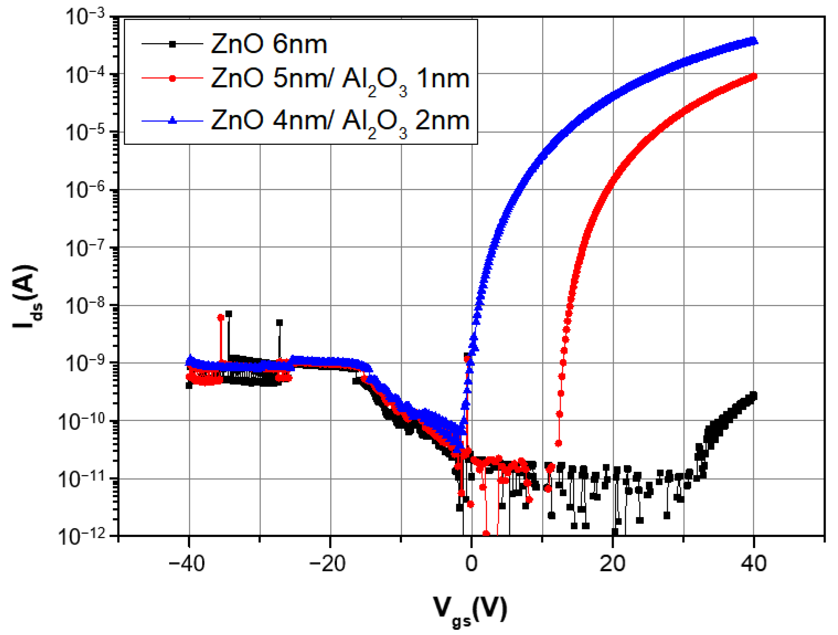
Figure 2 presents the transfer characteristic curves of ZnO/Al2O3 TFTs according to the thickness of Al2O3. In the case of a ZnO/Al2O3 TFT with an Al2O3 thickness of 0nm (ZnO TFT), there is an insufficiency of free electrons in the channel. Consequently, ZnO TFT with a channel thickness of 6 nm exhibits a significantly high Vth exceeding 40 V and a low saturation mobility of 0.0088 cm2/V∙s. However, in the cases of ZnO (5 nm)/Al2O3 (1 nm) TFT and ZnO (4 nm)/Al2O3 (2 nm) TFT, the Vth shifted towards the negative compared to the ZnO TFT, and there was an improvement in saturation mobility and an increase in the on current. This indicates that when the Al2O3 is deposited onto the ZnO layer, oxygen vacancies are generated in the ZnO layer due to the reducing power of TMA, supplying free electrons into the channel. Furthermore, as the Al2O3 thickness increased from 1nm to 2 nm, the Vth shifted in the negative direction from 22.24 V to 9.60 V, and the saturation mobility increased from 1.54 cm2/V∙s to 2.82 cm2/V∙s. The negative shift in Vth and improvement in saturation mobility with increasing thickness of Al2O3 is attributed to the increased generation of free electrons in the ZnO layer. It aligns with the results of other studies that suggest an increase due to carrier confinement through the Al2O3 barrier [9,18,19].
The electrical parameters, such as saturation mobility (μsat), Vth, SS, and on–off current ratio (ION/OFF) of ZnO/Al2O3 TFTs according to the thickness of Al2O3, are presented in Table 1.
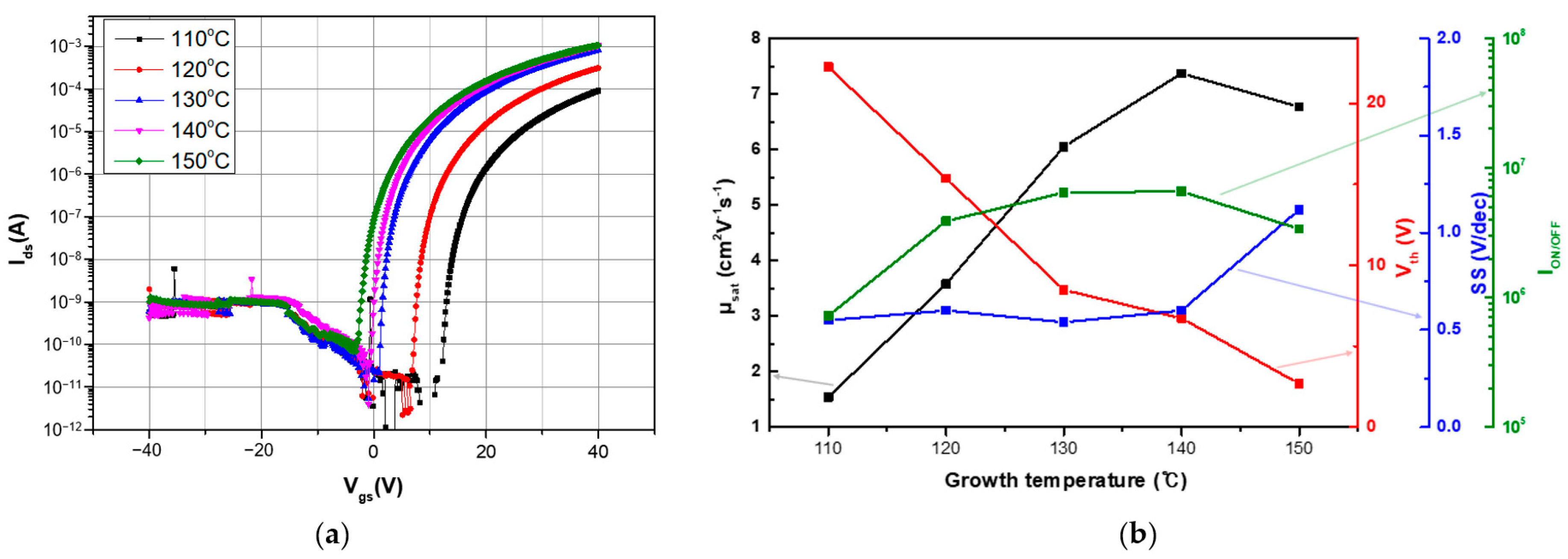
Figure 3a shows the transfer characteristic curves of ZnO/Al2O3 TFTs with Al2O3 growth temperatures of 110 °C, 120 °C, 130 °C, 140 °C, and 150 °C. The Vth of ZnO/Al2O3 TFT decreases from 22.24 V to 2.68 V as the growth temperature of Al2O3 increases from 110 °C to 150 °C, accompanied by an increase in the on current. Typically, as the carrier concentration in the channel increases, the Vth shifts in the negative direction, and the on current increases. Therefore, it can be inferred that as the growth temperature of Al2O3 increases from 110 °C to 150 °C, the carrier density in the channel increases. Since the growth temperature of ZnO was fixed at 110 °C, the increase in carrier concentration with the increased growth temperature of Al2O3 is attributed to the oxygen vacancies generated by the reducing power of TMA. Furthermore, as the growth temperature of Al2O3 increases, the free electrons in the channel increase due to the reducing power of TMA, resulting in an increase in the saturation mobility from 1.54 cm2/V∙s to 7.37 cm2/V∙s.
As the growth temperature of Al2O3 increases, the Vth shifts decrease. When the growth temperature of Al2O3 increases from 110 °C to 120 °C, the threshold voltage shifts from 22.24 V to 15.36 V. However, when the growth temperature of Al2O3 increases from 130 °C to 140 °C, the threshold voltage shifts from 8.48 V to 6.72 V. This indicates that as the growth temperature of Al2O3 increases, the generation of oxygen vacancies and free electrons in the channel gradually decreases due to the reducing power of TMA. Moreover, as the growth temperature of Al2O3 increases, both the on current and off current increase. Therefore, except for 110 °C and 120 °C where there is a significant difference in the increase in the on current compared to the increase in the off current, the on–off ratio maintains a constant value.
Another notable feature is the degradation of SS when the growth temperature of Al2O3 is 150 °C. The oxygen vacancies generated by TMA serve both as a source of free electrons and as a trap. Therefore, the increase in the oxygen vacancies generated at the interface region between the ZnO and the Al2O3 leads to an increase in the total trap density, resulting in the degradation of SS [20]. A summary of the electrical parameters from the transfer curves of the TFTs is shown in Figure 3b.
The transfer characteristic curves of ZnO/Al2O3 TFTs according to the growth temperature of ZnO are shown in Figure 4. Generally, in ZnO TFTs with a channel thickness of over 20 nm, as the growth temperature increases, the carrier concentration in the channel increases and the Vth decreases. However, in 6 nm ZnO/Al2O3 TFTs, despite the increase in growth temperature of ZnO from 110 °C to 150 °C, the Vth is maintained near 7 V. Furthermore, regardless of the growth temperature of ZnO, the on current maintains a constant value, resulting in the ION/OFF being maintained at around 4.00 × 10⁶. This indicates that the origin of the dominant free electrons in the channel is not ZnO itself, but rather the oxygen vacancies in the channel generated by the reducing power of TMA. Moreover, it signifies that the generation of free electrons resulting from the oxygen vacancy created by the reducing power of TMA is independent of the growth temperature of the bottom ZnO layer.
On the contrary, as the growth temperature of ZnO increases from 110 °C to 150 °C, the saturation mobility improves. At a low temperature, the residual OH- could be present in the ZnO films because the ALD reactions could be incompletely processed. These OH- act as a trap and could decrease the saturation mobility [21]. The electrical parameters of ZnO/Al2O3 TFTs according to the growth temperature of ZnO are presented in Table 2.
To investigate the effect of the growth temperature of Al2O3 on the performance of ZnO/Al2O3 TFTs, we performed XPS analysis. Figure 5 shows the deconvolution of the O 1s peak in ZnO/Al2O3 films with different growth temperatures of Al2O3: (a) 110 °C, (b) 130 °C, and (c) 150 °C. The O 1s peak spectra were deconvoluted into three different energy level peaks: the low binding energy peak (OL, 530.2 ± 0.1 eV), which refers to the metal oxide (M-O) lattice species; the middle binding energy peak (OM, 531.4 ± 0.1 eV), which corresponds to the oxygen-deficient regions (Vo); and the high energy peak (OH, 532.4 ± 0.1 eV), which signifies the metal hydroxyl group (M-OH) lattice species. Vo of ZnO and Vo of Al2O3 have not been distinguished. Spectra were calibrated to the C 1s core level peak (284.6 eV) of the carbon. The ratio of the OL to the total O 1s peak (OL/OTotal) in relation to the growth temperature of the Al2O3 is 49.36% at 110 °C, 49.00% at 130 °C, and 44.66% at 150 °C. The ratio of the OM to the total O 1s peak (OM/OTotal) in relation to the growth temperature of the Al2O3 is 30.65% at 110 °C, 32.69% at 130 °C, and 36.86% at 150 °C. The ratio of the OH to the total O 1s peak (OH/OTotal) in relation to the growth temperature of the Al2O3 is 19.99% at 110 °C, 18.31% at 130 °C, and 18.48% at 150 °C. As the growth temperature of the Al2O3 increases, the OM/OTotal rises. A high OM/OTotal ratio indicates a higher concentration of oxygen vacancies, implying that, with the increase in the growth temperature of the Al2O3 layer, the concentration of oxygen vacancies within ZnO has increased, leading to a greater generation of free electrons. Therefore, the increased growth temperature of the Al2O3 resulted in a higher electron concentration in the ZnO/Al2O3 channel, causing the Vth to shift in the negative direction and an increase in the on current. Furthermore, as the growth temperature of Al2O3 increased from 110 °C to 130 °C, the OH/OTotal decreased from 19.99% to 18.31%, while the OM/OTotal increased from 30.65% to 32.69%. However, as the growth temperature of Al2O3 increased from 130 °C to 150 °C, the OL/OTotal decreased from 49.00% to 44.66%, while the OM/OTotal increased from 32.69% to 36.86%, and the OH/OTotal remained constant.
4. Conclusions
We investigated the electrical performance of ZnO/Al2O3 TFTs with varying Al2O3 growth temperatures. As the Al2O3 growth temperature increased, we confirmed the increase in the OM/Ototal ratio due to the reducing power of TMA through XPS analysis. The increasing oxygen vacancies with the growth temperature of Al2O3 signify an increase in electron concentration within the channel, resulting in a negative shift in Vth and an enhancement in saturation mobility. Additionally, generation of free electrons, resulting from the oxygen vacancies created by the reducing power of TMA, is independent of the growth temperature of the bottom ZnO layer. As a result, even with an increase in the growth temperature of ZnO, Vth maintains a constant value. Therefore, controlling the growth temperature of Al2O3 can serve as a method to adjust the Vth of ZnO/Al2O3 TFTs. The optimal performance was achieved with an Al2O3 growth temperature of 140 °C and the ZnO/Al2O3 TFT showed μsat of 12.26 cm2/V∙s, Vth of 8.16 V, SS of 0.65 V/decade, and ION/OFF of 3.98 × 10⁶.
Author Contributions
Conceptualization, experiments, and writing—original draft preparation, D.B.; writing—review and editing, S.-Y.B., S.-H.L., H.J. and J.L.; supervision, M.Y. All authors have read and agreed to the published version of the manuscript.
Funding
This work was supported by the National Research Foundation of Korea (NRF), grant funded by the Korea government (MSIT) (No. 2021R1A4A1027087) and by Korea Institute for Advancement of Technology (KIAT) grant funded by the Korea Government (Ministry of Education) (P0025688, Semiconductor-Specialized University).
Data Availability Statement
Data are contained within the article.
Conflicts of Interest
The authors declare no conflicts of interest.
References
- Kamiya, T.; Nomura, K.; Hosono, H. Present status of amorphous In–Ga–Zn–O thin-film transistors. Sci. Technol. Adv. Mater. 2010, 11, 044305. [Google Scholar]
- Nomura, K.; Ohta, H.; Takagi, A.; Kamiya, T.; Hirano, M.; Hosono, H. Room-temperature fabrication of transparent flexible thin-film transistors using amorphous oxide semiconductors. Nature 2004, 432, 488–492. [Google Scholar]
- Park, J.S.; Maeng, W.-J.; Kim, H.-S.; Park, J.-S. Review of recent developments in amorphous oxide semiconductor thin-film transistor devices. Thin Solid Film. 2012, 520, 1679–1693. [Google Scholar]
- Hoffman, R.; Norris, B.J.; Wager, J. ZnO-based transparent thin-film transistors. Appl. Phys. Lett. 2003, 82, 733–735. [Google Scholar]
- Oh, B.-Y.; Jeong, M.-C.; Ham, M.-H.; Myoung, J.-M. Effects of the channel thickness on the structural and electrical characteristics of room-temperature fabricated ZnO thin-film transistors. Semicond. Sci. Technol. 2007, 22, 608. [Google Scholar]
- Masuda, S.; Kitamura, K.; Okumura, Y.; Miyatake, S.; Tabata, H.; Kawai, T. Transparent thin film transistors using ZnO as an active channel layer and their electrical properties. J. Appl. Phys. 2003, 93, 1624–1630. [Google Scholar]
- Ahn, C.H.; Woo, C.H.; Hwang, S.; Lee, J.Y.; Cho, H.K.; Cho, H.J.; Yeom, G.Y. Influence of active layer thickness and annealing in zinc oxide TFT grown by atomic layer deposition. Surf. Interface Anal. 2010, 42, 955–958. [Google Scholar]
- Lee, H.J.; Moon, T.; An, C.H.; Hwang, C.S. 2D Electron Gas at the Interface of Atomic-Layer-Deposited Al2O3/TiO2 on SrTiO3 Single Crystal Substrate. Adv. Electron. Mater. 2018, 5, 1800527. [Google Scholar] [CrossRef]
- Lee, H.J.; Moon, T.; Hyun, S.D.; Kang, S.; Hwang, C.S. Characterization of a 2D Electron Gas at the Interface of Atomic-Layer Deposited Al2O3/ZnO Thin Films for a Field-Effect Transistor. Adv. Electron. Mater. 2021, 7, 2000876. [Google Scholar]
- Lee, H.J.; Moon, T.; Kang, S.; Kim, W.; Hwang, C.S. Threshold Voltage Modulation in a Transistor with a Two-Dimensional Electron Gas Channel at the Interface between Al2O3 and Sub-5 nm ZnO Films. ACS Appl. Electron. Mater. 2021, 3, 3247–3255. [Google Scholar]
- Lee, S.W.; Liu, Y.; Heo, J.; Gordon, R.G. Creation and control of two-dimensional electron gas using Al-based amorphous oxides/SrTiO3 heterostructures grown by atomic layer deposition. Nano Lett. 2012, 12, 4775–4783. [Google Scholar]
- Seok, T.J.; Liu, Y.; Choi, J.H.; Kim, H.J.; Kim, D.H.; Kim, S.M.; Jang, J.H.; Cho, D.-Y.; Lee, S.W.; Park, T.J. In Situ Observation of Two-Dimensional Electron Gas Creation at the Interface of an Atomic Layer-Deposited Al2O3/TiO2 Thin-Film Heterostructure. Chem. Mater. 2020, 32, 7662–7669. [Google Scholar] [CrossRef]
- Seok, T.J.; Liu, Y.; Jung, H.J.; Kim, S.B.; Kim, D.H.; Kim, S.M.; Jang, J.H.; Cho, D.-Y.; Lee, S.W.; Park, T.J. Field-effect device using quasi-two-dimensional electron gas in mass-producible atomic-layer-deposited Al2O3/TiO2 ultrathin (<10 nm) film heterostructures. ACS Nano 2018, 12, 10403–10409. [Google Scholar]
- Baek, I.H.; Pyeon, J.J.; Han, S.H.; Lee, G.Y.; Choi, B.J.; Han, J.H.; Chung, T.M.; Hwang, C.S.; Kim, S.K. High-Performance Thin-Film Transistors of Quaternary Indium-Zinc-Tin Oxide Films Grown by Atomic Layer Deposition. ACS Appl. Mater. Interfaces 2019, 11, 14892–14901. [Google Scholar] [CrossRef]
- Carcia, P.; McLean, R.; Reilly, M.; Nunes Jr, G. Transparent ZnO thin-film transistor fabricated by rf magnetron sputtering. Appl. Phys. Lett. 2003, 82, 1117–1119. [Google Scholar]
- Li, H.; Han, D.; Yi, Z.; Dong, J.; Zhang, S.; Zhang, X.; Wang, Y. High-Performance ZnO Thin-Film Transistors Prepared by Atomic Layer Deposition. IEEE Trans. Electron Devices 2019, 66, 2965–2970. [Google Scholar] [CrossRef]
- Park, J.-S.; Jeong, J.K.; Mo, Y.-G.; Kim, H.D.; Kim, C.-J. Control of threshold voltage in ZnO-based oxide thin film transistors. Appl. Phys. Lett. 2008, 93, 033513. [Google Scholar]
- Ahn, C.H.; Cho, H.K.; Kim, H. Carrier confinement effect-driven channel design and achievement of robust electrical/photostability and high mobility in oxide thin-film transistors. J. Mater. Chem. C 2016, 4, 727–735. [Google Scholar] [CrossRef]
- Ahn, C.H.; Senthil, K.; Cho, H.K.; Lee, S.Y. Artificial semiconductor/insulator superlattice channel structure for high-performance oxide thin-film transistors. Sci. Rep. 2013, 3, 2737. [Google Scholar] [CrossRef]
- Jeong, J.H.; Yang, H.W.; Park, J.-S.; Jeong, J.K.; Mo, Y.-G.; Kim, H.D.; Song, J.; Hwang, C.S. Origin of subthreshold swing improvement in amorphous indium gallium zinc oxide transistors. Electrochem. Solid-State Lett. 2008, 11, H157. [Google Scholar]
- Kwon, S.; Bang, S.; Lee, S.; Jeon, S.; Jeong, W.; Kim, H.; Gong, S.C.; Chang, H.J.; Park, H.-h.; Jeon, H. Characteristics of the ZnO thin film transistor by atomic layer deposition at various temperatures. Semicond. Sci. Technol. 2009, 24, 035015. [Google Scholar] [CrossRef]
Figure 1.
Cross-sectional schematics of (a) ZnO and (b) ZnO/Al2O3 TFTs.

Figure 2.
Transfer characteristic curve of ZnO/Al2O3 TFTs according to the thickness of Al2O3.

Figure 3.
(a) Transfer characteristic curve of ZnO/Al2O3 TFTs according to the growth temperature of Al2O3. (b) Parameters of transfer characteristics curve in (a).
Figure 3.
(a) Transfer characteristic curve of ZnO/Al2O3 TFTs according to the growth temperature of Al2O3. (b) Parameters of transfer characteristics curve in (a).

Figure 4.
Transfer characteristic curve of ZnO/Al2O3 TFTs according to the growth temperature of ZnO.
Figure 4.
Transfer characteristic curve of ZnO/Al2O3 TFTs according to the growth temperature of ZnO.

Figure 5.
O 1s XPS spectra of ZnO/Al2O3 film at Al2O3 growth temperature of (a) 110 °C, (b) 130 °C, (c) 150 °C.
Figure 5.
O 1s XPS spectra of ZnO/Al2O3 film at Al2O3 growth temperature of (a) 110 °C, (b) 130 °C, (c) 150 °C.


Table 1.
Electrical parameters of ZnO/Al2O3 TFTs according to the thickness of Al2O3.
| μsat [cm2/V∙s] | Vth [V] | SS [V/dec] | ION/OFF | |
|---|---|---|---|---|
| ZnO 6 nm | 0.0088 | - | - | - |
| ZnO (5 nm)/Al2O3 (1 nm) | 1.54 | 22.24 | 0.55 | 7.24 × 10⁵ |
| ZnO (4 nm)/Al2O3 (2 nm) | 2.82 | 9.60 | 0.97 | 1.95 × 10⁶ |
Table 2.
Electrical parameters of ZnO/Al2O3 TFTs according to the growth temperature of ZnO.
| μsat (cm2/V∙s) | Vth (V) | SS (V/dec) | ION/OFF | |
|---|---|---|---|---|
| 110 °C | 7.37 | 6.72 | 0.60 | 6.61 × 10⁶ |
| 130 °C | 10.93 | 6.88 | 0.66 | 4.07 × 10⁶ |
| 140 °C | 12.26 | 8.16 | 0.65 | 3.98 × 10⁶ |
| 150 °C | 13.97 | 7.20 | 0.96 | 1.38 × 10⁶ |
Disclaimer/Publisher’s Note: The statements, opinions and data contained in all publications are solely those of the individual author(s) and contributor(s) and not of MDPI and/or the editor(s). MDPI and/or the editor(s) disclaim responsibility for any injury to people or property resulting from any ideas, methods, instructions or products referred to in the content. |
© 2024 by the authors. Licensee MDPI, Basel, Switzerland. This article is an open access article distributed under the terms and conditions of the Creative Commons Attribution (CC BY) license (https://creativecommons.org/licenses/by/4.0/).
Share and Cite
MDPI and ACS Style
Baek, D.; Lee, S.-H.; Bak, S.-Y.; Jang, H.; Lee, J.; Yi, M. Control of Threshold Voltage in ZnO/Al2O3 Thin-Film Transistors through Al2O3 Growth Temperature. Electronics 2024, 13, 1544. https://doi.org/10.3390/electronics13081544
AMA Style
Baek D, Lee S-H, Bak S-Y, Jang H, Lee J, Yi M. Control of Threshold Voltage in ZnO/Al2O3 Thin-Film Transistors through Al2O3 Growth Temperature. Electronics. 2024; 13(8):1544. https://doi.org/10.3390/electronics13081544
Chicago/Turabian StyleBaek, Dongki, Se-Hyeong Lee, So-Young Bak, Hyeongrok Jang, Jinwoo Lee, and Moonsuk Yi. 2024. "Control of Threshold Voltage in ZnO/Al2O3 Thin-Film Transistors through Al2O3 Growth Temperature" Electronics 13, no. 8: 1544. https://doi.org/10.3390/electronics13081544
Note that from the first issue of 2016, this journal uses article numbers instead of page numbers. See further details here.