
A 1.2 V, 92 dB Dynamic-Range Delta-Sigma Modulator Based on an Output Swing-Enhanced Gain-Boost Inverter


1
Laboratory of Solid-State Optoelectronic Information Technology, Institute of Semiconductors, Chinese Academy of Sciences, Beijing 100083, China
2
College of Materials Science and Opto-Electronic Technology, University of Chinese Academy of Sciences, Beijing 100083, China
3
School of Integrated Circuits, University of Chinese Academy of Sciences, Beijing 100083, China
4
State Key Laboratory of Superlattices and Microstructures, Institute of Semiconductors, Chinese Academy of Sciences, Beijing 100083, China
*
Authors to whom correspondence should be addressed.
Electronics 2024, 13(8), 1570; https://doi.org/10.3390/electronics13081570
Submission received: 19 March 2024
/
Revised: 9 April 2024
/
Accepted: 17 April 2024
/
Published: 19 April 2024
(This article belongs to the Section Circuit and Signal Processing)
Abstract
:This article presents a third-order, feedforward, single-bit Delta-Sigma analog-to-digital modulator (DSM) based on an output swing-enhanced gain-boost inverter for low-voltage low-power applications such as wearable devices, mobile health, and the Internet of Things (IoTs). The proposed output swing-enhanced structure addresses the output-swing reduction in the conventional structure while achieving high DC gain and large output swing simultaneously. Implemented in a 180 nm CMOS process, the entire chip is comprised of a delta-sigma modulator, an oscillator, and a current reference. It achieves 86.1 dB peak SNR and 92 dB dynamic range (DR) with 1.95 kHz signal bandwidth. The whole chip dissipates 54.5 μW, leading to a 167.6 dB Schreier Figure of Merit (FoMs).
1. Introduction
High-resolution analog-to-digital converters (ADCs) are in high demand and are widely used in various mixed-signal systems. In the past decade, the Internet of Things (IoTs), portable devices, and mobile health have developed rapidly. Most of the converters in these applications are charged by batteries or energy harvesters, which offer a limited supply voltage and total power consumption. Therefore, to ensure the high performance and long lifespan of the entire system, low-voltage, low-power ADC design is also essential [1,2,3,4,5].
A widely used architecture for energy-efficient applications is the discrete-time delta-sigma modulator (DTDSM), which achieves high resolution by oversampling and noise-shaping. It is also more insensitive to common circuitry non-idealities. Energy efficiency reflects the overall performance of DTDSM in terms of resolution, power consumption, and bandwidth. Figure of Merit (FoM) is adopted to measure the specific energy efficiency of DTDSM. There are two expressions of FoM: Walden FoM (FoMw) and Schreier FoM (FoMs). For DTDSM, the system noise is mainly thermal noise, which means FoMs is more suitable [6].
In DTDSM, the operational transconductance amplifier (OTA) is typically one of the most power-hungry blocks. Meanwhile, the DC gain of the OTA has a significant impact on the overall performance of the DTDSM. In low-voltage design, threshold voltage does not scale proportionally to the supply voltage to reduce the leakage current of MOS transistors, which limits many classic topologies of OTAs. With the decrease in the power supply voltage, the signal swing of each node in DTDSM becomes smaller, leading to a tight output voltage margin of the integrator. This makes the design of the output swing of the OTA more challenging. Hence, low-voltage high-performance OTA design becomes the bottleneck.
Several topologies have been studied. In [7], a modified recycling folded-cascode OTA is proposed, which is limited by output swing and slew rate. In [8,9], bulk-driven OTAs are proposed, which suffer from linearity degradation and lower frequency response. As an alternative approach to address these issues, inverter-based OTAs have garnered significant attention due to their simple structure, high slew rate, and subthreshold operating characteristics [10,11,12]. However, low DC gain is the major drawback of this structure. Therefore, researchers have also proposed a number of ways to improve it. In [13], a current-starved cascode inverter-based OTA is designed, achieving high DC gain. However, the use of the tail current source limits the output swing. In [14], a three-stage cascade inverter-based OTA is mentioned. It achieves high DC gain but comes with large power consumption and additional Miller compensation circuits. A ring amplifier structure was introduced in [15], but the main issue lies in its poor linear operation in closed-loop circuits. In [16,17], a conventional gain-boost inverter is proposed; it overcomes the low DC gain but results in poor output swing. The structure also requires two threshold voltages of MOS transistors, which limits the subsequent application.
Hence, in order to achieve high DC gain and large output swing simultaneously, this article presents an output swing-enhanced gain-boost inverter. Using the proposed structure, a third-order, feedforward, single-bit DTDSM is also designed. In our previous work [18], the concept of the proposed output swing-enhanced gain-boost inverter was introduced, and the modulator with the simulation results was briefly described. In this article, the principle of the proposed inverter-based OTA is described in an elaborate analysis followed by circuit implementation in detail. The DTDSM is designed and fabricated in a 180 nm CMOS process. It achieves an 86.1 dB peak signal-to-noise ratio (SNR) and a 92 dB dynamic range (DR) in a 1.95 kHz bandwidth while consuming 54.5 μW under a 1.2 V supply, leading to a 167.6 dB FoMs.
The rest of this paper is organized as follows. Section 2 introduces the principle of the gain-boost inverter, including the conventional structure and the proposed output swing-enhanced structure. Section 3 describes the topology design of the proposed DTDSM. Section 4 presents the implementation of the entire circuit, including the third-order, feedforward, single-bit DTDSM, the oscillator, and the current reference. Section 5 reports the measurement results. Section 6 concludes the paper.
2. The Gain-Boost Inverter
2.1. The Conventional Gain-Boost Inverter
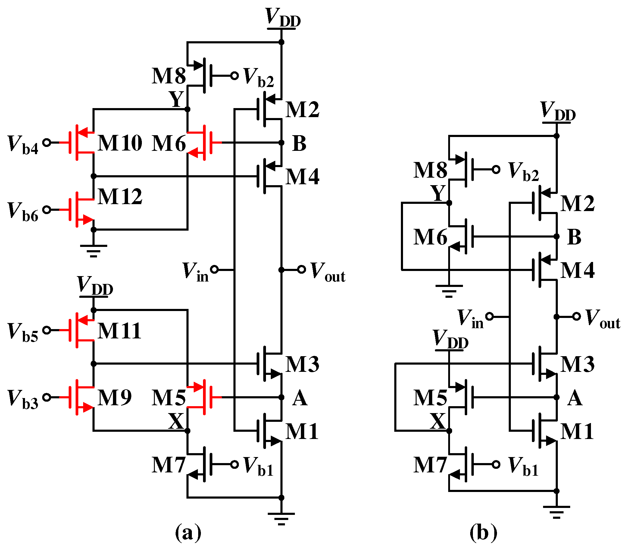
Figure 1a shows the conventional gain-boost inverter in [16,17]. Based on the simple cascode inverter shown in Figure 1b, the conventional gain-boost inverter introduces two gain-boost modules (transistors M5~M8). The two modules build up two feedback loops together with transistors M3 and M4, respectively. The DC gain of the conventional gain-boost inverter can be expressed as follows:
The DC gain of the simple cascode inverter can be expressed as follows:
Comparing Equations (1) and (2), it can be found that the introduction of the gain-boost modules increases the output impedance. Consequently, the DC gain of the conventional gain-boost inverter is also enhanced.
However, to make M5 and M6 operate in the saturation region, VA and VB must be larger than Vth5 and Vth6 (threshold voltage of M5 and M6). In a 180 nm CMOS process, the typical value of Vth is approximately 400~600 mV. In this case, the output swing of the conventional gain-boost inverter can be expressed as follows:
Vsat1 and Vsat2 represent the drain-source saturation voltage of M1 and M2, with values approximately equal to 3~4 VT (thermal voltage, with a value of 27 mV). The output swing of the simple cascode inverter can be expressed as follows:
Comparing Equations (3) and (4), it can be found that the output swing of the conventional structure is determined by VA and VB, resulting in a severe output-swing reduction.
To ease this reduction, the conventional gain-boost inverter uses low-Vth devices for M5 and M6, but this approach cannot solve the reduction in principle and will increase process complexity.
2.2. Proposed Output Swing-Enhanced Gain-Boost Inverter
Figure 2a depicts the proposed output swing-enhanced gain-boost inverter. There are three merits that come with this structure, as follows:
- The gain-boost modules used in the proposed gain-boost inverter have a folded-cascode structure, rather than common-source structure used in the conventional gain-boost inverter. The DC gain of the proposed structure can be expressed as follows:
Compared to Equation (1), the folded-cascode structure provides a higher output impedance, so the DC gain of the proposed gain-boost inverter is further enhanced.
- Compared to the conventional structure, M5 changes from NMOS to PMOS, and M6 changes from PMOS to NMOS. At this point, VA and VB are free from the restriction of Vth, and the minimum value of VA and VB could be Vsat again. As a result, the output swing is enhanced and can be expressed as follows:
Compared to Equation (2), the output-swing reduction is completely overcome.
- The existence of the two branches composed of M9~M12 enables the use of regular-Vth devices throughout the entire structure. If the two branches disappear, as shown in Figure 2b, the drains of M5 and M6 will directly connect to the gates of M3 and M4, respectively. The condition for M3 to M6 to operate in the saturation region is expressed as follows:
Equation (8) can be obtained after derivation:
In order to keep M3 to M6 operating in the saturation region and maintain a high DC gain, M5 and M6 need to employ high-Vth devices. The presence of M9–M12 creates a level shift from the source to the drain, separating the gates of M3 and M4 from the drains of M5 and M6. As a result, M5 and M6 can also be guaranteed to operate in the saturated region using regular-Vth devices, which can lower the process complexity of the proposed structure.
Figure 3a shows the frequency-response simulation circuit, and Figure 3b is the frequency-response simulation result of the proposed output swing-enhanced gain-boost inverter. It can be seen that the proposed structure reaches a DC gain of 91 dB with a 2.2 MHz gain bandwidth product (GBW), which meets the modulator’s requirement of DC gain for OTA discussed in Section 3.
Figure 4 shows the simulation result of the output swing versus the DC gain of the conventional structure and the proposed one. As the selected process does not support low-Vth devices, all transistors in the conventional structure use regular-Vth devices. The conventional structure can maintain a DC gain larger than 60 dB over a voltage range of 0.35 V to 0.81 V, resulting in an output swing of 0.46 V. In contrast, the proposed structure can achieve a 0.87 V output swing (from 0.18 V to 1.05 V), representing a 90% improvement.
Table 1 compares the proposed structure with the conventional structure using low-Vth devices in [13]. It can be observed that the DC gain is 8 dB higher than the conventional structure, and the output swing realizes a 24% improvement. The supply voltage and power consumption of the proposed structure are 1.2 V and 14.5 μW, respectively.
3. Topology Design of the Proposed DTDSM
To demonstrate the performance advantage of the proposed output swing-enhanced gain-boost inverter, a DTDSM is designed. The main specifications of the proposed modulator are summarized in Table 2.
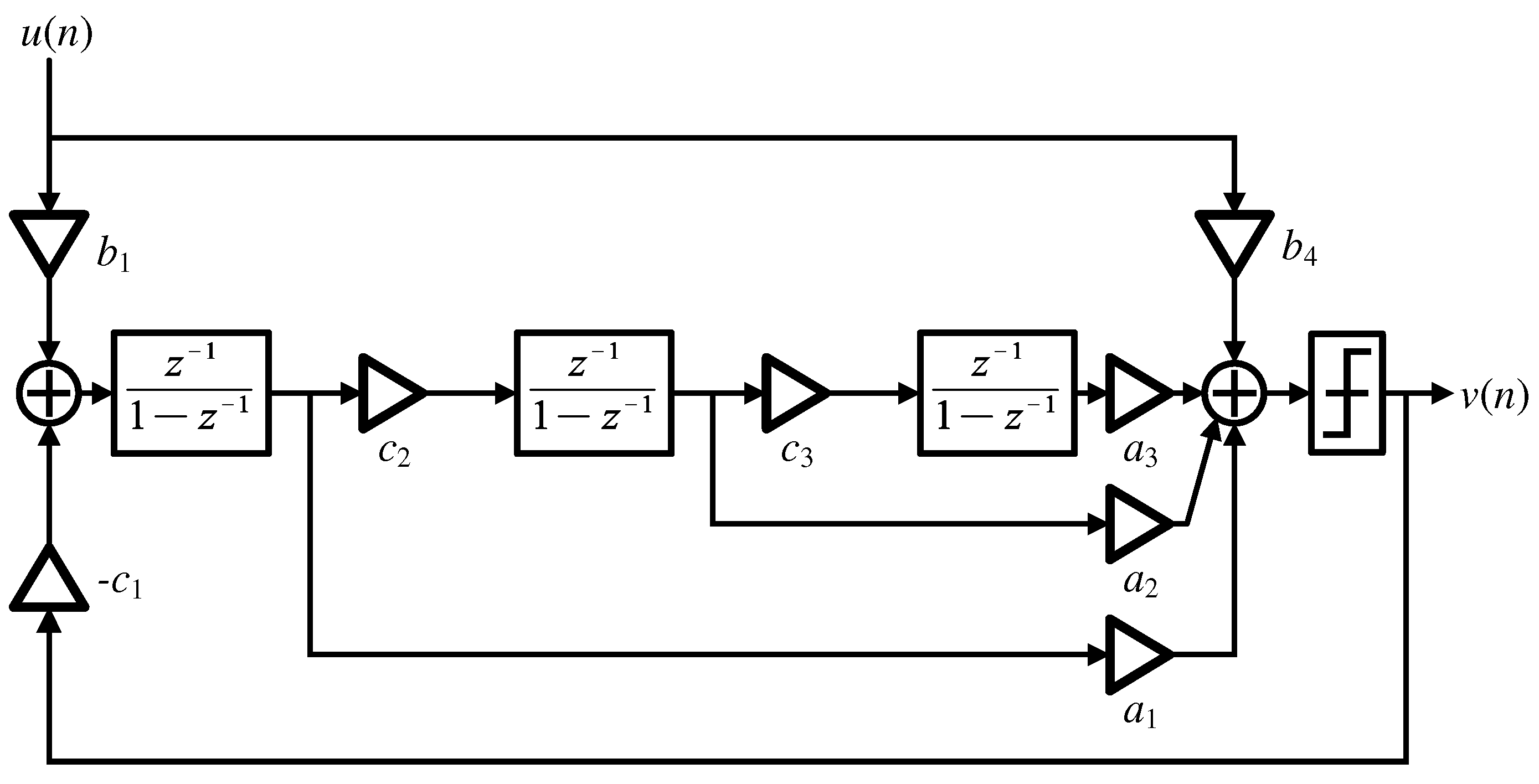
The first step is to choose an appropriate topology for the DTDSM. As discussed above, low voltage, low power consumption and high energy efficiency are significant. Compared to the cascade structure, the single-loop structure has lower distortion and is less affected by non-ideal factors of OTAs. In the feedforward structure, the input signal of the first-stage integrator is the difference between the input signal of the modulator and the feedback DAC signal, which is referred to as the residual signal. Compared to the feedback structure, the output swing of each stage of integrator is smaller. Therefore, the feedforward structure is more suitable for low-voltage design. Compared to the nonlinearity caused by a multi-bit quantizer, a single-bit quantizer has inherent higher linearity and a simpler structure, leading to lower power consumption [19]. After comprehensive consideration, this article opts to utilize a single-loop, third-order, feedforward single-bit topology, as illustrated in Figure 5.
Since the finite DC gain of the OTA used in the first-stage integrator will affect the overall performance of the modulator, it is necessary to analyze it. The classic switched-capacitor integrator is shown in Figure 6. The working process is divided into two phases: sampling (when φ1 is high level) and integrating (when φ2 is high level). Taking nth period as the analysis object. During sampling phase, the charge on CS and CI can be expressed as:
During integrating phase, the charge on CS and CI can be expressed as:
Since there is no charge leakage during the whole working process, it is obvious that:
After z-transformation, Equation (12) can be obtained as:
From the above derivation, it can be seen that the effect of the finite DC gain of the OTA on the integrator includes two parts: gain error and pole shift. Usually, the gain of the OTA is large, so the influence of the gain error is relatively small. However, pole shift affects the pole position of the integrator transfer function; this shift of the pole will introduce the leakage of in-band noise and eventually cause a decrease in the SNR of the modulator.
Through behavioral modeling and simulation, the relationship between the DC gain of the OTA used in the first-stage integrator and SNR can be obtained, as shown in Figure 7. When the DC gain is greater than 60 dB, the SNR of the modulator tends to be stable, so the DC gain of the OTA used in the first-stage integrator of the third-order modulator designed in this paper should larger than 60 dB. According to Figure 2, the proposed output swing-enhanced inverter can achieve a 91 dB peak DC gain, which meets the gain requirement.
The next step is to determine the values of the structure coefficients in Figure 5. The noise-transfer function (NTF) of Figure 5 can be calculated as follows:
Since c1, c2, and c3 affect the output swing of each stage of integrator, a parameter scan can be performed on the basis of determining the value of c1, c2, and c3 to finally obtain the values of the rest of the coefficients. Based on the calculation results, the coefficients of the designed modulator are summarized in Table 3. All the coefficients are realized in the form of fractions, and the numerator and denominator are integers, which is because the coefficients are realized by the ratio between capacitors in the actual circuit, such as the integrator coefficient corresponding to the ratio of sampling capacitor and integrating capacitor. Thus, capacitance matching can be better achieved by writing these coefficients in the form of easily realized fractions, reducing the error caused by capacitor mismatch.
Figure 8 shows the behavior simulation results of the outputs of each stage of integrator in the modulator under a −3 dBFS sinusoidal input signal. It can be seen that the output swing of the first-stage integrator is limited to 60% of the full-scale voltage. According to Table 1, the proposed gain-boost inverter can maintain a gain of more than 60 dB in the range of 73% full-scale voltage, so it is perfectly suitable for the modulator. Meanwhile, the output swings of the second- and third-stage integrators are relatively small, making the implementation of the second- and third-stage amplifiers easier. This is conducive to reducing the overall power consumption.
4. Circuit Implementation
Despite the third-order, feedforward, single-bit DTDSM, an oscillator and a current reference are also designed to ensure functional integrity.
4.1. Third-Order Delta-Sigma Modulator
As shown in Figure 9, the third-order, feedforward, single-bit modulator is depicted, comprising three inverter-based integrators, a passive adder, and a single-bit quantizer. In order to meet the noise requirements, the sampling capacitor of the first-stage integrator CS1 can be calculated according to the following formula:
where k is the Boltzmann constant and T is the absolute temperature. To ensure there is enough of a design margin, the sampling capacitor is set to 4.32 pF. All capacitor values in the circuit were calculated, and they are summarized in Table 4. It should be noted that the CS1 needs 21.6 pF, which occupies the largest area.
4.1.1. Inverter-Based Integrator
The structures of the three inverter-based integrators are all pseudo-differential, as depicted in Figure 9. The first integrator utilizes the proposed gain-boost inverter, as shown in Figure 2a, for optimal performance. To reduce the power dissipation, the second and third integrators adopt the simple cascode inverter, as shown in Figure 1b. An auto-zeroing technique is also introduced [20]. During the φ1 phase, the offset voltage is sampled in capacitor Cc. During the φ2 phase, the input node of the inverter is forced to become a virtual ground, thereby reducing the offset voltage and flicker noise.
To stabilize the output common-mode voltage of integrators at each stage, a low-voltage common-mode feedback (CMFB) loop is formed through capacitor CM. The advantages of this structure are no additional output load and the restriction of the output swing of the integrator [21].
4.1.2. Bootstrap Switch
In order to improve the linearity of the sampled signal, we utilize a low-voltage bootstrap switches, as depicted in Figure 10 [22], for all switches directly connected to the input signal. By pre-charging capacitor Cboost when the switch is off, the gate-source voltage of M1 can be maintained at a constant VDD when the switch is on. Therefore, the switch-on resistance of M1 can be expressed as follows:
This is independent from input signal Vin. Figure 11 shows the output spectrum of the bootstrap switch. It can be calculated that the SFDR and THD are 97.3 dB and 94.4 dB, respectively.
4.1.3. Single-Bit Quantizer
The comparator is mainly divided into static and dynamic structures. The static structure has a constant current, while the dynamic structure is controlled by the clock, resulting in lower power consumption compared to the static structure. This article focuses on the low-power design of the comparator. Therefore, the two-stage single-bit dynamic comparator shown in Figure 12 is utilized. The first stage is a StrongARM dynamic amplifier [23], and the second stage is an SR latch. When the control signal ENN is set to a low level, the comparator is reset, and the quantization result remains unchanged. When ENN is set to a high level, the comparator initiates the quantization operation. The difference between the differential input pairs is amplified rail-to-rail by the positive feedback loop composed of M3-M6. The quantization result is latched by the second stage.
4.2. Oscillator
The oscillator provides a stable control-clock signal for the entire modulator. For this design, the oscillator needs to meet requirements for low voltage and low power. Therefore, the relaxation oscillator shown in Figure 13 is adopted [24]. The structure generates a clock signal of corresponding frequency by repeatedly charging and discharging capacitors C1 and C2 and constantly flipping the output of the comparator. The simulation results of the oscillator are shown in Figure 14. A 1.1 MHz clock under 1.2 V supply voltage is realized, and the power consumption is 2.4 μW.
4.3. Current Reference
As depicted in Figure 2a and Figure 9, both the proposed output swing-enhanced inverter and the oscillator require a precise bias current. Therefore, a current reference is also designed, as shown in Figure 15 [25]. To achieve low-voltage operation and low power consumption, all transistors work in the subthreshold region. In this design, the relationship between the threshold voltage and the channel length is used to achieve the subtle difference between Vth1 and Vth2 (the channel length of M1 and M2 is bL and L, respectively). The existence of M4 and M5 forces the current flowing through M1 and M2 to be equal, which makes Vgs2 − Vgs1 equal to Vth2 − Vth1. Therefore, the reference current can be expressed as:
where Vth0,1 and Vth0,2 represent the threshold voltages of M1 and M2 at 0 K temperature, respectively. Meanwhile, a1 and a2 denote the temperature coefficients of the threshold voltages of M1 and M2, respectively. Since a1 and a2 are approximately equal and Vth0 is a constant value, the difference eliminates the temperature coefficient of Vth. Therefore, Iref can be temperature-independent if R1 has a small temperature coefficient.
The third branch, composed of M3 and M6, forces the voltages of nodes A and B to be equal. This guarantees the current accuracy and significantly enhances the line regulation of Iref through this additional feedback loop.
Figure 16 shows the simulation result of the low-voltage current reference. It can be seen that the current reference achieves a 1 μA current and a 26 ppm temperature drift in the range of −55~125 °C.
5. Results
The proposed chip is implemented in a 180 nm CMOS process. The microphotograph of the chip is presented in Figure 17, with the layout occupying a core area of 0.405 mm2 (900 μm × 450 μm).
Figure 18 shows the test board of the DSM. The power supply part includes an ultra-low-noise linear regulator (LT3045, Analog Devices, Norwood, MA, USA) and a high-precision, low-noise reference (AD780, Analog Devices, Norwood, MA, USA), which, in combination with Agilent, generates a 1.2 V supply voltage and a 0.6 V common mode voltage. A single-ended sinusoidal input signal is generated by a signal generator (Keysight 33600A, Keysight, Santa Rosa, CA, USA). The single-ended input to a differential output circuit in the signal input part changes it into a sinusoidal input signal. The single-ended input to differential output circuit is based on a low-noise fully differential amplifier (THS4551, Texas Instrument, Dallas, TX, USA). The digital output is captured and stored in the logic analyzer (Agilent 16810A, Keysight, Santa Rosa, CA, USA) and then sent to a PC for data processing.
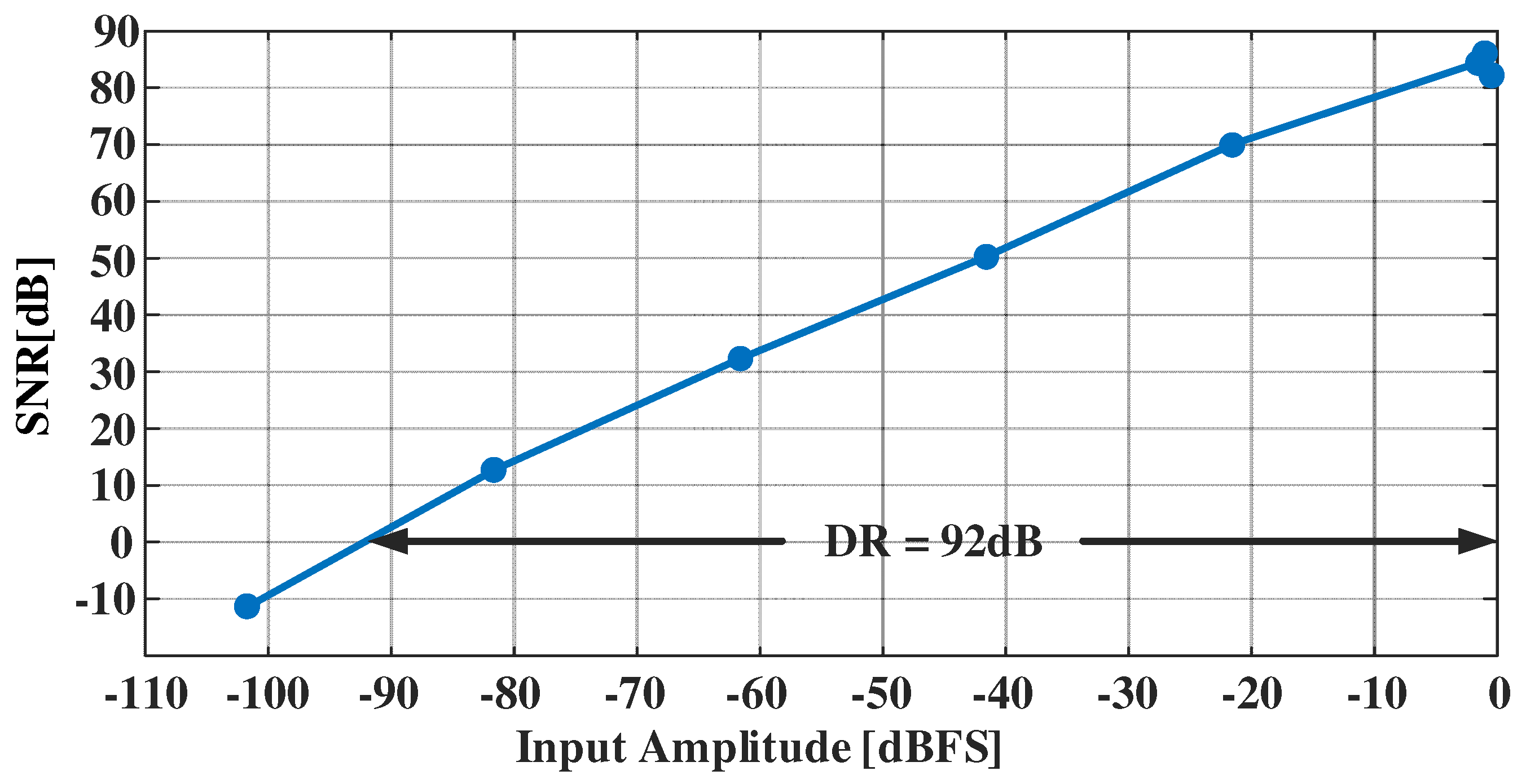
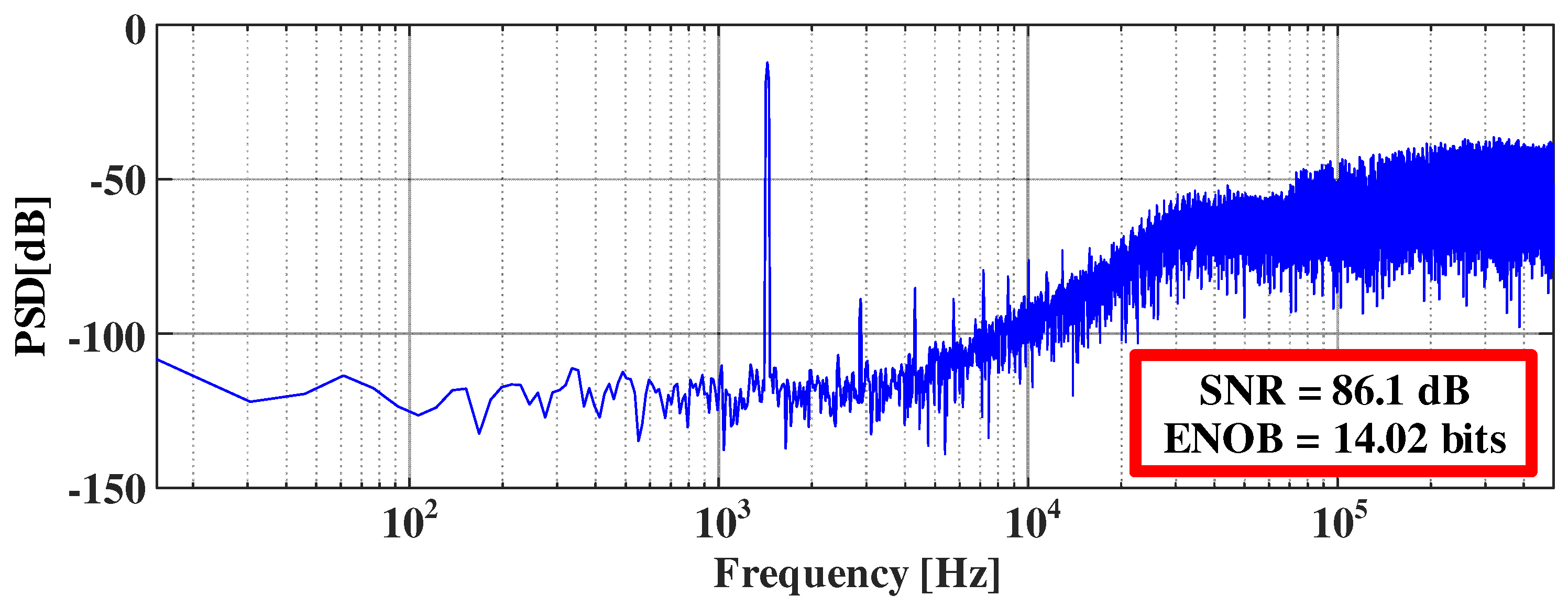
The output spectrum of the proposed modulator is displayed in Figure 19, with a 1.1 Vp-p, 1.4 kHz sinusoidal input signal. It can be observed that the noise floor is −120 dB. The SNR is 86.1 dB. Figure 20 illustrates the measured SNR versus the input signal amplitudes normalized by full-scale voltage. It is evident that the modulator achieves a 92 dB DR. The total power consumption is 54.5 μW.
As mentioned above, using FoMs to fairly compare the overall performance of different modulators [6]:
where BW represents the signal bandwidth and Power represents the total power consumption of the chip. The proposed modulator achieves a 167.6 dB FoMs. The results in [18] are pre-simulation results. Compared to [18], the FoMs drop is mainly caused by the following reasons:
- The reduction of SNR is due to the transient noise introduced by devices (mainly MOS, capacitors and resistors) and various parasitic parameters introduced by the layout.
- There is increased noise and power consumption introduced by the current reference and oscillators.
The performance of the proposed modulator is also compared with other published modulators with a supply near 1.2 V in Table 5. It can be observed that the proposed modulator is competitive in FoMs.
6. Conclusions
In summary, this article presents a third-order, feedforward, single-bit, delta-sigma analog-to-digital modulator (DSM) based on an output swing-enhanced gain-boost inverter. The proposed output swing-enhanced inverter addresses the output-swing reduction issue of the conventional gain-boost inverter in principle. Therefore, high DC gain and a large output swing can be realized simultaneously. Fabricated in a 180 nm CMOS process, the whole chip contains a delta-sigma modulator, an oscillator, and a current reference. The modulator achieves an 86.1 dB peak SNR with a 1.4 kHz sinusoidal input signal. The DR is 92 dB, and the signal bandwidth is 1.95 kHz. The entire chip dissipates 54.5 μW, leading to 167.6 dB FoMs, and shows competitiveness compared with other modulators with a supply near 1.2 V.
Author Contributions
Conceptualization, W.L.; methodology, T.Z.; validation, G.L.; writing—original draft preparation, H.W.; writing—review and editing, J.L. All authors have read and agreed to the published version of the manuscript.
Funding
This research received no external funding.
Data Availability Statement
Data are available on request due to restrictions on privacy. The data presented in this study are available upon request from the corresponding author. The data are not publicly available as the project discussed in this study is still in development.
Conflicts of Interest
The authors declare no conflicts of interest.
References
- De la Rosa, J.M.; Schreier, R.; Pun, K.-P.; Pavan, S. Next-generation delta-sigma converters: Trends and perspectives. IEEE J. Emerg. Sel. Top. Circuits Syst. 2015, 5, 484–499. [Google Scholar] [CrossRef]
- Yazicioglu, R.; Merken, P.; van Hoof, C. 200 μW eight-channel acquisition ASIC for ambulator EEG systems. In Proceedings of the IEEE International Solid-State Circuits Conference, San Francisco, CA, USA, 3–7 February 2008; Volume 164. [Google Scholar]
- Pisha, L.; Warchall, J.; Zubatiy, T.; Hamilton, S.; Lee, C.-H.; Chockalingam, G.; Mercier, P.P.; Gupta, R.; Rao, B.D.; Garudadri, H. A wearable, extensible, open-source platform for hearing healthcare research. IEEE Access 2019, 7, 162083–162101. [Google Scholar] [CrossRef] [PubMed]
- Ma, S.; Liu, L.; Fang, T.; Liu, J.; Wu, N. A Discrete-Time Audio ΔΣ Modulator Using Dynamic Amplifier with Speed Enhancement and Flicker Noise Reduction Techniques. IEEE J. Solid-State Circuits 2019, 55, 333–343. [Google Scholar] [CrossRef]
- An, K.-C.; Narasimman, N.; Kim, T.T.-H. A 0.6-to-1.2 V Scaling Friendly Discrete-Time OTA-Free ΔΣ-ADC for IoT Applications. In Proceedings of the ESSCIRC 2021-IEEE 47th European Solid State Circuits Conference (ESSCIRC), Grenoble, France, 13–22 September 2021. [Google Scholar]
- Pavan, S.; Schreier, R.; Temes, G.C. Understanding Delta-Sigma Data Converters; John Wiley & Sons: Hoboken, NJ, USA, 2017. [Google Scholar]
- Lopez-Martin, A.; Algueta, J.M.; Garde, M.P.; Carvajal, R.G.; Ramirez-Angulo, J. 1-V 15-μW 130-nm CMOS Super Class AB OTA. In Proceedings of the 2020 IEEE International Symposium on Circuits and Systems (ISCAS), Seville, Spain, 12–14 October 2020. [Google Scholar]
- Cabrera-Bernal, E.; Pennisi, S.; Grasso, A.D.; Torralba, A.; Carvajal, R.G. 0.7-V three-stage class-AB CMOS operational transconductance amplifier. IEEE Trans. Circuits Syst. I Regul. Pap. 2016, 63, 1807–1815. [Google Scholar] [CrossRef]
- Kulej, T.; Khateb, F. A compact 0.3-V class AB bulk-driven OTA. IEEE Trans. Very Larg. Scale Integr. (VLSI) Syst. 2019, 28, 224–232. [Google Scholar] [CrossRef]
- Kumar, R.A.; Krishnapura, N.; Banerjee, P. Analysis and design of a discrete-time delta-sigma modulator using a cascoded floating-inverter-based dynamic amplifier. IEEE J. Solid-State Circuits 2022, 57, 3384–3395. [Google Scholar] [CrossRef]
- Zhao, M.; Zhao, Y.; Zhang, H.; Hu, Y.; Bao, Y.; Ye, L.; Qu, W.; Tan, Z. A 4-μW Bandwidth/Power Scalable Delta–Sigma Modulator Based on Swing-Enhanced Floating Inverter Amplifiers. IEEE J. Solid-State Circuits 2021, 57, 709–718. [Google Scholar] [CrossRef]
- De Aguirre, P.C.C.; Bonizzoni, E.; Maloberti, F.; Susin, A.A. A 170.7-dB FoM-DR 0.45/0.6-V inverter-based continuous-time sigma–delta modulator. IEEE Trans. Circuits Syst. II Express Briefs 2019, 67, 1384–1388. [Google Scholar] [CrossRef]
- Wei, R.; Wang, W.; Xiao, X.; Chen, Q. A low-power delta-sigma capacitance-to-digital converter for capacitive sensors. IEEE Access 2019, 7, 78281–78288. [Google Scholar] [CrossRef]
- Wang, Z.; Duan, Q.; Roh, J. A 0.03 mm2 delta-sigma modulator with cascaded-inverter amplifier. Analog Integr. Circuits Signal Process. 2014, 81, 495–501. [Google Scholar] [CrossRef]
- Conrad, J.; Vogelmann, P.; Mokhtar, M.A.; Ortmanns, M. Design approach for ring amplifiers. IEEE Trans. Circuits Syst. I Regul. Pap. 2020, 67, 3444–3457. [Google Scholar] [CrossRef]
- Luo, H.; Han, Y.; Cheung, R.C.; Cao, T.; Liu, X.; Gao, F. A ΣΔ modulator using gain-boost class-C inverter for audio applications. J. Circuits Syst. Comput. 2013, 22, 1340024. [Google Scholar] [CrossRef]
- Luo, H.; Han, Y.; Cheung, R.C.; Liu, X.; Cao, T. A 0.8-V 230-μW 98-dB DR Inverter-Based ΣΔ Modulator for Audio Applications. IEEE J. Solid-State Circuits 2013, 48, 2430–2441. [Google Scholar] [CrossRef]
- Wu, H.; Li, W.; Liu, J.; Zhang, T. A 1-V 109.1-dB SNDR 185.2-dB FoMs DSM Based on An Output Swing Enhanced Gain-Boost Inverter. In Proceedings of the 2022 7th International Conference on Integrated Circuits and Microsystems (ICICM), Xi’an, China, 28–31 October 2022; IEEE: New York, NY, USA, 2023. [Google Scholar]
- De la Rosa, J.M.; Del Rio, R. CMOS Sigma-Delta Converters: Practical Design Guide; John Wiley & Sons: Hoboken, NJ, USA, 2013. [Google Scholar]
- Chae, Y.; Han, G. Low voltage, low power, inverter-based switched-capacitor delta-sigma modulator. IEEE J. Solid-State Circuits 2009, 44, 458–472. [Google Scholar] [CrossRef]
- Chae, Y.; Cheon, J.; Lim, S.; Kwon, M.; Yoo, K.; Jung, W.; Lee, D.-H.; Ham, S.; Han, G. A 2.1 M Pixels, 120 Frame/s CMOS Image Sensor With Column-Parallel ΔΣ ADC Architecture. IEEE J. Solid-State Circuits 2010, 46, 236–247. [Google Scholar] [CrossRef]
- Chen, H.; He, L.; Deng, H.; Yin, Y.; Lin, F. A high-performance bootstrap switch for low voltage switched-capacitor circuits. In Proceedings of the 2014 IEEE International Symposium on Radio-Frequency Integration Technology, Hefei, China, 27–30 August 2014. [Google Scholar]
- Razavi, B. The Strong ARM latch [a circuit for all seasons]. IEEE Solid-State Circuits Mag. 2015, 7, 12–17. [Google Scholar]
- Wang, L.; Zhan, C.; Zhang, Z.; Zhao, S. A−40–125° C, 0.8 V, 33 kHz relaxation oscillator with integrated voltage and current reference and compensated comparator delay. Microelectron. J. 2021, 117, 105285. [Google Scholar] [CrossRef]
- Hu, J.; Lu, C.; Xu, H.; Wang, J.; Liang, K.; Li, G. A novel precision CMOS current reference for IoT systems. AEU-Int. J. Electron. Commun. 2021, 130, 153577. [Google Scholar] [CrossRef]
- Lee, S.-Y.; Lee, H.-Y.; Kung, C.-H.; Su, P.-H.; Chen, J.-Y. A 0.8-μW and 74-dB High-Pass Sigma-Delta Modulator With OPAMP Sharing and Noise-Coupling Techniques for Biomedical Signal Acquisition. IEEE Trans. Biomed. Circuits Syst. 2022, 16, 742–751. [Google Scholar] [CrossRef] [PubMed]
- Boni, A.; Giuffredi, L.; Pietrini, G.; Ronchi, M.; Caselli, M. A low-power sigma-delta modulator for healthcare and medical diagnostic applications. IEEE Trans. Circuits Syst. I Regul. Pap. 2021, 69, 207–219. [Google Scholar] [CrossRef]
- Chen, X.; Wang, Z.-G.; Li, F. Design of A 1-V 3rd-order 1-bit Σ-Δ modulator with inverter-based static–dynamic hybrid structure amplifiers. Analog Integr. Circuits Signal Process. 2019, 101, 351–361. [Google Scholar] [CrossRef]
- Liang, J.; Sin, S.-W.; Seng-Pan, U.; Maloberti, F.; Martins, R.P.; Jiang, H. A high DR high-input-impedance programmable-gain ECG acquisition interface with non-inverting continuous time sigma-delta modulator. In Proceedings of the 2019 IEEE Asian Solid-State Circuits Conference (A-SSCC), Macau, Macao, 4–6 November 2019. [Google Scholar]
- Zhao, L.; Deng, C.; Wang, G.; Chen, H.; Cheng, Y. A 1.1 V 12 μW 86 dB DR sigma-delta modulator for health monitoring system. J. Circuits Syst. Comput. 2016, 25, 1650059. [Google Scholar] [CrossRef]
Figure 1.
(a) Conventional gain-boost inverter; (b) simple cascode inverter.
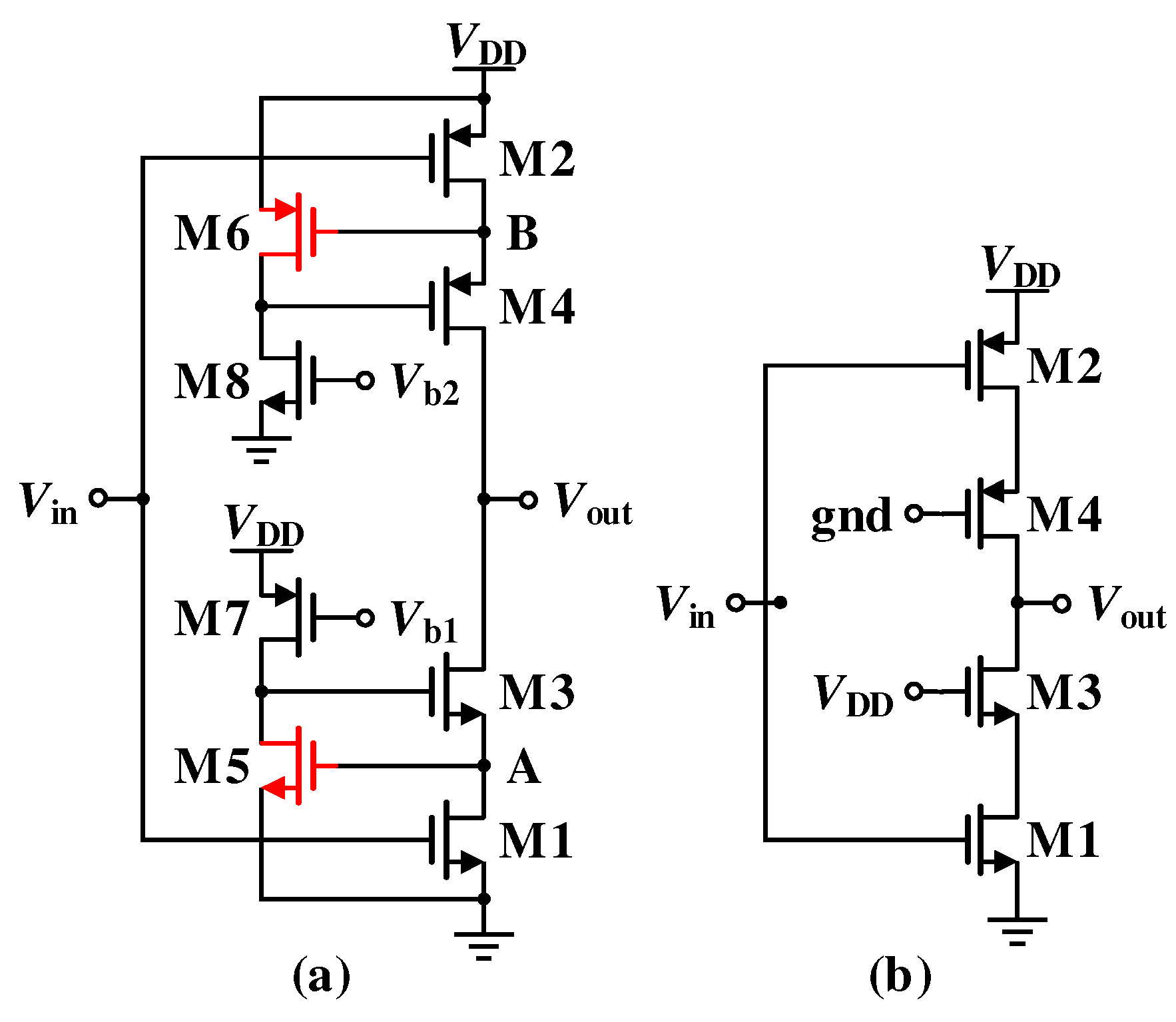
Figure 2.
(a) Proposed output swing-enhanced gain-boost inverter; (b) circuit without M9~M12.

Figure 3.
(a) Frequency-response simulation circuit and (b) simulation result of the frequency response of the proposed output swing-enhanced gain-boost inverter.
Figure 3.
(a) Frequency-response simulation circuit and (b) simulation result of the frequency response of the proposed output swing-enhanced gain-boost inverter.

Figure 4.
Simulation result of output swing versus DC gain.
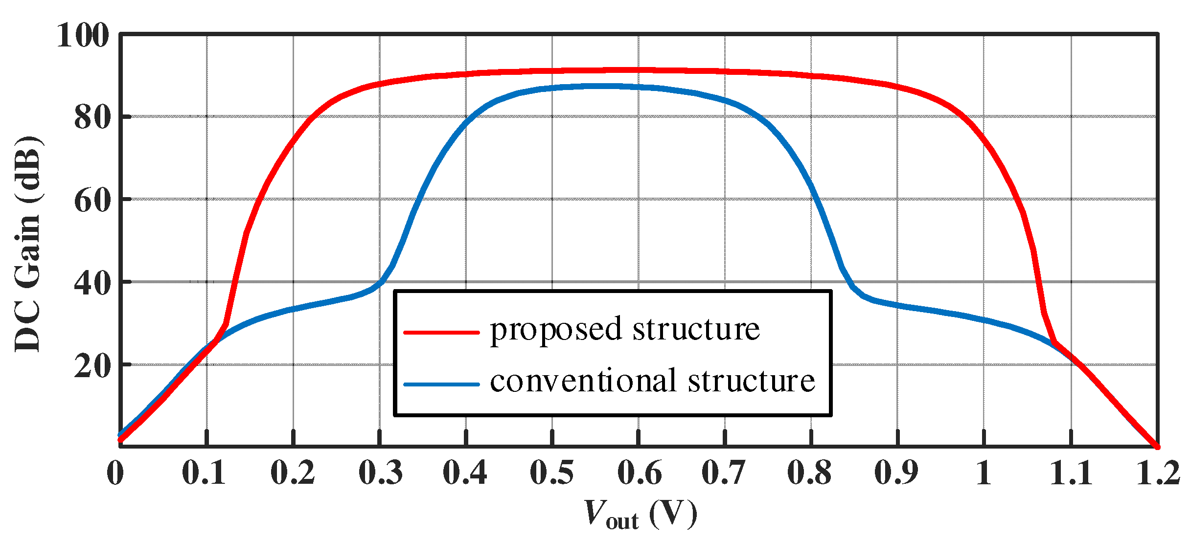
Figure 5.
Topology of the proposed Δ-Σ Modulator.

Figure 6.
The switch-capacitor integrator.
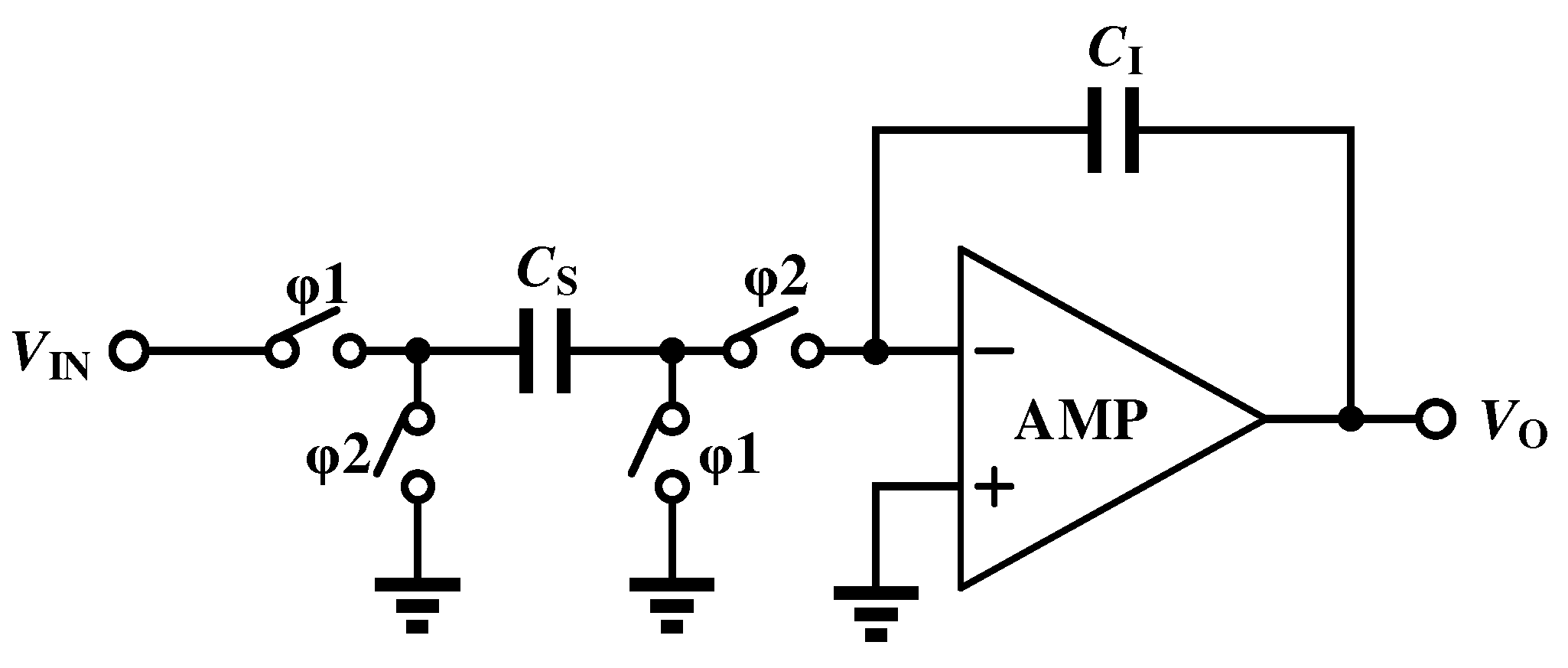
Figure 7.
The relationship between SNR and the DC gain of the OTA used in the first-stage integrator.
Figure 7.
The relationship between SNR and the DC gain of the OTA used in the first-stage integrator.
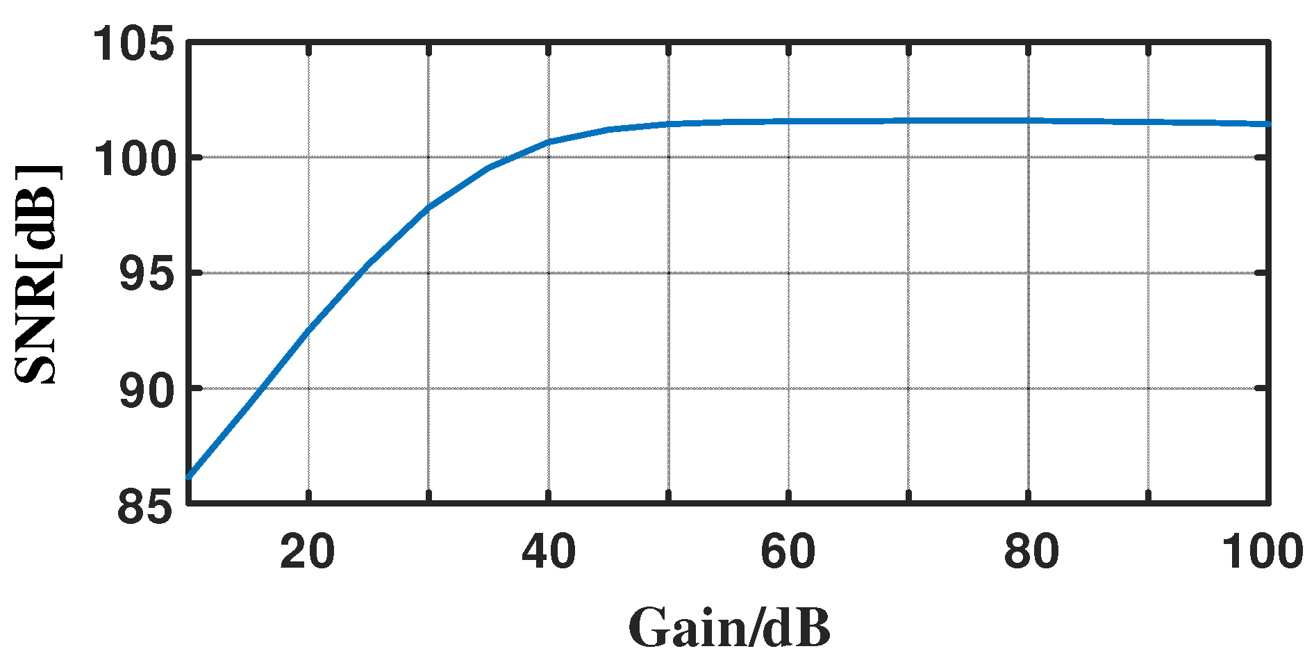
Figure 8.
The histogram of the integrator outputs.
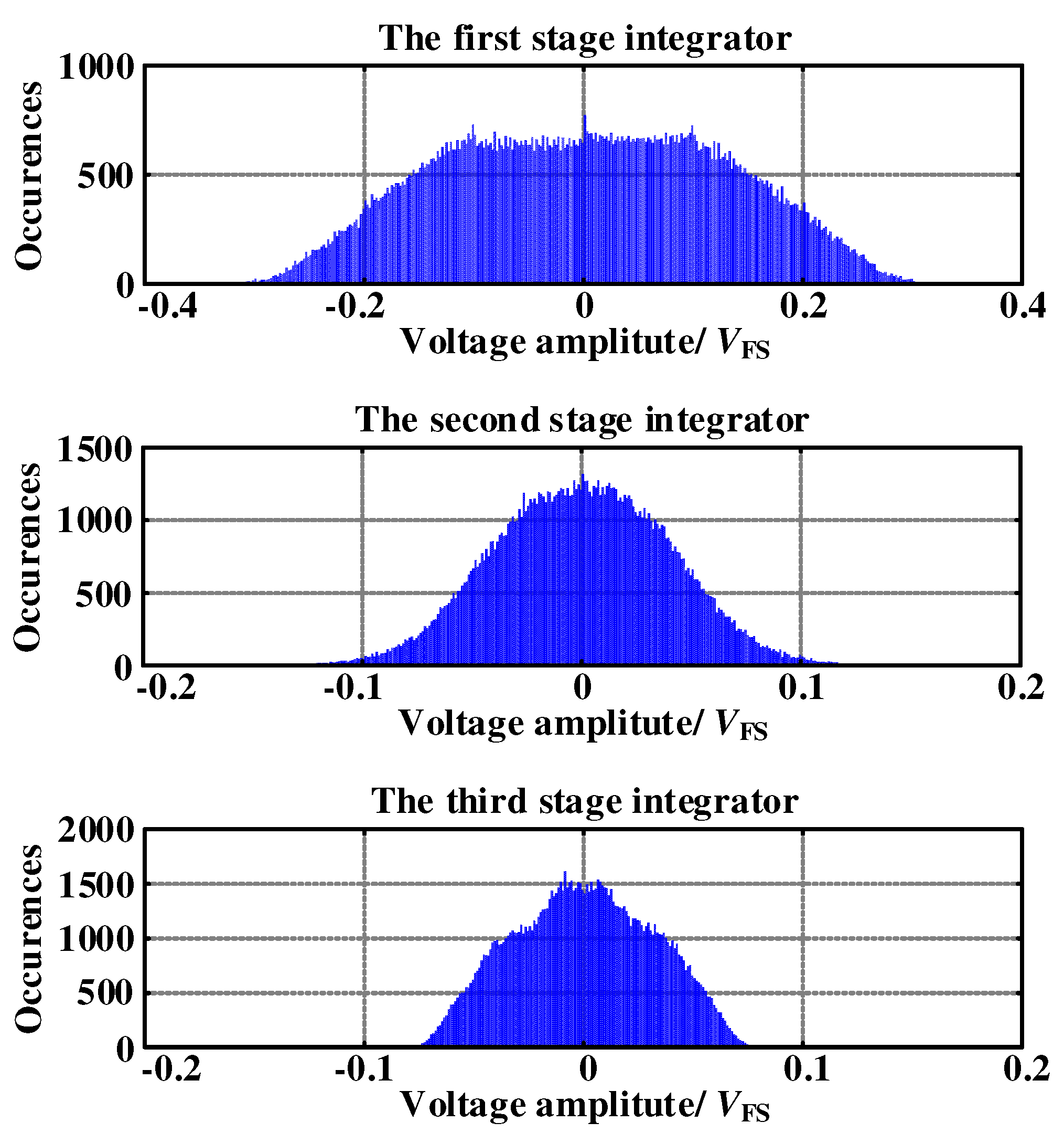
Figure 9.
Schematic of the proposed DTDSM.

Figure 10.
Schematic of the bootstrap switch.

Figure 11.
Output spectrum of the bootstrap switch.

Figure 12.
Schematic of the single-bit quantizer.

Figure 13.
Schematic of the low-voltage relaxation oscillator.

Figure 14.
Simulation result of the low-voltage relaxation oscillator.
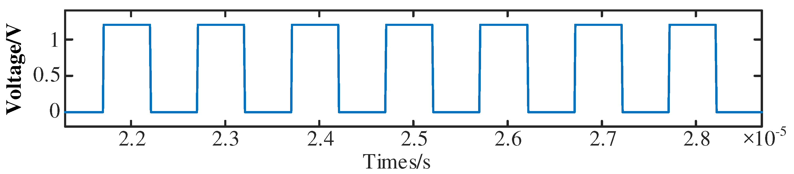
Figure 15.
Schematic of the low-voltage current reference.
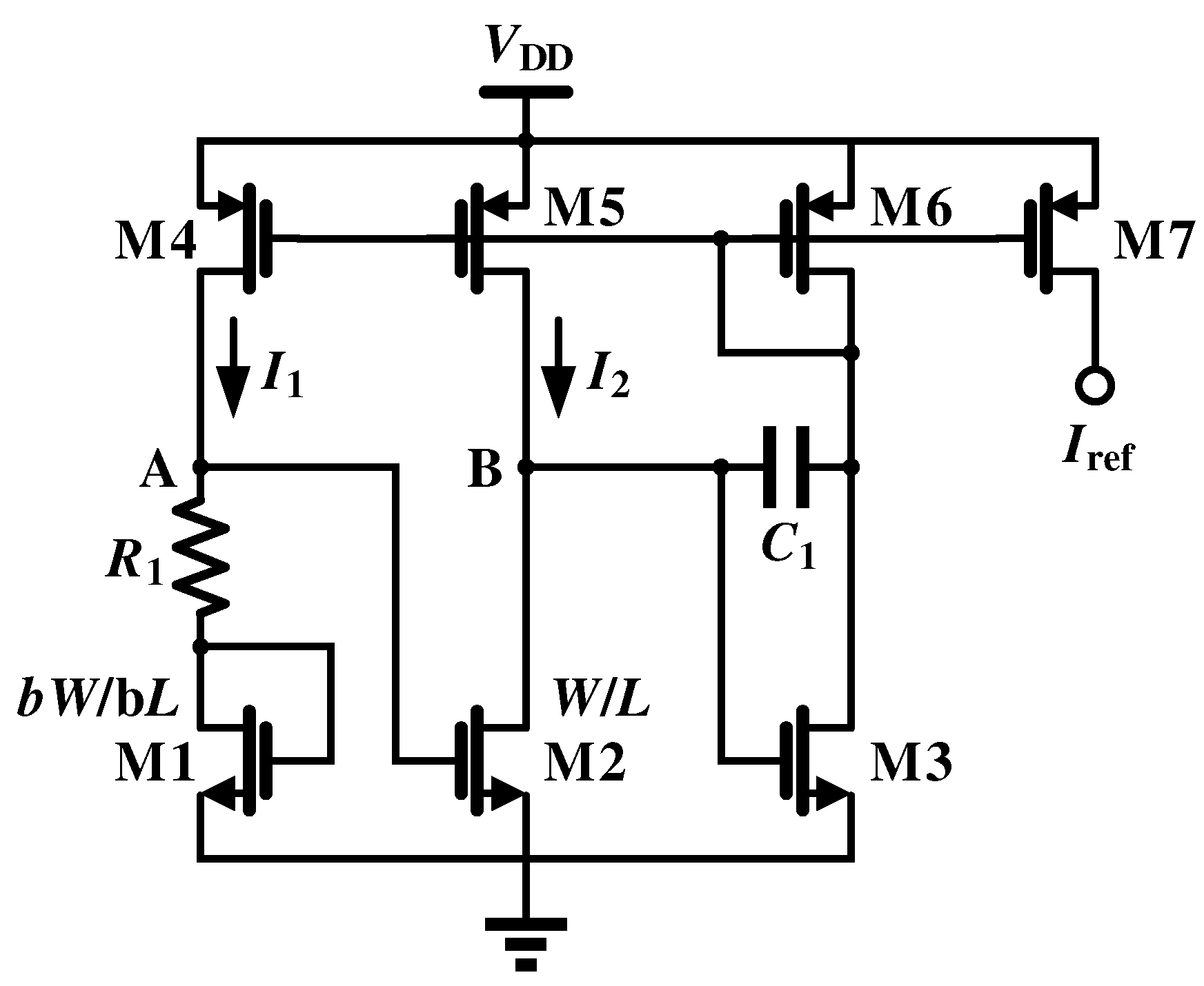
Figure 16.
Simulation result of the low-voltage current reference.

Figure 17.
The microphotograph of the chip.
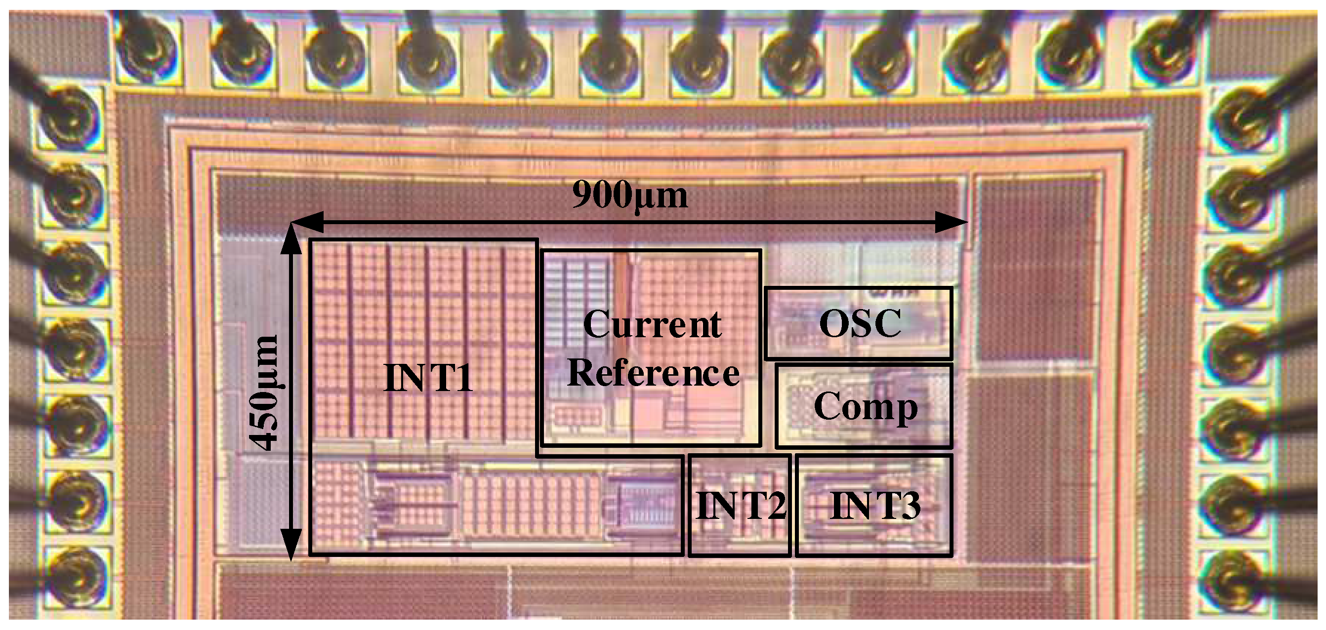
Figure 18.
The test board of the DSM.
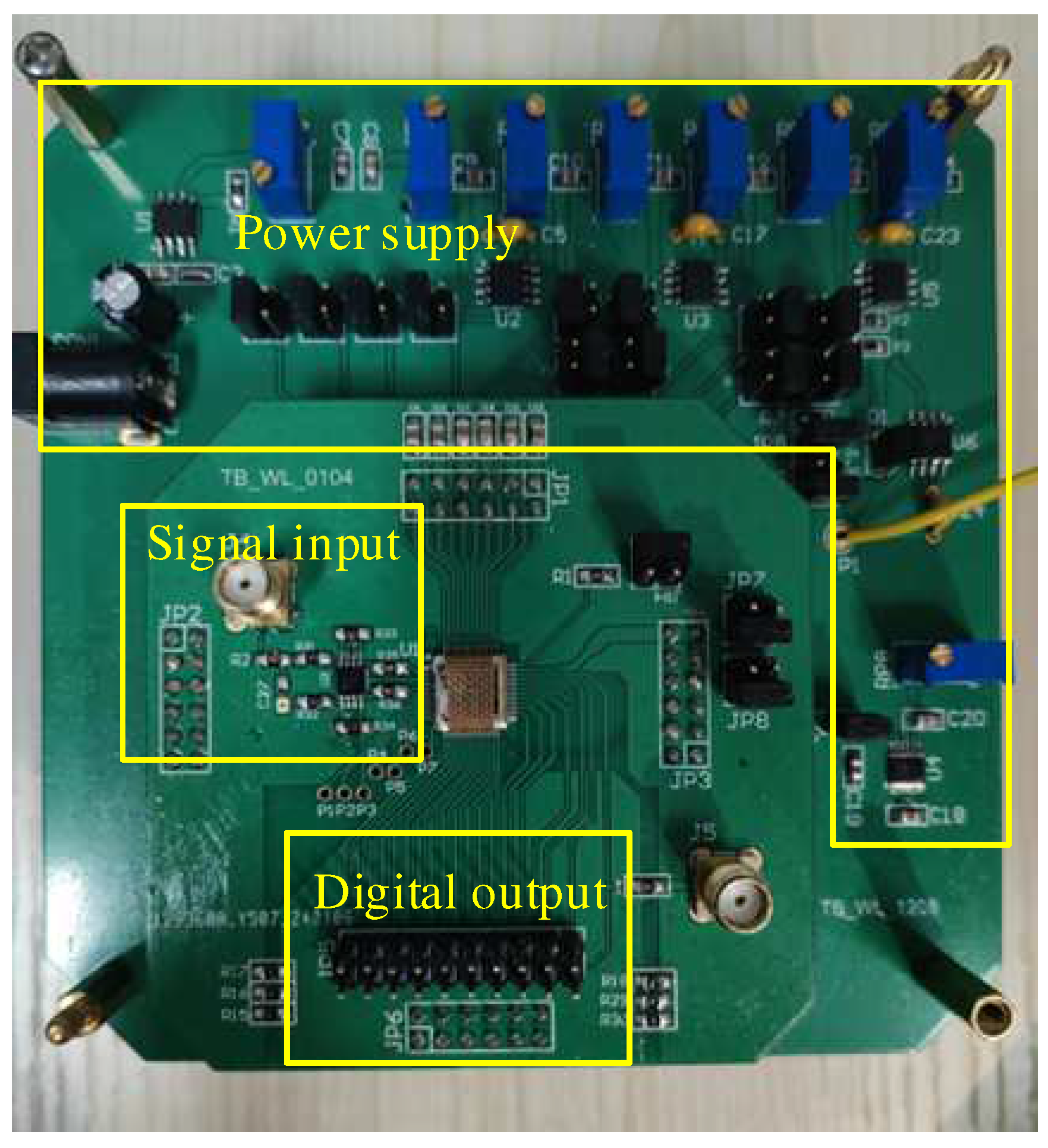
Figure 19.
The output spectrum of the proposed modulator.

Figure 20.
Measured SNR versus the input signal amplitudes normalized by full scale voltage.

Table 1.
DC gain versus output swing comparison.
| DC Gain/dB | Output Swing/V | Full-Scale Voltage/V | Full-Scale Ratio | |
|---|---|---|---|---|
| Conventional structure (without low-Vth devices) | 85 | 0.46 | 1.2 | 38% |
| Conventional structure in [13] (with low-Vth devices) | 83 | 0.59 | 1.2 | 59% |
| Proposed structure | 91 | 0.87 | 1.2 | 73% |
Table 2.
Main modulator specifications.
| Parameters | Value | Unit |
|---|---|---|
| Signal bandwidth (BW) | 1.95 | kHz |
| Oversampling ratio (OSR) | 256 | - |
| Sampling frequency | 1 | MHz |
| Full-scale (differential) | 1.2 | V |
| Supply voltage | 1.2 | V |
Table 3.
Coefficients of the designed modulator.
| Feedforward Coefficients | Signal Coefficients | Integrator Coefficients |
|---|---|---|
| a1 = 4 | b1 = 1/5 | c1 = 1/5 |
| a2 = 6 | b4 = 1 | c2 = 1/4 |
| a3 = 5 | c3 = 1/6 |
Table 4.
Capacitor values in the modulator.
| Sampling Capacitors/pF | Integrating Capacitors/pF | Feedforward Capacitors/pF | Common-Mode Capacitors/pF | Compensation Capacitors/pF |
|---|---|---|---|---|
| Cs1 = 4.32 | CI1 = 21.6 | CF1 = 0.05 | CM1 = 1 | Cc1 = 5 |
| Cs2 = 0.125 | CI2 = 0.5 | CF2 = 0.2 | CM2 = 0.16 | Cc2 = 1 |
| Cs3 = 0.08 | CI3 = 0.48 | CF3 = 0.3 | CM3 = 0.16 | Cc3 = 1 |
| CF4 = 0.25 |
Table 5.
Performance summary of the DSMs with a supply near 1.2 V.
| References | This Work | 2022 [26] | 2021 [27] | 2019 [28] | 2019 [29] | 2016 [30] |
|---|---|---|---|---|---|---|
| Architecture | DT | DT | DT | DT | CT | DT |
| Process/nm | 180 | 180 | 90 | 40 | 65 | 180 |
| Supply voltage/V | 1.2 | 1 | 1.2 | 1 | 1 | 1.1 |
| BW/kHz | 1.953 | 0.2 | 0.25 | 100 | 150 | 0.3 |
| OSR | 256 | 64 | 500 | 128 | 128 | 128 |
| DR/dB | 92 | 78.2 | 95.6 | 86.7 | 99.3 | 86 |
| SNR/dB | 86.1 | 75.26 | 93 | 89.7 | 84.2 | 85.9 |
| Power/μW | 54.5 | 0.8 | 30 | 860 | 20.8 | 12 |
| FoMs/dB | 167.6 | 162.18 | 164.8 | 167.4 | 167.8 | 160 |
Disclaimer/Publisher’s Note: The statements, opinions and data contained in all publications are solely those of the individual author(s) and contributor(s) and not of MDPI and/or the editor(s). MDPI and/or the editor(s) disclaim responsibility for any injury to people or property resulting from any ideas, methods, instructions or products referred to in the content. |
© 2024 by the authors. Licensee MDPI, Basel, Switzerland. This article is an open access article distributed under the terms and conditions of the Creative Commons Attribution (CC BY) license (https://creativecommons.org/licenses/by/4.0/).
Share and Cite
MDPI and ACS Style
Wu, H.; Li, W.; Zhang, T.; Li, G.; Liu, J. A 1.2 V, 92 dB Dynamic-Range Delta-Sigma Modulator Based on an Output Swing-Enhanced Gain-Boost Inverter. Electronics 2024, 13, 1570. https://doi.org/10.3390/electronics13081570
AMA Style
Wu H, Li W, Zhang T, Li G, Liu J. A 1.2 V, 92 dB Dynamic-Range Delta-Sigma Modulator Based on an Output Swing-Enhanced Gain-Boost Inverter. Electronics. 2024; 13(8):1570. https://doi.org/10.3390/electronics13081570
Chicago/Turabian StyleWu, Honghao, Wenchang Li, Tianyi Zhang, Guanqi Li, and Jian Liu. 2024. "A 1.2 V, 92 dB Dynamic-Range Delta-Sigma Modulator Based on an Output Swing-Enhanced Gain-Boost Inverter" Electronics 13, no. 8: 1570. https://doi.org/10.3390/electronics13081570
Note that from the first issue of 2016, this journal uses article numbers instead of page numbers. See further details here.