
Modeling and Control of an Inductive Power Transmitter Based on Buck–Half Bridge–Resonant Tank


ESIME Culhuacan, Instituto Politécnico Nacional, Av. Santa Ana 1000, Mexico City 04440, Mexico
*
Authors to whom correspondence should be addressed.
Electronics 2024, 13(8), 1593; https://doi.org/10.3390/electronics13081593
Submission received: 22 March 2024
/
Revised: 11 April 2024
/
Accepted: 19 April 2024
/
Published: 22 April 2024
Abstract
:In this paper, a previously proposed converter to be used for inductive wireless power transmission is modeled and a control strategy is proposed. The converter topology combines into a single stage, two buck converters and a half-bridge converter to feed a resonant stage. This simple and symmetrical topology is straightforward to design; only a buck converter and a parallel resonant tank must be specified. It would be desirable for the converter to feed a wide range of loads and be robust under input voltage variations. These objectives can not be attained with a linear model and control. For this reason, in this paper, a nonlinear converter model is derived step by step and controller strategy is developed without relying on system linearization. The proposed controller does not measure the output but only its peak value. This can be conducted because it takes advantage of the square current pulse fed into a resonant tank; it outputs an approximately sinusoidal signal. The control strategy is completed with a scheme to build the required pulse at the input of the resonant tank. The resulting nonlinear controller has a fast closed-loop performance; furthermore, it is robust under parameter uncertainty, and load and input voltage variations. Despite its features, the controller is fairly simple to implement.
1. Introduction
The fast-growing technology of wireless power transfer (WPT) [1,2,3], particularly for last-generation mobile devices, has driven the development of many mobile charger schemes. Among them, inductive wireless power transfer (IWPT) is suitable for hostile environments [4]. That is why the IWPT is among the most common way of WPT [5,6].
The IWPT uses an electromagnetic coupling consisting of two inductors with flat ferrite nuclei. The first inductor is on the transmitter and the second is on the receptor. The coupling is through the air, hence, the transmission is restricted to a small distance between transmission and reception inductors [7].
Inductive wireless transmission has been a very active area of research. It is now widely applied in implantable devices [8,9,10], electric vehicles [11,12], portable devices [13,14] and generally in all electronic equipment with batteries that must be temporarily charged [15].
Usually, IWPT systems have four basic parts: on the transmitter side there is a DC-DC converter, an inverter and a resonant stage for coupling; on the receptor side a high-frequency rectifier is needed [16].
To guarantee constant and stable energy transmission, an IWPT system should include a compensation scheme. Usually, one capacitor is added to the transmission inductor; this reduces the reactive power and increases the load capacity; hence, the efficiency is improved. Compensation schemes usually employed are series-series (SS), series-parallel, parallel-series and parallel-parallel; the name of the scheme refers to how the resonant capacitor is connected with the transmission inductor. The most common compensation scheme is the SS on the transmission side; on the receptor side a rectifier bridge is commonly used. The rectifier delivers a DC current to energize a resistive load. However, this scheme is not convenient when the load is an array of rechargeable batteries or supercapacitors, in these cases it is necessary to control the load current. To change the load current, the inverter output voltage has to be adjusted on the transmitter side, consequently, a model-based control strategy is required on the transmitter. In addition, the control strategy must be robust under load variation and it would be also convenient to be robust under input voltage variation. This paper is aimed to solve this control problem for the topology described below.
In this work, a topology that combines two buck converters, a half bridge, and a parallel resonant tank into a single stage to be used as a transmitter in an IWPT system is employed [16]. The symmetry of the topology simplifies the design; it is only necessary to design one buck converter and the resonant tank. The two buck converters feed the resonant tank with a square current signal, guaranteeing a sinusoidal voltage in the transmitter inductor, consequently the loss in the inductive coupling is significantly reduced.
A procedure to obtain a nonlinear mathematical model is presented; based on this model, a control strategy that does not rely on model linearization is proposed. To obtain the control strategy, indirect control ideas are used [17]. That means first the input current required at the parallel resonant part is determined, and then how to produce this current is investigated.
To produce a sinusoidal voltage at the output of a parallel resonant tank, the following fact is used: when the input of the tank is a square current pulse the output is approximately a sinusoidal voltage with the same frequency as its input. Thus, injecting a square pulse of current into the resonant tank yields the required sinusoidal output. Nevertheless, it is still necessary to know the current amplitude that must be injected. In the parallel resonant converter, the output amplitude depends on the load in a strongly nonlinear way. Hence, the amplitude of the square current at the input of the tank must be estimated dynamically. To this end, it is not necessary to measure the output voltage, only its peak value.
Once the necessary input current of the parallel resonant converter has been estimated, the switching policy for each buck converter is derived. Control expressions were developed to allow for fine-grain control of the energy transmitted to the load, enabling the transmitter to feed loads such as batteries and many other non-static loads. Yet, the controller is fairly simple to implement. Furthermore, the step-by-step derivation of the model and the control strategy enable the reader to model and control similar converters.
The paper is organized as follows, in Section 2 the converter topology is presented; operation modes are also described in this Section. In Section 3, the mathematical model is developed. An open-loop simulation is also presented in this Section. The control strategy is derived in Section 4. To evaluate the control strategy, closed-loop performance is simulated in this Section. Finally, some conclusions are presented in the last Section.
2. Converter Description
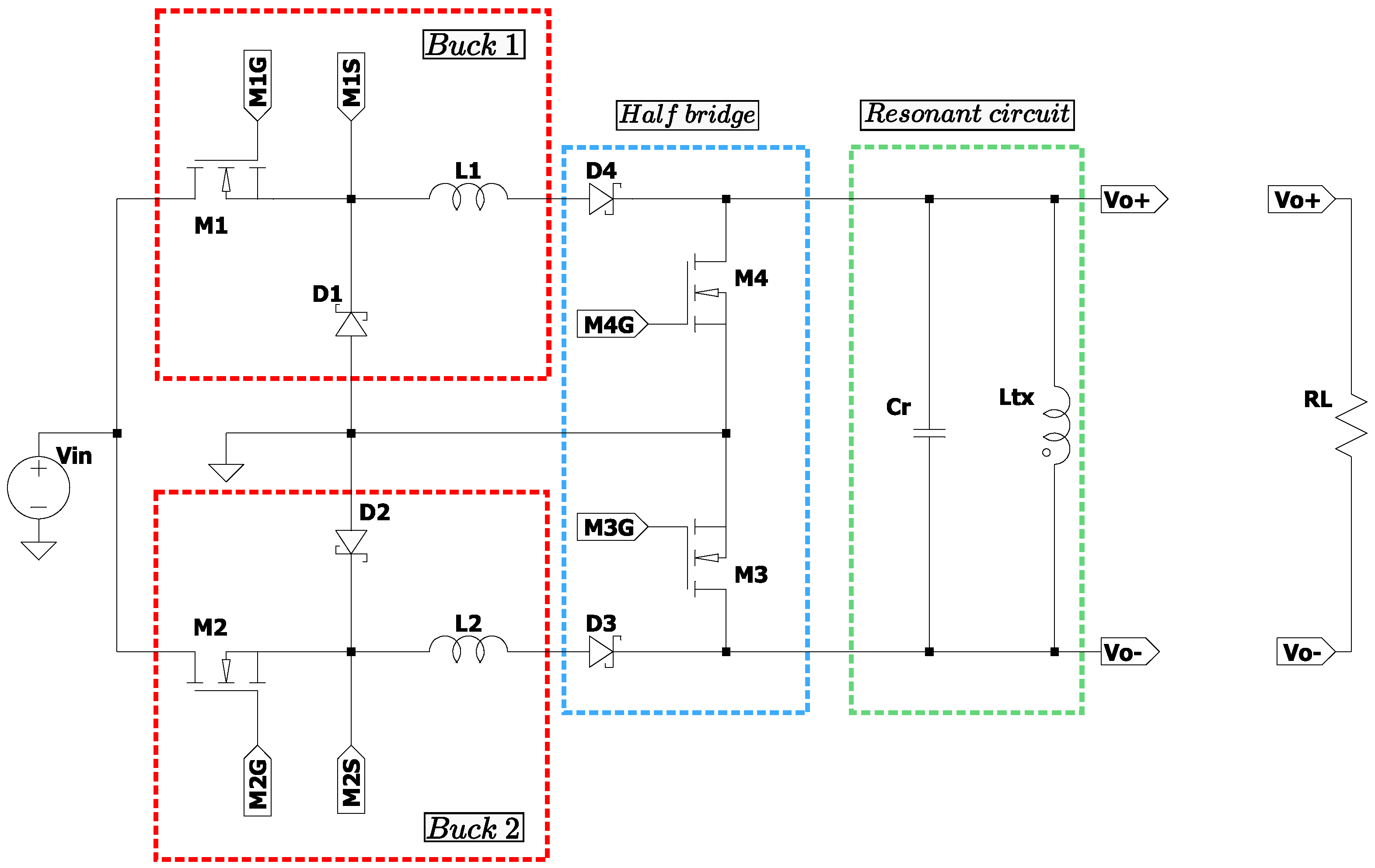
The converter to be controlled is shown in Figure 1. It has been previously analyzed in [16]; however, neither a precise modeling process nor a control strategy has been proposed for this converter.
Constituent parts of the converter are highlighted in the Figure 1. Two bucks converters are clearly distinguished; the first one is formed by MOSFET-diode pair and inductor ; the second buck is formed by the pair and inductor . Both buck converters drive a half-bridge inverter formed by and MOSFET-diode pairs. The parallel resonant stage is formed by capacitor and inductor . Finally, an unknown load is used to model the receptor side.
Qualitatively, the converter can be described as follows. MOSFET-diode pairs and create currents and . From these currents, using and pairs, a square current pulse is injected at the parallel resonant tank. The tank will filter out most of the non-resonant frequencies and produce a nearly sinusoidal output voltage of frequency equal to the filter resonant frequency. The peak value of this output voltage is proportional to (the average value of) and .
To obtain a precise model of the converter it is convenient to distinguish two operation modes; one that produces the positive part of the sinusoidal output voltage and one that produces the negative part. These modes are activated alternately by complementary commutation signals and that switch and MOSFETs, respectively, (see Figure 2). These modes are explained below.
- Mode 1
- In this mode, control signals are as follows: ; and switches on and off. That is, and are off. is ON and is turned on and off continuously in this mode. Hence, the converter behaves as shown in Figure 3. The two possible paths for current in this mode are shown in Figure 3. The actual current path depends on whether is on or off (see Figure 2). As can be observed there is a current at the input of the resonant tank. The average amplitude of such current can be controlled by the duty cycle of MOSFET using the control signal .
- Mode 2
- In this mode control signals are as follows ; and switches on and off. Therefore, in this mode and are off. is on and is turned on and off continuously. Under such circumstances, the converter behaves as shown in Figure 4. Possible paths for current are also shown in the Figure. The actual current path depends on whether is on or off (see Figure 2). Note, that like the Mode 1, in this mode, a current is injected into the resonant tank; however, the direction of such current is the opposite of Mode 1. The average amplitude of the current injected into the resonant tank in this mode can be controlled by switching the MOSFET using the control signal .
The modes described above work alternately. Consequently, a square current is formed at the input of the parallel resonant stage composed of capacitor and inductor . The frequency of such a current is the same frequency of or . The tank must be designed to resonate at this frequency; when this happens, the converter output is near the sinusoidal voltage of this frequency denoted by (see Figure 2).
As has been outlined, the converter generates an AC current from a DC current. The amplitude of the output voltage depends on the amplitude of the square current at the resonant tank which depends on the average of the and currents. Consequently, the output voltage is proportional to the average of and currents. These currents can be controlled by the duty cycle of and that is and , respectively. Note, that for , to control the average of , their frequency, denoted by , must be higher than , . Summing up, with an appropriate control strategy the output voltage can be controlled with the duty cycles and .
Below, a model of the converter of Figure 1 is developed and then a model-based control strategy is proposed.
3. Modeling and Open-Loop Simulation
To build a manageable model for control design purposes, it is necessary to make some simplifications. Two assumptions are commonly made in power converter modeling
- Consider MOSFET-diode pairs as ideal switches.
- Consider ideal electronics components.
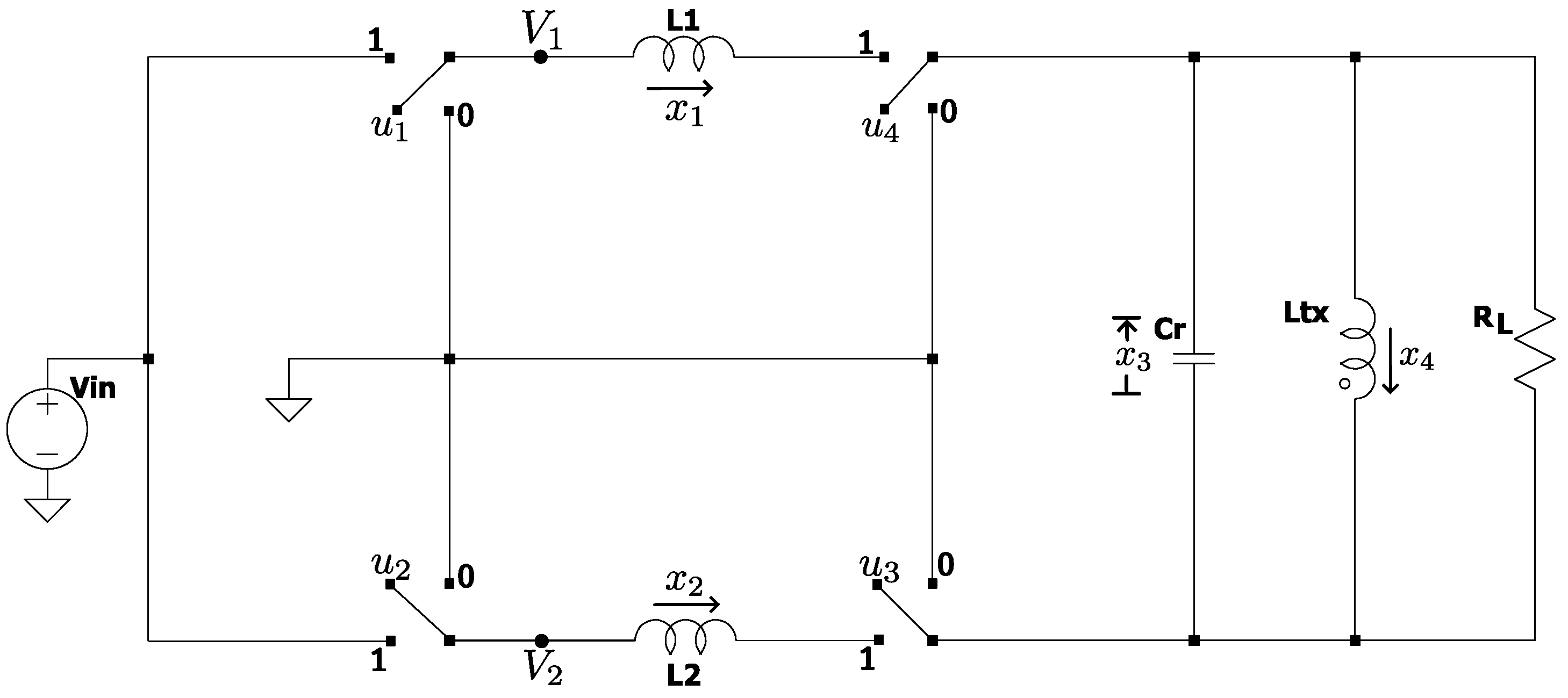
With such assumptions the converter simplified diagram depicted in Figure 5 is obtained. As observed in the Figure, the following notation common in control theory is used
- denote
- denote
- denote
- denote
Furthermore, denotes the output current. To simplify the model derivation, it will be first supposed that voltages and indicated in Figure 5 are known. Such an assumption will be eliminated later. Converter behavior is different for the two modes. Therefore, it is necessary to obtain a model for each one.
Model of Mode 1: . In this case the converter is described by
Model of Mode 2: . In this case the converter equations become
Combining models (1) and (2) into a single set of equations, results in
Taking into account,
substituting (4) in (3) and leaving only the state variables on the left side, results in
Expressions (5) is a switched nonlinear model of converter shown in Figure 1.
The converter design procedure can be divided into two steps:
- design the resonant stage
- design inductors ( and ) of the buck converters.
Both steps are independent.
To design the resonant stage, the relation between the resonant frequency (in hertz), inductor and capacitor
must be taken into account. If a is selected, appropriate values for inductor and capacitor can be chosen. In this work, a resonant frequency of about 100 KHz was selected. Since the inductor is a crucial analog component of the converter, a commercial inductor (Würth electronics 76030811) with H was chosen. From such frequency and inductance, using (6) capacitor value results in F.
Buck converter design, and hence the calculation of its inductor value, is described in power electronics books, for example, [18]. Following such guidelines, H was obtained. The converter parameter values obtained are summarized in Table 1.
To be confident that model (5) properly describes the converter, it was simulated and compared against a simulation obtained using an LTspice component-model-based simulator. LTspice uses a model for each electronic component.
The simulation of model (5) is straightforward. One of many dynamical systems simulation software can be used. For example, XPPAut [19]. However, for LTspice component-based simulation it is necessary to provide additional details.
The converter was simulated using the components listed in Table 1. As explained above, and are complementary pulses with a duty cycle of and a switching frequency of . The signal to switch MOSFET is produced with a pulse voltage source; the same signal passed through an inverted provides the switching signal for (see Figure 6). From and the PWM pulses for and can be obtained. However, since only switches when is on, the switching signal of is ANDed with pulse. Similarly, the switching signal of is ANDed with pulse. Having switching signals for all MOSFETs, voltage-controlled sources are used to amplify such signals and obtain gate voltage for each MOSFETs (see Figure 6). All this logic is encapsulated as shown in Figure 6. From now on, this block is used to simplify the gate voltage generation from and .
Note, that in Figure 6 there are two PWM blocks. The implementation of these two blocks is depicted in Figure 7. As can be observed, PWM consists of a pulsating source (Osc), a Saw-tooth source (Swt), a comparator and SR flip-flop. The pulse and sawtooth sources have a frequency of , pulse has a duty cycle of 1%. PWM operation is as follows: the flip-flop is set using the pulse at the beginning of each commutation cycle. When SwT equals d, the comparator resets the flip-flop. Consequently, the PWM output is a pulse of frequency and duty cycle d. Although commercial PWM blocks and drives could be used, it is worth noting that this paper aims to present a feasible control strategy to be implemented using an ad-hoc integrated circuit, not with discrete components.
Having the drive that processes duty cycles and to generate the MOSFET gate signals, open-loop LTspice simulation is easy to perform. It is only necessary to include the drive block in the converter of Figure 1.
Figure 8 shows a comparison of the output voltage in XPPAut and LTspice. It can be observed that both environments produce qualitatively similar results. However, LTspice simulation yields an output with a noticeably smaller amplitude. This is due to the model (5) ideal components being considered while LTspice has a more precise model for each device; particularly, LTspice takes into account voltage drop in switching devices, time to switch on and off and parasite elements in capacitors and inductors, etc.
In what follows, model (5) is used to derive the control strategy; however, for simulations to be closer to real results, henceforth, simulations will be performed in LTspice.
Before presenting the proposed control strategy, it is convenient to show that without compensation the converter is very sensitive to load and input voltage variations. Figure 9 was obtained when the load changes, from 80 to 10 at S. It can be observed that when the load changes, the output voltage changes significantly.
A second open loop simulation is shown in Figure 10. In this simulation, the load has a constant value of 10 ; the input voltage changes from 15 V to 20 V at 150 S. It can be observed from this figure that the output voltage is very sensitive to input voltage variations.
4. Control Strategy Derivation
For a better explanation of the proposed control, it is convenient to rewrite model (5) to clearly distinguish the two main subsystems of the converter: (a) the two buck converters and the half-bridge that produce a square current of variable amplitude and (b) the resonant stage. To this end, let be the current flowing into the resonant tank. This current is given by
Using (7), model (5) can be written as
The converter’s inner workings can be better understood from the model (7,8) because two converter subsystems can be identified. The subsystem described by (8a, 8b) generates given by (7). Then, is injected into the resonant subsystem described by (8c, 8d) to produce the output voltage . From this observation, the following general control ideas can be derived:
- First, determine the necessary current that must flow into the resonant tank. Denote such current as .
- Having , determine the current that inductors and must have. That is, determine the references for and . Denote these references as and .
- Have and determine the duty cycle of and to achieve and , where and are the average current of and , respectively.
Below it is described how to carry out each of these steps.
Determine the necessary current that must flow into the resonant tank:
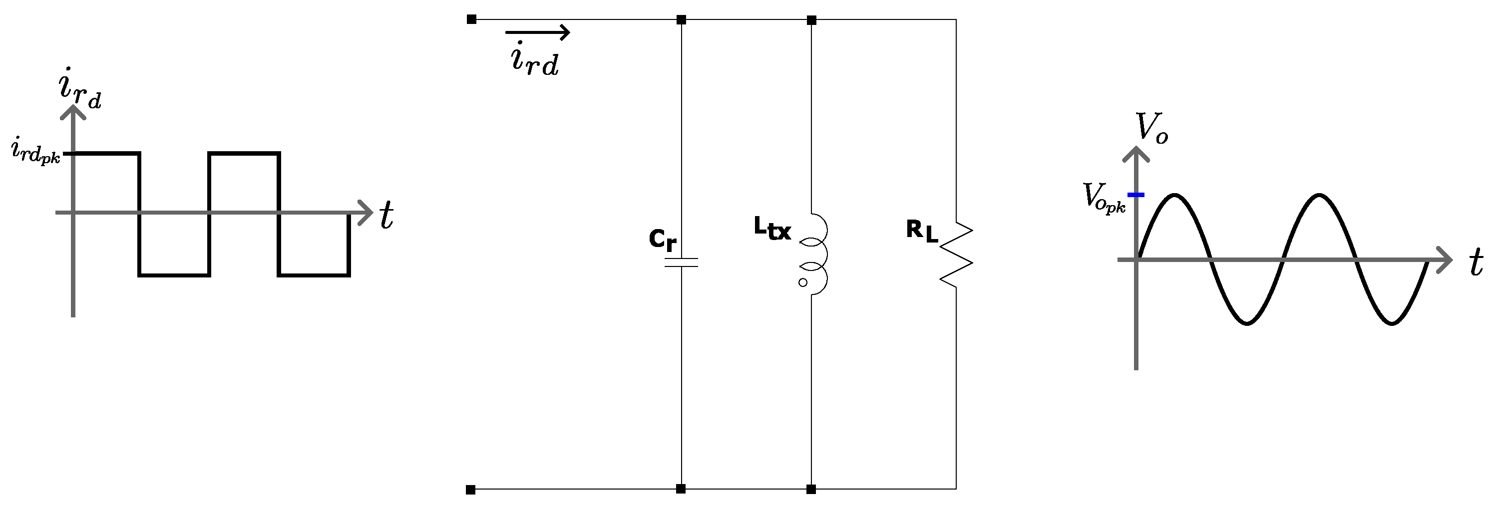
Expressions (8c, 8d) correspond to a parallel RLC resonant converter with as input source. Hence, must be (a) a periodic signal with a fundamental frequency equal to the resonant frequency and (b) its amplitude () must be such that the peak output voltage () have the desired value (see Figure 11).
As has been outlined above from (7), we precisely observed that to achieve the required frequency, and must be complementary pulses of the same frequency as the resonant frequency of the converter. Therefore, it is only necessary to determine the peak value of that is .
The current peak depends on the load. However, the load is unknown; hence, the value of should be dynamically estimated. Here, it is proposed that
where
with as the desired output peak voltage and as the real output peak voltage. It is important to point out that expressions (9, 10) adjust the (desired) amplitude of current that flows into the resonant tank.
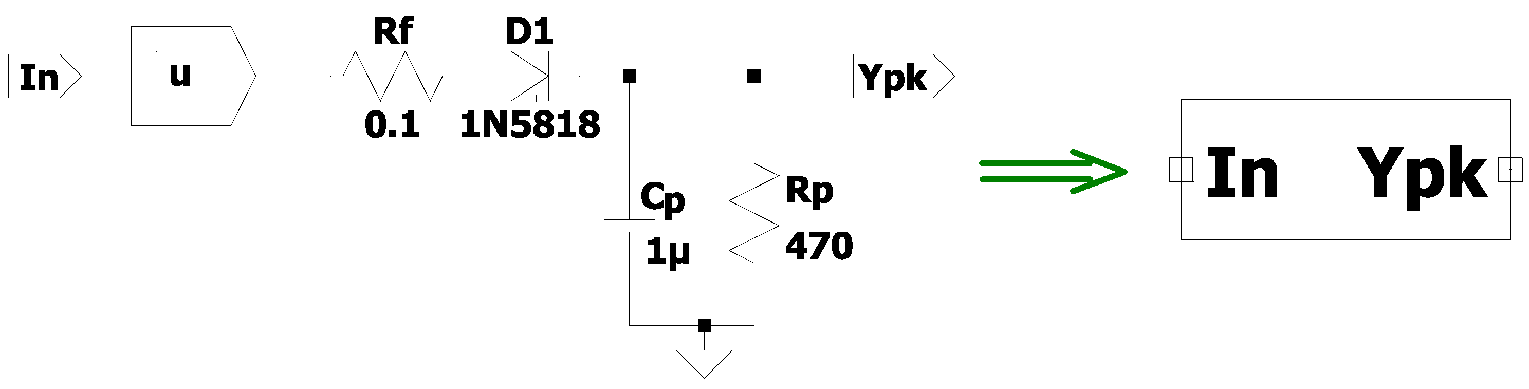
Observe that to implement (9) it is necessary to know the peak output voltage . There are several ways to measure the peak of a sinusoidal voltage. One way is with the subcircuit shown in Figure 12. Mathematically, Figure 12 can be modeled as
Having the converter peak output voltage expressions (9, 10) can now be implemented; consequently, the desired input to the resonant part is known.
Determination of reference and
Current is obtained by the sum of inductor currents and ; more precisely forms the positive semicycle of and forms the negative semicycle; both have the same magnitude. Therefore, references and for inductor currents are equal and given by
Determination of duty cycle of and
To achieve
where and are the average of and , respectively. To obtain the duty cycle of and the average of expressions (8a, 8b) must be used. That is
where , , and are the duty cycle of , , and , respectively. Note, that
From (14) it can be observed that control laws
guarantee (13); this can be verified by substituting (15) in (14) which yields
From (16), it can be observed that (13) is indeed guaranteed.
Expressions (15) can be simplified by observing that changes significantly slower than the change of and . Therefore, can be dropped off from (15). Thus, duty cycles become
Duty cycle expressions (17) can be further simplified. Since and are adjusted dynamically (see expression (12) and (9)), division by in (17) is unnecessary because any error would be compensated by the integral term in (9). Therefore, duty cycle expressions finally become
Summing up, the proposed controller is given by (9, 10, 11, 12 and 18). More precisely, (18) provides and duty cycles; (12) express that the references for currents and are equal to (peak value of) the current that must flow into the resonant tank; this current is given by (9) and (10). Finally, the peak output voltage necessary in (10) is calculated by (11). The controller given by these expressions can, in fact, be easily implemented with electronic components as shown in Figure 13. The drive block and PkDetect block appearing in this figure are detailed in Figure 6 and Figure 12 respectively.
To simplify the controller simulation in LTspice, some blocks of the educational library [20] were used. Each of these blocks, and hence the complete controller, can be implemented using discrete components; however, as has been mentioned, the strategy presented here is intended to be implemented with an ad-hoc integrated circuit.
5. Simulation Results
It is worth noting that the only controller parameters are and of expression (9). The relation between the current at the resonant stage and the output error depends on the (unknown) load and is nonlinear. Hence, the root-locus [21] method cannot be used. Instead, Zieglers–Nichols [22] or heuristic optimization methods like particle swarm optimization [23] or gray wolf optimization [24] can be used.
The Ziegler–Nichols method [22] consists of two heuristic procedures, one is applicable to systems closed-loop systems that can not be operated in an open loop and the other is to design feedback for open-loop systems. The procedure for closed-loop firstly eliminates the integral term and increases the proportional gain until sustained oscillations are produced. The that produces such oscillations and its period are used to obtain the controller gains. The procedure for the open loop introduces a step input to the system. From the system response the time delay of the response, its slope and the stationary state are used to obtain the controller gains. The Ziegler–Nichols method is a long-standing proven method for controller tunning; it is simple and requires very little system information. However, the procedure for closed-loop is time-consuming and takes the system near to instability region which can be dangerous for some systems; open-loop procedure can yield wrong controller gains, particularly for nonlinear systems. In both cases controller parameters provided by the Zieglers–Nichols method usually have to be fine-adjusted to improve closed-loop performance.
Swarm intelligence optimization algorithms, like Particle Swarm Optimization [23] (PSO) and Gray Wolf Optimization [24] (GWO) requires a model and makes use of intensive simulations. These algorithms consider controller parameters as the coordinates of a point in a space called solution space. Hence, each point in the solution space is associated with a particular controller. Swarm algorithms start with a set of randomly generated controllers (also called points or solutions). Each controller is simulated and depending on its performance a fitness is assigned to each controller. Using each controller’s fitness and evolution rules, a second set of controllers is generated; then a third and so on. Evolution rules to obtain a new generation of controllers are inspired by nature, particularly on the behavior of animals living in groups. Generally, evolution rules make that for each generation, solutions move closer to the best-known solutions of previous generations but with random components aimed to explore new places of the solution space. Algorithms of this kind usually end when a predetermined number of iterations has been reached or when no better solution can be obtained. The optimum solution is the best solution of the last generation. Swarm intelligence algorithms are offline methods that always require a model and convergence to the optimum can not be guaranteed; however, they have been successfully applied to a great variety of nonlinear problems [25]. Furthermore, perturbations can be taken into account in the evolution of these algorithms. For such reasons, in this work, it was decided to use the gray wolf optimization algorithm. Using this method for the converter of Figure 1 compensated by the controller of Figure 13 the parameters values: and were obtained.
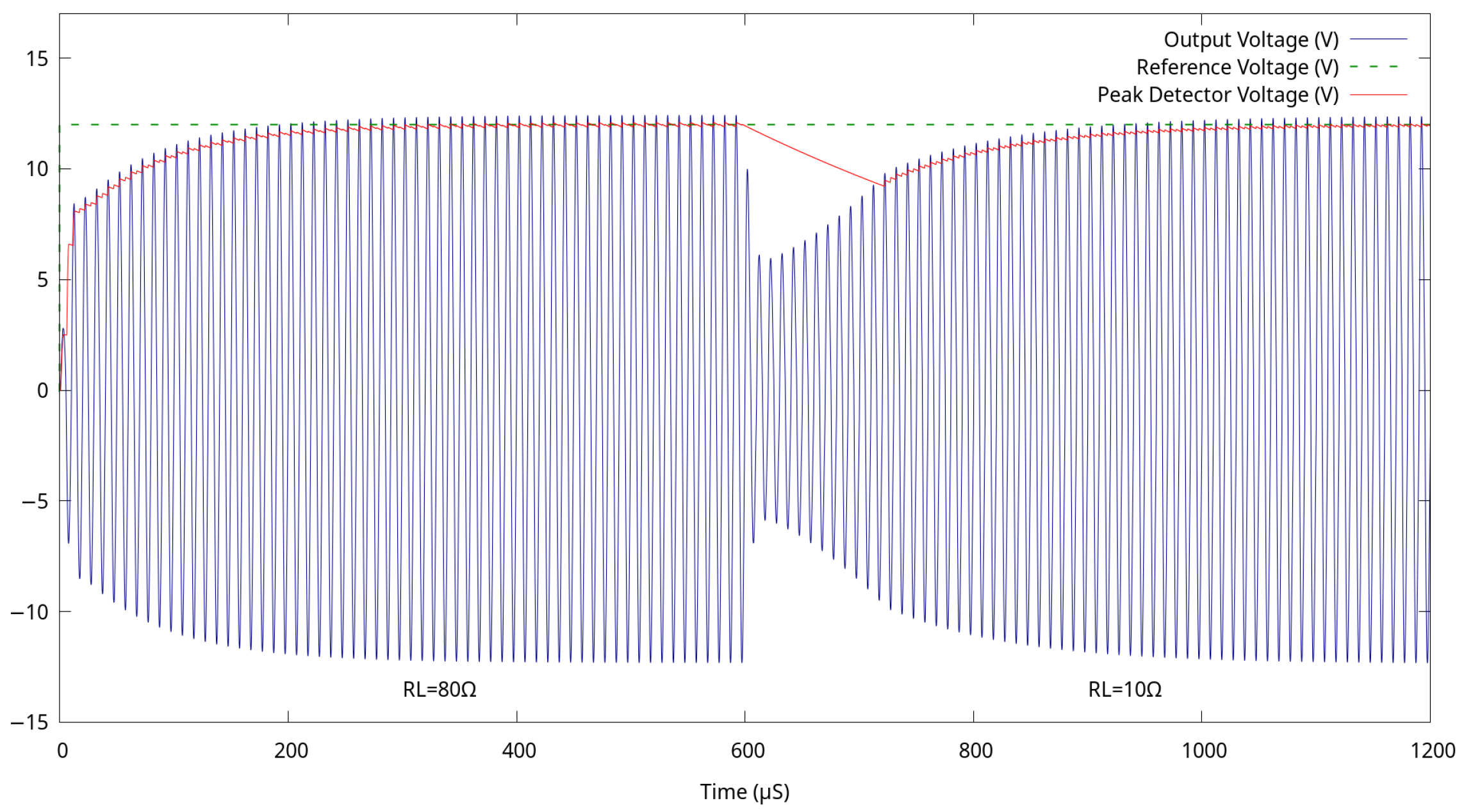
Figure 14 shows a closed-loop performance under the load variation of the compensated converter. The Figure shows the output voltage (), the measured peak output voltage () and the desired peak output voltage (). At the beginning the load is 80 ; at S the load is suddenly changed to 10 . As can be observed the controller compensates for the change within S.
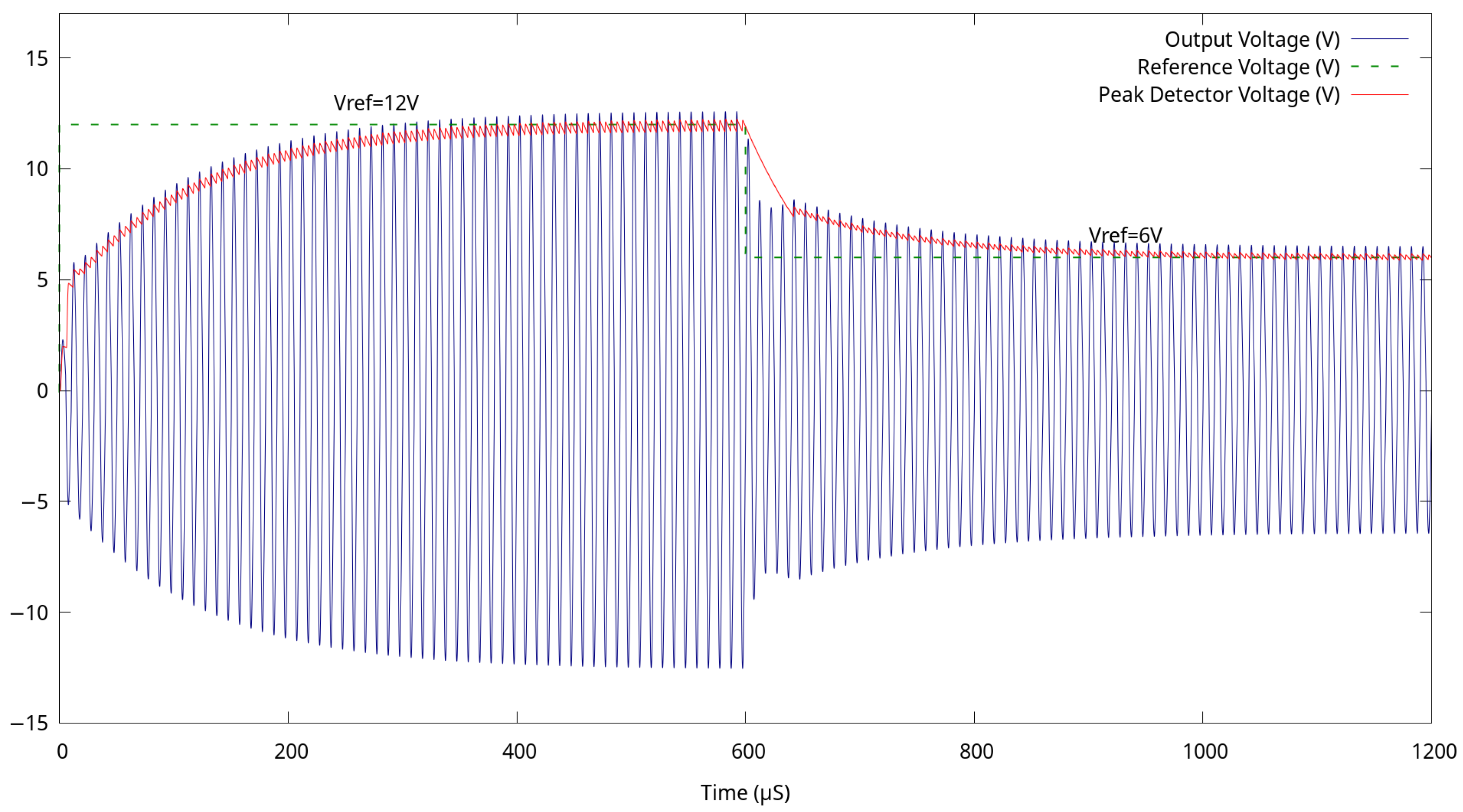
To show the performance of the compensated converter when the reference changes a simulation was carried out. The results are shown in Figure 15. At the beginning of this simulation, the reference for the peak output voltage () is 12 V; note, that the controller reaches the stationary state within S. At S the reference is changed to 6 V; it can be observed the controller compensates the change within S.
A third closed-loop simulation to show the performance of the controlled converter under input voltage variation was carried out. The result is shown in Figure 16. At the start of this simulation, the input voltage is 15 V; then at S, is changed to 20 V. It can be observed that the influence of an input voltage change on the output voltage is small and it is compensated very quickly (within S).
Remark 1.
From decades now it has been known that for DC/DC converters (like buck or boost), instead of directly control the output voltage with a PI control is preferable to control the inductor current and through this indirectly control the output voltage [26]. This idea, sometimes has been called indirect control [27,28]. To apply this idea a reference for the inductor current is needed. Usually, this reference is constructed with a PI estimator. Although we not look for the application of indirect control to the inductive wireless power transmitter the obtained controller directly modify the inductors currents and then indirectly control, via a peak detector and a PI, the output voltage. That is the proposed controller resembles the indirect control.
Remark 2.
Indirect control explain why the compensation of input voltage variation is much faster than to compensate load or reference variations. Reference variation and load variation has an effect on the output error. Such error will be reflected in the inductors currents references, through the peak detector and the PI estimator. However, the peak detector as well as the PI estimator are dynamical, both dynamics slow down the reflection of the output error on the inductors current references. On the contrary an input voltage variation directly affects inductor currents and ; both current are directly compensated by the controller.
Compensation times between load variation and reference variation are explained by the magnitude of the change on the output voltage when the perturbation is introduced. When the load change the output voltage drop from 12 V to 5.5 V; from this value the output voltage has to be recovered to 12 V. When the reference is changed the output voltage drop from 12 V to 8 V and from this point the objective of 6 V has to be reached.
A comparison between the proposed topology and its modeling control strategy with recent WPT systems proposed recently is presented in Table 2.
6. Conclusions
In this work, a model and a control strategy for a previously proposed converter to be used in inductive wireless power transmission have been proposed. The converter is composed of two buck converters and a half-bridge that feeds a resonant stage. For this converter, a nonlinear switched model has been built step by step. Using such a model, a controller was derived without relying on system linearization. Although the resulting controller is strongly nonlinear it is also surprisingly simple and easy to implement. Despite its simplicity, the controller makes the compensated converter very fast and robust under load variation, input voltage variations and changes on its reference.
The controller derivation has been explained in detail. The necessary input current that must be fed into the resonant stage is determined using a PI control over the error on the peak voltage; then a the proportional controller on each buck converter attains the necessary current into the resonant stage. The overall scheme is robust and suitable for a great variety of applications.
The control strategy employed in this paper can also be used as a start point to control other resonant-tank-based wireless power transfer systems.
Author Contributions
Conceptualization, D.C. and L.H.-G.; methodology, D.C., L.H.-G. and J.R.-H.; software, D.C., L.H.-G. and M.V.; validation, J.R.-H., M.V. and L.H.-G.; formal analysis, D.C. and J.R.-H.; investigation, D.C. and L.H.-G.; resources, D.C. and L.H.-G.; data curation, J.R.-H. and M.V.; writing—original draft preparation, D.C. and L.H.-G.; writing—review and editing, J.R.-H. and M.V.; visualization, D.C. and M.V.; supervision, D.C. and L.H.-G.; project administration, J.R.-H. and M.V.; funding acquisition, D.C. and L.H.-G. All authors have read and agreed to the published version of the manuscript.
Funding
This research was funded by Instituto Politécnico Nacional of Mexico and CONAHCYT of Mexico.
Data Availability Statement
All the necessary information to reproduce the results of this paper is self contained. In case of further information is required please contact the first author.
Conflicts of Interest
The authors declare no conflict of interest.
Abbreviations
The following abbreviations are used in this manuscript:
| IWPT | Inductive wireless power transfer |
| WPT | Wireless power transfer |
| Resonant frequency | |
| Desired current reference | |
| Peak output current | |
| Peak output voltage | |
| Desired peak output voltage | |
| Desired peak current reference |
References
- Cai, C.; Saeedifard, M.; Wang, J.; Zhang, P.; Zhao, J.; Hong, Y. A Cost-Effective Segmented Dynamic Wireless Charging System with Stable Efficiency and Output Power. IEEE Trans. Power Electron. 2022, 37, 8682–8700. [Google Scholar] [CrossRef]
- Xiong, H.; Xiang, B.; Mao, Y. An Auxiliary Passive Circuit and Control Design for Wireless Power Transfer Systems in DC Microgrids with Zero Voltage Switching and Accurate Output Regulations. Energies 2023, 16, 694. [Google Scholar] [CrossRef]
- Kabbara, W.; Bensetti, M.; Phulpin, T.; Caillierez, A.; Loudot, S.; Sadarnac, D. A Control Strategy to Avoid Drop and Inrush Currents during Transient Phases in a Multi-Transmitters DIPT System. Energies 2022, 15, 2911. [Google Scholar] [CrossRef]
- Chen, X.; Gong, X. Modeling of wireless power system with giant magnetostrictive material load under multi-field coupling. In Proceedings of the Conference Proceedings—IEEE Applied Power Electronics Conference and Exposition—APEC, Tampa, FL, USA, 26–30 March 2017; pp. 3100–3105. [Google Scholar]
- Nagashima, T.; Wei, X.; Bou, E.; Alarcón, E.; Kazimierczuk, M.K.; Sekiya, H. Analysis and Design of Loosely Inductive Coupled Wireless Power Transfer System Based on Class-E2 DC-DC Converter for Efficiency Enhancement. IEEE Trans. Circuits Syst. Regul. Pap. 2015, 62, 2781–2791. [Google Scholar] [CrossRef]
- Mai, R.; Ma, L.; Liu, Y.; Yue, P.; Cao, G.; He, Z. A Maximum Efficiency Point Tracking Control Scheme Based on Different Cross Coupling of Dual-Receiver Inductive Power Transfer System. Energies 2017, 10, 217. [Google Scholar] [CrossRef]
- Li, B.; Geng, Y.; Lin, F.; Yang, Z.; Igarashi, S. Design of constant voltage compensation topology applied to wpt system for electrical vehicles. In Proceedings of the 2016 IEEE Vehicle Power and Propulsion Conference (VPPC), Hangzhou, China, 17–20 October 2016; pp. 1–6. [Google Scholar]
- RamRakhyani, A.K.; Mirabbasi, S.; Chiao, M. Design and optimization of resonance-based efficient wireless power delivery systems for biomedical implants. IEEE Trans. Biomed. Circuits Syst. 2010, 5, 48–63. [Google Scholar] [CrossRef] [PubMed]
- Xue, R.F.; Cheng, K.W.; Je, M. High-Efficiency Wireless Power Transfer for Biomedical Implants by Optimal Resonant Load Transformation. IEEE Trans. Circuits Syst. Regul. Pap. 2013, 60, 867–874. [Google Scholar] [CrossRef]
- Shin, J.; Shin, S.; Kim, Y.; Ahn, S.; Lee, S.; Jung, G.; Jeon, S.J.; Cho, D.H. Design and implementation of shaped magnetic-resonance-based wireless power transfer system for roadway-powered moving electric vehicles. IEEE Trans. Ind. Electron. 2013, 61, 1179–1192. [Google Scholar] [CrossRef]
- Huh, J.; Lee, S.W.; Lee, W.Y.; Cho, G.H.; Rim, C.T. Narrow-width inductive power transfer system for online electrical vehicles. IEEE Trans. Power Electron. 2011, 26, 3666–3679. [Google Scholar] [CrossRef]
- Madawala, U. A Bidirectional Inductive Power Interface for Electric Vehicles in V2G System. IEEE Trans. Ind. Electron. 2010, 58, 2789–2796. [Google Scholar] [CrossRef]
- Hoang, H.; Lee, S.; Kim, Y.; Choi, Y.; Bien, F. An adaptive technique to improve wireless power transfer for consumer electronics. IEEE Trans. Consum. Electron. 2012, 58, 327–332. [Google Scholar] [CrossRef]
- Lin, J.C. Wireless power transfer for mobile applications, and health effects [telecommunications health and safety]. IEEE Antennas Propag. Mag. 2013, 55, 250–253. [Google Scholar] [CrossRef]
- Lu, X.; Niyato, D.; Wang, P.; Kim, D.I.; Han, Z. Wireless charger networking for mobile devices: Fundamentals, standards, and applications. IEEE Wirel. Commun. 2015, 22, 126–135. [Google Scholar] [CrossRef]
- Carbajal-Retana, M.; Hernandez-Gonzalez, L.; Ramirez-Hernandez, J.; Avalos-Ochoa, J.G.; Guevara-Lopez, P.; Loboda, I.; Sotres-Jara, L.A. Interleaved buck converter for inductive wireless power transfer in DC–DC converters. Electronics 2020, 9, 949. [Google Scholar] [CrossRef]
- Cortes, D.; Alvarez, J.; Álvarez, J.; Fradkov, A. Tracking control of the boost converter. IEE-Proc.-Control. Theory Appl. 2004, 151, 218–224. [Google Scholar] [CrossRef]
- Erickson, R.W.; Maksimovic, D. Fundamentals of Power Electronics; Springer Science & Business Media: Berlin/Heidelberg, Germany, 2007. [Google Scholar]
- Ermentrout, B. Simulating, Analyzing, and Animating Dynamical Systems: A Guide Toi Xppaut for Researchers and Students; Society for Industrial and Applied Mathematics: Philadelphia, PA, USA, 2002. [Google Scholar]
- Alonso, J.M. Simulink-Compatible Control Library for LTspice. 2023. Available online: https://sites.google.com/view/j-marcos-alonso/home (accessed on 20 March 2024).
- Šekara, T.B.; Rapaić, M.R. A revision of root locus method with applications. J. Process. Control. 2015, 34, 26–34. [Google Scholar] [CrossRef]
- Åström, K.J.; Hägglund, T. Revisiting the Ziegler–Nichols step response method for PID control. J. Process. Control. 2004, 14, 635–650. [Google Scholar] [CrossRef]
- Eberhart, R.; Kennedy, J. Particle swarm optimization. In Proceedings of the IEEE International Conference on Neural Networks, Citeseer, Perth, WA, Australia, 27 November–1 December 1995; Volume 4, pp. 1942–1948. [Google Scholar]
- Mirjalili, S.; Mirjalili, S.M.; Lewis, A. Grey wolf optimizer. Adv. Eng. Softw. 2014, 69, 46–61. [Google Scholar] [CrossRef]
- Wang, X.; Xiao, J. PSO-Based Model Predictive Control for Nonlinear Processes. In Proceedings of the Advances in Natural Computation; Wang, L., Chen, K., Ong, Y.S., Eds.; Springer: Berlin/Heidelberg, Germany, 2005; pp. 196–203. [Google Scholar]
- Middlebrook, R. Modeling current-programmed buck and boost regulators. IEEE Trans. Power Electron. 1989, 4, 36–52. [Google Scholar] [CrossRef]
- Alvarez, J.; Cortes, D.; Alvarez, J. Indirect control of high frequency power converters for AC generation. In Proceedings of the 39th IEEE Conference on Decision and Control (Cat. No.00CH37187), Sydney, NSW, Australia, 12–15 December 2000; Volume 4, pp. 4072–4077. [Google Scholar] [CrossRef]
- Tan, S.C.; Lai, Y.M.; Tse, C.K. Indirect Sliding Mode Control of Power Converters Via Double Integral Sliding Surface. IEEE Trans. Power Electron. 2008, 23, 600–611. [Google Scholar] [CrossRef]
Figure 1.
Inductive Wireless Power Transmitter to be controlled.

Figure 2.
Converter switching signals.

Figure 3.
Converter behavior in mode 1.

Figure 4.
Converter behavior in mode 2.

Figure 5.
Converter simplified diagram with ideal switches.

Figure 6.
Drive for MOSFETs .

Figure 7.
PWM block.

Figure 8.
Output voltage obtained using LTspice model of Figure 1.
Figure 8.
Output voltage obtained using LTspice model of Figure 1.

Figure 9.
Open-loop performance under load variation.

Figure 10.
Open-loop performance under input voltage variation.

Figure 11.
Current input and voltage output of resonant stage.

Figure 12.
Measuring the peak voltage.

Figure 13.
Controller implementation.

Figure 14.
Closed loop performance under load variation.

Figure 15.
Closed loop performance under reference variation.

Figure 16.
Closed loop performance under input voltage variation.


Table 1.
Converter components and parameters.
| CMF10120D | |
| 1N5822 | |
| 1 MHz | |
| 100 KHz | |
| 0.4 | |
| 76030811 -Würth (, ) | |
| Q | 80 |
Table 2.
Comparison among recently proposed WPT systems.
| Topology Factor | Proposed Modeling and Control IPT | Control Design for Wireless Power Transfer [2] | A Control Strategy to Avoid Drop and Inrush Currents [3] | A Maximum Efficiency Point Tracking Control Scheme [6] | A Cost-Effective Segmented Dynamic Wireless Charging [1] |
|---|---|---|---|---|---|
| Application | Battery charge | DC Microgrids | Charging EVs | Wireless power supply for locomotives | Dynamic charging |
| Control circuit | Peak meter + PI | PI + Phase Shift | PID | PI | — |
| Switching frequency | 500 kHz | 100 kHz | 15 kHz | 20.3 kHz | 150 kHz |
| Efficiency | 85.1% | 80% | — | 84% | 87% |
| Output Power | 15 W | 540 mW | 700 W | 2 kW | 192 W |
| Advantages | The topology and control method are simple and achieve high efficiency | Proposes an auxiliary method to help the switches in the full-bridge inverter achieve soft switching | Presents a novel control strategy for multi-transmitter DIPT systems that ensures a continuous and stable power transfer | Proposed a method to track the maximum efficiency point for against the variation of the load | Proposed a Costed-Effective DWPT system for dynamic charging of autonomous moving equipment with stable performance |
| Major Drawbacks | Work in progress to achieve higher output power | Not recommended for heavy load conditions | The achieved efficiency is not reported, the operating frequency is below the standard | Five measurements and three controllers are required | Detection of the position of the Rx is necessary to switch the Tx coil segments ON or OFF |
Disclaimer/Publisher’s Note: The statements, opinions and data contained in all publications are solely those of the individual author(s) and contributor(s) and not of MDPI and/or the editor(s). MDPI and/or the editor(s) disclaim responsibility for any injury to people or property resulting from any ideas, methods, instructions or products referred to in the content. |
© 2024 by the authors. Licensee MDPI, Basel, Switzerland. This article is an open access article distributed under the terms and conditions of the Creative Commons Attribution (CC BY) license (https://creativecommons.org/licenses/by/4.0/).
Share and Cite
MDPI and ACS Style
Cortes, D.; Hernandez-Gonzalez, L.; Ramirez-Hernandez, J.; Vargas, M. Modeling and Control of an Inductive Power Transmitter Based on Buck–Half Bridge–Resonant Tank. Electronics 2024, 13, 1593. https://doi.org/10.3390/electronics13081593
AMA Style
Cortes D, Hernandez-Gonzalez L, Ramirez-Hernandez J, Vargas M. Modeling and Control of an Inductive Power Transmitter Based on Buck–Half Bridge–Resonant Tank. Electronics. 2024; 13(8):1593. https://doi.org/10.3390/electronics13081593
Chicago/Turabian StyleCortes, Domingo, Leobardo Hernandez-Gonzalez, Jazmin Ramirez-Hernandez, and Maria Vargas. 2024. "Modeling and Control of an Inductive Power Transmitter Based on Buck–Half Bridge–Resonant Tank" Electronics 13, no. 8: 1593. https://doi.org/10.3390/electronics13081593
Note that from the first issue of 2016, this journal uses article numbers instead of page numbers. See further details here.