Article

Constant-Voltage and Constant-Current Controls of the Inductive Power Transfer System for Electric Vehicles Based on Full-Bridge Synchronous Rectification

1
School of Electrical Engineering, Naval University of Engineering, Wuhan 430000, China
2
National Key Laboratory of Electromagnetic Energy, Naval University of Engineering, Wuhan 430000, China
*
Authors to whom correspondence should be addressed.
Electronics 2024, 13(9), 1686; https://doi.org/10.3390/electronics13091686
Submission received: 30 March 2024 / Revised: 22 April 2024 / Accepted: 25 April 2024 / Published: 26 April 2024

Abstract

:
When an inductive power transfer (IPT) system conducts wireless charging for electric cars, the coupling coefficient between the coils is easily affected by fluctuations in the external environment. With frequent changes in the battery load impedance, it is difficult for the IPT system to achieve constant-voltage and constant-current (CVCC) controls. A CVCC control method is proposed for the IPT system that has a double-sided LCC compensation structure based on full-bridge synchronous rectification. The proposed method achieved good dynamic stability and was able to effectively switch between the output current and voltage of the system by adjusting only the duty cycle of the switch on the secondary side of the rectification bridge. As a result, the system efficiency was improved. The output characteristics of the double-sided LCC compensation structure was derived and the conduction condition with zero voltage was analyzed by using four switches through two conduction time series of the rectifier circuit. Then, the output voltage of the synchronized rectifier was derived. The hardware implementation of the full-bridge controllable rectifier was described in detail. Finally, a MATLAB/Simulink 2018a simulation model was developed and applied to an 11 kW prototype to analyze and validate the design. The results showed that the designed system had good CVCC output characteristics and could maintain constant output under certain coupling offsets. Compared with semi synchronous rectification methods, the proposed method had a higher efficiency, which was 95.6% at the rated load.

1. Introduction

In recent years, with the development of the economy and advancements in technology, electricity has been fully developed and utilized as a high-quality energy source. However, optimizing the method of electricity conversion and improving its efficiency remain pressing issues [1,2]. Inductive power transfer (IPT) technology has been widely employed in electrical energy transmission without the need for electrical hardware connections at both the power supply and receiving sides. It is known for its flexibility, convenience, safety, and reliability, leading to its rapid development in recent years [3,4,5]. The utilization of IPT technology in electric vehicles facilitates intelligent and convenient charging. With the increasing popularity of plug-in hybrid and electric vehicles, IPT charging solutions have garnered renewed interest [6,7].
When employing the IPT system for charging electric vehicle batteries, it is crucial to consider the charging characteristics. Various charging methods for lithium batteries exist, including constant-current (CC) charging, constant-voltage (CV) charging, and phased constant-voltage constant-current (CVCC) charging [8,9]. Phased CVCC charging is commonly utilized, as depicted in Figure 1.
To realize CC and CV operations of an IPT system, researchers have proposed many methods, mainly including two categories: (1) By designing the parameters of the compensation network, the CC and CV outputs can be realized separately. (2) To realize CC or CV outputs, they can be realized through DC/DC converter, phase shift control and variable frequency control.
In their examination of compensation network parameters, Lu et al. introduce a comprehensive methodology applicable to diverse higher-order resonant circuits [10]. This approach presents an equivalent circuit and a general resonance technique tailored specifically for higher-order resonant circuits, aiming to achieve CC and CV outputs across varying load conditions while preserving zero-phase angle (ZPA) frequencies. Additionally, Ref. [11] outlines a generalized modeling strategy for arbitrary higher-order resonant networks, facilitating the derivation of voltage and current transfer characteristics unaffected by load variations. Such circuits can be conceptualized as combinations of series-connected LC networks, multi-level T circuits, and multi-level Π circuits.
To complete the entire charging process, transitioning from the CC output to the CV output is essential. Once the topological structure is determined, the output characteristics (either CC or CV) are also established. Thus, a method has been proposed to facilitate the switch from CC to CV using a switching topology [12,13]. Previous studies utilized a double-sided LCC (DLCC) compensation structure for the CC charging stage, while the CV charging stage employed a switch to an LCC-S compensation structure. In [14], the transition from CC to CV was accomplished through frequency modulation. This transition occurred at varying operating frequencies by optimizing the parameters of the DLCC compensation structure. Control elements do not have to be added to these methods. Although they are simple and reliable, they cannot handle situations that demand variable output.
However, the relative positions of the coupling coils are not fixed in practical applications, leading to potential changes in the coupling coefficient of the IPT system. For instance, achieving precise alignment of coupling coils during the charging of electric vehicles is challenging, resulting in output fluctuations. In dynamic wireless transmission scenarios like charging unmanned aerial vehicles [15], electric vehicles [16,17], and underwater equipment [18,19], the relative positions of coupling coils continuously change, leading to system output instability. In such applications, stable CV output cannot be attained through switching topology or operating frequency alone. Therefore, specialized control algorithms are necessary to ensure stable output.
The current methods of controlling system power output encompass transmitter-end regulation, receiver-end regulation, and coordinated regulation between the transmitter and receiver ends. In transmitter-end regulation, the methods to adjust the input voltage mainly include altering the operating frequency of the inverter [20], adopting phase shift controls for the inverter [21,22], and adding DC/DC elements [23] before the inverter. The transmitter-end regulation often needs communication elements to realize the feedback between the load side and the transmitter side, which increases the complexity of the control and communication circuit. Similarly, the coordinated regulation between the transmitter end and the receiver end also has this same problem [24].
In receiving-end regulation, the methods can directly adjust the output power on the receiving side and avoid communication elements, thus reducing the complexity of the control and communication circuit. Boys et al. [25] have proposed a scheme of cascading a Boost circuit at the back end of the rectifier to improve the series–parallel (SP) compensation structure. To prevent excessive short-circuiting current after switch closing, a large inductor Ldc was added in series, thus reducing the power density of the receiving side. Zhang et al. [26] have also proposed a variable inductance control method based on an additional secondary-side boost circuit, achieving CV/CC switching for IPT systems. On the basis of these results, Ref. [27] have proposed a scheme of using a parallel switch in the series–series (SS) and DLCC compensation structures. Since both SS and DLCC compensation structures exhibit CC output characteristics, no additional inductance is required, thereby increasing power density on the receiving side. Ref. [28] proposed a parallel switch in front of the rectifier; however, two switches were needed to function simultaneously. To further minimize device usage and enhance power density on the receiving side, Boys et al. proposed a topological structure for a semi synchronous rectifier [29]. They successfully regulated the output voltage by replacing the two diodes at the lower end of the rectifier bridge with controllable switching devices. Their method did not require additional devices and was able to significantly increase the power density on the receiving side with a higher efficiency than adding one level of DC/DC elements. However, the other two diodes at the higher end of the rectifier bridge still could not achieve soft switching, which will reduce the efficiency of the switches.
To address the myriad issues existing in current technology and achieve seamless switching between CV and CC states in IPT systems while maintaining constant output power, this paper proposes a CVCC control method based on full-bridge synchronous rectification. The main contributions can be summarized as follows:
(1)
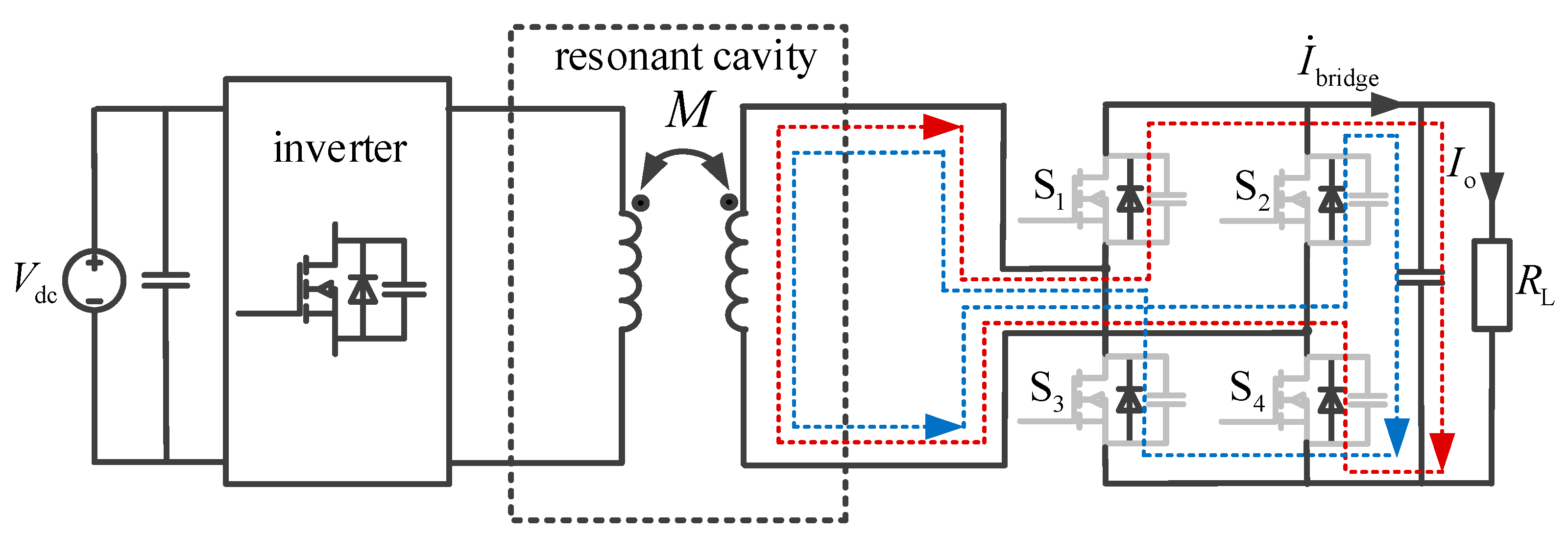
Compared to the SS topology, the DLCC topology incorporates LC links, enhancing parameter design flexibility and potential output power. The proposed method facilitates the transition from CC to CV output while stabilizing the output voltage. By substituting four diodes of the rectifier bridge with MOSFETs, the circuit adopts a symmetrical topology, enabling bidirectional energy flow with proper control.
(2)
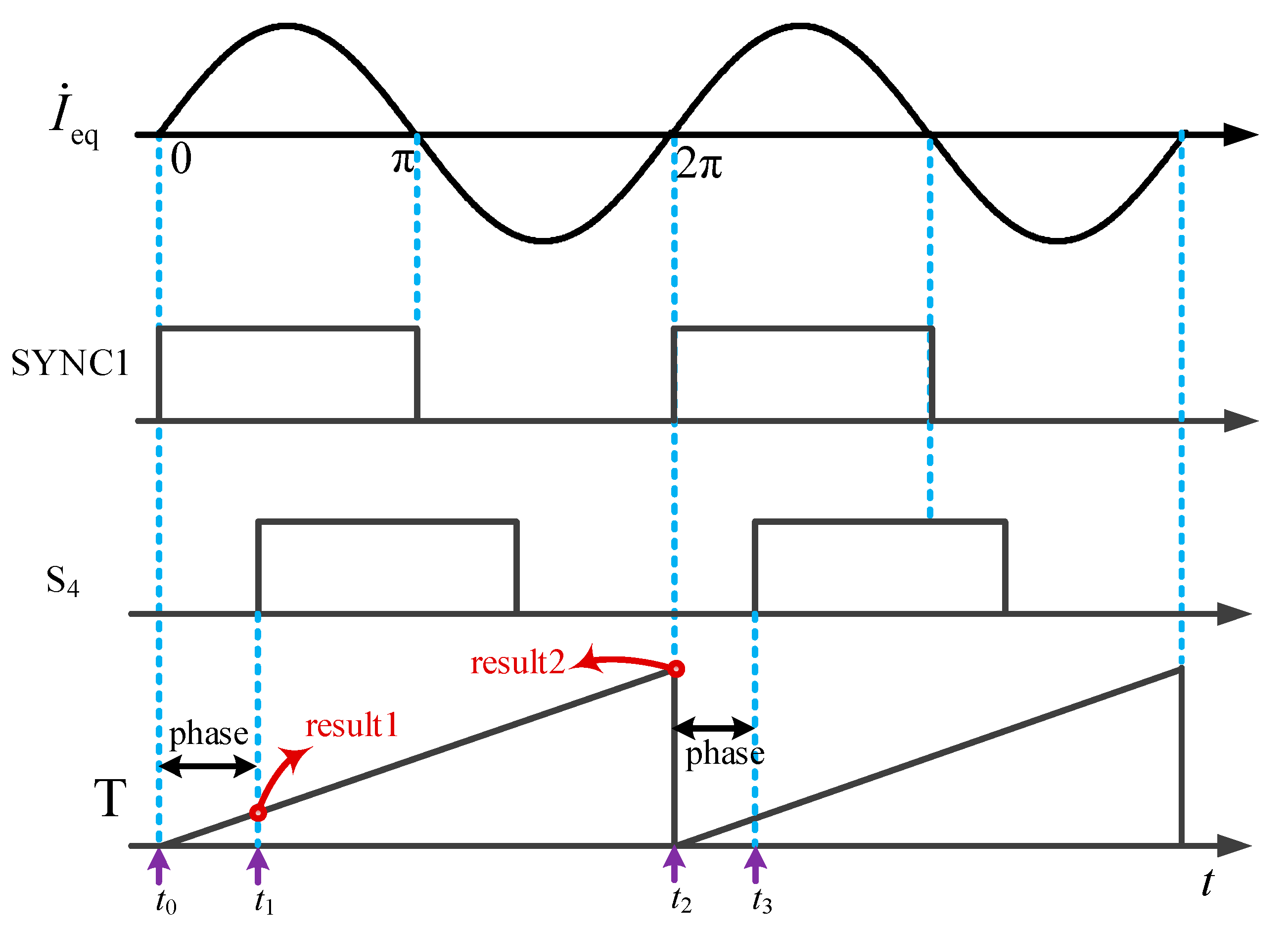
In the method presented herein, switch conduction time is regulated to effectuate the transition from CC to CV output. Additionally, a synchronous signal sampling circuit is introduced to achieve Zero-Voltage Switching (ZVS) conditions in the rectifier bridge, thereby controlling switch conduction sequence. Building upon the conduction time sequence, an output voltage regulation model is derived. A Proportional-Integral-Derivative (PID) control algorithm is employed for CV regulation.
(3)
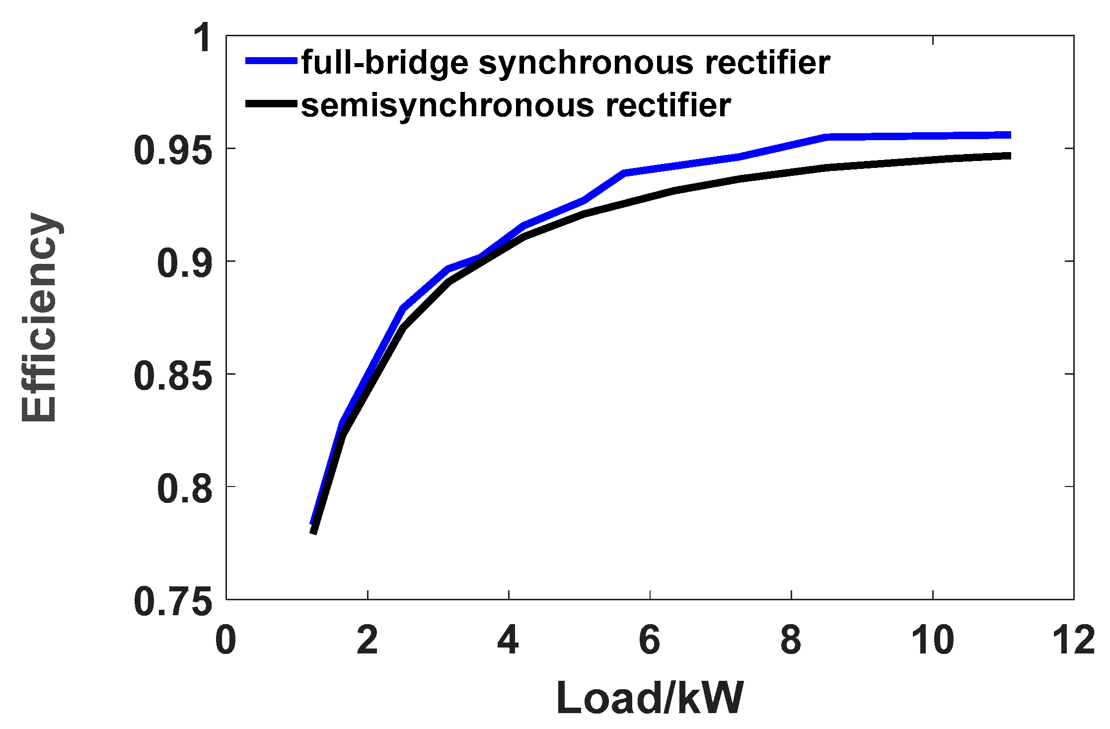
A simulation model and an 11 kW prototype were constructed to validate the proposed design methodology. Results demonstrate that the proposed control method successfully transitions from CC to CV output while maintaining output voltage stability within certain deviations. Moreover, the efficiency of the proposed method surpasses that of the semi-synchronous rectifier.
The organization of this paper is as follows: Section 2 presents a theoretical analysis of circuit structure and input-output characteristics. Section 3 introduces the CVCC control method based on a full-bridge rectifier, including analysis of the ZVS state of diodes, operational mode analysis, and principles of output voltage regulation. Section 4 outlines the design of the controllable synchronous rectifier. Section 5 covers simulation and experimentation. Section 6 comprises a discussion, comparing the proposed method with previous works. Finally, Section 7 concludes the paper.

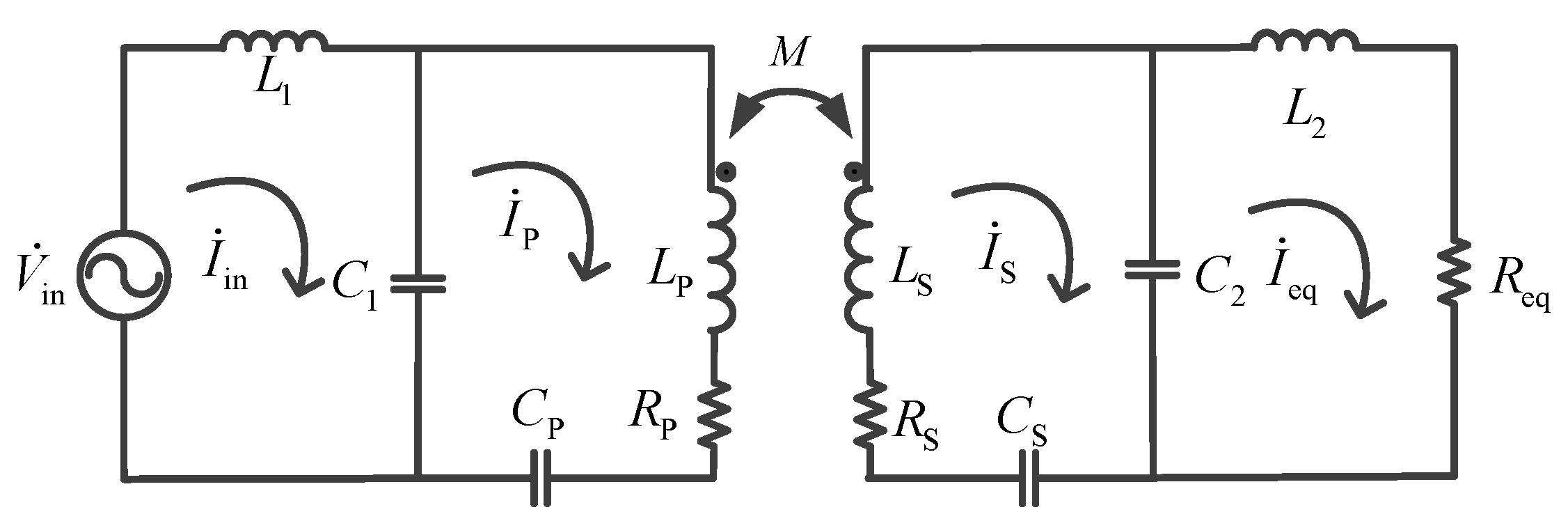
2. Circuit Topological Structure and Theoretical Analysis

2.1. Circuit Topological Structure Analysis

A DLCC compensation structure for both transmitting and receiving compensations is employed to implement the proposed CVCC method as shown in Figure 2. The circuit included a DC power supply, an inverter, an inductance capacitance resonance network, a synchronous signal sampling circuit, a synchronous signal processing circuit, a rectifier driver, a digital signal processing (DSP) or microcontroller unit (MCU), a synchronous rectifier, an output filter circuit, and a load. The DC power supply is linked to the input side of the inverter, with the output side of the inverter connected to the input side of the inductance capacitance resonance network. The output side of the network is then linked to the input side of the synchronous rectifier. High-frequency current signals from the inductance capacitance resonance network are obtained using the synchronous signal sampling circuit. These signals are processed by the synchronous signal processing circuit, converting them into high-frequency voltage signals, which are subsequently filtered, amplified, and transmitted to the DSP/MCU. The DSP/MCU generates pulse-width modulation (PWM) signals sent to the rectifier driver, connected to the synchronous rectifier, which in turn activates the rectification switches. The output of the synchronous rectifier is connected to the input of the filter output circuit, with its output connected to the load.
As shown in Figure 2, the input side was the DC power supply Vdc. Four power MOSFETs, namely, switches Q1 through Q4, together with the body diodes and parasitic capacitors, constituted the full bridge inverter. Q1 and Q3 were complementary in conduction, and they were defined as the leading bridge arms of Q4; Q2, and Q4 were complementary in conduction, and they were defined as hysteresis; Vin and Iin were the output voltage and the output current of the full-bridge inverter circuit, respectively. The parameters in the DLCC type of compensation networks, for example, L1, C1, L2, C2, CP, and CS, along with the coil inductance LP and LS, constituted a resonant cavity. The four power MOSFETs S1 to S4 constituted a controllable full-bridge rectification circuit. A current signal acquisition device was added to the front end of the rectifier. The device processed signals and drove the rectifier. The rectifier circuit converted the secondary high-frequency AC current to the DC current for the load; RL was the load resistance; Vo and Io were the load voltage and current, respectively; Req = 8RL/π2 was the equivalent resistance of the load resistance and the full-bridge rectifier; and Veq and Ieq were the voltage and the current of the equivalent resistance, respectively.

2.2. Analysis of Input and Output Characteristics

According to the energy transmission characteristics of the coupling coils, the system structure shown in Figure 2 was simplified to obtain an equivalent circuit diagram of the DLCC IPT system, as shown in Figure 3. Vin was the square wave voltage output by the inverter module; and Iin was the output current of the inverter. The capacitance had a filtering effect on the high-order harmonics of the voltage signal on the primary side. Therefore, the input current filtered by LC, IP, could be regarded as a quasi-sine wave. After the current entered into the transmitting coil LP, it was coupled with the secondary coil through electromagnetic induction, thus generating an induced electromotive potential jωMIP on the secondary side. The current in the secondary coil was IS; RP and RS were the equivalent internal resistances of the coils on the primary and secondary sides, respectively; M was the mutual inductance between the transmitting coil and the receiving coil; and Iin, IP, IS, and Ieq were the corresponding mesh currents, respectively. The component impedances of the circuit were ZL1 = jωL1, ZC1 = 1/jωC1, ZLP = jωLP, ZCP = 1/jωCP, ZLS = jωLS, ZL2 = jωL2, and ZC2 = 1/jωC2. According to Kirchhoff voltage law and Figure 3, the following relationship was obtained:
Z 11 Z 12 Z 13 Z 14 Z 21 Z 22 Z 23 Z 24 Z 31 Z 32 Z 33 Z 34 Z 41 Z 42 Z 43 Z 44 I i n I P I S I eq = V in 0 0 0 ,
where each non-zero element in the above matrix satisfies the following equations:
Z 11 = Z L 1 + Z C 1 Z 12 = Z C 1 = Z 21 Z 23 = Z M = Z 32 Z 34 = Z C 2 = Z 43 Z 44 = Z L 2 + Z C 2 + R e q Z 22 = Z C P + Z L P + Z C 1 + R P Z 33 = Z C S + Z L S + Z C 2 + R S .
To simplify the calculation, Equation (1) is denoted as ZI = V, where I and V represent current and voltage vectors, respectively. Z represents the impedance matrix. According to circuit theory, the impedance matrix and the admittance matrix are inverses of each other. Therefore, the current vector is expressed as Equation (3).
I = Z 1 V ,
where I = [Iin IP IS Ieq]T. Equation (3) can be used to calculate the equivalent input impedance of the system, transconductance of the system, and the system efficiency, as follows:
Z in = V in I in ,
G V V = R e q I eq V in ,
η = I eq 2 R e q r e a l ( V in I in ) .
Because the derivations of the input and output characteristics of the DLCC compensation structure were provided in the existing literature, they are not repeated here, and the conclusions are used [30]. Under the conditions of Equation (7), the system output is the constant current, and the input is the ZPA.
j ω 0 L 1 + 1 j ω 0 C 1 = 0 j ω 0 L 2 + 1 j ω 0 C 2 = 0 j ω 0 L S + 1 j ω 0 C S + 1 j ω 0 C 2 = 0 j ω 0 L P + 1 j ω 0 C 1 + 1 j ω 0 C P = 0 ,
where ω0 is the system resonant frequency. If the coil resistance is ignored, the output current and voltage of the compensation network are expressed, respectively, as follows:
I eq = j ω 0 3 C 1 C 2 M V in V eq = j ω 0 3 C 1 C 2 R e q M V in .
For the inverter to achieve the ZVS operation, it is necessary for the circuit to maintain weak sensibility. The input impedance can be kept in weak sensibility by fine-tuning CP.

3. The CVCC Control Method Based on Full-Bridge Synchronous Rectification

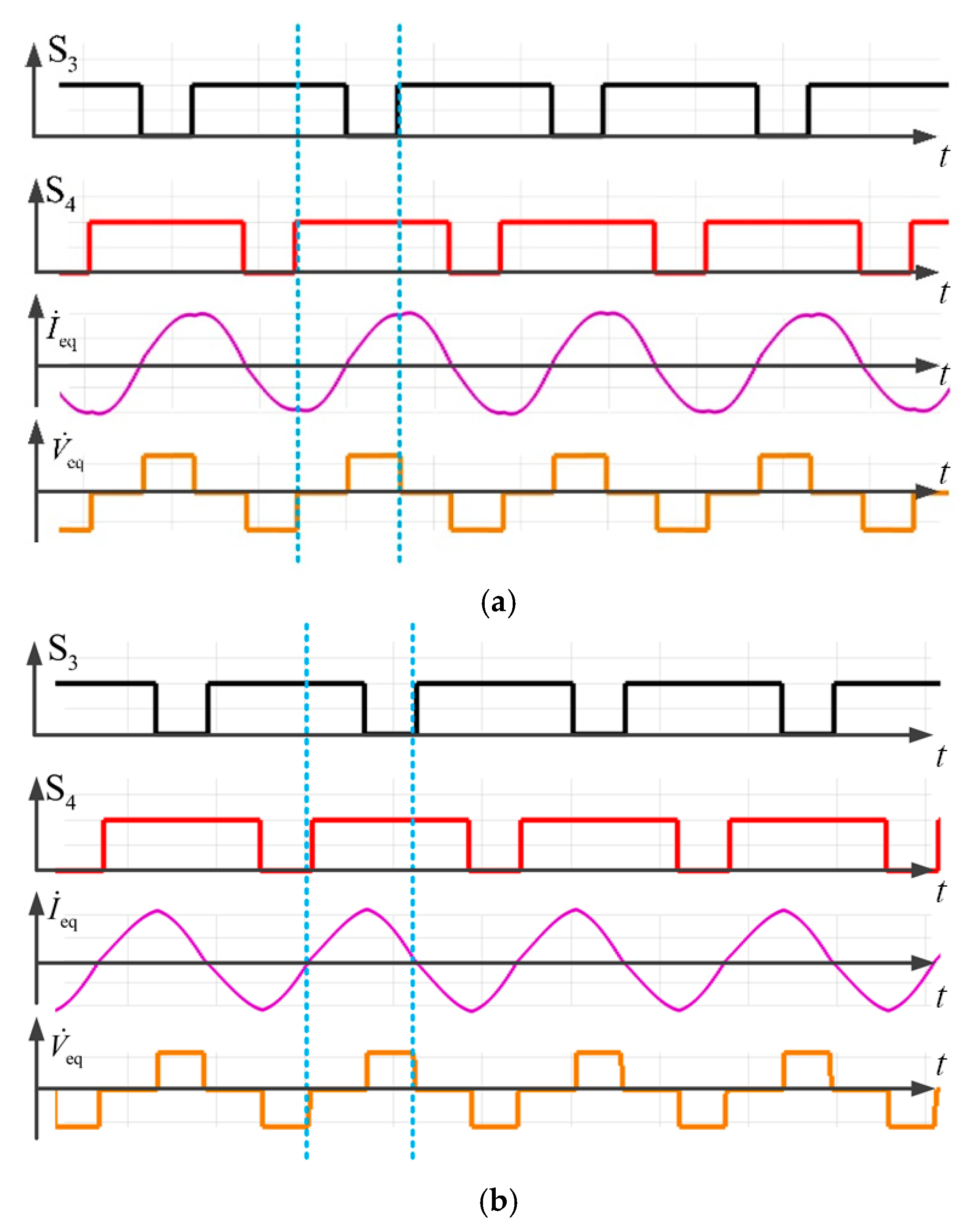
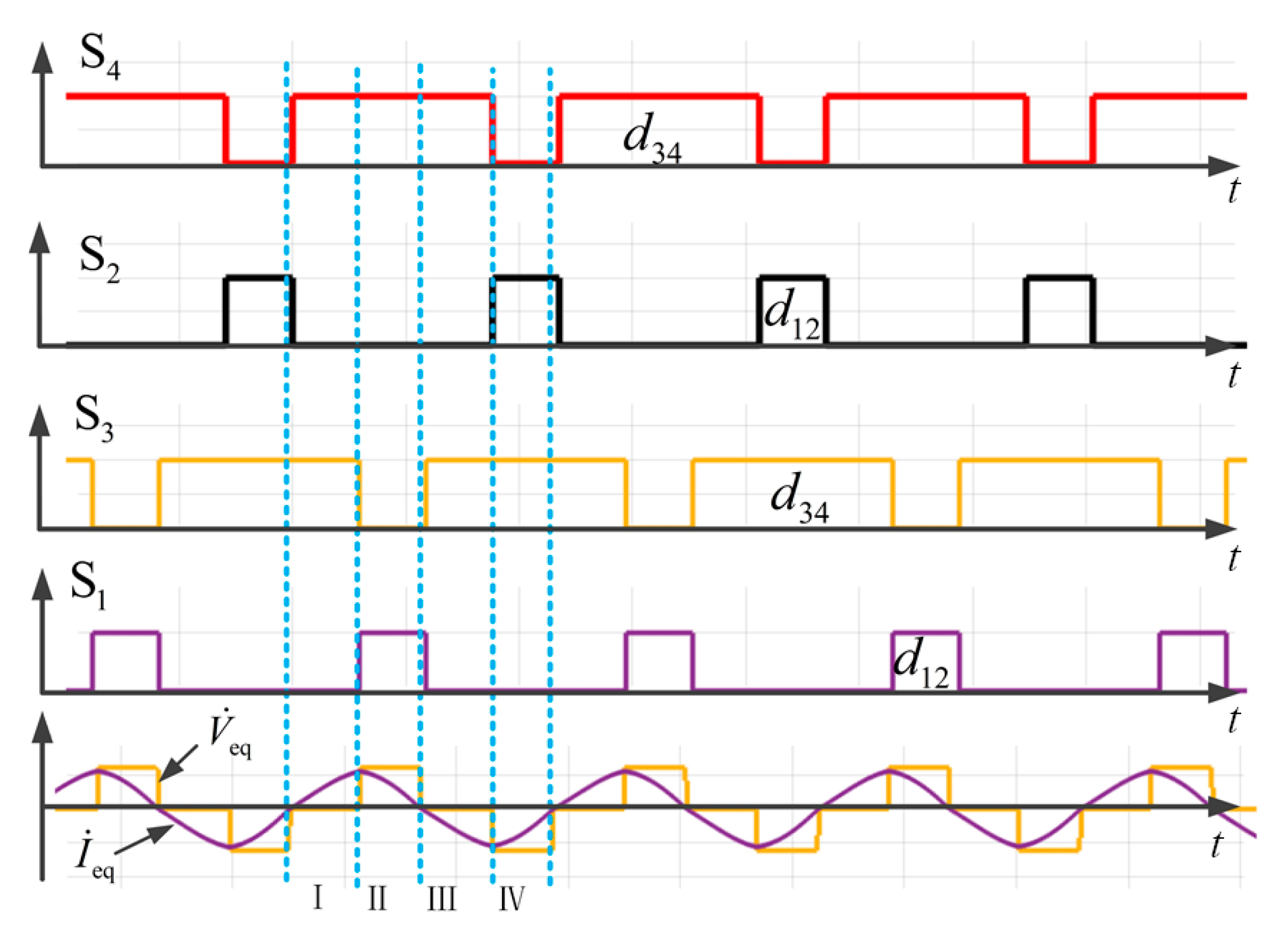
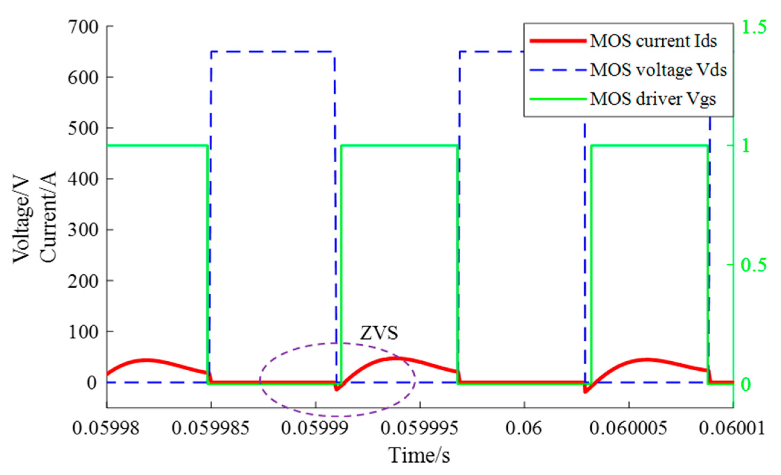
3.1. The Condition with ZVS

From the output characteristics of the DLCC circuit that was under the resonant conditions of Equation (7), the circuit had a CC output, and the current was similar to a sine wave. After the control algorithms were implemented, the full bridge could be controlled on its output, and the CC output could be converted into a CV DC output as a power supply for the load. During the rectification process of the rear-end switches of the full bridge, it was necessary to ensure that the switches worked under the ZVS condition with zero voltage to improve the system efficiency. To realize the ZVS condition of the switches, the diode in reverse parallel with the switch had to be turned on, and the switch had to be turned on before the diode was turned off.
As shown in Figure 4, if the four switches were turned off, during the positive half cycle of the sinusoidal current (the red dotted line), the current flowed through the diodes S1 and S4, and the voltages at the ends of S1 and S4 were approximately zero. When S1 and S4 were turned on during this cycle, the ZVS condition could be achieved for S1 and S4. In contrast, during the negative half cycle of the sinusoidal current (the blue dotted line), the current flowed through the diodes S2 and S3. When S2 and S3 were turned on during this cycle, the ZVS condition could be achieved for S2 and S3.
The Simulink simulation results in Figure 5 show the driving waveforms of the switches and the output voltage and current waveforms of the compensation network when the switches were under a hard switch-on condition and the ZVS condition. To prevent the straight-through phenomenon of the switches on the same bridge arm, the driving signals of the switches on the same bridge arm were complementary. Therefore, the driving waveforms of S1 and S2 are omitted in Figure 4. More interpretation is provided in the operating mode analysis in the next section.
As shown in Figure 5a, the rising edge of the driving signal of S4 was in the negative half cycle of the output current of the compensation network. At that moment, the voltages at both ends of S4 were equal to the output voltage of the compensation network and decreased rapidly to zero. Therefore, the energy stored by the junction capacitor in S4 was consumed on the switch S4, indicating a hard switch-on condition of S4. Similarly, the rising edge of the driving signal of S3 was in the positive half cycle of the output current of the compensation network. At this moment, the voltages at both ends of S3 were equal to the output voltage of the compensation network, and they decreased rapidly to zero, indicating a hard switch-on condition of S3. It was observed that when the switch was turned on under the hard condition, the input current waveform of the compensation network exhibited a sunken shape.
As shown in Figure 5b, the rising edge of the driving signal of S4 was in the positive half cycle of the output current of the compensating network after zero-crossing. At this moment, the voltages at both ends of S4 were zero and kept at zero, leading to the ZVS condition of S4. Similarly, the rising edge of the driving signal of S3 was in the negative half cycle of the output current Ieq of the compensating network after zero-crossing. At this moment, the voltages at both ends of S3 were zero and stayed at zero, leading to the ZVS condition of S3. We also observed that when the switch was under the condition of zero voltage, the input current waveform of the compensation network exhibited a smooth shape when the switch was turned on.

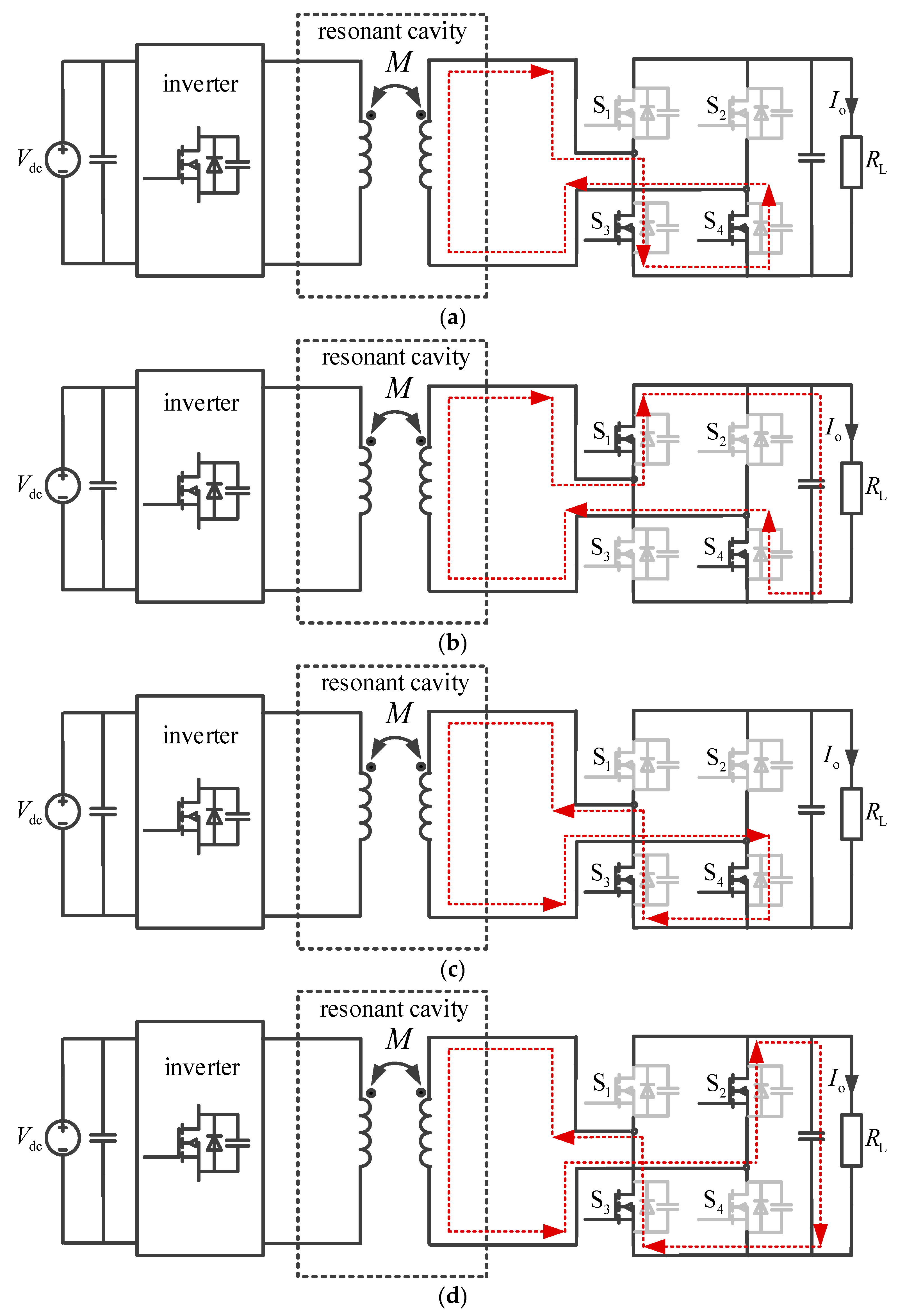
3.2. Operating Mode Analysis

The previous section analyzed the ZVS condition of the switches in the rectification circuit. This section analyzes the operating modes of the circuit in detail. Figure 6 shows the driving waveforms of the switches under the ZVS condition and the output voltage and current waveforms of the compensation network. In the symmetric control mode, the duty cycles of the switches S3 and S4 were the same, represented by d34 (0.5 ≤ d34 ≤ 1). When the duty cycles of the switches S1 and S2 were the same, such a condition was represented by d12. The driving waveform of S1 was complementary to that of S3 on the same bridge arm. The driving waveform of S2 was complementary to that of S4 on the same bridge arm. Moreover, d12 = 1 − d34.
Figure 7 shows the current paths of the four operating modes of the rectification circuit. Each mode is described as follows:
Mode I: As shown in Figure 7a, in this mode, the output current of the compensation network was at a reverse point, and the current changed from negative to positive. Under the action of the synchronous signal, S2 was shut off, and S4 was turned on. Because S4 was turned on in the positive half cycle of the output current of the compensation network, S4 was switched on under zero voltage. Because S1 remained off and S3 remained on, the output current of the compensation network flowed through S3 and S4 and returned to the compensation network. The load resistor was short-circuited, resulting in zero-output voltage of the compensation network, and the voltage remained at zero.
Mode II: As shown in Figure 7b, in this mode, the output current of the compensation network was in the positive half cycle; S3 was off, and S1 was on. Because S1 was turned on in the positive half cycle, S1 was switched on under zero voltage. Because S2 remained off and S4 remained on, the output current of the compensation network flowed through S1, the load resistance, and S4. The output voltage of the compensation network was the voltage at both ends of the load.
Mode III: As shown in Figure 7c, in this mode, the output current of the compensation network was at a reverse point, and the current changed from positive to negative. Under the action of the synchronous signal, S1 was shut off, and S3 was turned on. Because S3 was turned on in the negative half cycle of the output current of the compensation network, S3 was switched on under zero voltage. Because S2 remained off and S4 remained on, the output current of the compensation network flowed through S3 and S4, and then returned to the compensation network. The load resistor was short-circuited, resulting in zero-output voltage of the compensation network, and the voltage was kept at zero.
Mode IV: As shown in Figure 7d, in this mode, the output current of the compensation network was in a negative half cycle; S4 was off, and S2 was on. Because S2 was turned on in the negative half cycle, S2 was switched on under zero voltage. Because S1 remained off and S3 remained on, the output current of the compensation network flowed through S2, the load resistance, and S3. The output voltage of the compensation network was the voltage at both ends of the load.

3.3. Output Voltage Regulation Model

According to the ZVS condition, when the switches S1 and S4 were turned on in the positive half cycle of the output current of the compensating network, or when the switches S2 and S3 were turned on in the negative half cycle, the switches could achieve the ZVS condition. In addition to the requirement of operating under the ZVS condition, the system also had to achieve the maximum power output, which occurred in one of the following two scenarios in which all of the output current flowed through the load: (1) when S1 and S4 were turned on in the entire positive half cycle and turned off in the entire negative half cycle; and (2) when S2 and S3 were turned on in the entire negative half cycle and turned off in the entire positive half cycle. The fully controlled rectification bridge was connected with a voltage capacitor to output the current Ibridge. The current was then filtered into the DC current Io with smaller ripples to power the load. The output current waveforms are shown in Figure 8.
The peak value of the output current of the rectification bridge was assumed to be Ipk. Then, Ipk = 2 |Ieq|. The average value of the output current was Io. Figure 8a shows that the maximum output current and the maximum output voltage of the system can be calculated at the maximum power output as follows:
I omax = I pk 0 π sin α d α π = 2 I pk π ,
V omax = I omax R L = 2 I pk R L π ,
where α is the angle of the integration interval.
According to the preceding analysis of operating modes, in a symmetric control setting, the duty cycles of switches S3 and S4 were identical, denoted as d34, while those of switches S1 and S2 shared the same value, represented by d12. Additionally, the driving waveform of S1 was complementary to that of S3 within the same bridge arm, and similarly, the driving waveform of S2 complemented that of S4 on the same bridge arm. Under these conditions, the conduction angle of the rectification circuit was 2πd12. Figure 8b shows the output current waveform of the rectification circuit corresponding to this conduction angle. Therefore, the output current and voltage of the system can be calculated as follows:
I o = I pk π 2 π d 12 π sin α d α π = I pk π 1 cos ( 2 π d 12 ) ,
V o = I o R L = I pk R L π 1 cos ( 2 π d 12 ) ,
where the range of d12 is [0, 0.5], and the range of conduction angle is [0, π]. As the conduction angle increases, the output voltage increases. The regulation range of the output voltage is between 0 and Vomax.
From Equation (12), the relationship between the system output voltage and the duty cycle d12 is evident. Let us define the system’s equilibrium operating point A (d12_0, VO_0) and perform a Taylor series expansion at point A, neglecting higher-order terms, we obtain the following:
V o V o _ 0 = 2 I pk R L sin ( 2 π d 12 ) ( d 12 d 12 _ 0 ) ,
where ΔVO = VOVO_0, Δd12 = d12d12_0, K = 2IpkRLsin(2d12_0). Here, the linear equation can be simplified to ΔVO = KΔd12, where K represents a proportionality coefficient. It signifies the tangent slope of function VO at operating point A, reflecting the rate of change of the output voltage at that point. Since d12 ranges from 0 to 0.5, K is a positive real number. The output voltage variation is fastest when the duty cycle is 0.25, while it is slowest at duty cycles of 0 and 0.5 in the rectifier circuit.

4. Compensation Network Design Development of the Synchronous Rectifier

4.1. Controllable Rectifier Design

The power block diagram of the controllable rectifier module on the secondary side is shown in Figure 9. The design of the controllable rectifier was basically the same as that of the high-frequency inverter on the primary side. The major difference was adding a zero-crossing current detection circuit to realize accurate conduction of the rectifier tube. Current sampling was achieved by using 1000:1 Hall coils. The voltage was applied to the series resistances at the output end of the Hall coils. Square wave signals SYNC1 and SYNC2 were obtained after the first-stage and second-stage amplifiers. The zero-crossing current signals were used to judge the function of the MOSFET switch in the synchronous rectifier.

4.2. Implementation of Phase-Locked Loop

Figure 10 shows the schematic diagram of the principle of the phase-locked loop (PLL) with synchronous rectification. The capture (CAP) function port in DSP initialization was set up as the time base of the capture port. The trigger of the rising edge of the capture port was also defined. At time t0, the rising edge of the synchronous sampling signal SYNC1 appeared, and the internal counter T was cleared to start counting. At time t1, the rising edge’s jump of the S4 synchronous rectifier tube was detected, and the count value of T, Nresult1, was sent into the register “result1” corresponding to the capture port. At time t2, the rising edge’s jump of SYNC1 in the next cycle was captured, and the count value of T, Nresult2 was sent into the register “result2.” Then, the internal counter T was cleared to zero to start counting for the next cycle.
Therefore, the phase difference between the synchronous sampling signal SYNC1 and the synchronous rectifier tube S4 can be expressed as follows:
α P L L = 2 π N r e s u l t 1 N r e s u l t 2
If the calculated phase difference was in the range of 1° to 180°, the phase of S4 lagged behind SYNC1. If the calculated phase difference was in the range of 180° to 359°, the phase of S4 led SYNC1. If the calculated absolute value was less than 1°, phase locking was successful.

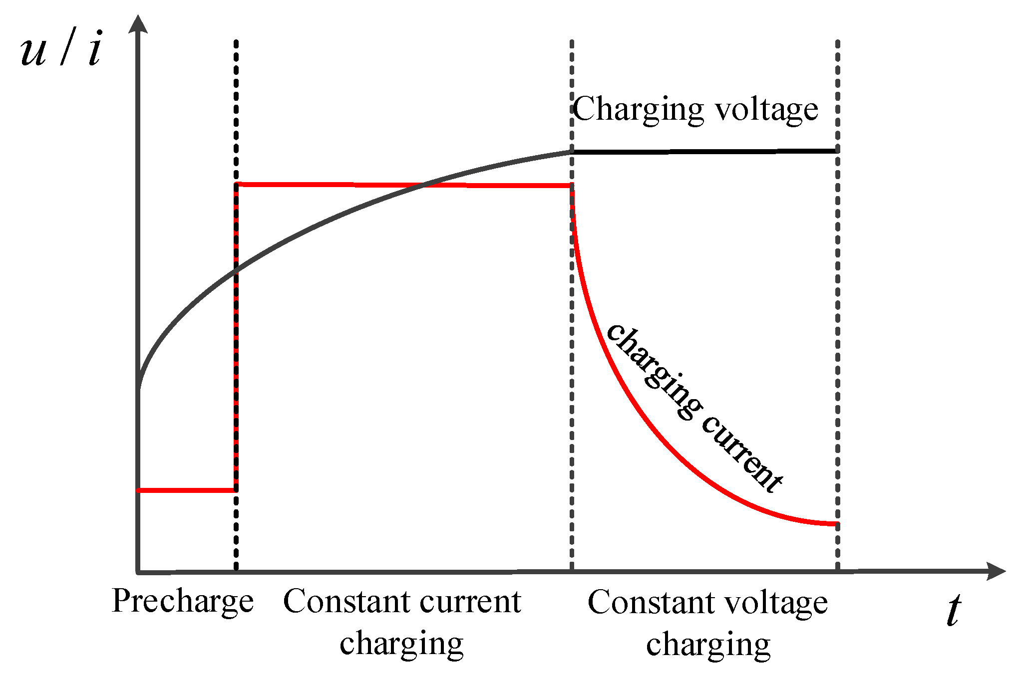
5. Simulation and Experimental Validation

To validate the proposed design method, we used MATLAB/Simulink 2018a simulation models and a set of 11 kW principle prototypes to produce both computational and experimental verification data. According to the system parameters derived from the theory in Section 2, the components of the compensation network can be calculated from Equations (7) and (8). The parameters used in the validation are given in Table 1.

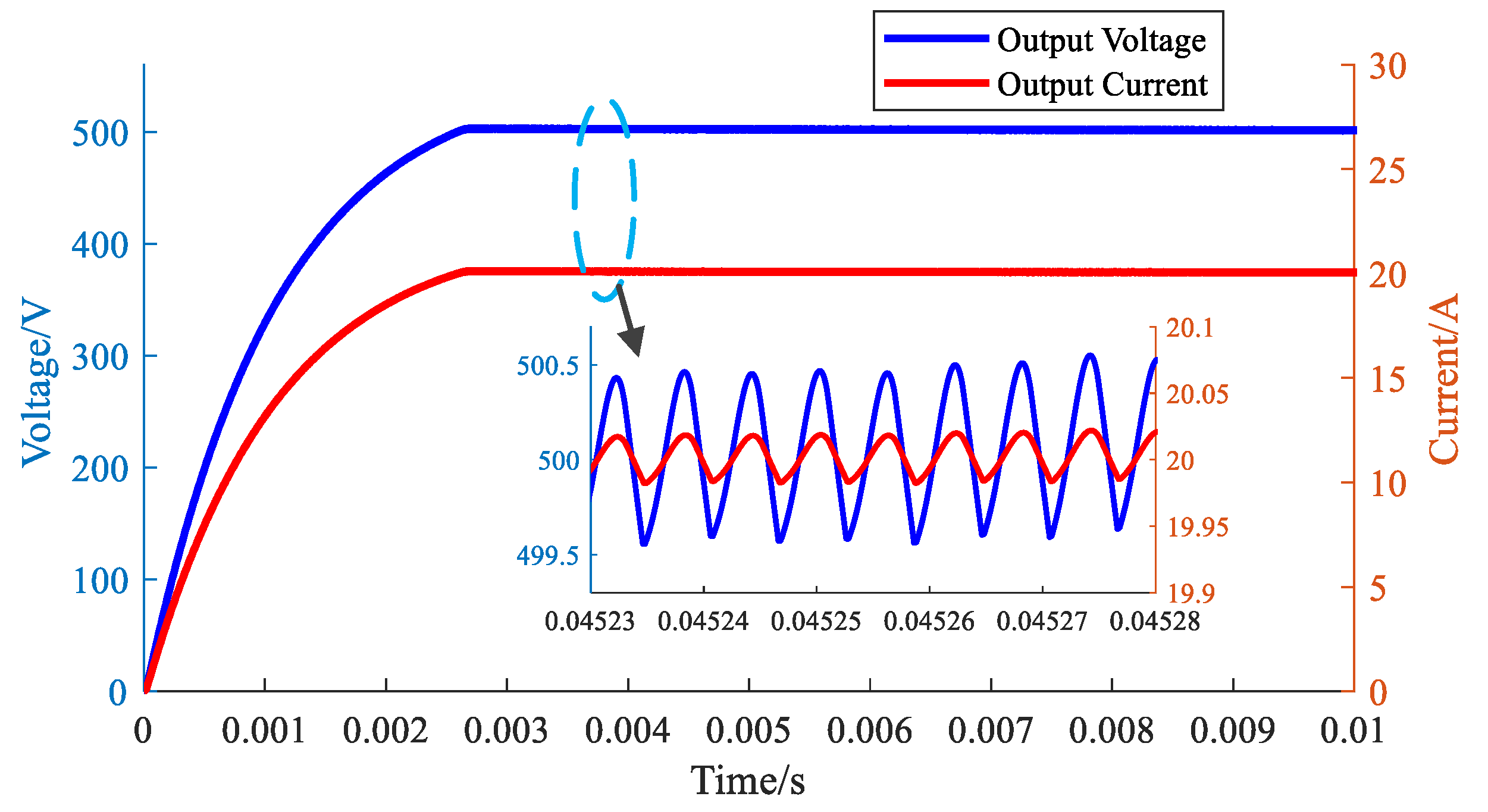
5.1. Simulation Analysis of the Soft Startup Process

During startup, the duty cycle of the MOSFET on the secondary side rectifier was 1. The duty cycle gradually decreased to achieve the CV output.
Throughout this procedure, the output voltage steadily rose to facilitate a soft startup. As depicted in Figure 11, the waveform of the output voltage and current during startup under the rated load illustrates this progression. Notably, the voltage ascended gradually to the predetermined level with minimal overshooting, while the current exhibited a steady increase, also without overshooting, ensuring a seamless startup. Following startup, the voltage exhibited fluctuations within the range of 499.5 to 500.5 V, with a voltage ripple of 1 V, while the current fluctuated between 19.95 and 20.05 A, with a current ripple of 0.1 A. These findings underscore the efficacy of the proposed design methodology. Further discussions will delve into the simulation and experimental results pertaining to the CV output characteristics at varying loads.
Figure 12 shows the ZVS waveform of the MOSFETs. When the Vds of the MOSFET switch decreased to 0, Vgs increased to a high level and achieved the ZVS condition with reduced switch-on losses of MOSFET.

5.2. Simulation Analysis of Dynamic Characteristics

After the system was started without any load, the load was successively added to 25%, 50%, 75%, and 100% at 0.05 s, 0.1 s, 0.15 s, and 0.2 s, respectively. The voltage and current waveforms during the loading process are shown in Figure 13. During the loading process, the output voltage decreased to 495 V, with approximately 1% reduction, and the current did not overshoot. The CV output was achieved at approximately 20 ms during each loading.
During the process of no-load startup, the voltage on the load had very little overshooting. The peak voltage was 510 V, with only 2% overshooting, and the current did not have any overshooting.

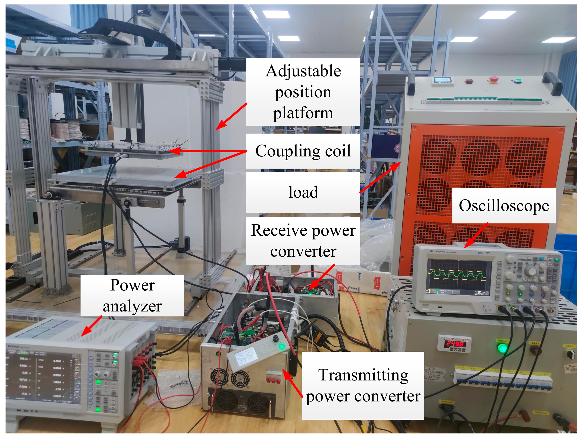
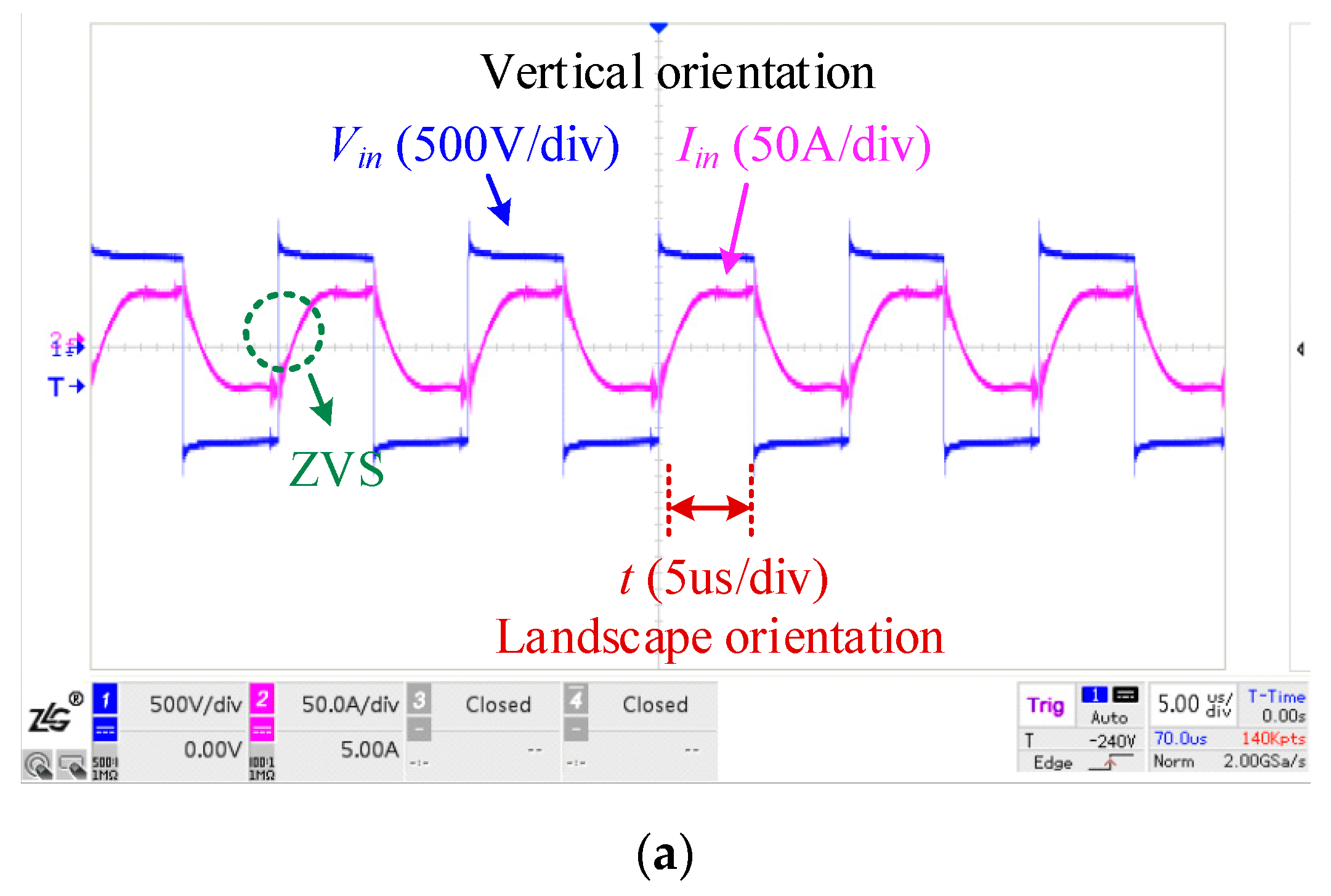
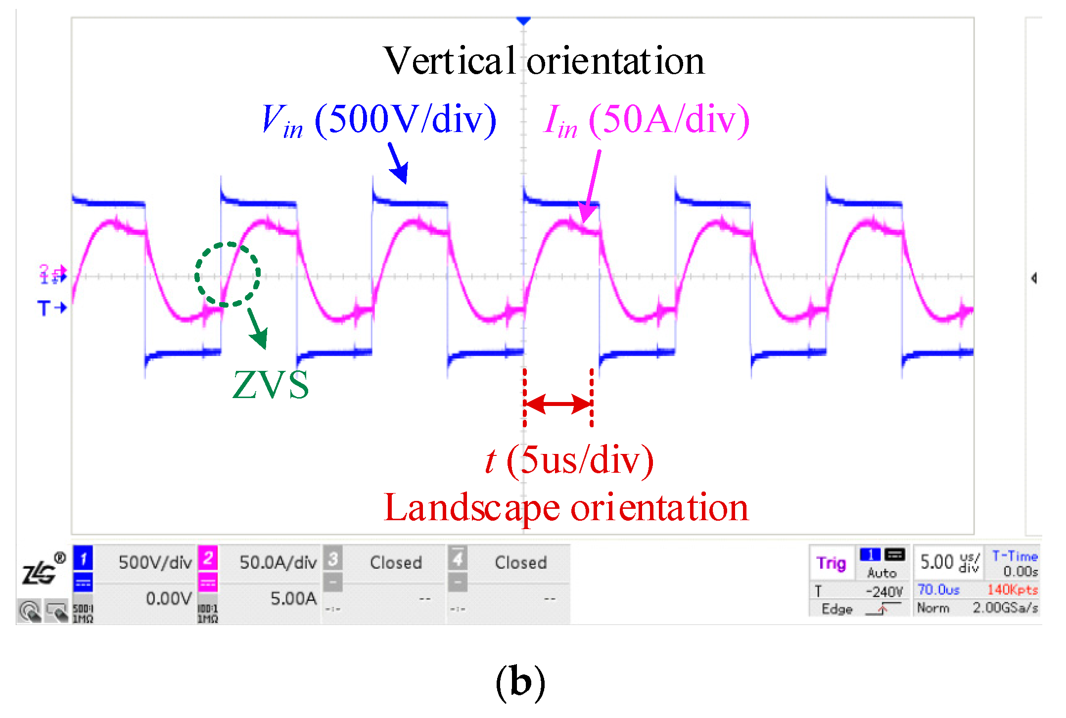
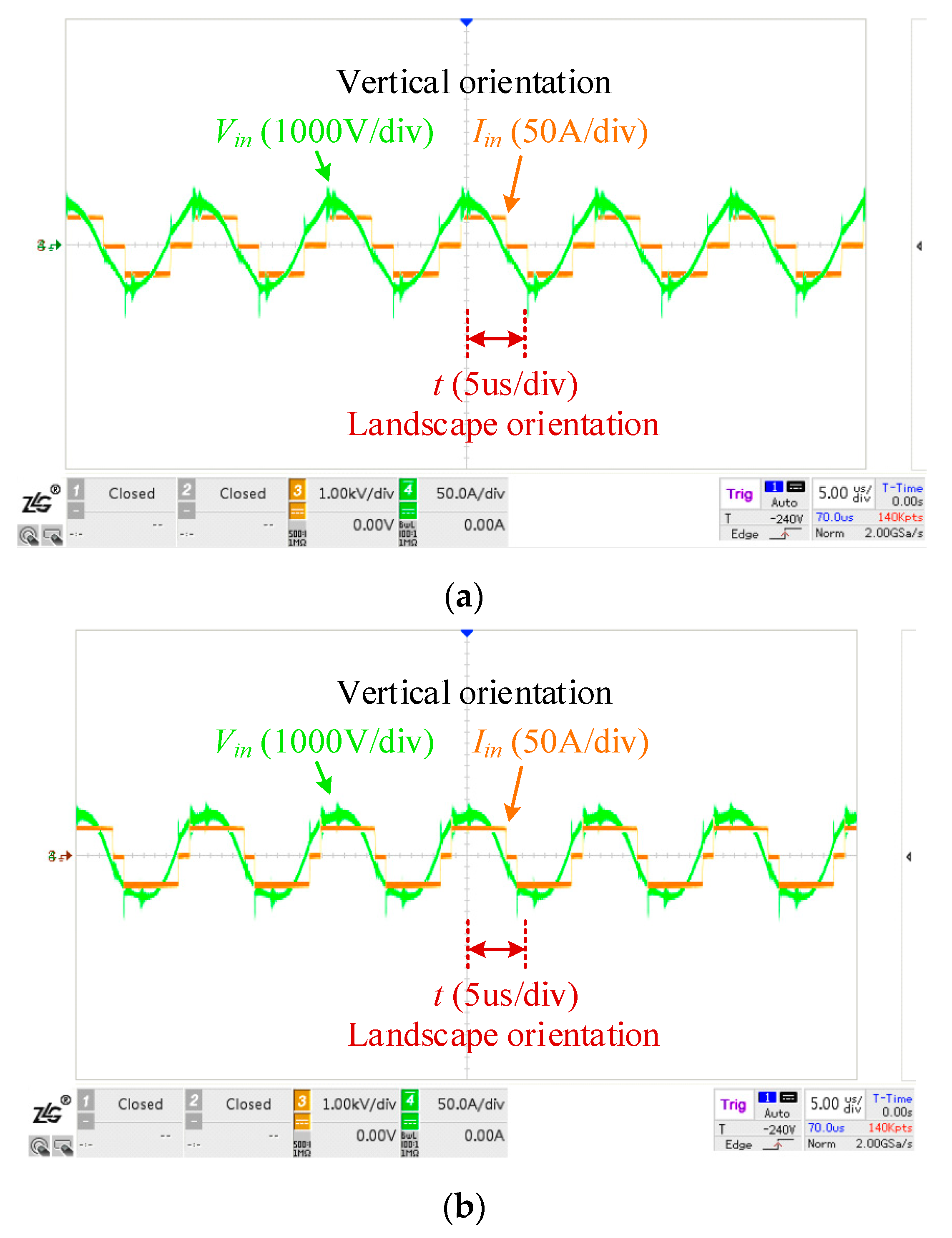
5.3. Analysis of Experimental Results

To validate the theoretical analysis, a physical experiment platform of the IPT system was built. The platform used B1M040120HC silicon carbide power MOSFET to constitute the full-bridge inverter circuit and the rectification circuit. The driver integrated circuit used the enhanced isolation ISO5852S driver chip. The control module used the TMS320F280049 chip. To increase the resonance quality factor of the transmission coils to avoid magnetic saturation, the coils were wound with the Litz wire. Ferrite was tiled at the bottom of the coils, and an aluminum plate was used as a shielding layer. The output voltage frequency of the inverter was 85 kHz. The distance between the transmitting and receiving coils was 100 mm. The measured coupling coefficient was 0.19. The experimental platform is shown in Figure 14.
This experiment was conducted according to the parameters listed in Table 1 to obtain the input and output waveforms of the system at different loads. The test data was recorded, and the results are shown in Figure 15, Figure 16, Figure 17 and Figure 18. Figure 15 shows the waveforms of the output voltage and current of the inverter at different loads. Figure 16 shows the waveforms of the output voltage and current of the compensation network at different loads. Both Figure 15 and Figure 16 feature screenshots from the oscilloscope. The model of the oscilloscope is ZDS3024, manufactured by Zhiyuan Electronics in Guangzhou, China. Figure 17 shows the test data of the voltage gains of the system at different loads. Figure 18 shows the test data of the system efficiencies of the full-bridge synchronous rectification and semi synchronous rectification at different loads.
Figure 15 shows that at different loads, the output voltage of the inverter always led the output current, and the input impedance of the system was weakly inductive. These conditions ensured that the inverter was able to function properly under the ZVS condition.
Figure 16 shows that at different loads, the output current of the compensation network was constant. Therefore, the DLCC compensation structure had good CC characteristics. The duty cycle of the output voltage of the compensation network increased with the increase in the load. To maintain the CV output, when the output voltage decreased, the switch-on time of the switch under the rectifier had to decrease to increase the switch-on time on the load side, so that the CV output could be maintained. When the output voltage increased, the switch-on time of the switch under the rectifier had to increase to short-circuit the load side to reduce the switch-on time on the load side, so that the CV output could be maintained.
Figure 17 shows the experimental data of the voltage gains at different loads. We observed that the output voltage was always stable. When the coupling coil was offset by 100 mm, the system was able to maintain the same CV output characteristics. These results further verified that the proposed design method was accurate.
Figure 18 shows that the system output efficiencies of the two rectification methods increased with the increase in the load and reached the maximum at the rated load. Moreover, the system output efficiency of the full-bridge synchronous rectifier was higher than that of the semi synchronous rectifier, reaching the maximum efficiency of 95.6% at the rated load. The conduction loss of the MOSFETs was less than that of the diode when the soft switch-on condition was used.

6. Discussion

To effectively evaluate the proposed approach and clearly demonstrate the improvements achieved using the proposed method, this paper contrasts with some typical IPT systems featuring CVCC output characteristics. The comparative results are presented in Table 2. Refs. [10,11] analyzed and designed the CVCC state of IPT systems based on LCC-S and DLCC compensation networks, respectively, and validated them using a 3.3 kW prototype, with maximum efficiencies of 89.2% and 92.9%, respectively. Ref. [12] employed a hybrid topology, utilizing switching between two different characteristic compensation networks to achieve CV and CC switching, validated with a 0.12 kW prototype, achieving a maximum efficiency of 92.2%. Ref. [26] realized CVCC operation by adding a Boost converter on the secondary side, with power and efficiency of 0.5 kW and 92.9%, respectively. It is noteworthy that Refs. [12,26] introduced more complex structures, inevitably leading to a decrease in power density. Ref. [29] utilized a semi-synchronous rectifier, with a more compact structure, achieving power and efficiency of 2.5 kW and 88%, respectively.
Compared to previous studies, this work combines the advantages of DLCC compensation networks and controllable synchronous rectifiers, resulting in significant improvements in output power and efficiency. Moreover, without adding additional cascaded modules, the power density is higher. The established prototype achieved an output power of 11 kW and an efficiency of 95.6%, demonstrating the effectiveness and advancement of the proposed method.
While the proposed method demonstrates promising results, there are some limitations to consider. For example, in harsh environments, wireless communication may encounter difficulties; system performance may be affected by sudden changes in load and coupling; and eddy current losses in underwater transmission significantly increase system impedance, leading to decreased control precision, among other issues. Future work could focus on developing adaptive control strategies to mitigate these effects and further enhance system efficiency and robustness. Additionally, exploring advanced modulation techniques and optimization algorithms could lead to even greater improvements in IPT system performance.

7. Conclusions

This paper presents a dynamic voltage regulation control method for the secondary side circuit in the IPT system, utilizing the DLCC compensation structure to achieve CVCC output. Employing the DLCC compensation structure enables CC output realization. The secondary side circuit employs a full-bridge rectification topological structure to adjust the conduction time of the rectifier bridge switches, facilitating the transition from CC output to CV output. We delve into the conditions and control methods necessary to attain the ZVS condition for the full-bridge controllable rectifier. Additionally, a simulation model and an 11 kW prototype were constructed to validate the proposed design approach. Results demonstrate that the proposed system exhibits favorable CV output characteristics and maintains a constant output amidst certain interference from coupling offset.
In conclusion, this study demonstrates the effectiveness of the proposed dynamic voltage regulation control method for achieving CVCC output in the IPT system. Through simulation analysis and experimental validation, it is evident that the system maintains stable CV output characteristics and exhibits high efficiency, particularly with the utilization of the full-bridge synchronous rectifier. Furthermore, the proposed design method proves to be robust against certain interference conditions, highlighting its practical applicability in real-world scenarios.

Author Contributions

Conceptualization, J.C. and P.S.; methodology, J.C., P.S. and K.J.; validation, J.C., H.J. and Y.W.; investigation, J.C., P.S. and X.W.; writing—original draft preparation, J.C.; writing—review and editing, P.S., K.J., X.W., H.J., Y.W. and E.R.; funding acquisition, P.S. and X.W. All authors have read and agreed to the published version of the manuscript.

Funding

This research was funded by the National Key Research and Development Program of China (Grant No. 2022YFC3102800), the National Natural Science Foundation of China Youth Project (Grant No. 52007195), and the Natural Science Foundation of Hubei Provincial (Grant No. 2018CFA008).

Data Availability Statement

Data are contained within the article.

Conflicts of Interest

The authors declare no conflicts of interest.

References

  1. Mansouri, A.; El Magri, A.; Lajouad, R.; Giri, F. Control design and multimode power management of WECS connected to HVDC transmission line through a Vienna rectifier. Int. J. Electr. Power-Energy Syst. 2024, 155, 109563. [Google Scholar] [CrossRef]
  2. Mansouri, A.; El Magri, A.; Lajouad, R.; Myasse, I.E.; Younes, E.K.; Giri, F. Wind energy based conversion topologies and maximum power point tracking: A comprehensive review and analysis. e-Prime-Adv. Electri. Eng. Electron. Energy 2023, 6, 100351. [Google Scholar] [CrossRef]
  3. Xie, R.; Liu, R.; Chen, X.; Mao, X.; Li, X.; Zhang, Y. An Interoperable Wireless Power Transmitter for Unipolar and Bipolar Receiving Coils Based on Three-Switch Dual-Output Inverter. IEEE Trans. Power Electron. 2024, 39, 1985–1989. [Google Scholar] [CrossRef]
  4. Zhou, W.; Tang, D.; Chen, Z.; Mai, R.; He, Z. Nonisolation Model and Load Virtual-Grounding Design Method for Capacitive Power Transfer System with Asymmetric Four-Plate Coupling Interface. IEEE J. Emerg. Sel. Top. Power Electron. 2024, 12, 208–218. [Google Scholar] [CrossRef]
  5. Liao, Z.-J.; Wu, F.; Jiang, C.-H.; Chen, Z.-R.; Xia, C.-Y. Analysis and Design of Ideal Transformer-Like Magnetic Coupling Wireless Power Transfer Systems. IEEE Trans. Power Electron. 2022, 37, 15728–15739. [Google Scholar] [CrossRef]
  6. Li, S.; Duan, H.; Xia, J.; Xiong, L. Analysis and Case Study of National Economic Evaluation of Expressway Dynamic Wireless Charging. Energies 2022, 15, 6924. [Google Scholar] [CrossRef]
  7. Chen, Y.; Zhang, Z.; Yang, B.; Zhang, B.; Fu, L.; He, Z.; Mai, R. A Clamp Circuit-Based Inductive Power Transfer System with Reconfigurable Rectifier Tolerating Extensive Coupling Variations. IEEE Trans. Power Electron. 2024, 39, 1942–1946. [Google Scholar] [CrossRef]
  8. Zhou, Y.; Qiu, M.; Wang, Q.; Ma, Z.; Sun, H.; Zhang, X. Research on Double LCC Compensation Network for Multi-Resonant Point Switching in Underwater Wireless Power Transfer System. Electronics 2023, 12, 2798. [Google Scholar] [CrossRef]
  9. Li, T.; Li, S.; Liu, Z.; Fang, Y.; Xiao, Z.; Shafiq, Z.; Lu, S. Enhancing V2G Applications: Analysis and Optimization of a CC/CV Bidirectional IPT System with Wide Range ZVS. IEEE Trans. Transp. Electrif. 2024, in press. [CrossRef]
  10. Lu, J.; Zhu, G.; Lin, D.; Zhang, Y.; Mi, C.C. Unified Load-Independent ZPA Analysis and Design in CC and CV Modes of Higher Order Resonant Circuits for WPT Systems. IEEE Trans. Transp. Electrif. 2019, 5, 977–987. [Google Scholar] [CrossRef]
  11. Lu, J.; Zhu, G.; Lin, D.; Wong, S.; Jiang, J. Load-Independent Voltage and Current Transfer Characteristics of High-Order Resonant Network in IPT System. IEEE J. Emerg. Sel. Top. Power Electron. 2019, 7, 422–436. [Google Scholar] [CrossRef]
  12. Li, G.; Jo, C.-H.; Shin, C.-S.; Jo, S.; Kim, D.-H. A Load-Independent Current/Voltage IPT Charger with Secondary Side-Controlled Hybrid-Compensated Topology for Electric Vehicles. Appl. Sci. 2022, 12, 10899. [Google Scholar] [CrossRef]
  13. Yang, L.; Geng, Z.; Jiang, S.; Wang, C. Analysis and Design of an S/PS−Compensated WPT System with Constant Current and Constant Voltage Charging. Electronics 2022, 11, 1488. [Google Scholar] [CrossRef]
  14. Vu, V.-B.; Tran, D.-H.; Choi, W. Implementation of the Constant Current and Constant Voltage Charge of Inductive Power Transfer Systems with the Double-Sided LCC Compensation Topology for Electric Vehicle Battery Charge Applications. IEEE Trans. Power Electron. 2018, 33, 7398–7410. [Google Scholar] [CrossRef]
  15. Rong, C.; Duan, X.; Chen, M.; Wang, Q.; Yan, L.; Wang, H.; Xia, C.; He, X.; Zeng, Y.; Liao, Z. Critical Review of Recent Development of Wireless Power Transfer Technology for Unmanned Aerial Vehicles. IEEE Access 2023, 11, 132982–133003. [Google Scholar] [CrossRef]
  16. Zhou, W.; Gao, Q.; Mai, R.; He, Z.; Hu, P. Design and Analysis of a CPT System with Extendable Pairs of Electric Field Couplers. IEEE Trans. Power Electron. 2022, 37, 7443–7455. [Google Scholar] [CrossRef]
  17. Xia, J.; Yuan, X.; Lu, S.; Dai, W.; Li, T.; Li, J.; Li, S. A General Parameter Optimization Method for a Capacitive Power Transfer System with an Asymmetrical Structure. Electronics 2022, 11, 922. [Google Scholar] [CrossRef]
  18. Rong, E.; Sun, P.; Qiao, K.; Zhang, X.; Yang, G.; Wu, X. Six-Plate and Hybrid-Dielectric Capacitive Coupler for Underwater Wireless Power Transfer. IEEE Trans. Power Electron. 2024, 39, 2867–2881. [Google Scholar] [CrossRef]
  19. Qiao, K.; Rong, E.; Sun, P.; Zhang, X.; Sun, J. Design of LCC-P Constant Current Topology Parameters for AUV Wireless Power Transfer. Energies 2022, 15, 5249. [Google Scholar] [CrossRef]
  20. Dai, X.; Sun, Y. An accurate frequency tracking method based on short current detection for inductive power transfer system. IEEE Trans. Ind. Electron. 2014, 776–783. [Google Scholar] [CrossRef]
  21. Xia, C.; Wang, W.; Chen, G.; Wu, X.; Zhou, S.; Sun, Y. Robust Control for the Relay ICPT System Under External Disturbance and Parametric Uncertainty. IEEE Trans. Control. Syst. Technol. 2017, 25, 2168–2175. [Google Scholar] [CrossRef]
  22. Hu, H.; Cai, T.; Duan, S.; Zhang, X.; Niu, J.; Feng, H. An Optimal Variable Frequency Phase Shift Control Strategy for ZVS Operation Within Wide Power Range in IPT Systems. IEEE Trans. Power Electron. 2020, 35, 5517–5530. [Google Scholar] [CrossRef]
  23. Huang, Z.; Wong, S.-C.; Tse, C.K. Comparison of Basic Inductive Power Transfer Systems with Linear Control Achieving Optimized Efficiency. IEEE Trans. Power Electron. 2020, 35, 3276–3286. [Google Scholar] [CrossRef]
  24. Dai, X.; Li, X.; Li, Y.; Hu, A.P. Maximum Efficiency Tracking for Wireless Power Transfer Systems with Dynamic Coupling Coefficient Estimation. IEEE Trans. Power Electron. 2018, 33, 5005–5015. [Google Scholar] [CrossRef]
  25. Boys, J.T.; Covic, G.A. The inductive power transfer story at the University of Auckland. IEEE Circuits Syst. Mag. 2015, 15, 6–27. [Google Scholar] [CrossRef]
  26. Zhang, H.; Chen, Y.; Kim, D.H.; Li, Z.; Zhang, M.; Li, G. Variable Inductor Control for Misalignment Tolerance and Constant Current/Voltage Charging in Inductive Power Transfer System. IEEE J. Emerg. Sel. Top. Power Electron. 2023, 11, 4563–4573. [Google Scholar] [CrossRef]
  27. Zhong, W.; Hui, S.Y.R. Charging Time Control of Wireless Power Transfer Systems Without Using Mutual Coupling Information and Wireless Communication System. IEEE Trans. Ind. Electron. 2017, 64, 228–235. [Google Scholar] [CrossRef]
  28. Pang, B.; Deng, J.; Liu, P.; Wang, Z. Secondary-side power control method for double-side LCC compensation topology in wireless EV charger application. In Proceedings of the IECON 2017—43rd Annual Conference of the IEEE Industrial Electronics Society, Beijing, China, 29 October–1 November 2017. [Google Scholar] [CrossRef]
  29. Huang, C.-Y.; Boys, J.T.; Covic, G.A.; Ren, S. LCL pick-up circulating current controller for inductive power transfer systems. In Proceedings of the 2010 IEEE Energy Conversion Congress and Exposition, Atlanta, GA, USA, 12 September 2010; pp. 640–646. [Google Scholar] [CrossRef]
  30. Li, S.; Li, W.; Deng, J.; Nguyen, T.D.; Mi, C.C. A Double-Sided LCC Compensation Network and Its Tuning Method for Wireless Power Transfer. IEEE Trans. Veh. Technol 2015, 64, 2261–2273. [Google Scholar] [CrossRef]
Figure 1. Charging curve of the lithium battery.
Electronics 13 01686 g001
Figure 2. Topological structure diagram of the circuit.
Electronics 13 01686 g002
Figure 3. Equivalent circuit of the DLCC IPT system.
Electronics 13 01686 g003
Figure 4. Current path diagram of the rectifier circuit.
Electronics 13 01686 g004
Figure 5. Driving waveforms of the switches and output voltage and current waveforms of the compensation network in two modes. (a) Hard switching mode. (b) Soft switching mode.
Electronics 13 01686 g005
Figure 6. Driving waveforms of the switches and output voltage and current waveforms of the compensation network.
Electronics 13 01686 g006
Figure 7. Current paths of the four operating modes. (a) Mode I. (b) Mode II. (c) Mode III. (d) Mode IV.
Electronics 13 01686 g007
Figure 8. Output current waveforms of the rectifier and the system. (a) Conduction angle = π. (b) Conduction angle = 2πd12.
Electronics 13 01686 g008aElectronics 13 01686 g008b
Figure 9. Power block diagram of the synchronous rectifier.
Electronics 13 01686 g009
Figure 10. Principle of digital phase-locked loop.
Electronics 13 01686 g010
Figure 11. System output voltage and current waveforms during soft startup.
Electronics 13 01686 g011
Figure 12. The ZVS waveforms of the rectifier MOSFETs.
Electronics 13 01686 g012
Figure 13. System output voltage and current waveforms during the four-stage loading process.
Electronics 13 01686 g013
Figure 14. Experimental platform.
Electronics 13 01686 g014
Figure 15. Output voltage and current waveforms of the inverter at different loads from oscilloscope; (a) 75% rated load; and (b) 100% rated load.
Electronics 13 01686 g015aElectronics 13 01686 g015b
Figure 16. Output voltage and current waveforms of the compensation network at different loads from oscilloscope; (a) 75% rated load; and (b) 100% rated load.
Electronics 13 01686 g016
Figure 17. Voltage gain diagram at different loads.
Electronics 13 01686 g017
Figure 18. System efficiency diagram at different loads.
Electronics 13 01686 g018
Table 1. Basic parameters.
ParameterValue
DC input voltage (V)560
Rated load (kW)11
Zero-offset coupling coefficient0.19
Transmitting coil’s self-induction LP (μH)116.40
Compensation capacitor at the primary side CP (nF)44.45
Compensating inductance at the primary side L1 (μH)37.17
Compensation capacitor at the primary side C1 (nF)94.41
Operating frequency (kHz)85
Operating distance (mm)100
Resistance range (Ω)25–100
Receiving coil’s self-induction LS (μH)172.98
Compensation capacitor at the secondary side CS (nF)24.80
Compensating inductance at the secondary side L2 (μH)25.78
Compensation capacitor at the secondary side C2 (nF)136.00
Dimensions of the transmitting coil (mm)580 × 580 × 32
Dimensions of the receiving coil (mm)360 × 360 × 32
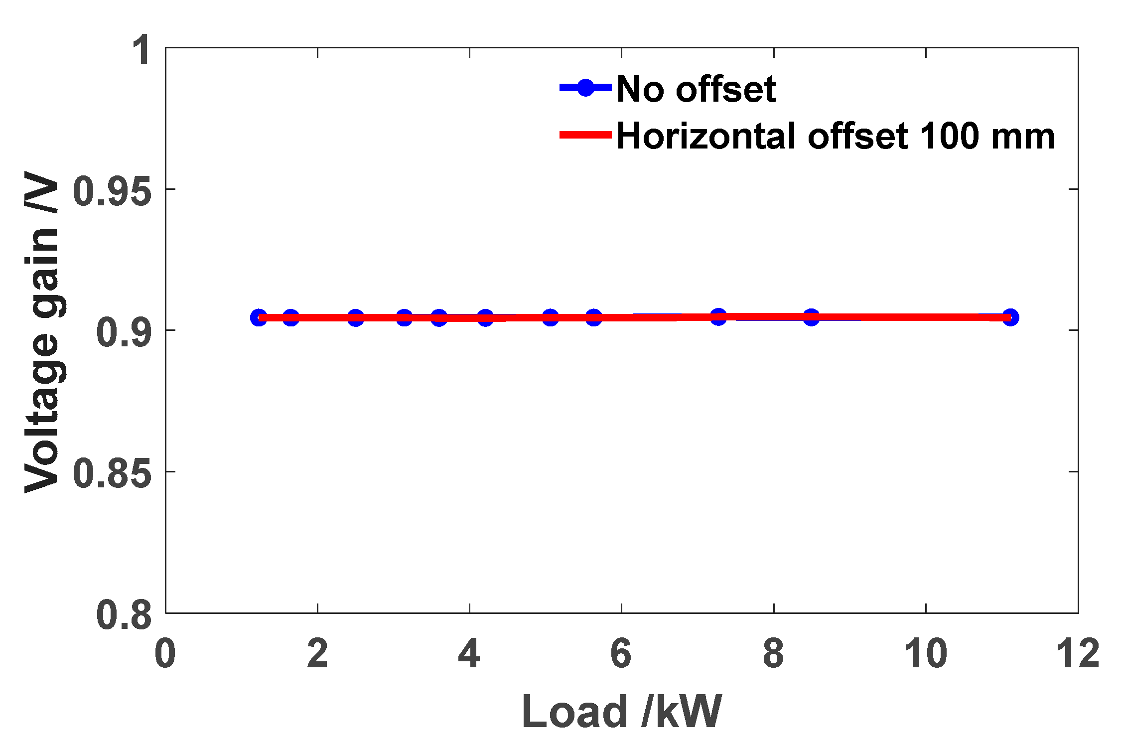
The plane offset distance of receiving and transmitting coil (mm)0–100
Table 2. Comparison of IPT systems with CVCC output characteristics.
Ref.TopologyPowerEfficiency
[10]LCC-S + Uncontrolled rectifier3.3 kW89.2%
[11]DLCC + Uncontrolled rectifier3.3 kW92.9%
[12]LCC-S + DLCC + Uncontrolled rectifier0.12 kW92.2%
[26]LCC-S + Uncontrolled rectifier + Boost Converter0.5 kW92.9%
[29]DLCC + Semi-synchronous rectifier2.5 kW88%
This workDLCC + Controllable synchronous rectifier11 kW95.6%
Disclaimer/Publisher’s Note: The statements, opinions and data contained in all publications are solely those of the individual author(s) and contributor(s) and not of MDPI and/or the editor(s). MDPI and/or the editor(s) disclaim responsibility for any injury to people or property resulting from any ideas, methods, instructions or products referred to in the content.

