
Modulation of Diamond PN Junction Diode with Double-Layered n-Type Diamond by Using TCAD Simulation
by
 and
and
Caoyuan Mu
1,2,†,
Genzhuang Li
1,2,†,
Xianyi Lv
1,2,
Qiliang Wang
1,2,
Hongdong Li
1,
Liuan Li
1,2,* and
Guangtian Zou
1,2,* 1
State Key Laboratory of Superhard Materials, Jilin University, Changchun 130015, China
2
Shenzhen Research Institute, Jilin University, Shenzhen 518057, China
*
Authors to whom correspondence should be addressed.
†
These authors contributed equally to this work.
Electronics 2024, 13(9), 1703; https://doi.org/10.3390/electronics13091703
Submission received: 13 March 2024
/
Revised: 23 April 2024
/
Accepted: 24 April 2024
/
Published: 28 April 2024
(This article belongs to the Special Issue Recent Advances in Wide Bandgap Semiconductors)
Abstract
:This study proposed a novel double-layer junction termination structure for vertical diamond-based PN junction diodes (PND). The effects of the geometry and doping concentration of the junction termination structure on the PNDs’ electrical properties are investigated using Silvaco TCAD software (Version 5.0.10.R). It demonstrates that the electric performances of PND with a single n-type diamond layer are sensitive to the doping concentration and electrode location of the n-type diamond. To further suppress the electric field crowding and obtain a better balance between breakdown voltage and on-resistance, a double-layer junction termination structure is introduced and evaluated, yielding significantly improved electronic performances. Those results provide some useful thoughts for the design of vertical diamond PND devices.
1. Introduction
Energy consumption worldwide has become an increasingly serious problem with the booming of industry and economy. Si-based devices are currently the most widely used power devices in electrical applications. However, further improvement in the energy efficiency of Si-based power devices through device design and manufacture is a challenge due to the theoretical limits of the material [1,2,3]. Wide band gap materials such as diamond, Ga2O3, and GaN have been used in recent years for the design and fabrication of power devices because their excellent physical properties meet the growing efficiency requirements [4,5,6,7,8,9]. Diamond possesses an ultrawideband gap, high thermal conductivity, and high electric field, high carrier mobility [10,11,12], making it the most suitable material for high-power, high-temperature, high-voltage, and high-frequency power electronics applications [13,14,15].
However, the industrialization of diamond devices still faces the following key technical issues that need to be resolved: (1) the epitaxial growth of large-size single-crystal diamond wafers; (2) the preparation of high-quality and low-defect diamond wafers; (3) high efficiency and controllable n-type and p-type doping technologies; and (4) the advanced structure of power devices. First of all, increasing the wafer size can theoretically reduce the material loss caused by the production process (such as chip cutting), thus improving the utilization ratio. At the same time, the larger wafer size improves production efficiency, reduces cost, and improves yields. The single crystal size of natural diamond or high-pressure high-temperature growth is usually less than 15 mm. Recently, 1-inch, 2-inch, and 4-inch diamond wafers have been obtained through 3D homoepitaxial growth, mosaic technique, and heteroepitaxy technique, respectively [16]. Secondly, dislocation and defect density are two key factors of power semiconductor materials, especially for the high-power vertical device because the current conduction direction parallels the dislocation. Generally, the yield of power chips shows an exponential decrease with the defect density. Also, many kinds of methods (growth parameters modulation, dislocation filter layer, epitaxial lateral overgrowth, etc.), have been developed to enhance the crystalline quality of diamond wafers [17,18].
So far, diamond-based rectifiers, e.g., Schottky barrier diodes (SBDs) have become a hot research topic [19,20]. The vertical diamond SBD with the high breakdown electric field (5.38 MV/cm) was prepared by Wang et al. using a field plate-assisted termination structure [21]. The highest current density (>60 kA/cm2 at 6 V) was also reported by Makino et al. with an SPND to balance the on-resistance (Ron) and the breakdown voltage (Vbd) [22]. Furthermore, Shikata et al. confirmed the high-temperature stability of diamond SBD at 500 °C for a long work period [23]. Previous works demonstrate that the PND can provide a lower reverse leakage current, better avalanche capability, and better surge current capability than that of the SBD [24]. Also, the PN junction is usually adopted as the termination structure for SBDs. We previously proposed a novel beveled PN junction termination structure for the vertical diamond SBD, in which the Schottky contact is also located in the (100) p-type diamond while the PND is formed on the beveled (110) plane [20]. It demonstrates that the forward turn-on voltage (Von) of the device is almost unchanged compared with that of conventional SBD. However, the depletion region formed by the PN junction hinders the current conduction area and slightly increases Ron. Since the PN junction does not conduct and inject minority carriers under forward bias, the introduction of PN junction does not degrade the reverse recovery performance. In the reverse bias state, the depletion region of the PN junction significantly alleviates the electric field concentration phenomenon and enhances the Vbd. However, there are rare reports on the development of (100) diamond PN junction diodes (PNDs) and Schottky PN junction structure diodes (SPND) due to the challenge of realizing high-quality n-type doped diamonds. Generally, the n-type doped diamond with an effective dopant is still a challenge currently although there exist many promising elements such as Li and Na in group I, N and P in group V, and O and S in group VI [25,26,27]. Considering some key factors such as the donor activation energy, dopant solubility, doping efficiency, and reproducibility, phosphorus is regarded as the most promising dopant at present. However, the doping efficiency of phosphorus in diamond at room temperature is low (50–90% compensation rate) and the ionization energy of the donor level is relatively high (0.57 eV) [28]. In addition, the hydrogen atoms in the growth atmosphere of diamond produce a passivation effect, which inhibits the ionization of phosphorus and leads to high resistivity. Finally, the doping concentration and doping efficiency on the (001) diamond are 1–2 orders of magnitude lower compared to the (113) and (111) facets. From the perspective of a power device, non- (001) -oriented diamond substrates still face problems such as small size, growth difficulty, and poor surface flatness [29]. Therefore, it requires an extremely high doping concentration to obtain the n-type (001) diamond with small resistance. On the other hand, the deteriorated crystalline quality of diamonds with high doping concentration results in the performance degradation of PNDs. Recently, a double-layer NiO was adopted to construct Ga2O3 heterojunction PNDs [30]. The relatively small hole concentration in the bottom NiO layer helps to enhance the Vbd while the high hole concentration in the top NiO is beneficial to obtain good contact and reduce the resistance.
Taking into account the challenge of high-quality n-type doped diamond, one possible route is to construct the heterojunction. In the wide-band semiconductor material system, there are some materials that are easy to realize n-type doping (with electron concentration of 1017–1019 cm−3) such as gallium oxide, gallium nitride, and zinc oxide. Therefore, these materials can also be employed instead of n-type diamonds to form heterojunctions to realize the JTE structure [20]. However, the heterojunction encounters the interface issue experimentally. Therefore, we believe that the double-layered structure is useful for improving the electrical properties of diamond PND. The first n−-diamond layer with relatively low doping concentration and high thickness provides a wider depletion region to sustain the reverse bias. In addition, the n−-diamond layer also shows better crystalline quality, which is beneficial to improve the heterojunction interface. On the other hand, the increase in doping concentration in the n+-diamond layer helps to modulate the electric field distribution and improve the contact with the electrode. However, the design and manufacture of diamond PND has been little mentioned in the past decades. In this paper, we proposed a vertical diamond PND with a double-layer n-type diamond. The Silvaco technology computer-aided design (TCAD) simulation was performed to investigate the influence of different parameters on the PND. The TCAD is usually adopted in developing new semiconductor devices and their electrical characteristics to reduce costly and time-consuming wafer testing. Based on basic physical equations such as diffusion and transport equations, the simulation approach guarantees predictive accuracy over a wide range of technologies. One of the key parameters to evaluate the performances of power devices is Baliga’s figure of merit (BFOM = Vbd2/Ron). The thickness, doping concentration, and relative location of the n-type diamond layer and the size of the electrode were studied to enhance the electric field distribution in PND, which is beneficial to balance the Ron and VBD.
2. Design Models and Calibration
The schematic cross-section of the diamond PNDs with single and double junction termination extensions designed by Silvaco TCAD software is shown in Figure 1a,b. The single layer junction termination structure PND (Figure 1a, named S-PND) is composed of a heavily doped diamond region (p+ diamond substrate, 1 μm with the hole concentration of 1 × 1019 cm−3 at 550 K), a lightly doped diamond drift region (p− diamond layer, 4 μm with the hole concentration of 1 × 1016 cm−3 at 550 K) and a single n-type diamond layer. The anode and cathode were set at the bottom of the p+ region and the top of the n-type region, respectively. Subsequently, we carried out the design of the PND with a double-layer n-diamond structure (Figure 1b, named D-PND). On the one hand, the double-layer structure can improve the interface quality of the PN junction. On the other hand, this structure serves as the junction termination extension (JTE), which was commonly introduced for the power diode. We use the Shockley–Read–Hall Recombination, Auger Recombination, Bandgap Narrowing, Low-Field Mobility, and Parallel Electric Field Dependence model for simulation [31]. The Shockley–Read–Hall (SRH) Recombination primarily describes phonon transitions that occur in the presence of a trap (or defect) within the forbidden gap of the semiconductor. This is essentially a two-step process, the theory of which was first derived by and then by Hall. The SRH is modeled as follows:
where n and p are the concentrations of electron and hole, respectively, nie is the intrinsic carrier concentration, Etrap is the difference between the trap energy level and the intrinsic Fermi level (default value), T is the lattice temperature in degrees Kelvin, and τp (2 × 10⁻⁹ in this work) and τn (2 × 10⁻⁹ in this work) are the electron and hole lifetimes, respectively.
Auger recombination occurs through a three-particle transition whereby a mobile carrier is either captured or emitted. Auger Recombination is commonly modeled using the expression:
where γe and γp are the Auger coefficients of electrons (default values) and holes (default values), respectively.
The low-field mobility model is adopted according to:
where T is the lattice temperature, μn (500 and 20 for p-type and n-type diamond in this work) and μp (200 and 1000 for p-type and n-type diamond in this work) are the mobility of electrons and holes at 300 K. θn (1.5 in this work) and θp (1.5 in this work) are the mobility of electrons and holes at 300 K.
Firstly, the S-PND was used to evaluate the effects of electrode size and n-type diamond doping concentration and depths. For the D-PND, the dimensions and doping concentration of the double-layer n-type diamond were used for the study. The device performance (in particular, forward conduction characteristics and reverse breakdown voltage) was simulated by using the models reported in our previous work [32]. The key material parameters of the diamond were set according to reference [33]. Generally, the incomplete ionization model is adopted to evaluate the temperature dependency of dopant ionization due to the large activation energy. When the temperature increases from 250 K to 650 K, the activation of dopants will be enhanced obviously to realize a small resistance. As discussed in our previous work [34], we think that 550 K is the suitable temperature used for simulation. It is worth noting that the critical electric field for a diamond is set to be 6 MV/cm, this is attributed to the fact that the impact ionization coefficient of a diamond is not yet fully understood.
3. Results and Discussions
3.1. Modulation of the Structure Parameters for the S-PND
Firstly, the effect of the cathode size (reflected as the distance between the cathode edge and the n-type diamond edge, S = 0, 1, 2, 3 μm in Figure 1a) on the electrical behavior of the S-PND was evaluated. For this simulation, the thickness and electron concentration of n-type diamond is set to 150 nm and 5 × 1017 cm−3 (at 550 K), respectively.
The electrical characteristics are summarized in Table 1 and shown in Figure 2. The results show that the Ron of the S-PNDs increases significantly from 4.51 mΩ·cm2 (S = 0 μm) to 7.04 mΩ·cm2 (S = 3 μm). These changes can be explained by the current density distributions at a forward bias of 8 V (Figure 3a,b). The current conduction area decreases with decreasing cathode size, which leads to an increase in Ron. On the other hand, the change in the size of the cathode has a positive effect on the electric field distributions of the S-PNDs. Figure 3c–f show the effect of the cathode size on the electric field distributions of S-PNDs at the reverse Vbd. With decreasing cathode size, new electric field peaks are generated at the cathode edge to relieve the electric field crowding around the JTE edge. It is worth noting that the electric field tends to balance between all the peaks when S = 2 μm, while it tends to concentrate around the electrode edge and leads to the degradation of the device performance when S = 3 μm. Therefore, the S-PND with S = 2 μm can obtain the appropriate Ron and Vbd to obtain the best BFOM value.
In addition, considering that the device performances of S-PNDs may be influenced by the parameters of JTE, different depths (D = 100, 150, 200 nm) and electron concentrations (1 × 10¹⁷, 5 × 10¹⁷, and 1 × 1018 cm−3 at 550 K) of n-type diamond were used to perform the evaluation together. The electrical characteristics of the S-PNDs are shown in Table 2 and Figure 4. It demonstrates that the S-PND with D = 150 nm and electron concentration of 5 × 1017 cm−3 can simultaneously obtain a larger Vbd and a smaller Ron, resulting in the highest BFOM value. For the S-PND with a 100 nm n-type diamond layer, the n-type diamond layer is rapidly depleted and severe electric field crowding occurs at the cathode edge (Figure 4a). However, when the n-type diamond layer thickness increases to 200 nm, the controllability of the cathode electrode becomes weak, and the electric field tends to concentrate at the n-type diamond edge (Figure 4b). The uneven electric field distribution results in the rapid breakdown of S-PND. When the electron concentration of n-type diamond is relatively low (1 × 1017 cm−3), the n-type diamond can be depleted easily. The electric field tends to accumulate at the electrode edge, causing premature breakdown of the device (Figure 4c). On the other hand, the electric field tends to concentrate at the n-type diamond layer edge when the electron concentration reaches 1 × 1018 cm−3, which also degrades the electrical performance (Figure 4d).
3.2. The Effects of Structure Parameters on the D-PND
Based on the above result, the performance of the PND is mainly influenced by the parameters of the n-type diamond layer. Therefore, we designed a double-layer structure PND (D-PND), consisting of n+-diamond layer and n−-diamond layer, to further improve the performances. The investigation of the performances of D-PND is carried out by first adjusting the relative distance (S1 in Figure 1b) between the n+-diamond layer and the n−-diamond layer. The electrode length is fixed at 9 μm, and the thicknesses of the n−-diamond layer and n+-diamond layer are set to 100 nm and 50 nm, respectively. The electron concentrations of the n−- and n+-diamond layer at 550 K are chosen to be 5 × 1017 cm−3 and 1 × 1018 cm−3, respectively. The simulated results are summarized in Table 3 and shown in Figure 5. In Figure 5e, we can see that the variation in S1 length presents no obvious effects on the forward performance of D-PND with the comparable Ron (Table 3), while the Vbd of D-PNDs is significantly influenced. These changes can be explained by the electric field distributions under Vbd (Figure 5). With the increase in S1, new electric field peaks are generated at the edges of the electrode and n+-diamond layer to relieve the electric field crowding in the PN contact region (Figure 5a,b). The D-PND with S1 = 1 μm achieves optimal performance through the balance between three electric field peaks (Figure 5c). However, the electric field peaks around the electrode edge and n+-diamond edge tend to merge together with further increasing S1, resulting in uneven electric field distribution and lower device performance (Figure 5d).
Subsequently, different doping concentrations of the double layers were used to modulate the performances of D-PNDs. The simulated electrical properties are summarized in Table 4, in which the doping concentrations of the double layers have a significant effect on the Ron and Vbd of the D-PNDs. Figure 6 provides some typical electric field distributions of the D-PNDs with different doping concentrations. Observed from Figure 6a, the n-type diamond layers are depleted totally and result in the electric field crowding around the cathode edge when the doping concentration of the n+-diamond layer and n−-diamond layer is low (5 × 1017 cm−3 and 1 × 1017 cm−3, respectively). As the doping concentration of the n+-diamond layer increases to 1 × 1018 cm−3 and that of the n− diamond layer increases to 5 × 1017 cm−3 (Figure 5b), the electric field distribution of the D-PND becomes uniform, leading to the highest Vbd and BFOM values. However, when the doping concentration of the n+ diamond layer was increased to 5 × 1018 cm−3 (Figure 6b), the crowding of the electric field tended to occur at the edges of the n+-layer and decreased the performance of the device. Therefore, the best performance of D-PND is achieved when the doping concentrations of the n+-and n− diamond layers are 1 × 1018 cm−3 and 5 × 1017 cm−3, respectively.
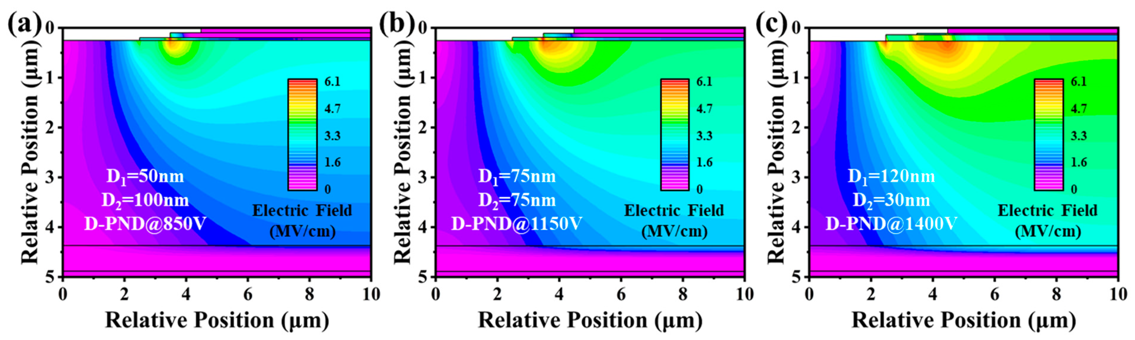
Finally, the total depth of the junction termination structure was controlled to 150 nm, and the D-PNDs were modulated using different n+ and n− diamond layer thicknesses (Table 5 and Figure 7). The results show that the electric field distributions of D-PNDs become uniform with the increasing n−-diamond layer thickness (D1) when the thickness is less than 100 nm. For the D-PND with D1 = 50 nm, and D2 = 100 nm (Figure 7a), the electric field tends to crowd at the edge of the n+-layer. For the D-PND with D1 = 75 nm, and D2 = 75 nm (Figure 7b), a new electric field peak appears at the n-diamond edger, which has a positive effect on alleviating the electric field crowding. For the D-PND with D1 = 100 nm, D2 = 50 nm (Figure 5b), the simultaneous presence of three electric field peaks at the electrode edge, the n+-diamond edge and the n−-diamond edge equalizes the electric field distribution inside the D-PND, which is conducive to obtaining excellent Vbd. However, further increasing D1 to larger than 100 nm, the electric field of the D-PNDs crowds at the edges of the PN junction contact (Figure 7c, with D1 = 120 nm, D2 = 30 nm) and degrade device performance.
4. Conclusions
In summary, we report a novel diamond PND with a double-layer JTE structure and comprehensively discuss the effects of different parameters on the electrical properties of the diamond D-PND. The simulation results demonstrate that the electric performances of PND with a single n-type diamond layer are sensitive to the doping concentration and electrode location of the n-type diamond, implying the necessity of a double-layer n-type diamond. The introduction of the double JTE structure has a positive effect on regulating the Ron and electric field distribution of the PND, and the BFOM value is significantly increased from 0.035 GW/cm2 to 0.414 GW/cm2. We believe that the results are very promising to facilitate the application of diamond PNDs for high-power and high-efficiency power electronics.
Author Contributions
Conceptualization, C.M.; methodology, G.L.; formal analysis, X.L.; validation: Q.W. and H.L.; writing—original draft preparation, C.M. and G.L.; supervision, L.L.; funding acquisition, L.L. and G.Z. All authors have read and agreed to the published version of the manuscript.
Funding
This work is supported by the Natural Science Foundation of Jilin Province (No. 20240101313JC), Open Project of State Key Laboratory of Superhard Materials, Jilin University (No. 202314) and Development Program of the Ministry of Industry and Information Technology (No. 23CYJCZZ164).
Data Availability Statement
Data are contained within the article.
Acknowledgments
The authors thank T. T. Wang from Xidian University for the guidance and fruitful discussions on simulation.
Conflicts of Interest
The authors declare no conflicts of interest.
References
- Hower, P.L.; Pendharkar, S.; Efland, T. Current status and future trends in silicon power devices. In Proceedings of the 2010 International Electron Devices Meeting, San Francisco, CA, USA, 6–8 December 2010; pp. 13.11.11–13.11.14. [Google Scholar]
- Millán, J.; Godignon, P.; Perpiñà, X.; Pérez-Tomás, A.; Rebollo, J. A Survey of Wide Bandgap Power Semiconductor Devices. IEEE Trans. Power Electron. 2014, 29, 2155–2163. [Google Scholar] [CrossRef]
- Zhang, Y.; Dadgar, A.; Palacios, T. Gallium nitride vertical power devices on foreign substrates: A review and outlook. J. Phys. D Appl. Phys. 2018, 51, 273001. [Google Scholar] [CrossRef]
- Yang, H.; Ma, Y.; Dai, Y. Progress of structural and electronic properties of diamond: A mini review. Funct. Diam. 2022, 1, 150–159. [Google Scholar] [CrossRef]
- Zhang, X.; Liao, F.; Huang, X.; Yao, D.; Du, Z.; Ma, X.; Chen, Y.; Liu, J. Design of a 6 kV Beta-Ga2O3 PN Heterojunction Diode with Etched Double-Layered NiO with a Figure of Merit of 10 GW cm−2. ECS J. Solid State Sci. Technol. 2022, 11, 045012. [Google Scholar] [CrossRef]
- Umezawa, H. Recent advances in diamond power semiconductor devices. Mater. Sci. Semicond. Process. 2018, 78, 147–156. [Google Scholar] [CrossRef]
- Zhang, J.; Dong, P.; Dang, K.; Zhang, Y.; Yan, Q.; Xiang, H.; Su, J.; Liu, Z.; Si, M.; Gao, J.; et al. Ultra-wide bandgap semiconductor Ga2O3 power diodes. Nat. Commun. 2022, 13, 3900. [Google Scholar] [CrossRef] [PubMed]
- Ma, S.; Kumaresan, Y.; Dahiya, A.S.; Lorenzelli, L.; Dahiya, R.S. Flexible Tactile Sensors Using AlN and MOSFETs Based Ultra-Thin Chips. IEEE Sens. J. 2023, 23, 23988–23994. [Google Scholar] [CrossRef]
- Maeda, T.; Page, R.; Nomoto, K.; Toita, M.; Xing, H.G.; Jena, D. AlN quasi-vertical Schottky barrier diode on AlN bulk substrate using Al0.9Ga0.1N current spreading layer. Appl. Phys. Express 2022, 15, 061007. [Google Scholar] [CrossRef]
- Amaratunga, G.A.J. A Dawn for Carbon Electronics? Science 2002, 297, 1657–1658. [Google Scholar] [CrossRef]
- Isberg, J.; Hammersberg, J.; Johansson, E.; Wikström, T.; Twitchen, D.J.; Whitehead, A.J.; Coe, S.E.; Scarsbrook, G.A. High Carrier Mobility in Single-Crystal Plasma-Deposited Diamond. Science 2002, 297, 1670–1672. [Google Scholar] [CrossRef]
- Inyushkin, A.V.; Taldenkov, A.N.; Ralchenko, V.G.; Bolshakov, A.P.; Koliadin, A.V.; Katrusha, A.N. Thermal conductivity of high purity synthetic single crystal diamonds. Phys. Rev. B 2018, 97, 144305. [Google Scholar] [CrossRef]
- Shimaoka, T.; Koizumi, S.; Kaneko, J.H. Recent progress in diamond radiation detectors. Funct. Diam. 2022, 1, 205–220. [Google Scholar] [CrossRef]
- Twitchen, D.J.; Whitehead, A.J.; Coe, S.E.; Isberg, J.; Hammersberg, J.; Wikstrom, T.; Johansson, E. High-voltage single-crystal diamond diodes. IEEE Trans. Electron Devices 2004, 51, 826–828. [Google Scholar] [CrossRef]
- Umezawa, H.; Nagase, M.; Kato, Y.; Shikata, S.-i. High temperature application of diamond power device. Diam. Relat. Mater. 2012, 24, 201–205. [Google Scholar] [CrossRef]
- Li, G.; Li, D.; Mu, C.; Wang, Q.; Lv, X.; Li, L.; Zou, G. Effect of step-flow modulation on the large-size single crystal diamond through mosaic growth. Funct. Diam. 2023, 3, 2279057. [Google Scholar] [CrossRef]
- Xie, W.-L.; Lv, X.-Y.; Wang, Q.-L.; Li, L.-A.; Zou, G.-T. Relationship between spatial position of seed and growth mode in single-crystal diamond grown with an enclosed-type holder. Chin. Phys. B 2022, 31, 108106. [Google Scholar] [CrossRef]
- Li, D.; Wang, Q.; Lv, X.; Li, L.; Zou, G. Reduction of dislocation density in single crystal diamond by Ni-assisted selective etching and CVD regrowth. J. Alloys Compd. 2023, 960, 170890. [Google Scholar] [CrossRef]
- Makino, T.; Tanimoto, S.; Hayashi, Y.; Kato, H.; Tokuda, N.; Ogura, M.; Takeuchi, D.; Oyama, K.; Ohashi, H.; Okushi, H.; et al. Diamond Schottky-pn diode with high forward current density and fast switching operation. Appl. Phys. Lett. 2009, 94, 262101. [Google Scholar] [CrossRef]
- Li, D.; Wang, T.; Lin, W.; Zhu, Y.; Wang, Q.; Lv, X.; Li, L.; Zou, G. Design of vertical diamond Schottky barrier diode with a novel beveled junction termination extension. Diam. Relat. Mater. 2022, 128, 109300. [Google Scholar] [CrossRef]
- Li, Q.; Wang, J.; Shao, G.; Chen, G.; He, S.; Zhang, Q.; Zhang, S.; Wang, R.; Fan, S.; Wang, H.X. Breakdown Voltage Enhancement of Vertical Diamond Schottky Barrier Diode with Annealing Method and AlO Field Plate Structure. IEEE Electron. Device Lett. 2022, 43, 1937–1940. [Google Scholar] [CrossRef]
- Makino, T.; Kato, H.; Tokuda, N.; Ogura, M.; Takeuchi, D.; Oyama, K.; Tanimoto, S.; Okushi, H.; Yamasaki, S. Diamond Schottky-pn diode without trade-off relationship between on-resistance and blocking voltage. Phys. Status Solidi a 2010, 207, 2105–2109. [Google Scholar] [CrossRef]
- Ikeda, K.; Umezawa, H.; Ramanujam, K.; Shikata, S.-i. Thermally Stable Schottky Barrier Diode by Ru/Diamond. Appl. Phys. Express 2009, 2, 011202. [Google Scholar] [CrossRef]
- Zhou, J.; He, L.; Li, X.; Pu, T.; Li, L.; Ao, J.-P. Vertical GaN Schottky barrier diodes with area-selectively deposited p-NiO guard ring termination structure. Superlattices Microstruct. 2021, 151, 106820. [Google Scholar] [CrossRef]
- Lombardi, E.B.; Mainwood, A. A first principles study of lithium, sodium and aluminum in diamond. Diam. Relat. Mater. 2008, 17, 1349–1352. [Google Scholar] [CrossRef]
- Hu, X.J.; Li, R.B.; Shen, H.S.; Dai, Y.B.; He, X.C. Electrical and structural properties of boron and phosphorus co-doped diamond films. Carbon 2004, 42, 1501–1506. [Google Scholar] [CrossRef]
- Gao, N.; Gao, L.L.; Yu, H.Y. First-principles study of N and S co-doping in diamond. Diam. Relat. Mater. 2023, 132, 109651. [Google Scholar] [CrossRef]
- Katayama-Yoshida, H.; Nishimatsu, T.; Yamamoto, T.; Orita, N. Codoping method for the fabrication of low-resistivity wide band-gap semiconductors in p-type GaN, p-type AlN and n-type diamond: Prediction versus experiment. J. Phys. -Condens. Matter 2001, 13, 8901–8914. [Google Scholar] [CrossRef]
- Pinault-Thaury, M.-A.; Temgoua, S.; Gillet, R.; Bensalah, H.; Stenger, I.; Jomard, F.; Issaoui, R.; Barjon, J. Phosphorus-doped (113) CVD diamond: A breakthrough towards bipolar diamond devices. Appl. Phys. Lett. 2019, 114, 112106. [Google Scholar] [CrossRef]
- Gong, H.H.; Chen, X.H.; Xu, Y.; Ren, F.-F.; Gu, S.L.; Ye, J.D. A 1.86-kV double-layered NiO/β-Ga2O3 vertical p–n heterojunction diode. Appl. Phys. Lett. 2020, 117, 022104. [Google Scholar] [CrossRef]
- Li, G.; Mu, C.; Lin, W.; Li, D.; Lv, X.; Wang, Q.; Li, L.; Zou, G. Simulation study of vertical diamond Schottky barrier diode with field plate assisted junction termination extension. Mater. Today Commun. 2023, 35, 105968. [Google Scholar] [CrossRef]
- Wang, Q.; Wang, T.; Pu, T.; Cheng, S.; Li, X.; Li, L.; Ao, J. Hybrid-anode structure designed for a high-performance quasi-vertical GaN Schottky barrier diode. Chin. Phys. B 2022, 31, 057702. [Google Scholar] [CrossRef]
- Miyata, K.; Nishimura, K.; Kobashi, K. Device simulation of submicrometer gate p+-i-p+ diamond transistors. IEEE Trans. Electron Devices 1995, 42, 2010–2014. [Google Scholar] [CrossRef]
- Cai, G.; Mu, C.; Li, J.; Li, L.; Cheng, S.; Wang, Q.; Han, X. Vertical Diamond p-n Junction Diode with Step Edge Termination Structure Designed by Simulation. Micromachines 2023, 14, 1667. [Google Scholar] [CrossRef] [PubMed]
Figure 1.
The schematic cross-section of the PND with single-layer n-diamond structure (S-PND) (a) and the PND with double-layered n-diamond structure (D-PND) (b).
Figure 1.
The schematic cross-section of the PND with single-layer n-diamond structure (S-PND) (a) and the PND with double-layered n-diamond structure (D-PND) (b).
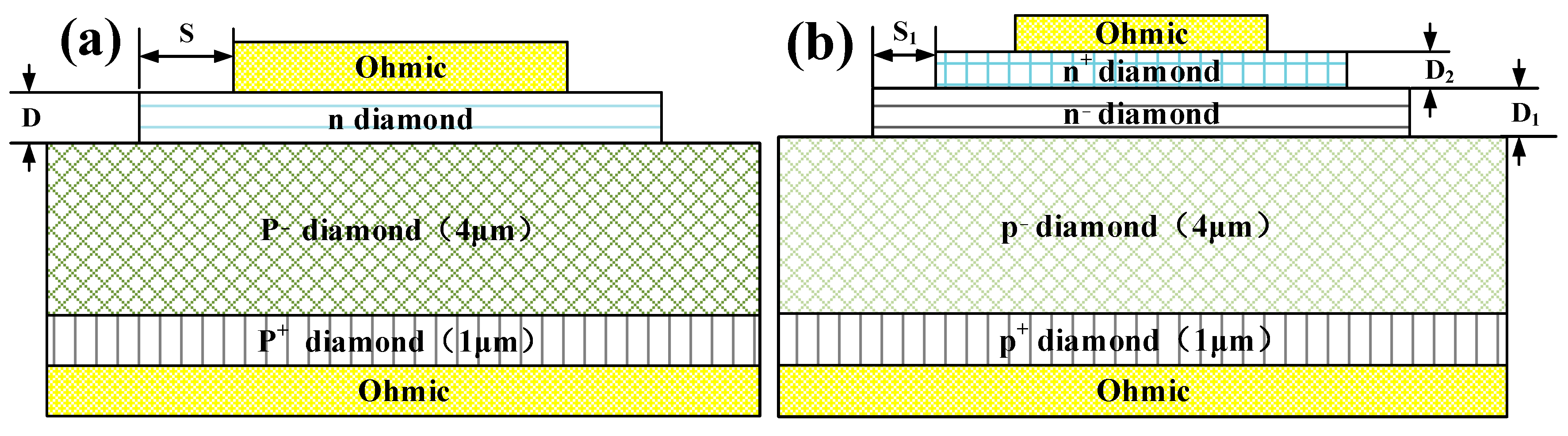
Figure 2.
The I–V curves and the corresponding Ron for the S-PNDs with different cathode sizes.
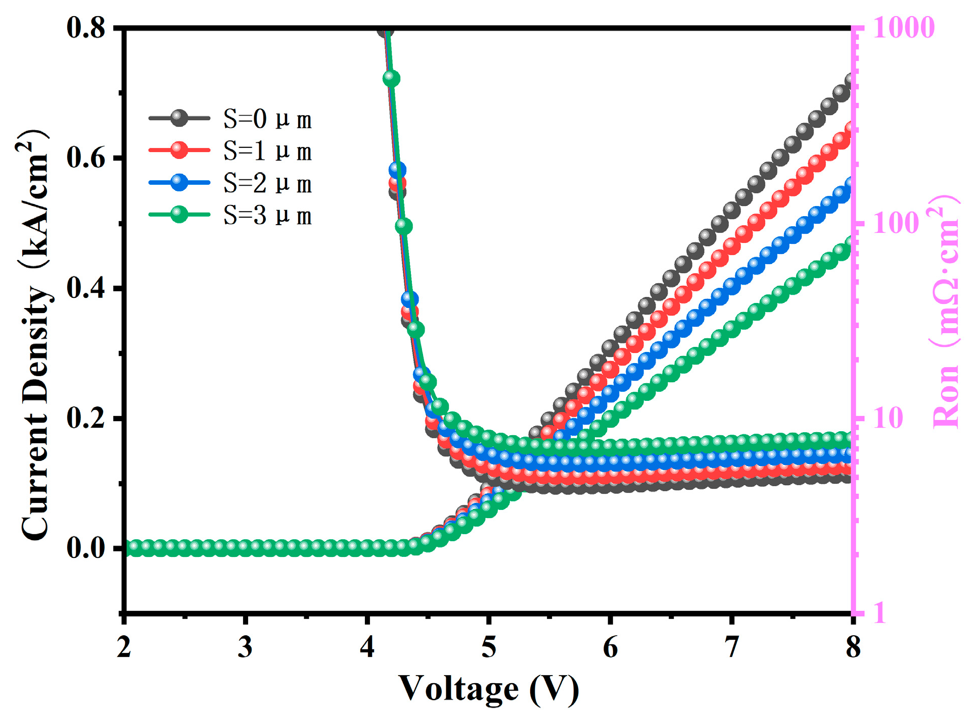
Figure 3.
(a,b) are the typical current distributions under forward bias (8 V) of S-PNDs with different cathode sizes. The typical electric field distributions under Vbd of S-PNDs are summarized in (c–f).
Figure 3.
(a,b) are the typical current distributions under forward bias (8 V) of S-PNDs with different cathode sizes. The typical electric field distributions under Vbd of S-PNDs are summarized in (c–f).
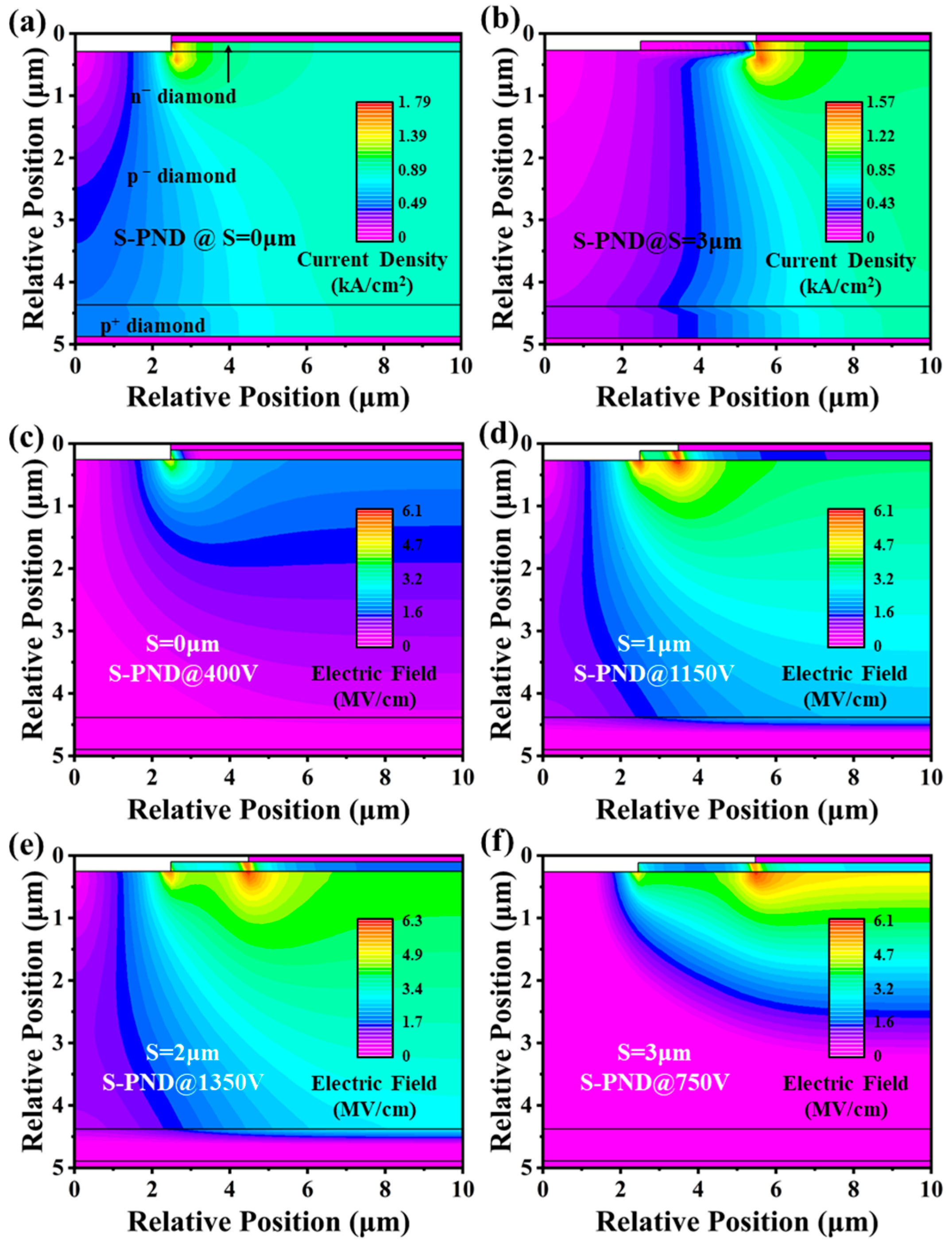
Figure 4.
The typical electric field distributions under Vbd of S-PNDs with different parameters of the n-type diamond layer, (a) D = 100 nm; (b) D = 200 nm; electron concentration are (c) 1017 cm−3 and (d) 1018 cm−3.
Figure 4.
The typical electric field distributions under Vbd of S-PNDs with different parameters of the n-type diamond layer, (a) D = 100 nm; (b) D = 200 nm; electron concentration are (c) 1017 cm−3 and (d) 1018 cm−3.
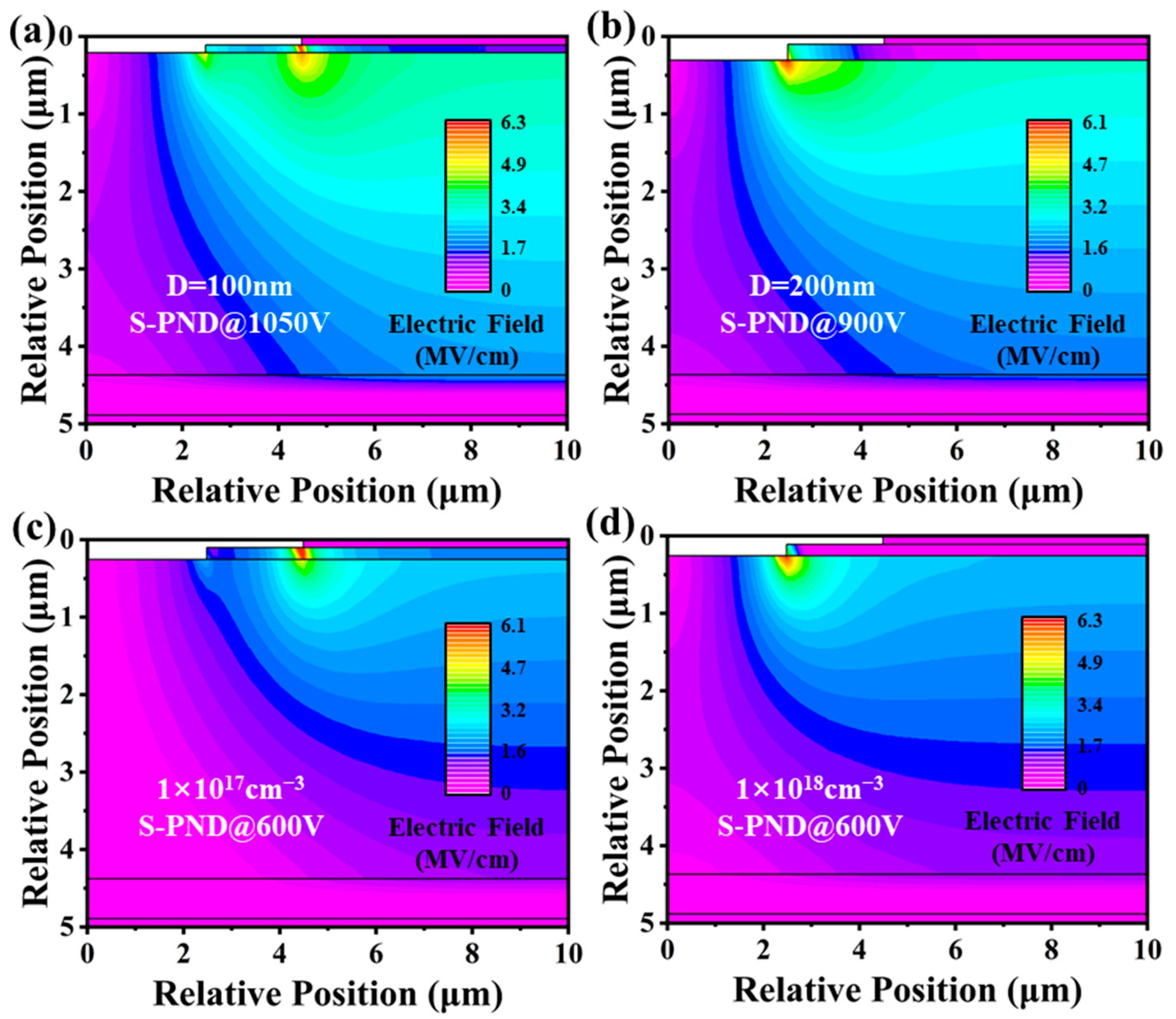
Figure 5.
(a–d) The electric field distributions under VBD of D-PNDs with different S1; (e) the I–V curves of D-PNDs with different S1 lengths.
Figure 5.
(a–d) The electric field distributions under VBD of D-PNDs with different S1; (e) the I–V curves of D-PNDs with different S1 lengths.
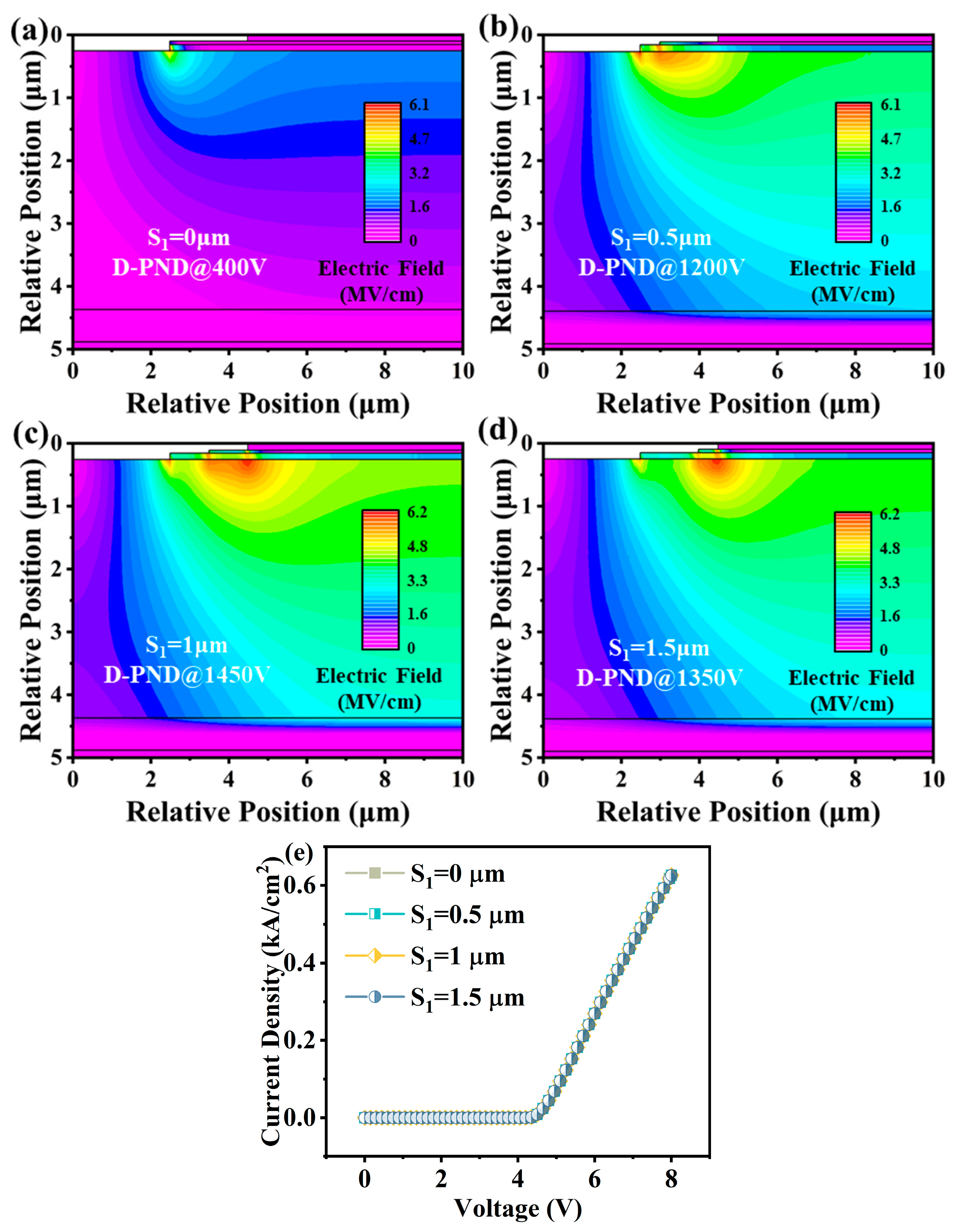
Figure 6.
The electric field distributions under Vbd of D-PNDs with different doping concentrations of n+ and n− diamond layer. (a) n− = 1017 cm−3, n+ = 5 × 1017 cm−3; (b) n− = 5 × 1017 cm−3, n+ = 5 × 1018 cm−3.
Figure 6.
The electric field distributions under Vbd of D-PNDs with different doping concentrations of n+ and n− diamond layer. (a) n− = 1017 cm−3, n+ = 5 × 1017 cm−3; (b) n− = 5 × 1017 cm−3, n+ = 5 × 1018 cm−3.
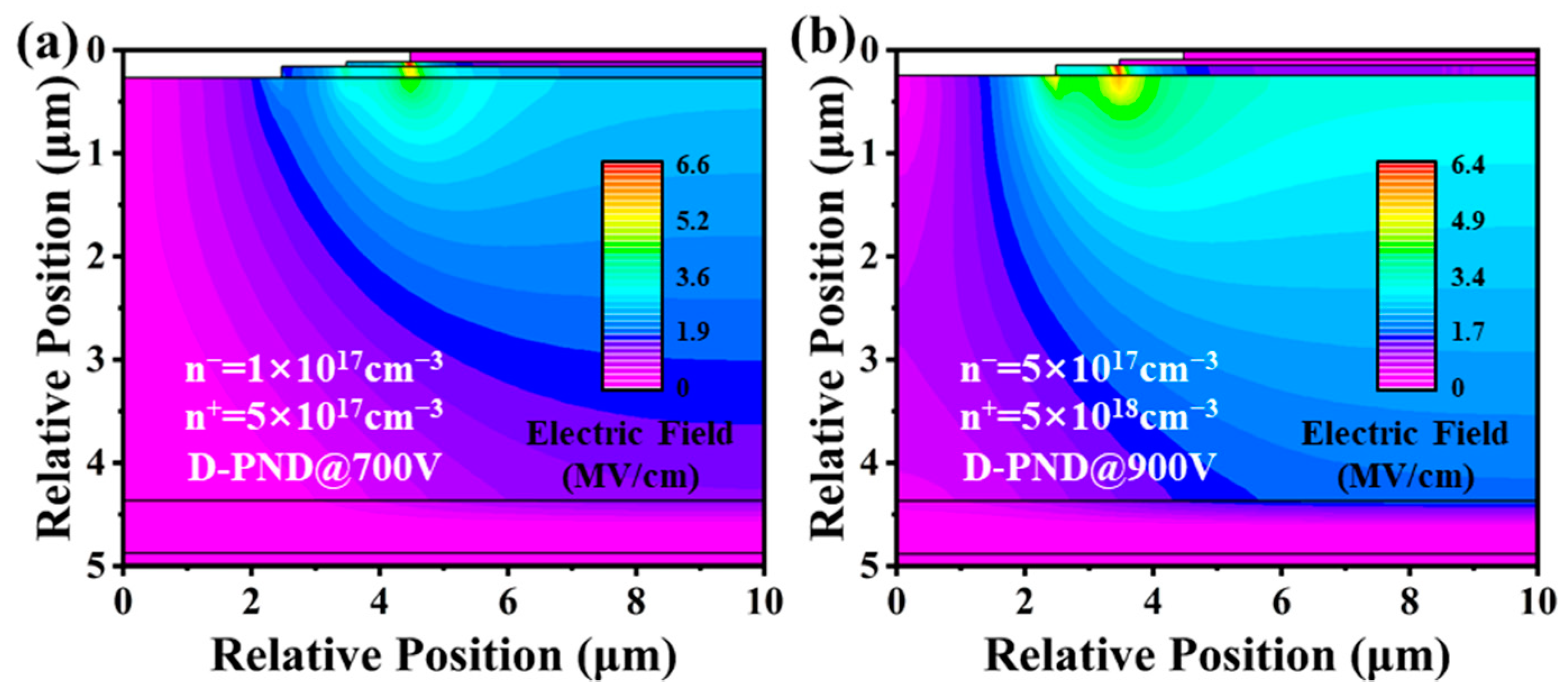
Figure 7.
The electric field distributions under VBD of D-PNDs with different n+ and n− diamond layer thicknesses. (a) D1 = 50 nm, D2 = 100 nm; (b) D1 = 75 nm, D2 = 75 nm; (c) D1 = 120 nm, D2 = 30 nm.
Figure 7.
The electric field distributions under VBD of D-PNDs with different n+ and n− diamond layer thicknesses. (a) D1 = 50 nm, D2 = 100 nm; (b) D1 = 75 nm, D2 = 75 nm; (c) D1 = 120 nm, D2 = 30 nm.

Table 1.
The simulated electric performances for the S-PNDs with different cathode sizes.
| S (μm) | Von (V) | Ron (mΩ·cm2) | Vbd (V) | BFOM (GW/cm2) |
|---|---|---|---|---|
| 0 | 5.7 | 4.51 | 400 | 0.04 |
| 1 | 5.7 | 5.06 | 1150 | 0.26 |
| 2 | 5.7 | 5.86 | 1350 | 0.31 |
| 3 | 5.7 | 7.04 | 750 | 0.08 |
Table 2.
The simulated electric performance for the S-PNDs with different parameters of the n-type diamond.
Table 2.
The simulated electric performance for the S-PNDs with different parameters of the n-type diamond.
| D (nm) | Electron Density (550 K) | Ron (mΩ·cm2) | Vbd (V) | BFOM (GW/cm2) |
|---|---|---|---|---|
| 100 | 5 × 1017 cm−3 | 5.32 | 1050 | 0.21 |
| 150 | 1 × 1017 cm−3 | 8.47 | 500 | 0.03 |
| 150 | 5 × 1017 cm−3 | 5.86 | 1350 | 0.31 |
| 150 | 1 × 1018 cm−3 | 4.52 | 600 | 0.08 |
| 200 | 5 × 1017 cm−3 | 6.52 | 900 | 0.13 |
Table 3.
The simulated electric performance for the D-PNDs with different S1.
| S1 (μm) | Ron (mΩ·cm2) | Vbd (V) | BFOM (GW/cm2) |
|---|---|---|---|
| 0 | 5.08 | 400 | 0.03 |
| 0.5 | 5.08 | 1200 | 0.28 |
| 1 | 5.08 | 1450 | 0.42 |
| 1.5 | 5.08 | 1350 | 0.36 |
Table 4.
The simulated electric performances for the D-PNDs with different doping concentrations of n+- and n−-diamond layers.
Table 4.
The simulated electric performances for the D-PNDs with different doping concentrations of n+- and n−-diamond layers.
| n− Electron Density (550 K) | n+ Electron Density (550 K) | Ron (mΩ·cm2) | Vbd (V) | BFOM (GW/cm2) |
|---|---|---|---|---|
| 1 × 1017 cm−3 | 5 × 1017 cm−3 | 6.76 | 700 | 0.07 |
| 1 × 1017 cm−3 | 1 × 1018 cm−3 | 6.07 | 1050 | 0.18 |
| 1 × 1017 cm−3 | 5 × 1018 cm−3 | 4.51 | 400 | 0.02 |
| 5 × 1017 cm−3 | 1 × 1018 cm−3 | 5.08 | 1450 | 0.42 |
| 5 × 1017 cm−3 | 5 × 1018 cm−3 | 3.56 | 900 | 0.23 |
| 1 × 1018 cm−3 | 5 × 1018 cm−3 | 3.06 | 500 | 0.08 |
Table 5.
The simulated electric performances for the D-PNDs with different n+-and n−-diamond layer thicknesses.
Table 5.
The simulated electric performances for the D-PNDs with different n+-and n−-diamond layer thicknesses.
| D1 (nm) | D2 (nm) | Ron (mΩ·cm2) | Vbd (V) | BFOM (GW/cm2) |
|---|---|---|---|---|
| 50 | 100 | 4.94 | 850 | 0.15 |
| 75 | 75 | 5.03 | 1150 | 0.26 |
| 100 | 50 | 5.08 | 1450 | 0.41 |
| 120 | 30 | 5.33 | 1400 | 0.37 |
Disclaimer/Publisher’s Note: The statements, opinions and data contained in all publications are solely those of the individual author(s) and contributor(s) and not of MDPI and/or the editor(s). MDPI and/or the editor(s) disclaim responsibility for any injury to people or property resulting from any ideas, methods, instructions or products referred to in the content. |
© 2024 by the authors. Licensee MDPI, Basel, Switzerland. This article is an open access article distributed under the terms and conditions of the Creative Commons Attribution (CC BY) license (https://creativecommons.org/licenses/by/4.0/).
Share and Cite
MDPI and ACS Style
Mu, C.; Li, G.; Lv, X.; Wang, Q.; Li, H.; Li, L.; Zou, G. Modulation of Diamond PN Junction Diode with Double-Layered n-Type Diamond by Using TCAD Simulation. Electronics 2024, 13, 1703. https://doi.org/10.3390/electronics13091703
AMA Style
Mu C, Li G, Lv X, Wang Q, Li H, Li L, Zou G. Modulation of Diamond PN Junction Diode with Double-Layered n-Type Diamond by Using TCAD Simulation. Electronics. 2024; 13(9):1703. https://doi.org/10.3390/electronics13091703
Chicago/Turabian StyleMu, Caoyuan, Genzhuang Li, Xianyi Lv, Qiliang Wang, Hongdong Li, Liuan Li, and Guangtian Zou. 2024. "Modulation of Diamond PN Junction Diode with Double-Layered n-Type Diamond by Using TCAD Simulation" Electronics 13, no. 9: 1703. https://doi.org/10.3390/electronics13091703
Note that from the first issue of 2016, this journal uses article numbers instead of page numbers. See further details here.