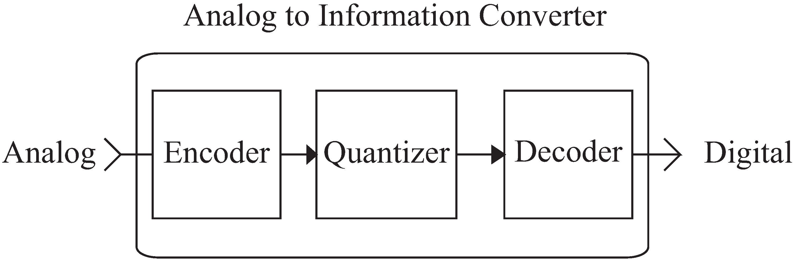
1. Introduction
Today, the vast majority of information processing takes place in the digital domain where computation on large scales has become increasingly cheap and convenient. Unfortunately, there are still many applications that struggle to take advantage of digital computation because the signals involved exceed the capabilities of current physical hardware approaches. Analog-to-digital converters (ADCs) are the traditional method for capturing real world signals and converting the information into digital samples. The two most critical measures of an ADC are its sampling speed, which limits the bandwidth of the signals it can accommodate, and the resolution, which limits the accuracy of the resulting samples. Conventional approaches process signals sequentially and different architectures trade sampling speed for resolution or
vice versa. This relationship is illustrated in [
1], where Walden analyzed the state-of-the-art in ADC technology in 1999, showing empirically that each additional bit in resolution decreases the sampling rate by a factor of two. Since then, these architectures have slowly increased in speed as fabrication processes have continued to improve according to Moore’s law, but the basic trend endures.
More recently, the field of compressed sensing (CS) [
2] has made a number of theoretical developments that leverage the structure of sparse signals into reduced sampling rates. One application where compressive sampling promises advances in the state-of-the-art is in the design of Analog to Information converters (A2I).
A typical A2I architecture consists of a front-end encoder and a back-end decoder with an analog to digital converter in between (see
Figure 1). The purpose of the coder is to transform the input signal into a representation that efficiently preserves information relevant to the function of the system. To achieve this, coders may be designed to exploit prior knowledge of the signals to be processed. Exploiting such prior knowledge has been employed in the design of hardware architectures for non-uniform amplitude [
3,
4] and spectral quantization [
5]. Modern communication systems also do this when high frequency signals are down-converted to base-band prior to low-rate sampling [
6].
Figure 1.
Analog to information converter architecture.
Figure 1.
Analog to information converter architecture.
Although related sampling theories, such as non-uniform sampling [
7], have also existed in the literature for many years, the CS framework has lead to the appearance of several novel sampling schemes. The modulated wideband converter (MWC) [
8,
9,
10] and the random demodulator (RD) [
11,
12,
13] are two of the earliest architectures. The compressive multiplexer (CMUX) [
14] is another more recent concept for hardware implementation. Each of these architectures achieves compressive sampling through some combination of parallelism, random modulation or sampling, and prior knowledge about the signals of interest. However, the assumptions on signal models and the details of the sampling process are different.
The RD architecture, described in [
13,
15], modulates the input signal with a random chipping sequence, and integrates the modulator output before digitizing with a conventional ADC. The practical details of implementing a RD architecture are described in [
12]. The RD operates on analog signals composed of sparse linear combinations of known basis functions. The random demodulator concept was demonstrated using discrete components in [
16]. Since the Nyquist rate requirement is satisfied by the high frequency contents of the chipping sequence, the ADC is allowed to operate at sub-Nyquist rates, and only the generation of the chipping sequences and the modulator require high speed hardware components. From a hardware perspective, compressive sampling is desirable because the modulation of the input signal with a binary sequence is simpler and easier to implement at high sampling rates as compared with the sample and hold circuits necessary for interleaved architectures. A single chip sub-Nyquist sampling receiver architecture operating between 100 MHz and 2 GHz was recently reported in the literature [
17,
18].
The MWC architecture modulates the input signal with multiple chipping sequences in parallel. The modulator output is low-pass filtered before being digitized by conventional ADCs. The MWC operates on analog signals that comply with the multi-band signal model described in [
8]. Note that the system modeling is primarily done in the frequency domain (whereas the RD is primarily modeled in the time domain). To the best of our knowledge it is also the only full scale system that has been realized in hardware using discrete components.
In order to process information in applications that require data conversion rates above the practical limits of traditional hardware, we need to consider alternative architectures. Parallel analog to digital converter architectures enable the design of high performance hardware systems in state-of-the-art CMOS technologies that can go beyond the bandwidth and resolution possible in single channel systems. Breaking the data conversion problem into multiple parallel sub-tasks is not a new concept, as exemplified by interleaved ADCs [
19] and other random sampling architectures [
20,
21], which have existed in the literature and in practice for many years. Interleaved ADCs operate multiple ADCs in parallel with offset sampling times such that the resulting low-rate samples can be multiplexed back together into a higher effective sampling rate [
22]. Although these architectures resolve the difficulty of designing fast ADCs, the high speed sample-and-hold circuits remain a challenge for high resolution Gsps ADCs.
No single ADC architecture can cover the whole design space. For instance, flash ADC architectures can produce a digitized sample with a non-iterative algorithm at high speeds. Unfortunately, they achieve this through massive parallelism that incurs an exponential cost in silicon real-estate, quickly limiting the achievable bits of resolution. On the other end of the spectrum, sigma-delta ADC architectures can produce high resolution samples using very little silicon area. However, it takes a relatively long time for the result to converge. Algorithmic ADC architectures often exhibit a more balanced tradeoff between bandwidth and resolution. Parallel data converter architectures look to harness the capabilities of multiple individual data converters to boost the overall system performance, generally by increasing the effective sampling rate while maintaining a resolution superior to that of the fastest flash architectures.
In this paper, we present a sampling architecture for compressed and Nyquist sampling [
23] and provide experimental results from a fabricated system in 0.5
CMOS technology. Even though we aim for reasonably high speed and resolution, our goal is to explore hardware CS sampling architecture ideas and hence our system is not fabricated in a state-of-the-art CMOS process. The coder (front end) architecture presented in this paper is inspired by both the RD and MWC schemes. We employ the concept of chipping and integrating from the RD, and the concept of multiple parallel channels from the MWC. The time domain modeling is also derived from the RD. The hardware combines multiple resources in parallel and is flexible enough to leverage additional signal structure, allowing information to be captured at a low data rate. The system is highly configurable and illustrates situations that mirror the behavior of interleaved ADC architectures as well as compressed sensing architectures.
2. Sampling Architecture
In the analog to information converter framework, signals are first processed in the analog domain before being quantized by analog to digital converters (ADC) [
20]. Additional signal processing in the digital domain may be required to recover the original input signal in a usable form. Such a situation occurs when analog signal processing is performed to optimize the performance of the analog to digital conversion.
Note that conventional data acquisition systems already follow this general framework in that they almost invariably perform simple transformations of the input signal, such as gain and offset correction or non-linear amplitude compression. These transformations are reversible in the sense that they can be undone with only knowledge of the transformation that was applied. However, irreversible transformations are also performed, the most common being low-pass filtering to satisfy the Nyquist criterion for the ADC.
In the specific implementation of our sampling architecture described herein, the analog coding consists in modulating the input signal with a high-speed chipping sequence and filtering the modulator output. The filter output is then digitized by the Nyquist ADC at a relatively low rate. When multiple parallel channels are used, each channel will normally use a different chipping sequence, so that the ADC outputs are not duplicated, unless some explicit redundancy is desired.
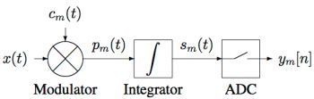
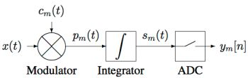
2.1. The Analog Processing Channel
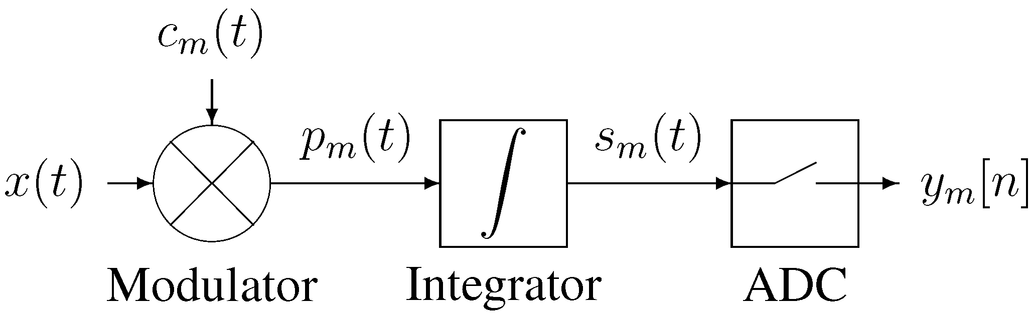
Our implementation of the analog processing channel is shown schematically in
Figure 2. The input signal
is multiplied with a digital chipping sequence
to produce a modulated signal
which in turn is integrated over a finite time period to produce the channel output signal
The channel output is sampled and digitized by the ADC, producing a digital sample
Figure 2.
Block diagram of the channel.
Figure 2.
Block diagram of the channel.
For an analog front-end using
M channels, the subscript
m refers to the channel index and takes values from the set
The integration period
is also the sampling period of the ADC, so we define the discrete time index
n such that
and hence
Since each chipping sequence
is a finite digital sequence, it is piecewise constant and can be described by a finite set of
N bits. The integration period
does not need to be the same as the chipping sequence length, but we do require that it be an integer multiple of
the duration of a chipping sequence bit. Additionally, since each integration period operates in essentially the same way, we can restrict our analysis to the first integration period (
) and let
without loss of generality. Therefore, let
where
takes values from the set
, and
indexes those values.
The modulator output is just the product of the input signal and the chipping sequence, so
Therefore, the output of a single integration period is
(As we are only considering the first integration period, we have dropped the discrete time index for simplicity.)
Since
is piecewise constant,
Equation 1 shows that the digitized samples can be broken down into a linear combination of the channel chipping sequence and short-term time integrations of the input signal
over the bit period
. If the duration of the bit is too long, any high-frequency components of the input signal will be lost or aliased. Therefore, the rate at which the chipping sequences alternate,
determines the effective input signal bandwidth that can be resolved by the system.
To simplify the expression for
we define the auxiliary discrete time signal
such that
and
We also define the vector notation of the bit sequence
and the set of samples
Now we can express the set of samples obtained from the front-end after the first integration period as:
where
.
If the duration of the bit is sufficiently short, then the input signal
can be reasonably approximated by the discrete time estimate
where
Recovery of the digitized input signal is therefore a matter of solving Equation 3 for z
2.2. System Configurations
The relationship between the output of a channel and the channel’s chipping sequence expressed in Equation 1 leads immediately to several interesting and instructive system configurations.
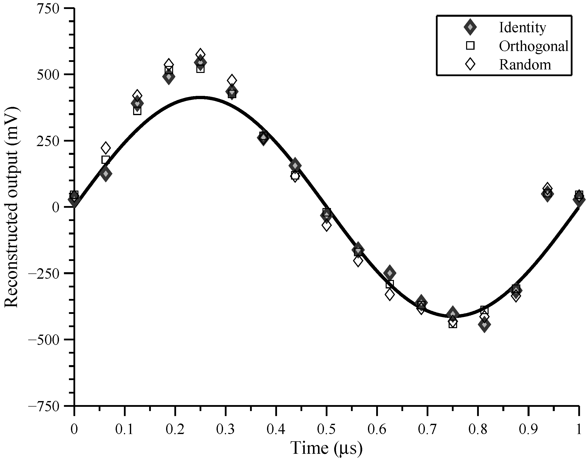
Case 1: If C is the identity matrix, then only one channel would be sampling the input during each bit period. If the chipping sequences were composed of 1’s and 0’s, then it would be easy to observe that the output of the mth channel is simply the integral of the ith bit period. Moreover, because the number of channels (M) is the same as the number of bit periods (N), when the parallel samples from the channels are interleaved in the right order, the original signal can be estimated. This is essentially how an interleaved ADC arrangement operates.
To get around the fact that we have arbitrarily restricted the composition of the chipping sequences to contain only
we can achieve the same effect by setting
Applying these chipping sequences to Equation 2 yields
where we have added and subtracted an additional
term to complete the summation over
N. As
in this case, the term
corresponds to the
chipping coefficient, while all other
, for
, are modified with a
coefficient. Solving for
yields,
where
Hence, although each ADC is only sampled at a rate of
, the effective sampling rate is
.
For other cases where
it is sufficient that
C be invertible, so that
can be recovered according to
Under these conditions, the chipping sequences form a basis set. Although
can be precomputed, so that the signal recovery requires only a matrix-vector multiplication, there is very little apparent advantage to this approach over the previous interleaving method.
Case 2: If the number of channels M is greater than the number of bits in the chipping sequence then Equation 3 is over-determined. A pseudo-inverse of is then needed to recover from but the pseudo-inverse can also be precomputed. The advantage of this approach is that the added redundancy may improve the robustness of the system.
Case 3: In general, this corresponds to an under-determined system and we would not be able to recover
uniquely. In this setting,
can still be recovered if additional information about the input signal is known. For example, if
meets appropriate sparse structure assumptions, then we can use pseudo-random chipping sequences, and the situation reduces to the well studied
optimization problem addressed in [
2,
12].
2.3. System Extensions
In practice, the chipping sequences are periodic so that they can be stored in a finite amount of space in a digital controller. However, the chipping sequence period can be different from the integration period so that changes from one integration interval to the next. All that is required for reconstruction of the signal in a given integration interval is for the of that integration interval to be known to the digital controller.
Note that both and must be integer multiples of the bit period and that the chipping sequence is also periodic in etc. Therefore, without loss of generality, we can redefine the chipping sequence period such that for some integer where k is the number of distinct versions of
Thus far we have assumed that the signal in a given time interval is reconstructed solely from the ADC outputs of a single integration interval. However, for some applications, it may be advantageous to reconstruct the signal using the ADC outputs from several (e.g., k) integration intervals. For instance, suppose that the input signal is known to be periodic in Then, the M chipping sequences can be applied by a single channel sequentially over M integration intervals, and the same set of M ADC outputs needed for reconstruction will be obtained but with a substantially reduced amount of hardware.
In general, we can reduce the number of channels by concatenating chipping sequences over several integration intervals and using the ADC outputs from these integration intervals in the reconstruction. However, the properties of the signal must not change substantially over these integration intervals, and the reconstruction algorithm must take into account the time shift between ADC outputs obtained from different integration intervals. This allows the reduction of the physical complexity of the sampling architecture at the cost of constraining how quickly the input signal characteristics are permitted to evolve in time.
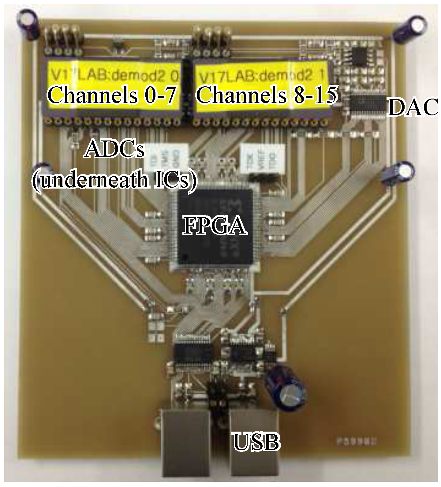
3. Analog Hardware Implementation
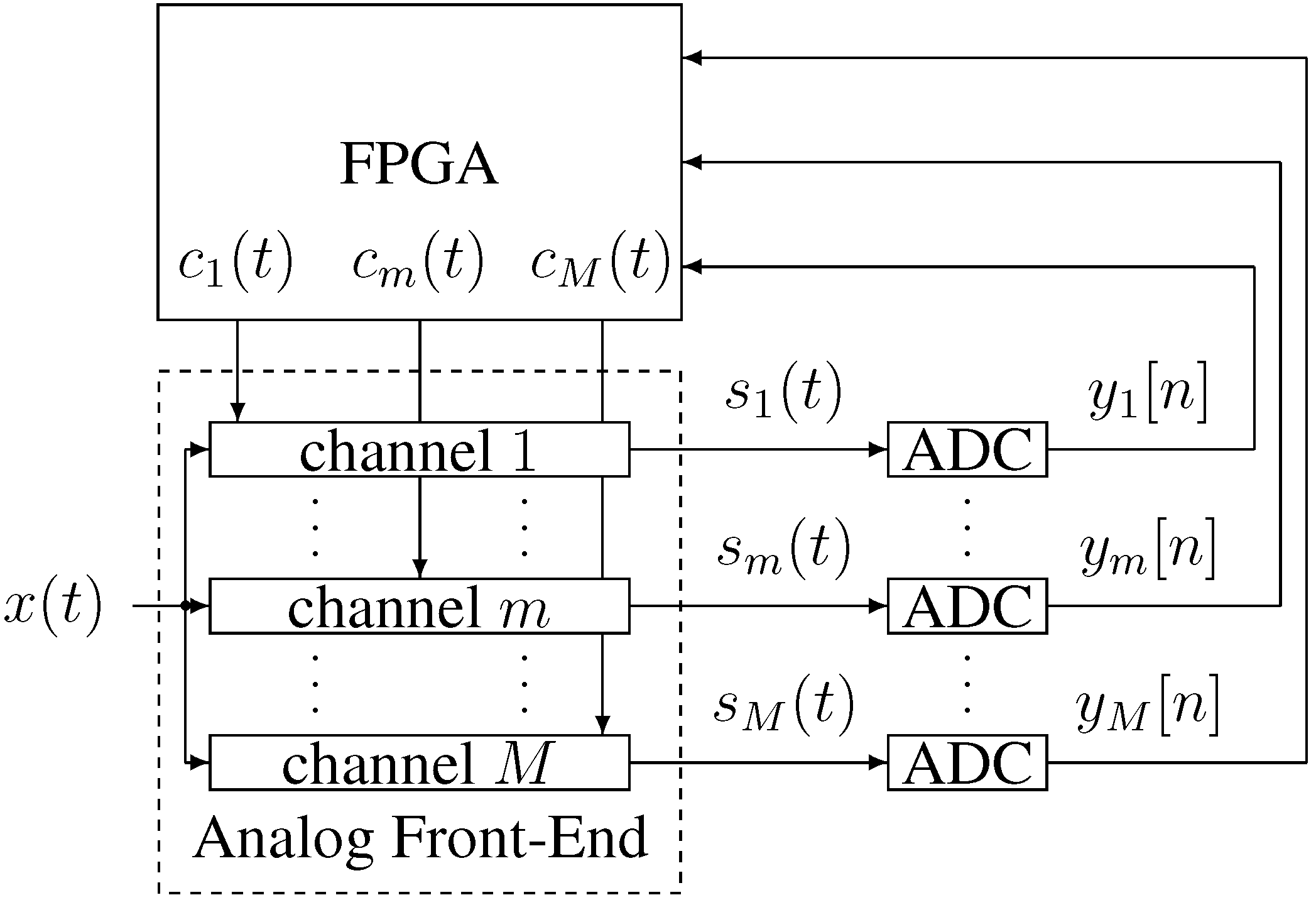
A complete sampling system can be built with discrete components, using discrete ADCs and a field programmable gate array (FPGA) to implement the digital control and chipping sequence generation, as shown in
Figure 3. The problem with this approach is that the analog front-end channels require many components to implement them with discrete parts.
To address this problem, we have designed and fabricated an analog front-end custom integrated circuit in a 0.5
CMOS process. The chip contains all the analog front-end components except for the ADCs (which we plan to integrate in future versions). The front-end was designed to operate from 20 kHz up to 200
The current design has 8 channels, but multiple chips can be operated in parallel for cases where
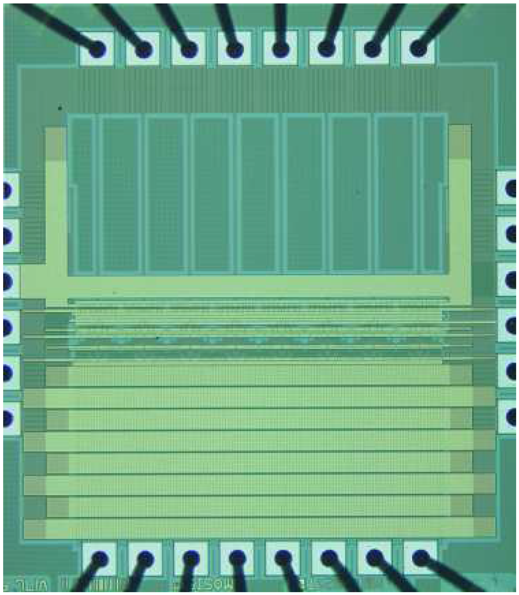
A micrograph of the fabricated chip is shown in
Figure 4. The active chip area is 0.66
(the remaining area is consumed by the I/O pads, wiring and fill).
Figure 3.
System block diagram.
Figure 3.
System block diagram.
Figure 4.
A micrograph of the fabricated mm × mm chip.
Figure 4.
A micrograph of the fabricated mm × mm chip.
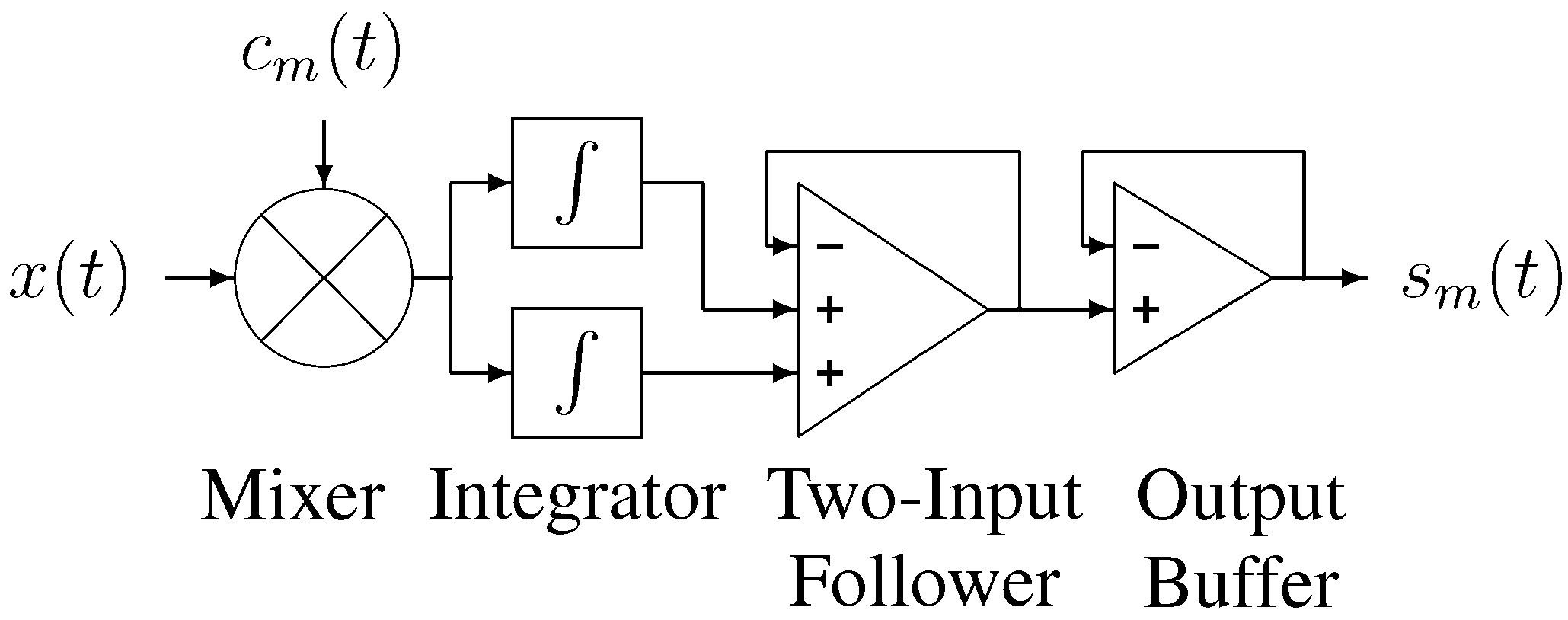
3.1. Channel Pipeline
The proper operation of the front-end requires that the integration periods follow one another without interruption. In practice the integration time interval needs to be followed by a hold interval to allow the ADC’s sampling circuit to acquire the integrator’s output, and then a reset interval to reset the integrator to its starting value. The hold interval in particular can be quite long, because commercial ADCs normally include track-and-hold circuits whose performance is on par with the conversion circuits.
We therefore designed our front-end channel using two integrators operating in tandem. While one integrator is integrating the input signal, the other is holding its value for the external ADC. Each integrator is reset just prior to switching back to integration mode, so that the sum of the reset interval and the hold interval is equal to the integration interval. This allows the output of one of the integrators to be available to the external ADC for almost a full integration period. A two-input voltage follower is used to select which integrator output is sent to the ADC. This arrangement is shown schematically in
Figure 5.
Figure 5.
Channel component block diagram.
Figure 5.
Channel component block diagram.
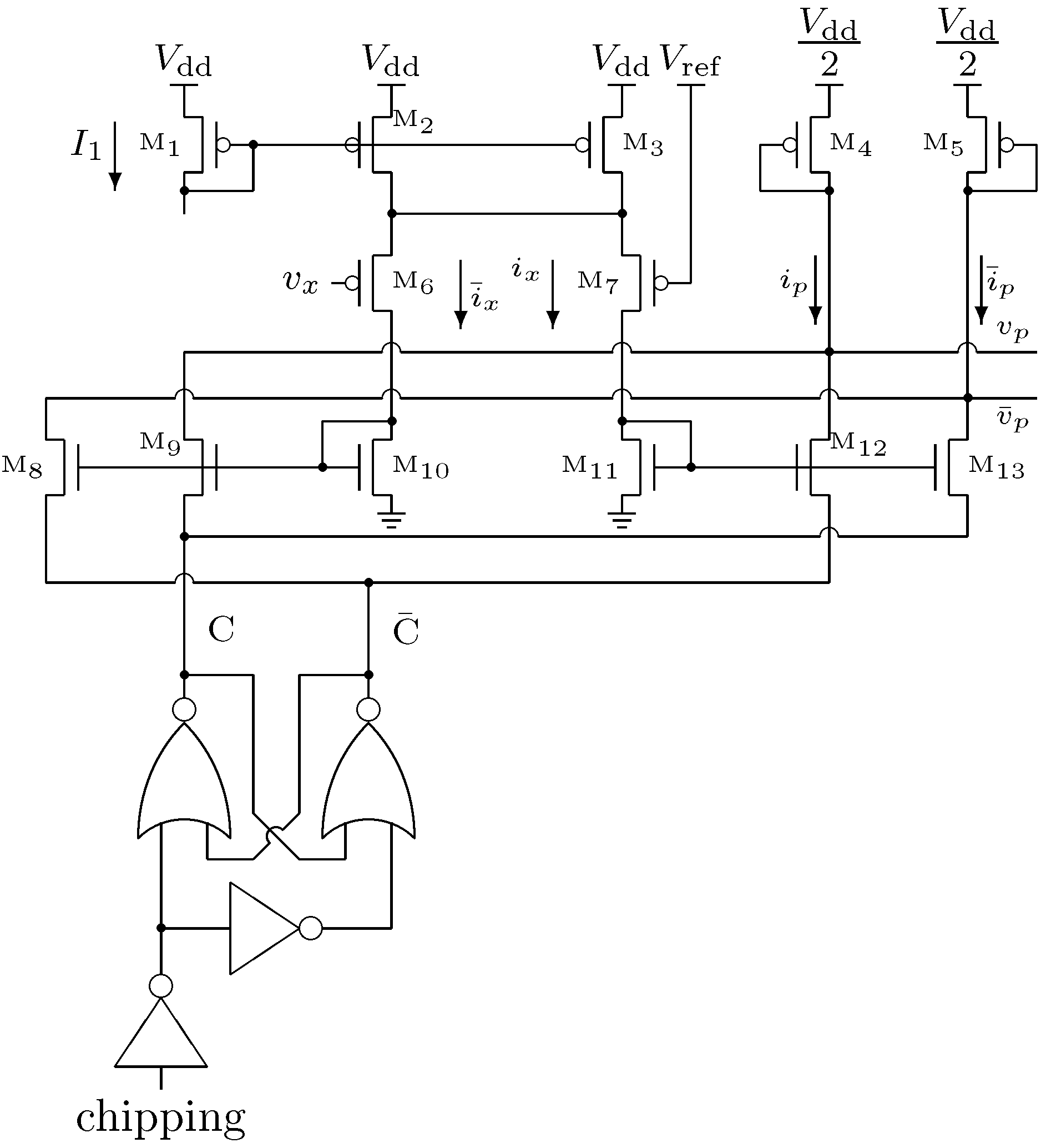
3.2. Modulator Design
Since the input signal is analog, but the chipping sequence is binary, the modulator does not need to be implemented with a full analog multiplier (e.g., Gilbert multiplier). Rather, it is sufficient to invert and select or according to whether is 1 or 0 (0 being the binary representation for a chipping sequence value of −1).
Figure 6.
Modulator circuit schematic.
Figure 6.
Modulator circuit schematic.
The schematic of the modulator is shown in
Figure 6. The input signal
is first converted from a single-ended voltage
to a differential current
by the PMOS source-coupled pair (
–
). Because the process does not provide high value resistances having low parasitic capacitance, source resistors were not used in this version to extend the linear range.
and
are each fed to NMOS mirrors with switched outputs (
–
). The switched currents are then combined into
and
such that
when the chipping sequence is 1, and
when the chipping sequence is 0. The currents
and
are then each fed to the input of a diode-connected PMOS transistor (
–
), nodes
and
respectively, for distribution to the two integrators.
The digital control logic that manages the chipping sequence employs a set-reset latch configured so that the internal chipping signal and its complement are never overlapping in the high state. This ensures that the current in the diode-connected PMOS transistors (–) never go to zero.
Two tail transistors were used for the PMOS source-coupled pair (–) so that the average current density in each transistor in the modulator is the same. This simplifies circuit analysis by giving each transistor consistent current dependent characteristics, such as frequency response.
For high speed inputs, the bias current can be adjusted to ensure that the modulator is operating fast enough to keep up with the input signal. For lower speed inputs, it can be reduced to limit the power dissipation.
Figure 7.
Integrator circuit schematic.
Figure 7.
Integrator circuit schematic.
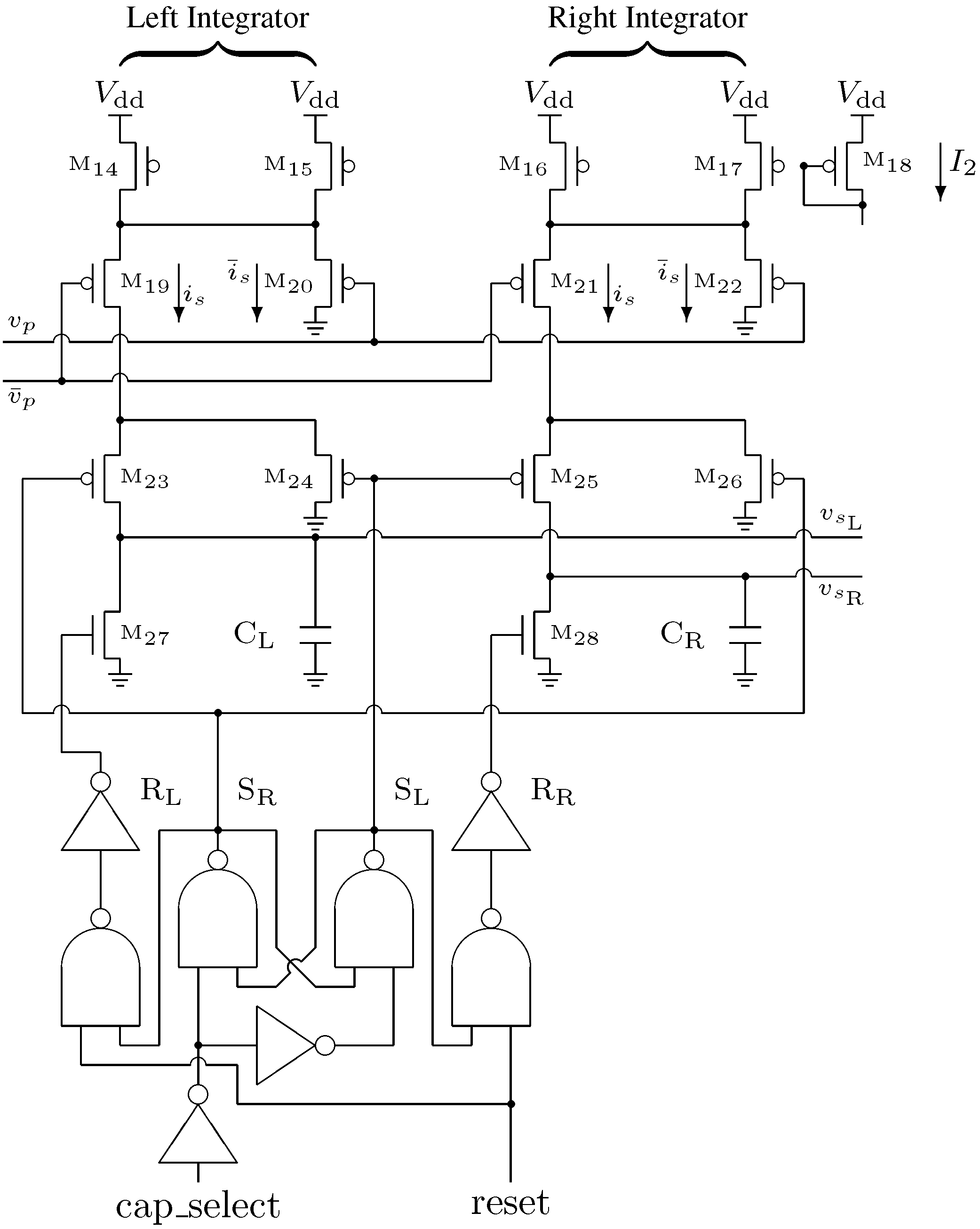
3.3. Integrator Design
The next stage in the analog front-end is the dual integrators, whose circuits are shown in
Figure 7. Because we are operating two integrators in tandem, the integrator circuit is used twice and referred to as the left and right integrators. The modulator output is first scaled by applying
and
to a PMOS source-coupled pair (
–
, or
–
). The resulting current
is fed through a switch to the appropriate integration capacitor (
or
, respectively).
This results in two output signals, and , one from each integration capacitor. The signals controlling the switches are arranged to achieve a ping-pong integration scheme such that only one of the two integrators is integrating at any given moment. The other integrator is in the hold mode and can be reset by asserting the chip’s reset input without affecting the operation of the first integrator.
Due to the inverting nature of the PMOS control switches (–), the integrator digital control logic employs a set-reset latch configured so that the internal select signals and are never overlapping in the low state. This ensures that charge is being deposited on at least one capacitor at all times so that there are no interruptions in the sampling process.
Similar to the modulator circuit, two tail transistors were used for the integrator circuits so that the average current density in each transistor in the integrator is the same. The bias current is used to control the integration range of the front-end. For long integration times or large amplitude input signals, can be reduced to prevent overflowing the charge capacity of the integrators. For short integration times or small amplitude input signals, can be increased to maximize the integrators’ output amplitude. The combined die area consumed by the mixer and integrator for each channel is 14,000
3.4. Two-Input Follower and Output Buffer Design
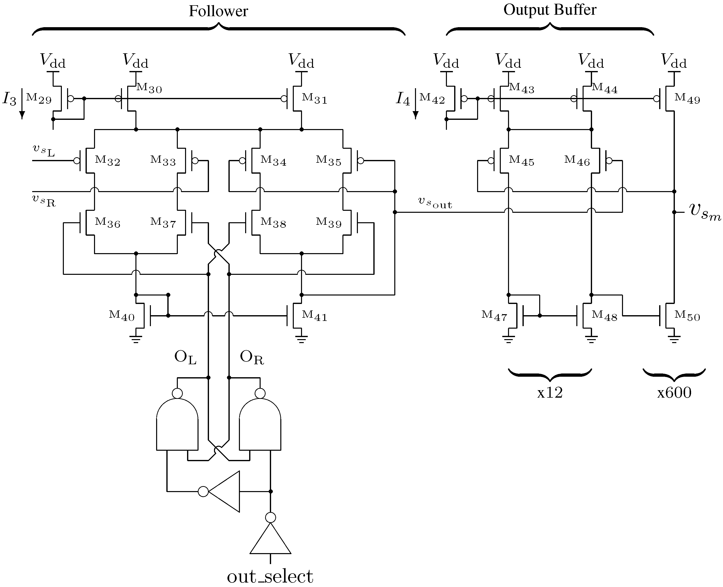
The next stage in the signal chain is the two-input follower shown in
Figure 8. This circuit is derived from the five transistor operational transconductance amplifier (OTA). When the output select input is high,
is copied to the output
otherwise
is copied out.
Figure 8.
Two-input follower and output buffer circuit schematics.
Figure 8.
Two-input follower and output buffer circuit schematics.
The digital control logic for the follower is also configured so that the internal select signals and are never overlapping in the low state. These signals interface with a set of NMOS switches (–), ensuring that only one capacitor node at a time is selected. The die area consumed by the follower for each channel is 7600
In order to achieve a stable output and drive the integrated signal off-chip to be sampled by discrete ADCs, an operational amplifier (OPAMP) was used to buffer the signal. The second section of
Figure 8 shows the circuit schematic for the OPAMP. The output of the analog channel is
and was designed to drive a load of approximately 50 pF at 50
This load is the combined capacitance of the output pad, the chip package and the input of an ADC (e.g., AD7276). In order to achieve this drive capability, each transistor in the first (input) stage of the OPAMP (
–
) is composed of 12 individual transistors in parallel, and each transistor in the second (output) stage (
–
) is composed of 600 individual transistors in parallel. The resulting capacitive load of the output stage is large enough that the OPAMP does not require any additional compensation. The OPAMP consumed 61,000
of die area for each channel. As the capacitors begin their integration after being reset to ground, the OTA and OPAMP circuits were selected for their ability to accurately drive the channel output as close to ground as possible at the required operating frequency.
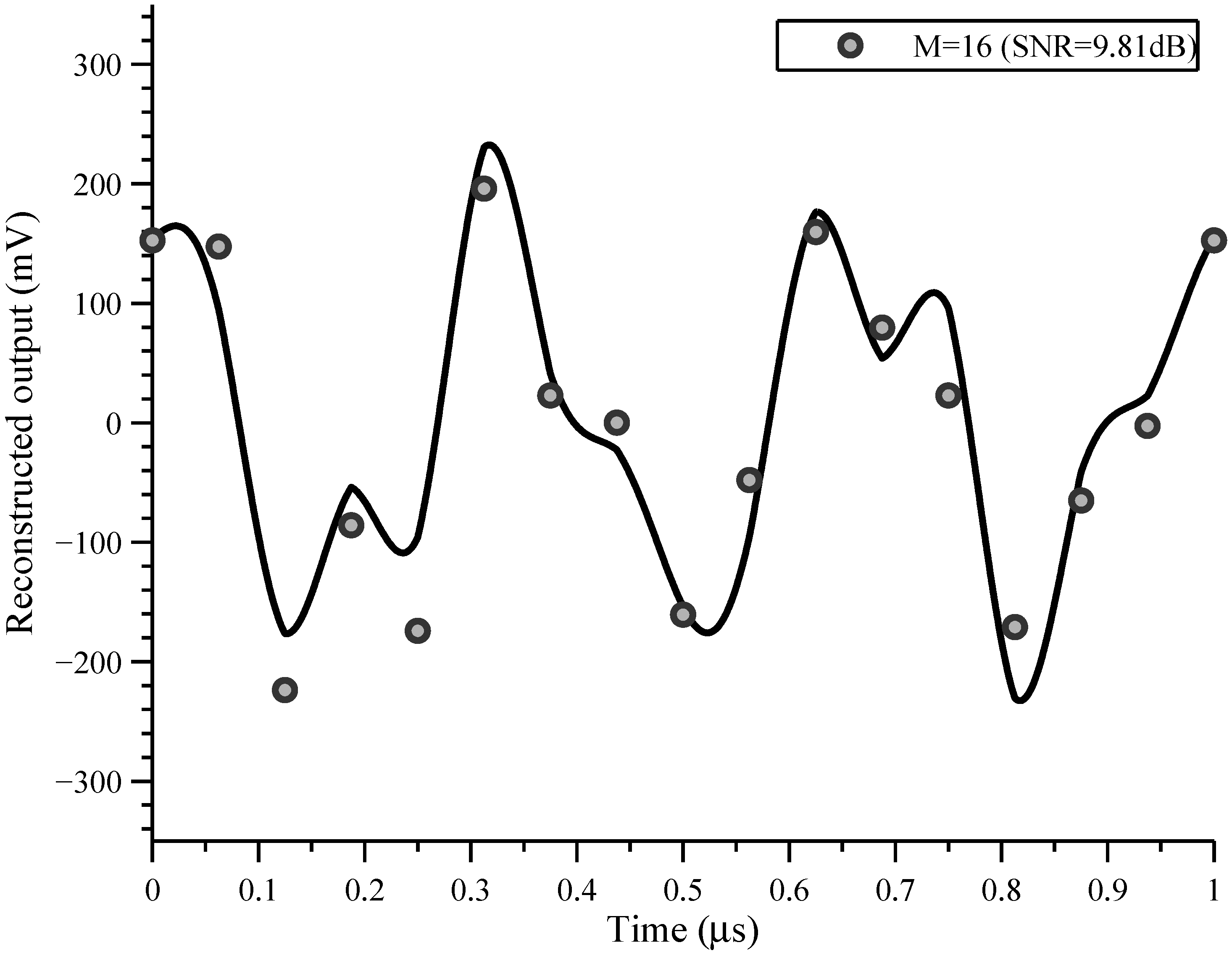
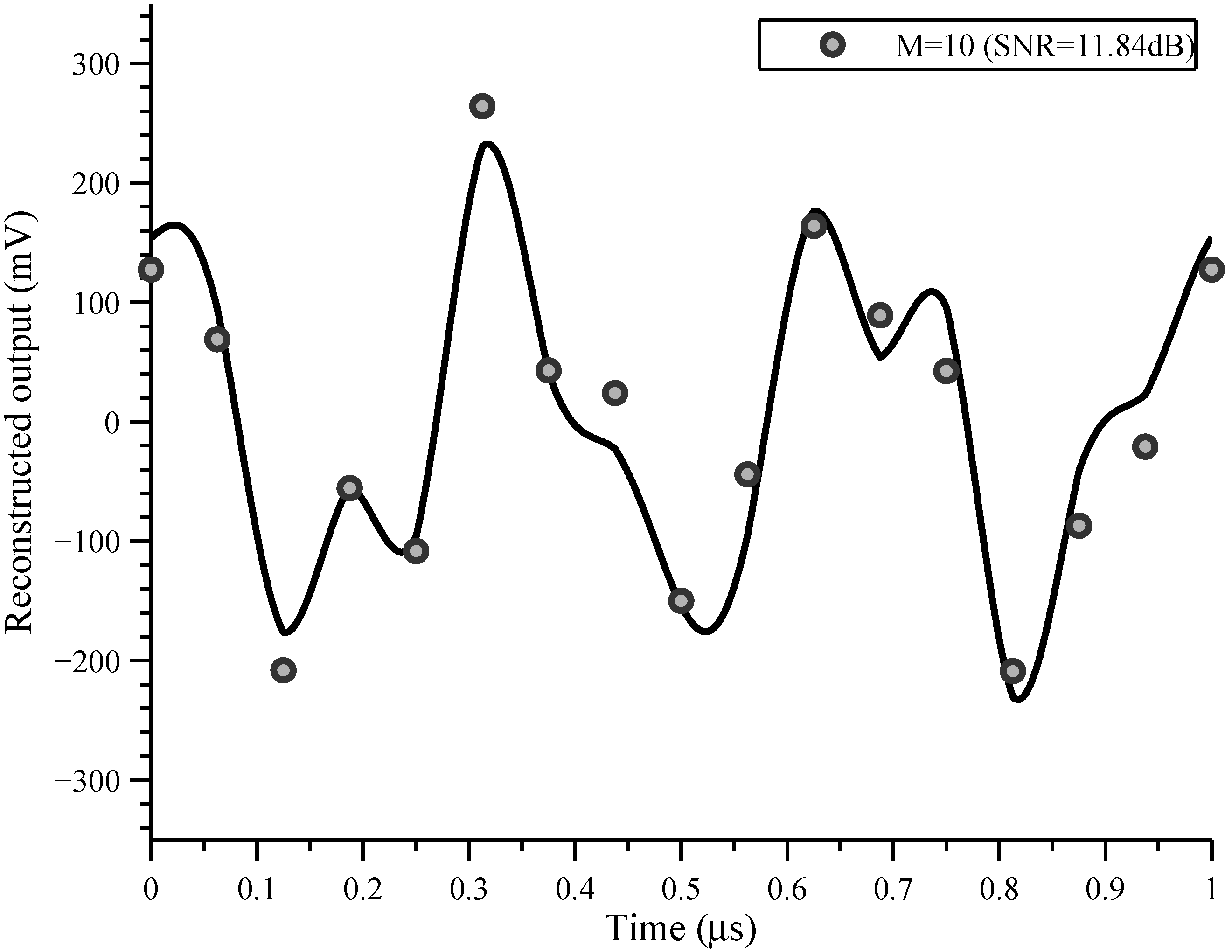
4. Testing
A circuit board with all of the components necessary to support and test the fabricated front-end chip at low speed was developed and is shown in
Figure 9. This test board supports a maximum of two front-end chips for a total of sixteen analog channels.
Figure 9.
Picture of the sampling system prototype.
Figure 9.
Picture of the sampling system prototype.
The board also contains 16 individual ADCs (located under the front-end chips), a single DAC, and an FPGA. Each ADC is a 12-bit 3 Msps converter (AD7276) and is dedicated to digitizing the output of a single analog channel. The DAC is a 14-bit 200 Msps (AD9744 with AD8041 OPAMP) converter that supplies a programmable analog input signal to the front-end chips. The FPGA (XC3S50AN) coordinates the operation of the front-end chips and the data converters. It is responsible for supplying chipping sequences to the front-end chips as well as the input signal in digital form to the DAC. It is also responsible for collecting the ADC samples and relaying them to the host computer via a USB interface.
4.1. Channel Calibration
Before applying actual analog input signals, we first calibrated both integrators (left and right) in each of the sixteen channels. These calibration steps were all performed using constant analog inputs and chipping sequences.
4.1.1. Bias Current Adjustment
The front-end chip uses four bias currents, through to tune the operation of the mixer, integrators, follower and output buffer respectively. and were left at their nominal value of 10 while was tuned to the integration period of 1
To tune analog inputs and chipping sequences must be applied in such a way as to obtain maximum integrator output. This was accomplished using a constant maximal DAC output (DAC set to ) with a constant chipping sequence of as well as a constant minimal DAC output (DAC set to ) with a constant chipping sequence of The bias current was then progressively reduced until the integrators were no longer saturating. The final value of was 0.1
Figure 10.
Channel transfer characteristic.
Figure 10.
Channel transfer characteristic.
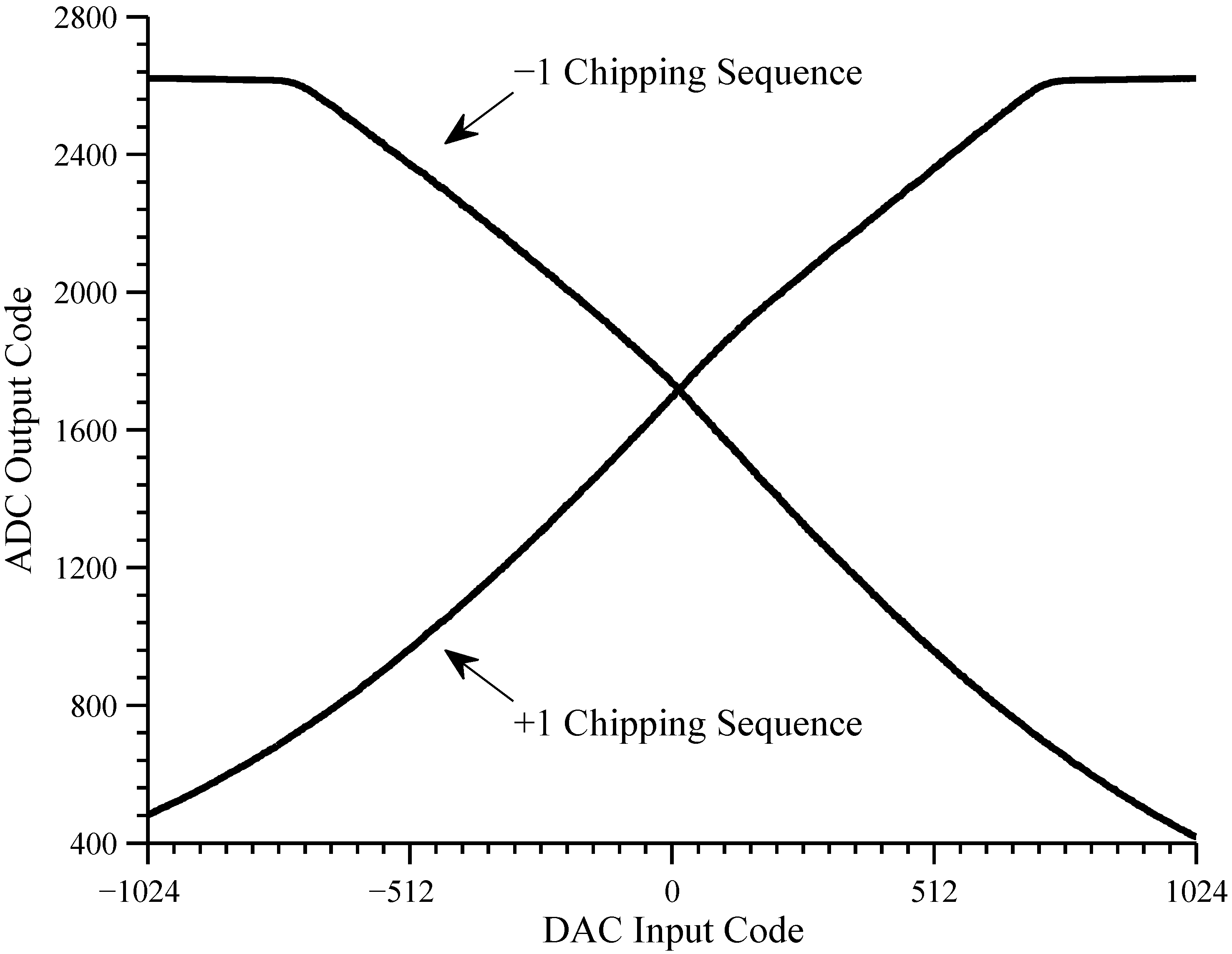
4.1.2. Input Dynamic Range
The front-end chip uses a source-coupled pair to convert the analog input to a current. Since the circuit does not make use of source resistors, the linear region is fairly narrow. The linear region was characterized by sequentially applying constant analog input signals with constant chipping sequences (both and ) for all possible DAC codes ( to ).
The result, reported in
Figure 10, shows that the input saturates at the edges of the range
to
. Therefore we chose the input range
to
, which represents an input dynamic range of approximately ± 30 mV, and avoids the saturation region.
4.1.3. Mixer Symmetry
Ideally, the operation of the front-end should be symmetric, in that if an analog input of v is applied with a chipping sequence, the resulting integrator output should be the same as for an analog input of and a chipping sequence of However, we noted during the input dynamic range test that the operation of the front-end was not symmetric due to transistor mismatch in the mixer. Two causes for the asymmetry were identified.
The first cause is the mismatch between the two transistors forming the source-coupled pair. This introduces an input offset , which can be compensated by adjusting the for each channel. Since this was not an option for the current front-end implementation, we instead corrected for the input offset by adding a constant to the DAC values. This prevented us from operating multiple channels in parallel, and was not by itself sufficient to eliminate all the asymmetry in many channels.
The second cause is the mismatch between the transistors composing the current mirrors. These cause the current gain for a chipping sequence to be different from the current gain for a chipping sequence. Unfortunately, these mismatches cannot be trivially corrected.
The input offset and current mirror gains were estimated for each integrator by applying a constant maximal or minimal analog input and constant chipping sequence of
or
The four corresponding integrator outputs are given by
where
is the output offset. From these relationships, we can extract the offsets and current mirror gains using
In practice however, due to the non-linearity of the source-coupled pair, we first obtained the input offset through an iterative process, in which we computed an input offset from the above equation, and then reapplied the test patterns with the new input offset. This process converged after three to four iterations.
The values shown in
Table 1 are for channel 4L (the left capacitor of the fourth channel) after convergence of the input offset. For this integrator,
,
and
Several other integrators exhibited near perfect symmetry, but many of the remaining integrators exhibited pronounced differences in the current mirror gains.
Table 1.
Symmetry Characterization Table.
Table 1.
Symmetry Characterization Table.
| DAC input | Chipping | Output | Channel 4L |
|---|
| | | 995 |
| | | 998 |
| | | 2405 |
| | | 2411 |
The transfer characteristics for channel 4L (after input offset correction) is shown in
Figure 10. The curve with the positive slope was measured with a constant chipping sequence of
while the curve with the negative slope was measured with a chipping sequence of
Close observation shows that the transfer characteristics are slightly non-linear so that the two curves do not cross at a DAC input of zero.
4.2. Chipping Sequence Sensitivity
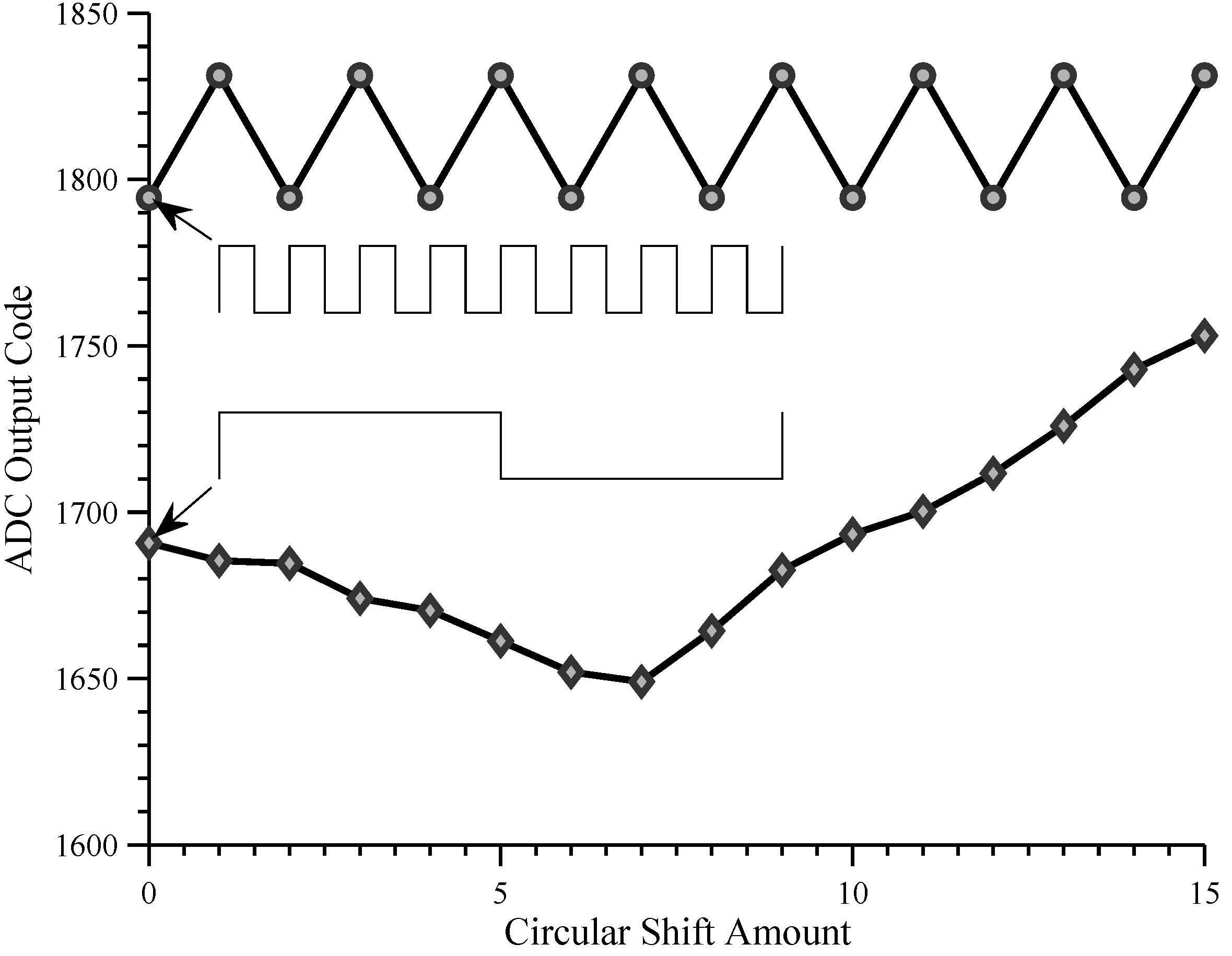
With a constant analog input signal, the integrator output should be insensitive to the order of the chipping sequence bits. For instance, any chipping sequence with zero mean should produce the same integrator output. However, when we switched from using the two possible constant chipping sequences to other chipping sequences, we found that the front-end did not behave as expected.
Figure 11.
Channel 4L output for two circularly shifted chipping sequences.
Figure 11.
Channel 4L output for two circularly shifted chipping sequences.
Figure 11 shows the output of channel 4L for two chipping sequences and a zero constant analog input signal (with input offset correction applied). The first chipping sequence is a square wave with period equal to the integration period (
= 1
), and the second is a square wave with a period of one eighth of the integration period (
). Each chipping sequence was circularly shifted by one sixteenth of the integration period (
or one bit period of the fast square wave).
4.2.1. Circular Shift Sensitivity
For both chipping sequences, the integrator output is sensitive to the circular shift, even though the circular shift does not affect the proportion of to bits. This is probably caused by leakage from the integration capacitor.
4.2.2. Frequency Sensitivity
Although both chipping sequences have zero mean, the integrator output is always lower for the chipping sequence with fewer transitions. This is probably due to charge injection when the chipping input toggles.
4.2.3. Output Offset Correction
The chipping sequence dependent behavior of the front-end chip is particularly problematic with respect to the output offset Normally, can be measured directly by applying a zero constant analog input, and recording the integrator output for each chipping sequence of interest. The recorded output offset can then be subtracted from data subsequently collected with the analog input signals of interest.
Alternatively, the chipping sequence and its complement can be applied with the analog input signal of interest, and the two integrator outputs subtracted. Since the offset being corrected is a property of a given channel, the chipping sequence and the its complement sequence must be applied sequentially to the same channel (this is the
case described at the end of
Section 2.3). Although this requires that the input signal be applied twice, in practice, this gave better results than using the recorded output offsets.
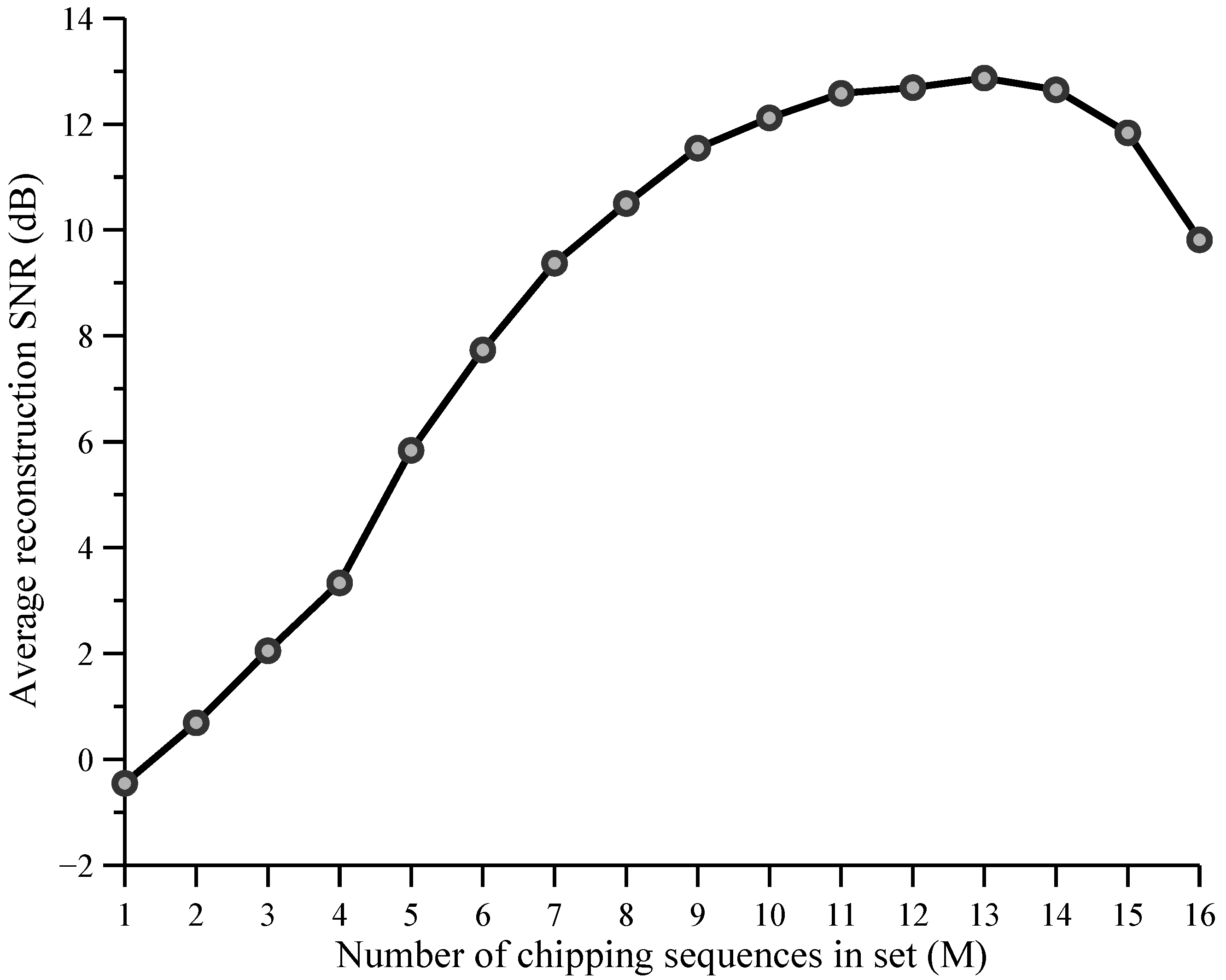
6. Discussion
Today, the vast majority of information processing takes place in the digital domain where computation on large scales has become increasingly cheap and convenient. Unfortunately, there are still many applications that struggle to take advantage of digital computation because the signals involved exceed the capabilities of current physical hardware approaches.
Our performance analysis of the analog front-end provides valuable insights for improvements to be made in the next generation of hardware. Integrating additional discrete components like the channel ADCs into the chip will solve a number of practical issues. Analog signals typically require far more power to drive off chip than digital signals. Replacing the large analog drivers in the existing chip with dedicated ADCs will greatly reduce the complexity of the overall system and provide a more controlled connection between a channel’s integrating node and the ADC. This in turn will allow for smoother operation of the ping-pong sampling scheme.
Technology related practical issues that affect the performance of analog to information converters were discussed in previous papers on the implementation of integrated systems [
26]. Channel matching is clearly a major obstacle for the highly parallel architecture. Furthermore, our current system model assumes that the channel components are linear, limiting its ability to account for the nonlinear behavior exhibited by many of the fabricated components. Nonetheless, our work in this paper is the first experimental realization of an integrated sampler for an analog to information converter where fabrication and implementation related issues are evident in the experimental data. Further work and development of implementation models [
27] for the non-idealities in the system needs to be done before these fabricated systems can achieve their theoretical limits. In future designs, it may be necessary to provide expanded calibration capabilities in addition to redesigning the integrators to provide a more uniform result. It may also be necessary to augment the model to account for some of these nonlinear effects in order to fully explain the reconstruction errors.
Although the prototype system is limited in speed by the fabrication process used and its reliance on external ADCs and digital processing components, it provides an important first step towards a fully integrated system. All the hardware components were designed to allow for the possibility of building data converters in commercial processes with higher effective bandwidths.
Note that the relative simplicity of the circuit elements in the mixer and integrator was intentional and is an important practical consideration for this architecture. Indeed, in order for the architecture to retain its broad applicability, it must necessarily operate near the maximum speed of the fabrication process, independent of which fabrication process is used. This implies that complex circuit elements, such as OPAMPs, cannot be used in the mixer and integrator, because they would limit the speed to such an extent that Nyquist ADCs could be used instead to directly digitize the input signal.
Our D.C. coupled system is complementary to the radio frequency architectures recently reported in [
17,
18]. We expect that further optimization of the circuit components combined with fabrication in a state-of-the-art process will allow our system to span both ranges of operating frequencies. In the future we envision such systems as solid platforms on which to develop a new generation of efficient data converters that improve upon the bandwidth and resolution constraints of conventional ADCs.


