
Organic Photodetectors in Analytical Applications

Abstract
:1. Introduction
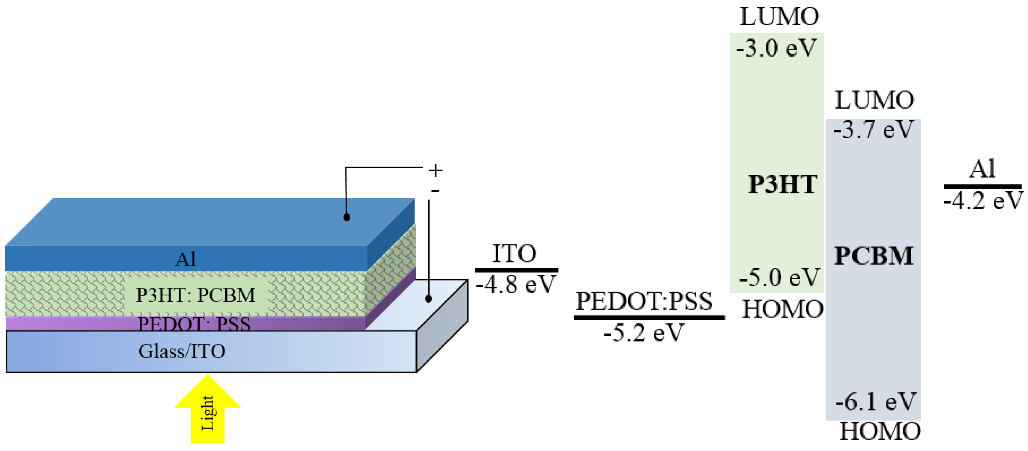
2. Organic Photodetectors: Working Principle

3. OPDs in Analytical Sensing
3.1. Chemiluminescent Assays

3.2. PL-Based Chemical/Biological Sensors


3.3. Light Scattering and Absorption


3.4. On-Chip Spectrometer

4. Examples of Potential Challenges in Sensing with OPDs
4.1. Signal to Noise Ratio

4.2. Stability
4.3. Time Resolved Sensing with OPDs
5. Hybrid Photodetectors


| PD Details | Dark Current (nA/cm2) (Bias, V) | EQE (%) | Responsivity (A/W) | Wavelength Range (nm) | Response Time | Lifetime | Noise | References |
|---|---|---|---|---|---|---|---|---|
| ITO/CuPc:C60/BCP/Al; BHJ | ~6.25 (~0) | 30 | 600–700 | [42] | ||||
| ITO/CuPc/C60/BCP/Ag | ~0 (+0–0.2) | 15–17 | 0.07 @ 493 nm, 0.11 @ 592 nm | - | - | - | [80] | |
| ITO/CuPc/C60/BCP/Ag | 23 | 400–500 | [83] | |||||
| ITO/PEDOT:PSS/CuPc/C60/LiF/Al | 0.83 (~0) | - | 0.008 A/W @ 570 nm | 500–700 | - | 2 weeks | - | [64,65] |
| ITO/CuPc/C60/CuPc/C60/LiF/Al | - | - | 0.023 @ 560 nm | 500–700 | - | - | - | [66] |
| ITO/CuPc/CuPc:C60/C60/BCP/Al Mixed heterojunction | IPCE 19 @ 585 nm | 400–750 | [81] | |||||
| ITO/LiF/CuPc/C70/BPhen/Al | - | 35 @ 640 nm | - | 400–700 | - | - | - | [75] |
| ITO/TPTPA:C70/BCP/Ag | IPCE 44 @ 586 nm | 400–600 | [82] | |||||
| Au (or Au/MoO3)/CuPc/PTCBI/Alq3 (BPhen)/Ag | ~1 nA | 10 @ 600 nm | - | 500–700 | 1.3–1.6 μs (with BPhen) | - | - | [68,69,70,71,72,73,84] |
| ITO/PEDOT:PSS/P3HT:PCBM/Al (or LiF/Al, Ca/Al or Ba/Al as cathode) | 0.1–1 (~0–0.1) | 50–70 | 0.25 | 350–600 | 0.51 μs rise-time; 0.66 μs fall-time (Al cathode) | over 3 years shelf life | ~1 pA @ 1 Hz band-width | [44,45,46,74,77,79,88] |
| ITO/PEDOT:PSS/rr-P3HT:PC61BM/Ca/Ag | ~65 (−5) | 76 (−5 V) | 0.36 | 400–650 | - | over 1 year | 8.2 × 10⁻¹⁴ A/Hz1/2 | [85,86] |
| ITO/PEDOT:PSS/PCDTBT:PC70BM/LiF/Al | 2.8 × 10⁻³ (~0) | 60–70 | 0.22 @ 405 nm | 400–600 | - | 25% photo-current decrease in 15 days | D* ~ 9.2 × 10¹¹ jones | [47,49,50,51,52,53,54] |
| ITO/PTB3:PC61BM/LiF/Al | <1 | 45 @ 685 nm | 0.26 @ 685 nm | 400–750 | 1 μs | - | - | [78] |
| ITO/PEDOT:PSS/PTB7:PCBM/Ca/Al | ~1–2 (~0) | 88 @ 640 nm | - | 400–700 | - | - | - | [77] |
| Conductive PEDOT:PSS/PEDOT:PSS/ PTB7:PC71BM/Al | 1 (−2) | 38 @ 532 nm; 47 @ 626 nm | - | 400–750 | 24% photo-current decrease over 7 days (OLED/OPD lifetime) | [87] | ||
| thin film c-Si | 0.63 (~0) | - | 0.19–0.34 | 470–600 | - | - | - | [114] |
| a-Si:H | 0.01–0.1 (−3) | 50 | - | 500–550 | - | - | - | [115,116] |
| (poly-Si) with interdigitated p-i-n structure | <5 nA | 50 | 0.33 | 850 | - | - | - | [117] |
| PbS colloidal quantum dot | 0.1 | 50 @ 550 nm | 500–1400 | ~300 ns | >2 months | D* ~ 1 × 10¹² jones | [118] | |
| Squaraine-based nanowire/c-Si p-n heterojunction | ~7 × 10⁻³ nA (−1) | 1.3–9.8 | 254–980 | D* 0.06–0.45 × 10¹¹ jones @ −3 V | [121] |
| Detection Approach | PD Type/Active Layer | Analyte | LOD | References | Comments |
|---|---|---|---|---|---|
| CL | CuPc:C60 BHJ | H2O2 | 1 mM | [42] | High LOD due to larger size of the OPD compared to the detection chamber |
| P3HT:PCBM BHJ | H2O2 | 10 μM; | [44] | Results are comparable to inorganic PD (Newport 818 UV Si PD) and PMT (Hamamatsu R3896 and RAPTOR fiber optic biosensor) | |
| Antioxidants | 1–50 μM; | [45] | |||
| Staphylococcal enterotoxin B | 0.5 ng/mL | [46] | |||
| PCDTBT: PC70BM BHJ; ring shaped OPDs | rhTSH | 30–80 pg/mL | [47,49] | Higher detection sensitivity than with a P3HT based PD, excellent linearity, multiplexed detection | |
| Stress hormone cortisol | <0.28 nM | [50] | |||
| E. coli | 5 × 10⁵ cell/mL | [51] | |||
| C. jejuni | 1 × 10⁵ cell/mL | ||||
| Adenovirus | 1 × 10⁻⁸ mg/mL | ||||
| 17-β estradiol | 2.5 pg/mL | [53] | |||
| Legionella pneumophila | 4 × 10⁴ cell/mL | [54] | |||
| a-Si:H | HRP | 0.2 amol | [119] | ||
| Metal semiconductor (c-Si n+) metal PD | Streptavidin | 4.76 nM | [120] | ||
| PL | CuPc-C60 | Rhodamine 6G | 10 nM (halide excitation), 100 nM (OLED excitation) | [64,65] | |
| Fluorescein | 10 nM (halide), 10 μM (OLED) | ||||
| Resorufin | 5.0 μM | [80] | |||
| IgA | 16 ng/mL | ||||
| malachite green, phosphate | 0.02 ppm | [83] | |||
| Bilayer CuPc/C60 | Rhodamine 6G | 10 nM | [66] | ||
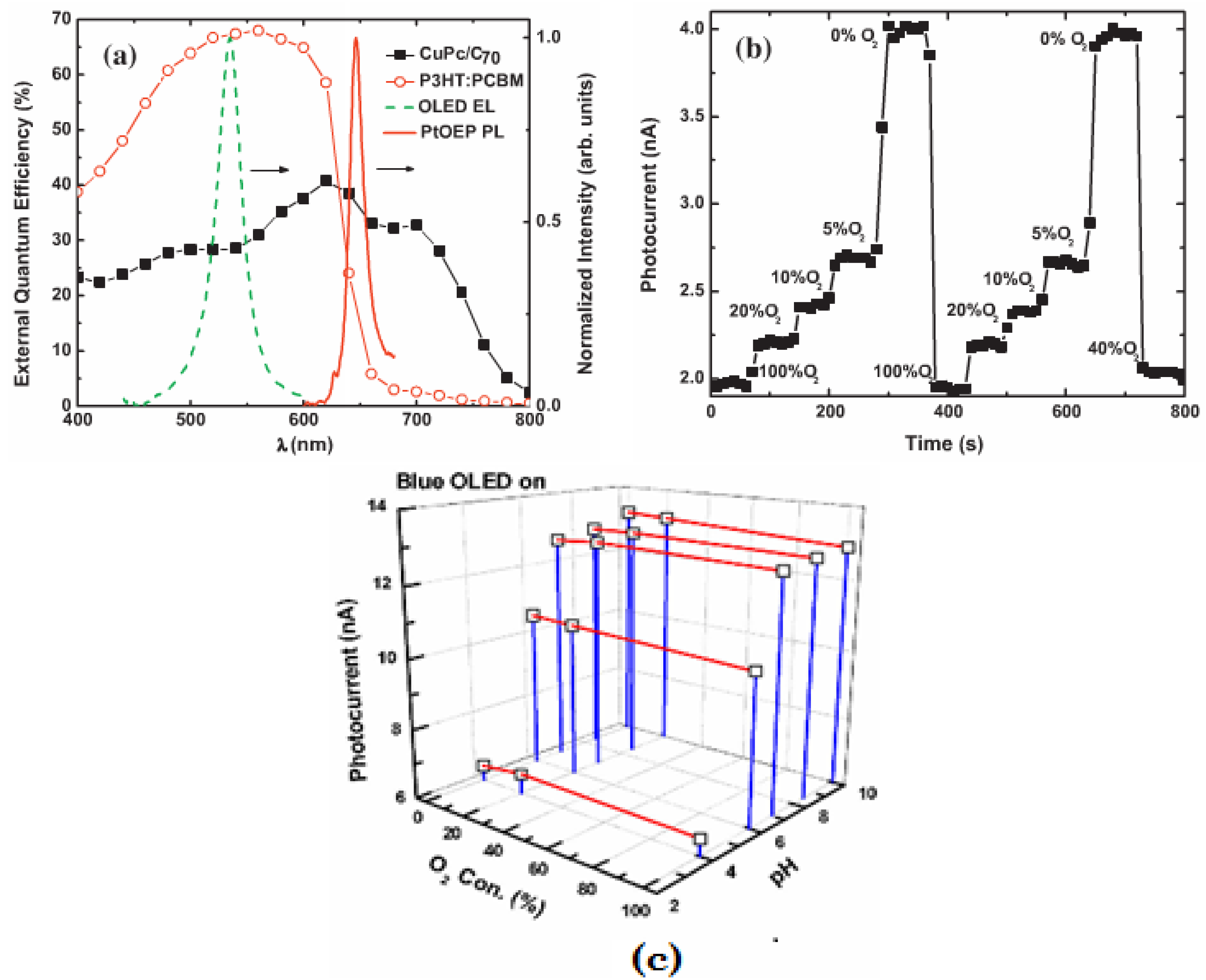
| CuPc/C70 | O2, pH | - | [75] | Time-resolved sensing | |
| CuPc/CuPc:C60/C60 mixed heterojunction | APnEOs | 2–4 ppb | [81] | ||
| CuPc/PTCBI | Various indicators for O2, CO2, pH | - | [68,69,70,71,72,73,84] | ring shaped OPD | |
| TPTPA:C70 | resorufin | 0.6 μM | [82] | - | |
| APnEOs | 1–2 ppb | ||||
| P3HT:PCBM BHJ | O2, β-d-glucose | - | [74] | Time resolved sensing | |
| Diuron | 11nM | [78] | higher sensitivity than commercial biosensors (Handy-PEA fluorometer) | ||
| myoglobin, CK-MB | 1.5 ng/mL | [79] | Higher photoresponse than Si (Osram Opto Semiconductors, SFH2430) | ||
| PTB7:PC61BM BHJ | O2 | - | [77] | - | |
| a-Si:H | Fluorescein | 680 pM; 17 nM (with integrated PD on microchip) | [115] | - | |
| Green fluorescent protein | 18.5 nM | [116] | |||
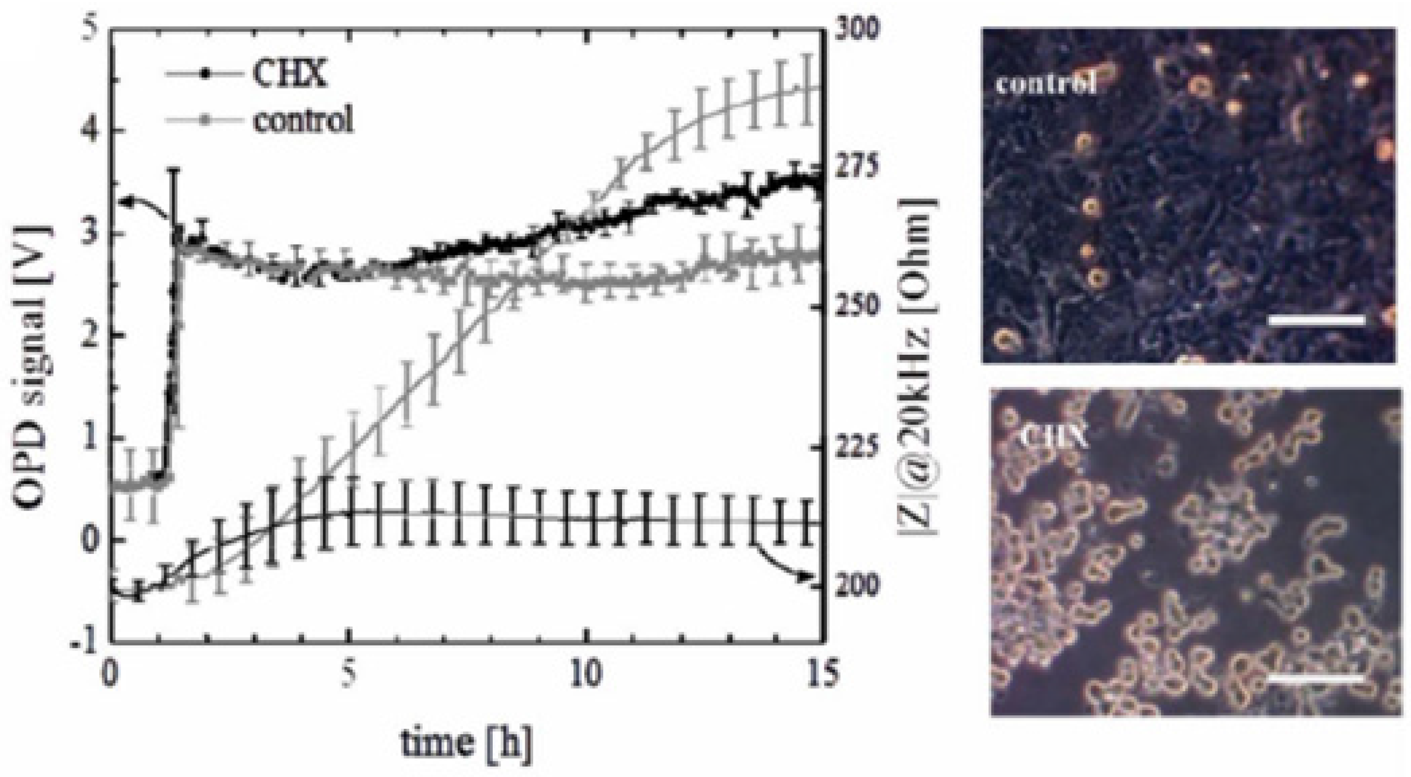
| Light scattering | Regioregular P3HT:PC61BM BHJ | Living HELA cells | <1000 cells/cm2 | [85,86] | Label free monitoring |
| calcein-AM | - | ||||
| PTB3:PC61BM BHJ | Mouse immuno-globulin G | 5 nm spectral resolution | [88] | Grating-based spectrometer | |
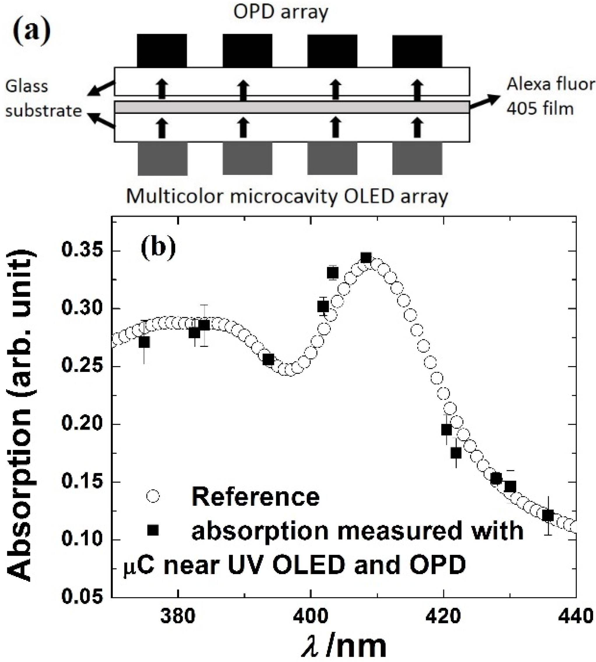
| Absorption | P3HT:PC61BM BHJ | Alexa Fluor 405 | 5–10 nm spectral resolution | [77] | Absorption based spectrometer |
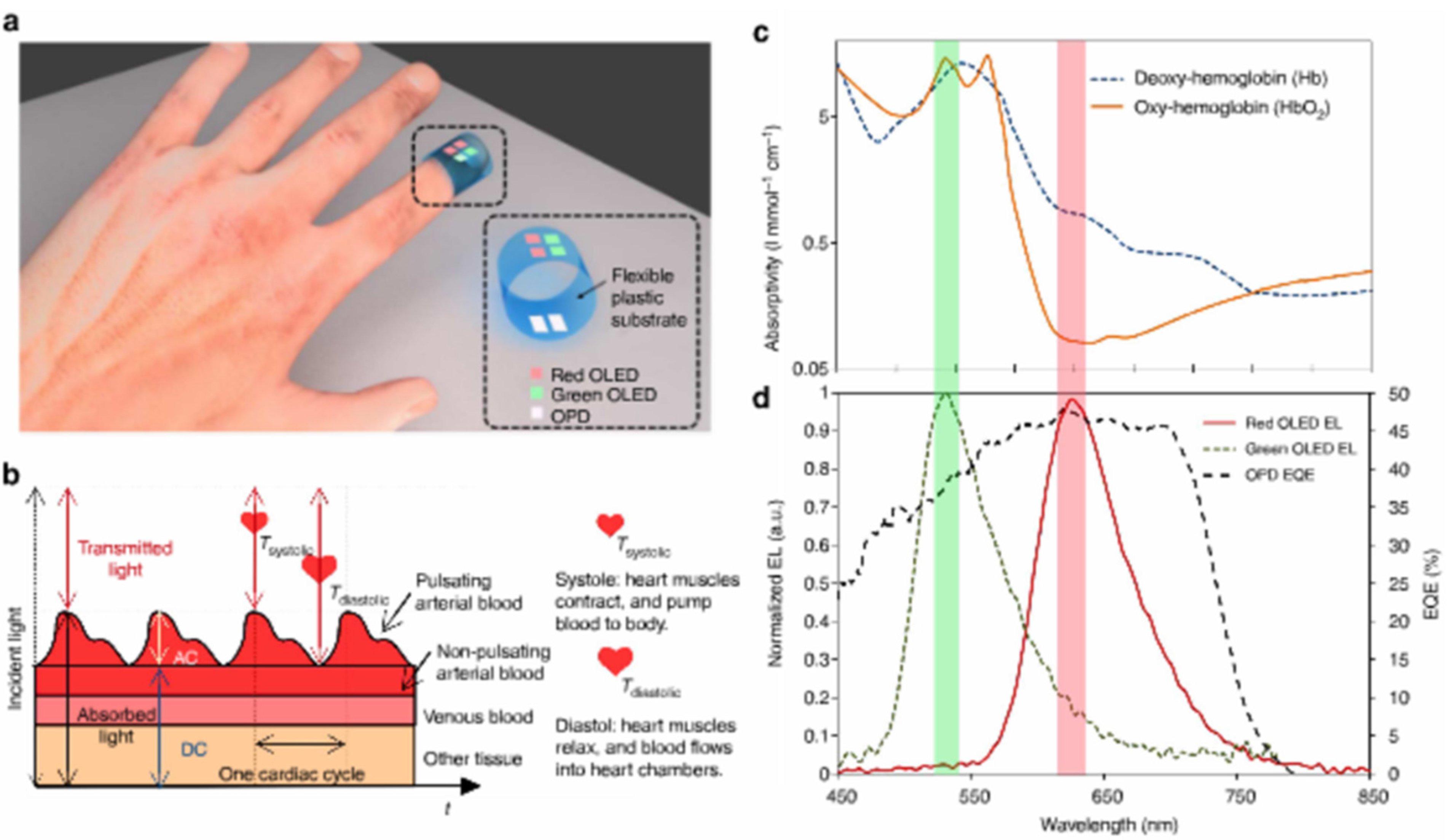
| PTB7:PC71BM BHJ | Oxy hemoglobin | - | [87] | Flexible integrated sensor, pulsed oximetry |
- We note that the dark current at nominally 0 V bias may be due to an actual small voltage and some remnant light.
- The structure of the OPDs is planar heterojunction, unless specified otherwise.
6. Concluding Remarks and Outlook
Acknowledgments
Author Contributions
Conflicts of Interest
References
- Sensors Trends 2014; Großer, V.; Heydenbluth, D.; Moos, R.; Rein, D.; Sauerer, J.; Simmons, C.T.; Sinn, W.; Werthschützky, R.; Wilde, J. (Eds.) AMA Association for Sensor Technology: Berlin, Germany, 2010.
- Shinar, J.; Shinar, R. Organic light-emitting devices (OLEDs) and OLED-based chemical and biological sensors: An overview. J. Phys. D Appl. Phys. 2008. [Google Scholar] [CrossRef]
- Wang, X.D.; Wolfbeis, O.S. Optical methods for sensing and imaging oxygen: Materials, spectroscopies and applications. Chem. Soc. Rev. 2014, 43, 3666–3761. [Google Scholar] [CrossRef] [PubMed]
- Williams, G.; Backhouse, C.; Aziz, H. Integration of Organic Light Emitting Diodes and Organic Photodetectors for Lab-on-a-Chip Bio-Detection Systems. Electronics 2014, 3, 43–75. [Google Scholar] [CrossRef]
- Ren, K.N.; Liang, Q.L.; Yao, B.; Luo, G.O.; Wang, L.D.; Gao, Y.; Wang, Y.M.; Qiu, Y. Whole column fluorescence imaging on a microchip by using a programmed organic light emitting diode array as a spatial-scanning light source and a single photomultiplier tube as detector. Lab Chip 2007, 7, 1574–1580. [Google Scholar] [CrossRef] [PubMed]
- Yao, B.; Yang, H.; Liang, Q.; Luo, G.; Wang, L.; Ren, K.; Gao, Y.; Wang, Y.; Qiu, Y. High-speed, whole-column fluorescence imaging detection for isoelectric focusing on a microchip using an organic light emitting diode as light source. Anal. Chem. 2006, 78, 5845–5850. [Google Scholar] [CrossRef] [PubMed]
- Choudhury, B.; Shinar, R.; Shinar, J. Glucose biosensors based on organic light-emitting devices structurally integrated with a luminescent sensing element. J. Appl. Phys. 2004, 96, 2949–2954. [Google Scholar] [CrossRef]
- Liu, R.; Cai, Y.; Park, J.-M.; Ho, K.-M.; Shinar, J.; Shinar, R. Organic Light-Emitting Diode Sensing Platform: Challenges and Solutions. Adv. Funct. Mater. 2011, 21, 4744–4753. [Google Scholar] [CrossRef]
- Wolfbeis, O.S.; Offenbacher, H.; Kroneis, H.; Marsoner, H. A fast responding fluorescence sensor for oxygen. Microchim. Acta 1984, 82, 153–158. [Google Scholar] [CrossRef]
- You, Y.; Park, S.Y. A Phosphorescent Ir (III) Complex for Selective Fluoride Ion Sensing with a High Signal-to-Noise Ratio. Adv. Mater. 2008, 20, 3820–3826. [Google Scholar] [CrossRef]
- McDonagh, C.; MacCraith, B.D.; McEvoy, A.K. Tailoring of sol-gel films for optical sensing of oxygen in gas and aqueous phase. Anal. Chem. 1998, 70, 45–50. [Google Scholar] [CrossRef] [PubMed]
- Cai, Y.; Shinar, R.; Zhou, Z.; Shinar, J. Multianalyte sensor array based on an organic light emitting diode platform. Sens. Actuator B 2008, 134, 727–735. [Google Scholar] [CrossRef]
- Yu, G.; Pakbaz, K.; Heeger, A.J. Semiconducting polymer diodes: Large size, low cost photodetectors with excellent visible-ultraviolet sensitivity. Appl. Phys. Lett. 1994, 64, 3422–3424. [Google Scholar] [CrossRef]
- Forrest, S. The path to ubiquitous and low-cost organic electronic appliances on plastic. Nature 2004, 428, 911–918. [Google Scholar] [CrossRef] [PubMed]
- Krebs, F.C. Fabrication and processing of polymer solar cells: A review of printing and coating techniques. Sol. Energy Mater. Sol. Cells 2009, 93, 394–412. [Google Scholar] [CrossRef]
- Peumans, P.; Uchida, S.; Forrest, S.R. Efficient bulk heterojunction photovoltaic cells using small-molecular-weight organic thin films. Nature 2003, 425, 158–162. [Google Scholar] [CrossRef] [PubMed]
- Baierl, D.; Fabel, B.; Lugli, P.; Scarpa, G. Efficient indium-tin-oxide (ITO) free top-absorbing organic photodetector with highly transparent polymer top electrode. Org. Electron. 2011, 12, 1669–1673. [Google Scholar] [CrossRef]
- Abdellah, A.; Fabel, B.; Lugli, P.; Scarpa, G. Spray deposition of organic semiconducting thin-films: Towards the fabrication of arbitrary shaped organic electronic devices. Org. Electron. 2010, 11, 1031–1038. [Google Scholar] [CrossRef]
- Aernouts, T.; Aleksandrov, T.; Girotto, C.; Genoe, J.; Poortmans, J. Polymer based organic solar cells using ink-jet printed active layers. Appl. Phys. Lett. 2008. [Google Scholar] [CrossRef]
- Ng, T.N.; Wong, W.S.; Chabinyc, M.L.; Sambandan, S.; Street, R.A. Flexible image sensor array with bulk heterojunction organic photodiode. Appl. Phys. Lett. 2008. [Google Scholar] [CrossRef]
- An, K.H.; O’Connor, B.; Pipe, K.; Shtein, M. Organic photodetector with spectral response tunable across the visible spectrum by means of internal optical microcavity. Org. Electron. 2009, 10, 1152–1157. [Google Scholar] [CrossRef]
- Tvingstedt, K.; Zilio, D.S.; Inganäs, O.; Tormen, M. Trapping light with micro lenses in thin film organic photovoltaic cells. Opt. Express 2008, 16, 21609–21615. [Google Scholar] [CrossRef]
- Zhu, K.; Neale, N.R.; Miedaner, A.; Frank, A.J. Enhanced charge-collection efficiencies and light scattering in dye-sensitized solar cells using oriented TiO2 nanotubes arrays. Nano Lett. 2007, 7, 69–74. [Google Scholar] [CrossRef] [PubMed]
- Peumans, P.; Bulović, V.; Forrest, S.R. Efficient photon harvesting at high optical intensities in ultrathin organic double-heterostructure photovoltaic diodes. Appl. Phys. Lett. 2000, 76, 2650–2652. [Google Scholar] [CrossRef]
- Duche, D.; Torchio, P.; Escoubas, L.; Monestier, F.; Simon, J.-J.; Flory, F.; Mathian, G. Improving light absorption in organic solar cells by plasmonic contribution. Sol. Energy Mater. Sol. Cells 2009, 93, 1377–1382. [Google Scholar] [CrossRef]
- Park, S.H.; Roy, A.; Beaupré, S.; Cho, S.; Coates, N.; Moon, J.S.; Moses, D.; Leclerc, M.; Lee, K.; Heeger, A.J. Bulk heterojunction solar cells with internal quantum efficiency approaching 100%. Nat. Photonics 2009, 3, 297–303. [Google Scholar] [CrossRef]
- Günes, S.; Neugebauer, H.; Sariciftci, N.S. Conjugated Polymer-Based Organic Solar Cells. Chem. Rev. 2007, 107, 1324–1338. [Google Scholar] [CrossRef] [PubMed]
- Guo, F.; Xiao, Z.; Huang, J. Fullerene Photodetectors with a Linear Dynamic Range of 90 dB Enabled by a Cross-Linkable Buffer Layer. Adv. Opt. Mater. 2013, 1, 289–294. [Google Scholar] [CrossRef]
- Blum, L.J.; Marquette, C.A. Chemiluminescence-based sensors. In Optical Chemical Sensors; Baldini, F., Chester, A.N., Homola, J., Martellucci, S., Eds.; Springer Science & Business Media: Dordrecht, The Netherlands, 2006; pp. 157–178. [Google Scholar]
- Juris, A.; Balzani, V.; Barigelletti, F.; Campagna, S. Ru (II) polypyridine complexes: Photophysics, photochemistry, eletrochemistry, and chemiluminescence. Coord. Chem. Rev. 1988, 84, 85–277. [Google Scholar] [CrossRef]
- Flecha, B.G.; Llesuy, S.; Boveris, A. Hydroperoxide-initiated chemiluminescence: An assay for oxidative stress in biopsies of heart, liver, and muscle. Free Radic. Biol. Med. 1991, 10, 93–100. [Google Scholar] [CrossRef]
- Sigvardson, K.W.; Kennish, J.M.; Birks, J.W. Peroxyoxalate chemiluminescence detection of polycyclic aromatic amines in liquid chromatography. Anal. Chem. 1984, 56, 1096–1102. [Google Scholar] [CrossRef]
- Allen, R.C.; Loose, L.D. Phagocytic activation of a luminol-dependent chemiluminescence in rabbit alveolar and peritoneal macrophages. Biochem. Biophys. Res. Commun. 1976, 69, 245–252. [Google Scholar] [CrossRef]
- Boveris, A.; Cadenas, E.; Chance, B. Ultraweak chemiluminescence: A sensitive assay for oxidative radical reactions. Fed. Proc. 1981, 40, 195–198. [Google Scholar] [PubMed]
- Braman, R.S.; Hendrix, S.A. Nanogram nitrite and nitrate determination in environmental and biological materials by vanadium (III) reduction with chemiluminescence detection. Anal. Chem. 1989, 61, 2715–2718. [Google Scholar] [CrossRef] [PubMed]
- Hanaoka, N.; Tanaka, H.; Nakamoto, A.; Takada, M. Kinetic study of background emission from peroxyoxalate chemiluminescence reaction and application to the improvement of detection limits in liquid chromatography. Anal. Chem. 1991, 63, 2680–2685. [Google Scholar] [CrossRef]
- Andrew, K.N.; Sanders, M.G.; Forbes, S.; Worsfold, P.J. Flow methods for the determination of polycyclic aromatic hydrocarbons using low power photomultiplier tube and charge coupled device chemiluminescence detection. Anal. Chim. Acta 1997, 346, 113–120. [Google Scholar] [CrossRef]
- Amatatongchai, M.; Hofmann, O.; Nacapricha, D.; Chailapakul, O.; de Mello, A.J. A microfluidic system for evaluation of antioxidant capacity based on a peroxyoxalate chemiluminescence assay. Anal. Bioanal. Chem. 2007, 387, 277–285. [Google Scholar] [CrossRef] [PubMed]
- Gachanja, A.; Worsfold, P. Determination of aliphatic carboxylic acids in non-aqueous matrices by liquid chromatography with peroxyoxalate chemiluminescence detection. Anal. Chim. Acta 1994, 290, 226–232. [Google Scholar] [CrossRef]
- Knight, A.W.; Greenway, G.M.; Chesmore, E.D. Development of a silicon photodiode, electrogenerated chemiluminescence, flow-through detector. Anal. Proc. 1995, 32, 125–127. [Google Scholar] [CrossRef]
- Pereira, A.T.; Novo, P.; Prazeres, D.; Chu, V.; Conde, J.P. Heterogeneous immunoassays in microfluidic format using fluorescence detection with integrated amorphous silicon photodiodes. Biomicrofluidics 2011. [Google Scholar] [CrossRef] [PubMed]
- Hofmann, O.; Miller, P.; Sullivan, P.; Jones, T.S.; de Mello, J.C.; Bradley, D.D.C.; de Mello, A.J. Thin-film organic photodiodes as integrated detectors for microscale chemiluminescence assays. Sens. Actuators B 2005, 106, 878–884. [Google Scholar]
- Jorgensen, A.M.; Mogensen, K.B.; Kutter, J.P.; Geschke, O. A biochemical microdevice with an integrated chemiluminescence detector. Sens. Actuators B 2003, 90, 15–21. [Google Scholar] [CrossRef]
- Wang, X.; Hofmann, O.; Das, R.; Barrett, E.; de Mello, A.J.; de Mello, J.C.; Bradley, D. Integrated thin-film polymer/fullerene photodetectors for on-chip microfluidic chemiluminescence detection. Lab Chip 2007, 7, 58–63. [Google Scholar] [CrossRef] [PubMed]
- Wang, X.; Amatatongchai, M.; Nacapricha, D.; Hofmann, O.; de Mello, J.C.; Bradley, D.D.C.; de Mello, A.J. Thin-film organic photodiodes for integrated on-chip chemiluminescence detection-application to antioxidant capacity screening. Sens. Actuators B 2009, 140, 643–648. [Google Scholar] [CrossRef]
- Wojciechowski, J.; Shriver-Lake, L.; Yamaguchi, M.; Füreder, E.; Pieler, R.; Schamesberger, M.; Winder, C.; Prall, H.; Sonnleitner, M.; Ligler, F. Organic Photodiodes for Biosensor Miniaturization. Anal. Chem. 2009, 81, 3455–3461. [Google Scholar] [CrossRef] [PubMed]
- Pires, N.; Dong, T. Polycarbazole-based organic photodiodes for highly sensitive chemiluminescent immunoassays. In Proceedings of the Annual International Conference of the IEEE Engineering in Medicine and Biology Society, Osaka, Japan, 3–7 July 2013; pp. 1700–1703.
- Lim, K.-G.; Choi, M.-R.; Kim, H.-B.; Park, J.H.; Lee, T.-W. High-efficiency polymer photovoltaic cells using a solution-processable insulating interfacial nanolayer: The role of the insulating nanolayer. J. Mater. Chem. 2012, 22, 25148–25153. [Google Scholar] [CrossRef]
- Pires, N.; Dong, T.; Hanke, U.; Hoivik, N. Integrated optical microfluidic biosensor using a polycarbazole photodetector for point-of-care detection of hormonal compounds. J. Biomed. Opt. 2013. [Google Scholar] [CrossRef] [PubMed]
- Pires, N.M.; Dong, T. Detection of stress hormones by a microfluidic-integrated polycarbazole/fullerene photodetector. In Proceedings of the 2013 35th Annual International Conference of the IEEE Engineering in Medicine and Biology Society (EMBC), Osaka, Japan, 3–7 July 2013; pp. 4470–4473.
- Pires, N.M.M.; Dong, T. Microfluidic Biosensor Array with Integrated Poly (2,7-Carbazole)/Fullerene-Based Photodiodes for Rapid Multiplexed Detection of Pathogens. Sensors 2013, 13, 15898–15911. [Google Scholar] [CrossRef] [PubMed]
- Honrado, C.; Dong, T. Development and optimization of an integrated capillary-based opto-microfluidic device for chemiluminescence quantitative detection. J. Micromech. Microeng. 2014. [Google Scholar] [CrossRef]
- Pires, N.; Dong, T. Ultrasensitive opto-microfluidic immunosensor integrating gold nanoparticle enhanced chemiluminescence and highly stable organic photodetector. J. Biomed. Opt. 2014. [Google Scholar] [CrossRef] [PubMed]
- Pires, N.; Dong, T. An integrated passive-flow microfluidic biosensor with organic photodiodes for ultra-sensitive pathogen detection in water. In Proceedings of the 36th Annual International Conference of the IEEE Engineering in Medicine and Biology Society (EMBC), Chicago, IL, 26–30 August 2014; pp. 4411–4414.
- Hartmann, P.; Leiner, M.J.; Lippitsch, M.E. Luminescence quenching behavior of an oxygen sensor based on a Ru (II) complex dissolved in polystyrene. Anal. Chem. 1995, 67, 88–93. [Google Scholar] [CrossRef]
- Wolfbeis, O.S.; Klimant, I.; Werner, T.; Huber, C.; Kosch, U.; Krause, C.; Neurauter, G.; Dürkop, A. Set of luminescence decay time based chemical sensors for clinical applications. Sens. Actuators B 1998, 51, 17–24. [Google Scholar] [CrossRef]
- O’Riordan, T.C.; Buckley, D.; Ogurtsov, V.; O’Connor, R.; Papkovsky, D.B. A cell viability assay based on monitoring respiration by optical oxygen sensing. Anal. Biochem. 2000, 278, 221–227. [Google Scholar] [CrossRef] [PubMed]
- Sailor, M.J.; Wu, E.C. Photoluminescence-Based Sensing with Porous Silicon Films, Microparticles, and Nanoparticles. Adv. Funct. Mater. 2009, 19, 3195–3208. [Google Scholar] [CrossRef]
- Shinar, R.; Ghosh, D.; Choudhury, B.; Noack, M.; Dalal, V.L.; Shinar, J. Luminescence-based oxygen sensor structurally integrated with an organic light-emitting device excitation source and an amorphous Si-based photodetector. J. Non-Cryst. Solids 2006, 352, 1995–1998. [Google Scholar] [CrossRef]
- Berezin, M.Y.; Achilefu, S. Fluorescence Lifetime Measurements and Biological Imaging. Chem. Rev. 2010, 110, 2641–2684. [Google Scholar] [CrossRef] [PubMed]
- Kautsky, H. Quenching of luminescence by oxygen. Trans. Faraday Soc. 1939, 35, 216–219. [Google Scholar] [CrossRef]
- Choudhury, B.; Shinar, R.; Shinar, J. Luminescent chemical and biological sensors based on the structural integration of an OLED excitation source with a sensing component. Proc. SPIE 2004, 5214, 64–71. [Google Scholar]
- Shinar, R.; Choudhury, B.; Zhou, Z.; Wu, H.-S.; Tabatabai, L.B.; Shinar, J. Structurally integrated organic light-emitting device-based sensors for oxygen, glucose, hydrazine, and anthrax. Proc. SPIE 2004, 5588, 59–69. [Google Scholar]
- Banerjee, A.; Pais, A.; Papautsky, I.; Klotzkin, D. A Polarization Isolation Method for High-Sensitivity, Low-Cost on-Chip Fluorescence Detection for Microfluidic Lab-on-a-Chip. IEEE Sens. J. 2008, 8, 621–627. [Google Scholar] [CrossRef]
- Pais, A.; Banerjee, A.; Klotzkin, D.; Papautsky, I. High-sensitivity, disposable lab-on-a-chip with thin-film organic electronics for fluorescence detection. Lab Chip 2008, 8, 794–800. [Google Scholar] [CrossRef] [PubMed]
- Shuai, Y.; Banerjee, A.; Klotzkin, D.; Papautsky, I. On-chip fluorescence detection with organic thin film devices for disposable lab-on-a-chip sensors. In Proceedings of the 2008 IEEE Sensors, Lecce, Italy, 26–29 October 2008.
- Banerjee, A.; Shuai, Y.; Klotzkin, D.; Papautsky, I. High-Sensitivity Mems Based On-Chip Fluorescence Detection System: Measurement and Analysis of Ultimate Sensitivity Limits. In Proceedings of the 17th Biennial University/Government/Industry Micro/Nano Symposium, Louisville, KY, USA, 13–16 July 2008; pp. 177–182.
- Kraker, E.; Haase, A.; Lamprecht, B.; Jakopic, G.; Konrad, C.; Köstler, S. Integrated organic electronic based optochemical sensors using polarization filters. Appl. Phys. Lett. 2008. [Google Scholar] [CrossRef]
- Mayr, T.; Abel, T.; Kraker, E.; Köstler, S.; Haase, A.; Konrad, C.; Tscherner, M.; Lamprecht, B. An optical sensor array on a flexible substrate with integrated organic opto-electric devices. Procedia Eng. 2010, 5, 1005–1008. [Google Scholar] [CrossRef]
- Abel, T.; Sagmeister, M.; Lamprecht, B.; Kraker, E.; Köstler, S.; Ungerböck, B.; Mayr, T. Filter-free integrated sensor array based on luminescence and absorbance measurements using ring-shaped organic photodiodes. Anal. Bioanal. Chem. 2012, 404, 2841–2849. [Google Scholar] [CrossRef] [PubMed]
- Lamprecht, B.; Sagmeister, M.; Kraker, E.; Hartmann, P.; Jakopic, G.; Köstler, S.; Ditlbacher, H.; Galler, N.; Krenn, J.; Ungerböck, B.; et al. Integrated waveguide sensor platform utilizing organic photodiodes. Proc. SPIE 2012. [Google Scholar] [CrossRef]
- Sagmeister, M.; Lamprecht, B.; Kraker, E.; Haase, A.; Jakopic, G.; Köstler, S.; Ditlbacher, H.; Galler, N.; Abel, T.; Mayr, T. Integrated organic optical sensor arrays based on ring-shaped organic photodiodes. Proc. SPIE 2011. [Google Scholar] [CrossRef]
- Sagmeister, M.; Tschepp, A.; Kraker, E.; Abel, T.; Lamprecht, B.; Mayr, T.; Köstler, S. Enabling luminescence decay time-based sensing using integrated organic photodiodes. Anal. Bioanal. Chem. 2013, 405, 5975–5982. [Google Scholar] [CrossRef] [PubMed]
- Nalwa, K.S.; Cai, Y.; Thoeming, A.L.; Shinar, J.; Shinar, R.; Chaudhary, S. Polythiophene-fullerene based photodetectors: Tuning of spectral response and application in photoluminescence based (bio)chemical sensors. Adv. Mater. 2010, 22, 4157–4161. [Google Scholar] [CrossRef] [PubMed]
- Liu, R.; Xiao, T.; Cui, W.; Shinar, J.; Shinar, R. Multiple approaches for enhancing all-organic electronics photoluminescent sensors: Simultaneous oxygen and pH monitoring. Anal. Chim. Acta 2013, 778, 70–78. [Google Scholar] [CrossRef] [PubMed]
- Liu, R.; Gan, Z.; Shinar, R.; Shinar, J. Transient Electroluminescence Spikes in Small Molecular Organic Light-Emitting Diodes. Phys. Rev. B 2011. [Google Scholar] [CrossRef]
- Manna, E.; Fungura, F.; Biswas, R.; Shinar, J.; Shinar, R. Tunable Near UV Microcavity OLED Arrays: Characterization and Analytical Applications. Adv. Funct. Mater. 2015, 25, 1226–1232. [Google Scholar] [CrossRef]
- Lefèvre, F.; Chalifour, A.; Yu, L.; Chodavarapu, V.; Juneau, P.; Izquierdo, R. Algal fluorescence sensor integrated into a microfluidic chip for water pollutant detection. Lab Chip 2012, 12, 787–793. [Google Scholar] [CrossRef] [PubMed]
- Ryu, G.; Huang, J.; Hofmann, O.; Walshe, C.A.; Sze, J.Y.; McClean, G.D.; Mosley, A.; Rattle, S.J.; Bradley, D.D. Highly sensitive fluorescence detection system for microfluidic lab-on-a-chip. Lab Chip 2011, 11, 1664–1670. [Google Scholar] [CrossRef] [PubMed]
- Miyake, M.; Nakajima, H.; Hemmi, A.; Yahiro, M.; Adachi, C.; Soh, N.; Ishimatsu, R.; Nakano, K.; Uchiyama, K.; Imato, T. Performance of an organic photodiode as an optical detector and its application to fluorometric flow-immunoassay for IgA. Talanta 2012, 96, 132–139. [Google Scholar] [CrossRef] [PubMed]
- Ishimatsu, R.; Naruse, A.; Liu, R.; Nakano, K.; Yahiro, M.; Adachi, C.; Imato, T. An organic thin film photodiode as a portable photodetector for the detection of alkylphenol polyethoxylates by a flow fluorescence-immunoassay on magnetic microbeads in a microchannel. Talanta 2013, 117, 139–145. [Google Scholar] [CrossRef] [PubMed]
- Liu, R.; Ishimatsu, R.; Yahiro, M.; Adachi, C.; Nakano, K.; Imato, T. Fluorometric flow-immunoassay for alkylphenol polyethoxylates on a microchip containing a fluorescence detector comprised of an organic light emitting diode and an organic photodiode. Talanta 2015, 134, 37–47. [Google Scholar] [CrossRef] [PubMed]
- Liu, R.; Ishimatsu, R.; Yahiro, M.; Adachi, C.; Nakano, K.; Imato, T. Photometric flow injection determination of phosphate on a PDMS microchip using an optical detection system assembled with an organic light emitting diode and an organic photodiode. Talanta 2015, 132, 96–105. [Google Scholar] [CrossRef] [PubMed]
- Lamprecht, B.; Tschepp, A.; Čajlaković, M.; Sagmeister, M.; Ribitsch, V.; Köstler, S.A. luminescence lifetime-based capillary oxygen sensor utilizing monolithically integrated organic photodiodes. Analyst 2013, 138, 5875–5878. [Google Scholar] [CrossRef] [PubMed]
- Charwat, V.; Muellner, P.; Hainberger, R.; Purtscher, M.; Ertl, P.; Tedde, S.; Hayden, O. Monitoring light scattering characteristics of adherent cell cultures using a lab-on-a-chip. In Proceedings of the 2011 ICO International Conference on Information Photonics (IP), Ottawa, ON, Canada, 18–20 May 2011; pp. 1–2.
- Charwat, V.; Purtscher, M.; Tedde, S.; Hayden, O.; Ertl, P. Standardization of microfluidic cell cultures using integrated organic photodiodes and electrode arrays. Lab Chip 2013, 13, 785–797. [Google Scholar] [CrossRef] [PubMed]
- Lochner, C.M.; Khan, Y.; Pierre, A.; Arias, A.C. All-organic optoelectronic sensor for pulse oximetry. Nat. Commun. 2014. [Google Scholar] [CrossRef]
- Ramuz, M.; Leuenberger, D.; Bürgi, L. Optical biosensors based on integrated polymer light source and polymer photodiode. J. Polym. Sci. Part B Polym. Phys. 2011, 49, 80–87. [Google Scholar] [CrossRef]
- Liu, R.; Xu, C.; Biswas, R.; Shinar, J.; Shinar, R. MoO3 as combined hole injection layer and tapered spacer in combinatorial multicolor microcavity organic light emitting diodes. Appl. Phys. Lett. 2011. [Google Scholar] [CrossRef]
- Banerjee, A.; Shuai, Y.; Dixit, R.; Papautsky, I.; Klotzkin, D. Concentration dependence of fluorescence signal in a microfluidic fluorescence detector. J. Lumin. 2010, 130, 1095–1100. [Google Scholar] [CrossRef]
- Keivanidis, P.; Khong, S.-H.; Ho, P.; Greenham, N.; Friend, R. All-solution based device engineering of multilayer polymeric photodiodes: Minimizing dark current. Appl. Phys. Lett. 2009. [Google Scholar] [CrossRef]
- Gong, X.; Tong, M.-H.; Park, S.; Liu, M.; Jen, A.; Heeger, A. Semiconducting Polymer Photodetectors with Electron and Hole Blocking Layers: High Detectivity in the Near-Infrared. Sensors 2010, 10, 6488–6496. [Google Scholar] [CrossRef] [PubMed]
- Saracco, E.; Bouthinon, B.; Verilhac, J.-M.; Celle, C.; Chevalier, N.; Mariolle, D.; Dhez, O.; Simonato, J.-P. Work Function Tuning for High-Performance Solution-Processed Organic Photodetectors with Inverted Structure. Adv. Mater. 2013, 25, 6534–6538. [Google Scholar] [CrossRef] [PubMed]
- Ghosh, A.P.; Gerenser, L.J.; Jarman, C.M.; Fornalik, J.E. Thin-film encapsulation of organic light-emitting devices. Appl. Phys. Lett. 2005. [Google Scholar] [CrossRef]
- Park, J.-S.; Chae, H.; Chung, H.K.; Lee, S.I. Thin film encapsulation for flexible AM-OLED: A review. Semicond. Sci. Technol. 2011. [Google Scholar] [CrossRef]
- Ahmad, J.; Bazaka, K.; Anderson, L.J.; White, R.D.; Jacob, M.V. Materials and methods for encapsulation of OPV: A review. Renew. Sustain. Energy Rev. 2013, 27, 104–117. [Google Scholar] [CrossRef]
- Jørgensen, M.; Norrman, K.; Krebs, F.C. Stability/degradation of polymer solar cells. Sol. Energy Mater. Sol. Cells 2008, 92, 686–714. [Google Scholar] [CrossRef]
- Peumans, P.; Bulović, V.; Forrest, S.R. Efficient, high-bandwidth organic multilayer photodetectors. Appl. Phys. Lett. 2000, 76, 3855–3857. [Google Scholar] [CrossRef]
- Ghosh, D.; Shinar, R.; Dalal, V.; Zhou, Z.; Shinar, J. Amorphous and nanocrystalline p-i-n Si and Si, Ge photodetectors for structurally integrated O2 sensors. J. Non-Cryst. Solids 2008, 354, 2606–2609. [Google Scholar] [CrossRef]
- Azzellino, G.; Grimoldi, A.; Binda, M.; Caironi, M.; Natali, D.; Sampietro, M. Fully Inkjet Printed Organic Photodetectors with High Quantum Yield. Adv. Mater. 2013, 25, 6829–6833. [Google Scholar] [CrossRef] [PubMed]
- Miyasaka, T. Perovskite Photovoltaics: Rare Functions of Organo Lead Halide in Solar Cells and Optoelectronic Devices. Chem. Lett. 2015, 44, 720–729. [Google Scholar] [CrossRef]
- Dou, L.; Yang, Y.M.; You, J.; Hong, Z.; Chang, W.H.; Li, G.; Yang, Y. Solution-processed hybrid perovskite photodetectors with high detectivity. Nat. Commun. 2014. [Google Scholar] [CrossRef]
- Hu, X.; Zhang, X.; Liang, L.; Bao, J.; Li, S.; Yang, W.; Xie, Y. High-Performance Flexible Broadband Photodetector Based on Organolead Halide Perovskite. Adv. Funct. Mater. 2014, 24, 7373–7380. [Google Scholar] [CrossRef]
- Lee, Y.; Kwon, J.; Hwang, E.; Ra, C.H.; Yoo, W.J.; Ahn, J.H.; Park, J.H.; Cho, J.H. High-Performance Perovskite-Graphene Hybrid Photodetector. Adv. Mater. 2015, 27, 41–46. [Google Scholar] [CrossRef] [PubMed]
- Liu, C.; Wang, K.; Yi, C.; Shi, X.; Du, P.; Smith, A.W.; Karim, A.; Gong, X. Ultrasensitive solution-processed perovskite hybrid photodetectors. J. Mater. Chem. C 2015, 3, 6600–6606. [Google Scholar] [CrossRef]
- Xiao, Z.; Yuan, Y.; Shao, Y.; Wang, Q.; Dong, Q.; Bi, C.; Sharma, P.; Gruverman, A.; Huang, J. Giant switchable photovoltaic effect in organometal trihalide perovskite devices. Nat. Mater. 2015, 14, 193–198. [Google Scholar] [CrossRef] [PubMed]
- Fang, Y.; Huang, J. Resolving Weak Light of Sub-picowatt per Square Centimeter by Hybrid Perovskite Photodetectors Enabled by Noise Reduction. Adv. Mater. 2015, 27, 2804–2810. [Google Scholar] [CrossRef] [PubMed]
- Dong, R.; Fang, Y.; Chae, J.; Dai, J.; Xiao, Z.; Dong, Q.; Yuan, Y.; Centrone, A.; Zeng, X.C.; Huang, J. High-Gain and Low-Driving-Voltage Photodetectors Based on Organolead Triiodide Perovskites. Adv. Mater. 2015, 27, 1912–1918. [Google Scholar] [CrossRef] [PubMed]
- Wang, F.X.; Lin, J.; Gu, W.B.; Liu, Y.Q.; Wu, H.D.; Pan, G.B. Aerosol-jet printing of nanowire networks of zinc octaethylporphyrin and its application in flexible photodetectors. Chem. Commun. 2013, 49, 2433–2435. [Google Scholar] [CrossRef] [PubMed]
- Chen, G.; Liu, Z.; Liang, B.; Yu, G.; Xie, Z.; Huang, H.T.; Liu, B.; Wang, X.F.; Chen, D.; Zhu, M.Q.; et al. Single-Crystalline p-Type Zn3As2 Nanowires for Field-Effect Transistors and Visible-Light Photodetectors on Rigid and Flexible Substrates. Adv. Funct. Mater. 2013, 23, 2681–2690. [Google Scholar] [CrossRef]
- Misra, R.K.; Aharon, S.; Li, B.; Mogilyansky, D.; Visoly-Fisher, I.; Etgar, L.; Katz, E.A. Temperature- and Component-Dependent Degradation of Perovskite Photovoltaic Materials under Concentrated Sunlight. J. Phys. Chem. Lett. 2015, 6, 326–330. [Google Scholar] [CrossRef] [PubMed]
- Niu, G.; Li, W.; Meng, F.; Wang, L.; Dong, H.; Qiu, Y. Study on the stability of CH3NH3PbI3 films and the effect of post-modification by aluminum oxide in all-solid-state hybrid solar cells. J. Mater. Chem. A 2014, 2, 705–710. [Google Scholar] [CrossRef]
- Guo, Y.; Liu, C.; Tanaka, H.; Nakamura, E. Air-Stable and Solution-Processable Perovskite Photodetectors for Solar-Blind UV and Visible Light. J. Phys. Chem. Lett. 2015, 6, 535–539. [Google Scholar] [CrossRef] [PubMed]
- Dhar, S.; Miller, D.M.; Jokerst, N.M. High responsivity, low dark current, heterogeneously integrated thin film Si photodetectors on rigid and flexible substrates. Opt. Express. 2014, 22, 5052–5059. [Google Scholar] [CrossRef] [PubMed]
- Kamei, T.; Paegel, B.M.; Scherer, J.R.; Skelley, A.M.; Street, R.A.; Mathies, R.A. Integrated Hydrogenated Amorphous Si Photodiode Detector for Microfluidic Bioanalytical Devices. Anal. Chem. 2003, 75, 5300–5305. [Google Scholar] [CrossRef] [PubMed]
- Joskowiak, A.; Santos, M.S.; Prazeres, D.M.F.; Chua, V.; Condea, J.P. Integration of thin film amorphous silicon photodetector with lab-on-chip for monitoring protein fluorescence in solution and in live microbial cells. Sens. Actuators. B 2011, 156, 662–667. [Google Scholar] [CrossRef]
- Samusenko, A.; Hamedan, V.J.; Pucker, G.; Ghulinyan, M.; Ficorella, F.; Guider, R.; Gandolfi, D.; Pavesi, L. Integrated silicon photodetector for lab-on-chip sensor platform. Proc. SPIE 2015. [Google Scholar] [CrossRef]
- Clifford, J.P.; Konstantatos, G.; Johnston, K.W.; Hoogland, S.; Levina, L.; Sargen, E.H. Fast, sensitive and spectrally tuneable colloidal quantum-dot photodetectors. Nat. Nanotechnol. 2009, 4, 40–44. [Google Scholar] [CrossRef] [PubMed]
- Caputo, D.; de Cesare, G.; Dolci, L.S.; Mirasoli, M.; Nascetti, A.; Roda, A.; Scipinotti, R. Microfluidic chip with integrated a-Si:H photodiodes for chemiluminescence-based bioassays. IEEE Sens. J. 2013, 13, 2595–2602. [Google Scholar] [CrossRef]
- Lin, C.C.; Ko, F.H.; Chen, C.C.; Yang, Y.S.; Chang, F.C.; Wu, C.S. Miniaturized metal semiconductor metal photocurrent system for biomolecular sensing via chemiluminescence. Electrophoresis 2009, 30, 3189–3197. [Google Scholar] [CrossRef] [PubMed]
- Deng, W.; Jie, J.; Shang, Q.; Wang, J.; Zhang, X.; Yao, S.; Zhang, Q.; Zhang, X. Organic Nanowire/Crystalline Silicon p-n Heterojunctions for High-Sensitivity, Broadband Photodetectors. ACS Appl. Mater. Interfaces 2015, 7, 2039–2045. [Google Scholar] [CrossRef] [PubMed]
- Pires, N.N.M.; Dong, T.; Hanke, U.; Hoivik, N. Recent Developments in Optical Detection Technologies in Lab-on-a-Chip Devices for Biosensing Applications. Sensors 2014, 14, 15458–15479. [Google Scholar] [CrossRef] [PubMed]
© 2015 by the authors; licensee MDPI, Basel, Switzerland. This article is an open access article distributed under the terms and conditions of the Creative Commons Attribution license (http://creativecommons.org/licenses/by/4.0/).
Share and Cite
Manna, E.; Xiao, T.; Shinar, J.; Shinar, R. Organic Photodetectors in Analytical Applications. Electronics 2015, 4, 688-722. https://doi.org/10.3390/electronics4030688
Manna E, Xiao T, Shinar J, Shinar R. Organic Photodetectors in Analytical Applications. Electronics. 2015; 4(3):688-722. https://doi.org/10.3390/electronics4030688
Chicago/Turabian StyleManna, Eeshita, Teng Xiao, Joseph Shinar, and Ruth Shinar. 2015. "Organic Photodetectors in Analytical Applications" Electronics 4, no. 3: 688-722. https://doi.org/10.3390/electronics4030688