Article

Enhanced Visibility of MoS2, MoSe2, WSe2 and Black-Phosphorus: Making Optical Identification of 2D Semiconductors Easier

1
Dpto. de Física de la Materia Condensada, Universidad Autónoma de Madrid, 28049 Madrid, Spain
2
Condensed Matter Physics Center (IFIMAC), Universidad Autónoma de Madrid, E-28049 Madrid, Spain
3
Instituto Madrileño de Estudios Avanzados en Nanociencia (IMDEA-nanociencia), Campus de Cantoblanco, E-18049 Madrid, Spain
4
Institute of Physics, University of Münster, D-48149 Münster, Germany
5
Center for Nanotechnology, University of Münster, D-48149 Münster, Germany
*
Author to whom correspondence should be addressed.
Electronics 2015, 4(4), 847-856; https://doi.org/10.3390/electronics4040847
Submission received: 14 September 2015 / Revised: 13 October 2015 / Accepted: 21 October 2015 / Published: 28 October 2015
(This article belongs to the Special Issue Two-Dimensional Electronics - Prospects and Challenges)

Abstract

:
We explore the use of Si3N4/Si substrates as a substitute of the standard SiO2/Si substrates employed nowadays to fabricate nanodevices based on 2D materials. We systematically study the visibility of several 2D semiconducting materials that are attracting a great deal of interest in nanoelectronics and optoelectronics: MoS2, MoSe2, WSe2 and black-phosphorus. We find that the use of Si3N4/Si substrates provides an increase of the optical contrast up to a 50%–100% and also the maximum contrast shifts towards wavelength values optimal for human eye detection, making optical identification of 2D semiconductors easier.

Graphical Abstract

1. Introduction

Mechanical exfoliation has proven to be a very powerful tool to isolate two-dimensional material out of bulk layered crystal [1]. The produced atomically thin layers, however, are randomly deposited on the substrate surface and are typically surrounded by thick crystal which hampers the identification of the thinner material. Optical microscopy is a perfect complement to mechanical exfoliation as is a reliable and non-destructive method and it allows distinguishing the atomically thick layers from their bulk-like counterparts. This technique is valid despite the reduced thickness of 2D materials. They can be seen through an optical microscope with the naked eye, because of the wavelength dependent reflectivity of the dielectric/2D material system [2,3,4,5,6]. This dependence can be exploited to easily identify and isolate 2D material single layer flakes by modifying the substrate dielectric thickness and permittivity. In addition to increasing the visibility, the use of different substrate materials may improve the performance of the produced devices if the chosen substrate has good dielectric properties.
In this work we systematically study the visibility of several 2D materials with potential applications in electronics and optoelectronics, such as MoS2, MoSe2, WSe2 and black-phosphorus (BP) [7,8,9,10,11]. The performed experiments and analysis are general, and can be applied to any kind of 2D materials. Here, we explore the use of silicon nitride (Si3N4), a high k dielectric material (κ ~ 7) commonly used in the semiconductor industry, as a substitute of the silicon oxide layer, which is almost exclusively used nowadays to fabricate nanodevices based on 2D materials. We show how the use of silicon nitride strongly enhances the optical contrast of 2D semiconductors, making the identification of ultrathin sheets easier. Moreover, by using a Si3N4 spacer layer of 75 nm in thickness, the optical contrast reaches its maximum value at a wavelength of 550 nm (which is the optimal wavelength detection of the human eye) [12], while 285 nm of SiO2 spacer layer (the standard in graphene and MoS2 research nowadays) has its maximum contrast value at 460 nm, in the deep-blue/violet part of the visible spectrum.
Apart from the enhanced visibility, the use of Si3N4 as spacer layer also has the potential to improve the electrical performance of nanoelectronic devices due to its high dielectric constant (almost twice that of SiO2) that can help to screen Coulomb scatterers and, thus, to improve the mobility [13]. Additionally, the use of Si3N4 do not present any disadvantage with respect to SiO2 layers in terms of processing as Si3N4 is compatible with most common semiconductor industry processes. Moreover, Si3N4 substrates can be used for other fabrication processes different than mechanical exfoliation, such as CVD [14,15,16] (because of its high thermal stability) and inkjet printing [17,18,19] as its surface chemistry has the potential to be tuned using similar recipes to those used for SiO2 substrates. In summary due to the good dielectric performance of Si3N4 and its deposition compatibility with other semiconductor industry processes, we believe that the use of Si3N4 as spacer layer for 2D semiconductor applications will become popular in the near future.

2. Experimental Section

Two-dimensional semiconductor samples are prepared using a recently developed deterministic transfer process [20]. First, we mechanically exfoliate bulk MoS2, MoSe2, WSe2 or black phosphorous using clear Nitto tape (SPV 224) (Osaka, Japan). Bulk crystals were synthetic (grown by vapor transport method) in all cases except the MoS2 crystal that was obtained from naturally occurring molybdenite (Moly Hill mine, Quebec, QC, Canada). The freshly cleaved flakes are then deposited onto a viscoelastic poly-dimethylsiloxane (PDMS) substrate. Subsequently, the flakes are transferred onto two different silicon substrates: one with a 285 nm thick SiO2 oxide layer on top and another one with a 75 nm thick Si3N4 layer. The latter thickness was chosen after the theoretical analysis explained in Section 3 in order to maximize the contrast at a wavelength of 550 nm.
Few-layer flakes are identified under an optical microscope (Nikon Eclipse LV100) (Nikon Corporation, Tokyo, Japan) and the number of layers is determined by a combination of quantitative optical microscopy and contact mode atomic force microscopy (used instead of tapping mode to avoid artifacts in the thickness determination). The optical properties of the nanosheets have been studied with a modification of a home-built hyperspectral imaging setup, described in detail in Reference [21].

3. Results and Discussion

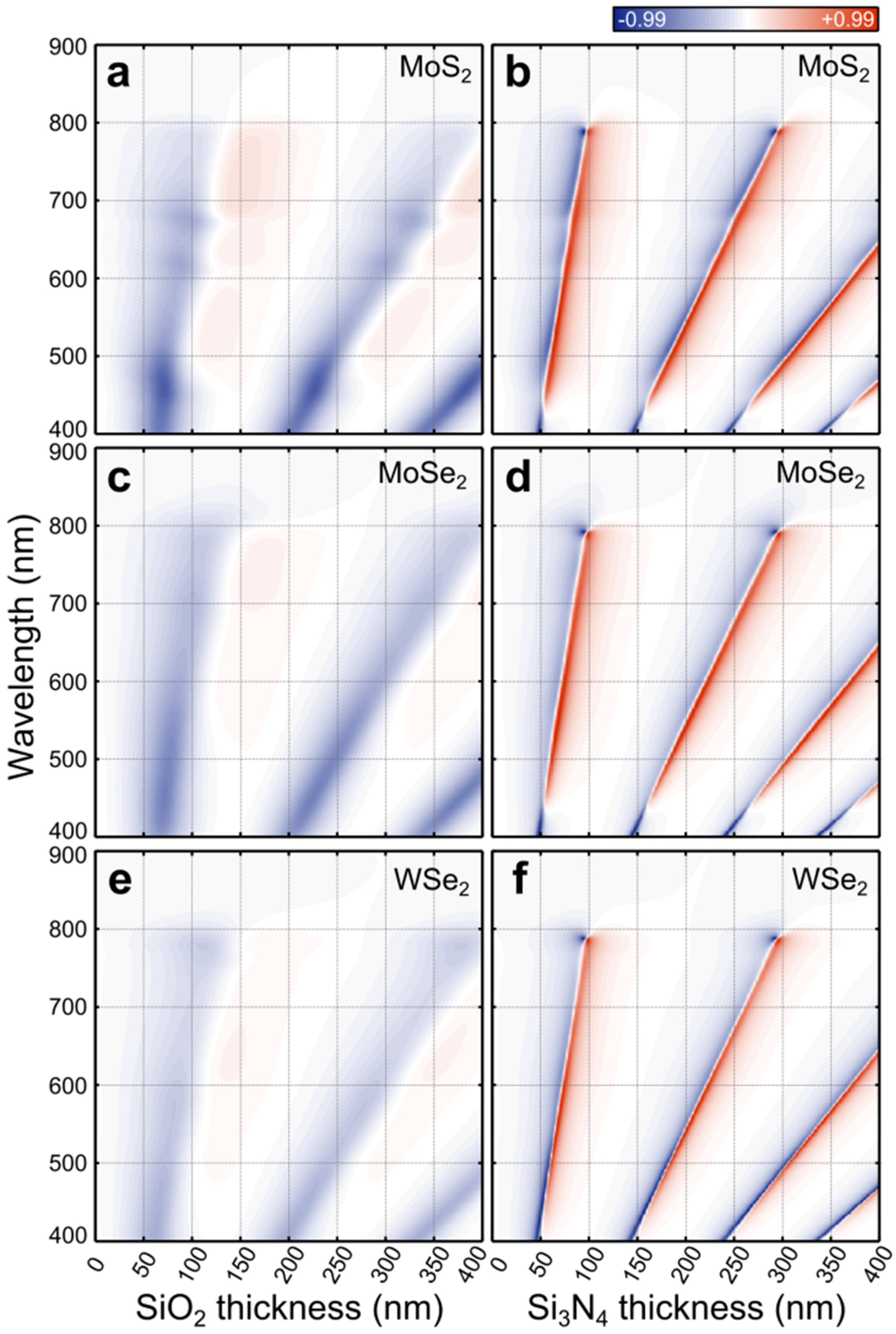
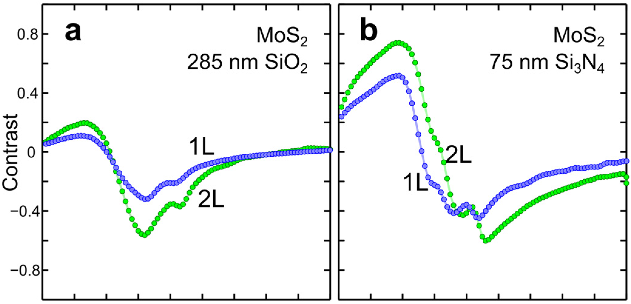
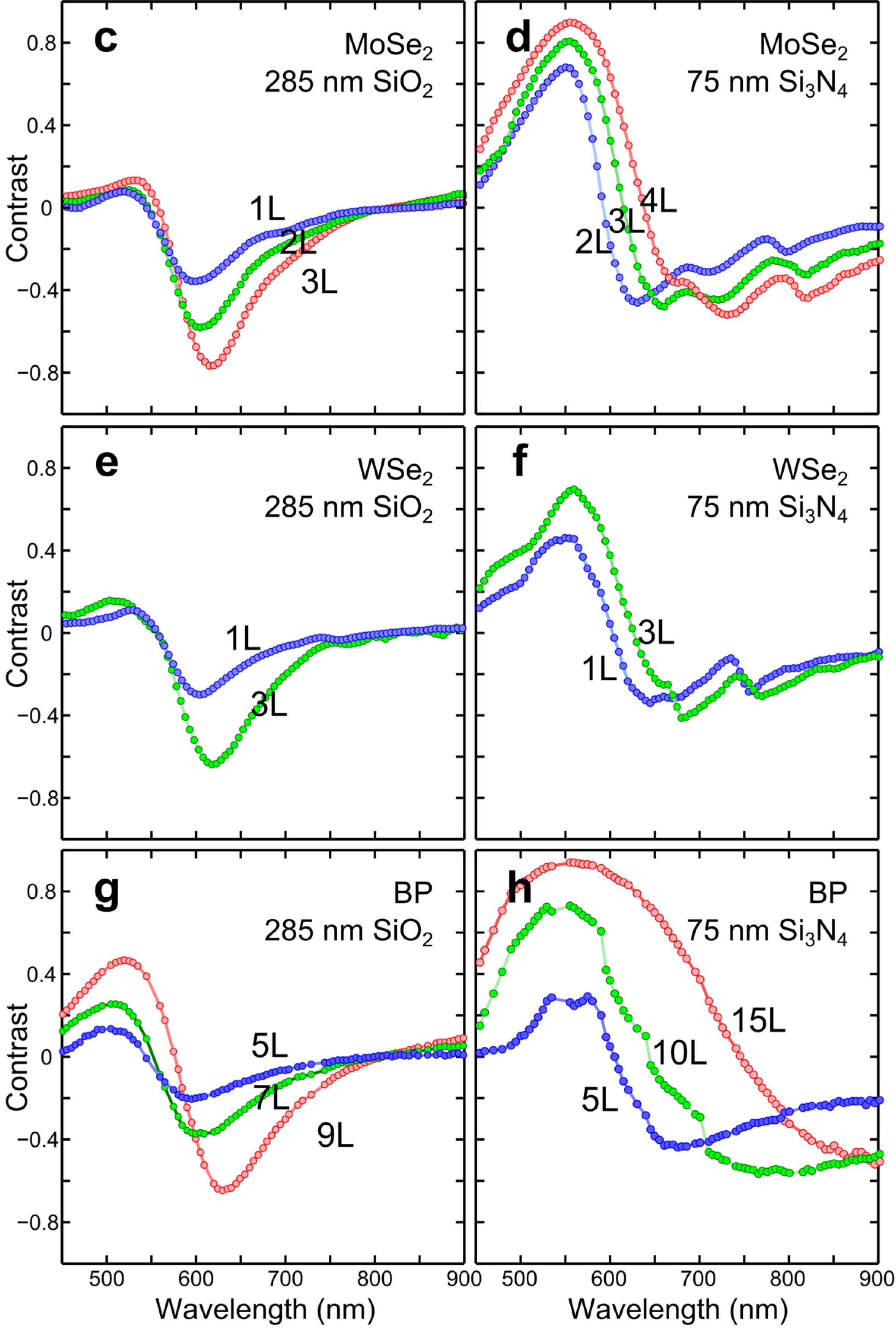
3.1. Optical Contrast Calculation

In order to evaluate the potential of Si3N4 to enhance the optical visibility of 2D semiconductors we have first calculated the optical contrast of monolayer MoS2, MoSe2 and WSe2 as function of the illumination wavelength for substrates with Si3N4 and SiO2 layers of different thickness. The model is based on the Fresnel law and more details can be found in the literature [2,3,22,23,24,25]. Briefly, the optical contrast of atomically thin materials is due to a combination of: (1) interference between the reflection paths that originate from the interfaces between the different media and (2) thickness dependent transparency of the 2D material that strongly modulates the relative amplitude of the different reflection paths. These two effects combined lead to color shifts (dependent on the thickness of the 2D material) that can be appreciated by eye. Figure 1 displays colormaps that represent the optical contrast (defined as C = (IflakeIsubstrate)/(Iflake + Isubstrate)) as a function of the illumination wavelength (vertical axis) and the thickness of the dielectric layer (horizontal axis). The references employed to extract the refractive indexes for the different materials employed in the calculation of the optical contrast are summarized in Table 1. One can clearly see how the optical contrast for Si3N4 substrates is much higher than for SiO2. Moreover, substrates with a 75 nm Si3N4 layer have a maximum contrast at a wavelength around 550 nm, which is optimal for human eye detection. The strong optical contrast enhancement observed for 75 nm thick Si3N4 layers on Si substrates can be easily understood as the combination of thickness and refractive index of this layer makes it an almost perfect anti-reflective coating. An optimal anti-reflective coating should have a refractive index n a r = n a i r n S i 2 (very similar to the nSi3N4 in the visible part of the spectrum) and a thickness d a r = λ 4 n a r 65 75 n m (to minimize the reflection within the visible part of the spectrum). In fact, the reflectivity of a 75 nm thick Si3N4 layer on Si is almost zero in the visible range of spectrum. Therefore, the contrast of the 2D materials is enhanced, because their surrounding substrate almost does not reflect any light.
Table 1. Summary of the references with the refractive index values necessary for the calculation of the optical contrast.
MaterialReference
SiO2[26]
Si3N4[27]
MoS2[28]
MoSe2[28]
WSe2[29]
Figure 1. Calculated optical contrast as a function of the illumination wavelength and spacer layer thickness for monolayer MoS2 (a,b), MoSe2 (c,d) and WSe2 (e,f) for substrates with SiO2 (left panel) and Si3N4 (right panel) spacer layers.
Electronics 04 00847 g001
As one can see from Figure 1, the optical contrast on Si3N4/Si substrates is more sensitive to small variations of the spacing layer than the SiO2/Si substrates. While for SiO2/Si substrates can present the SiO2 thickness variations of ~±10 nm, the Si3N4 layer thickness should present variations within ~±3 nm to avoid substantial contrast variations within the sample. We address the readers to the Supporting Information to see a comparison between two horizontal linecuts along 550 nm wavelength in panel (a) and (b).
The result of the calculations displayed in Figure 1 illustrates the potential of Si3N4 spacer layers with a thickness of 50 nm–100 nm to enhance the optical contrast significantly with respect to conventionally used SiO2 spacer layers. Therefore, we have explored the potential of Si3N4 in 2D semiconductor research by experimentally studying the optical contrast of several 2D semiconductors (MoS2, MoSe2, WSe2 and black phosphorus) on silicon substrates with a 75 nm thick Si3N4 layer (IDB Technologies Ltd, Whitley, Wiltshire, UK). We also fabricated samples on Si/SiO2 substrates with 285 nm SiO2 in order to compare the measured optical contrast with the most extended dielectric layer used in 2D materials research nowadays.

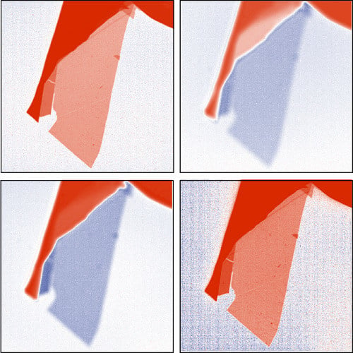
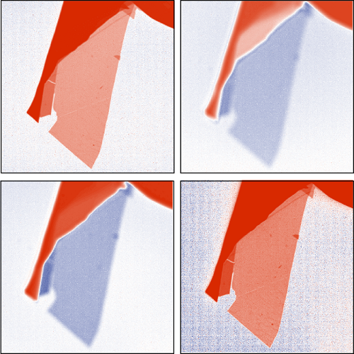
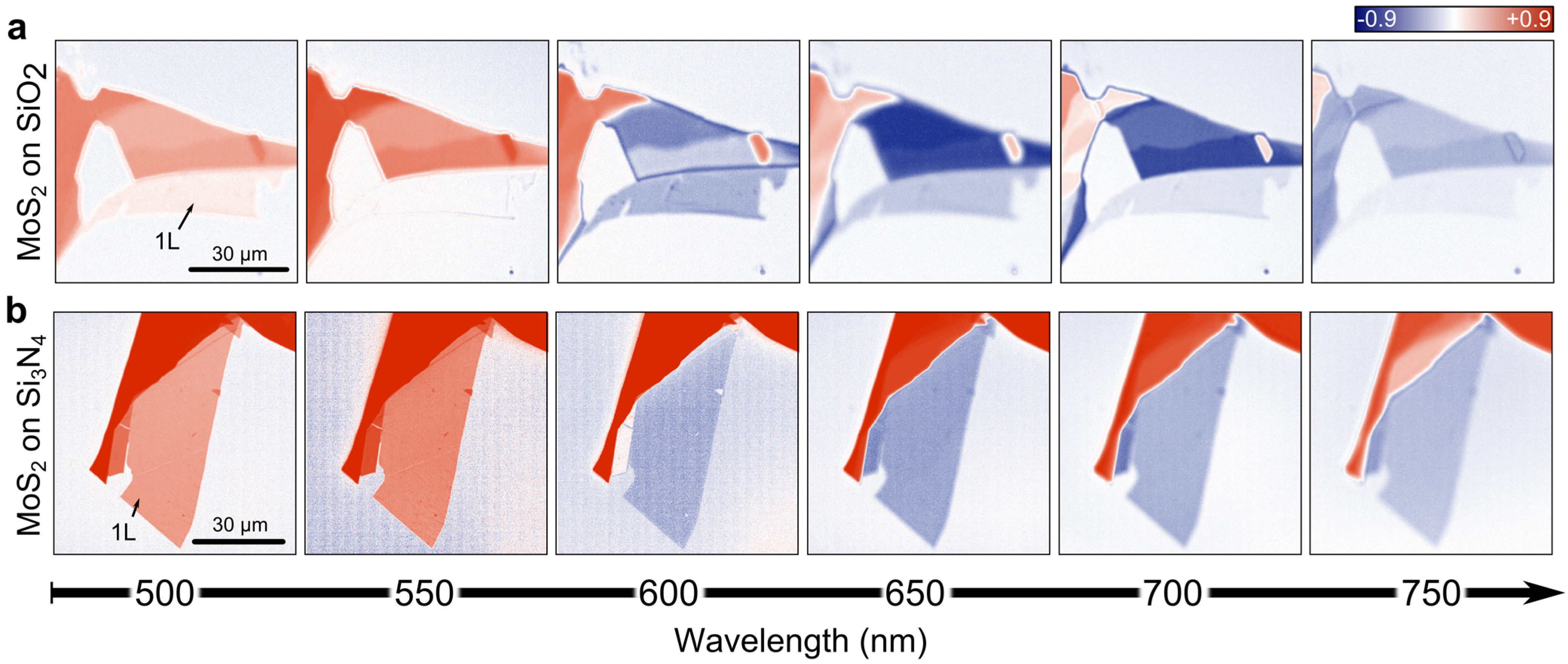
3.2. Hyperspectral Imaging

The optical contrast is measured at different illumination wavelengths with a modified hyperspectral imaging setup described in Reference [21]. The sample is illuminated with monochromatic light with the help of a monochromator. The measurement is carried out by sweeping the illumination wavelength from 450 nm to 900 nm in 5 nm steps, and acquiring an image with a monochrome camera at each wavelength step. The thickness of the studied flakes has been determined by atomic force microscopy prior to the hyperspectral imaging measurements (see Figure 2). Raman spectroscopy or photoluminescence can be also used to characterize and to determine the thickness of the exfoliated flakes on Si3N4 surfaces [30], see Supporting Information for Raman spectra acquired for MoS2 flakes on a 75 nm Si3N4/Si substrate and a comparison with the spectra reported for flakes on 285 nm SiO2/Si substrates [31,32].
Figure 2. (a) Contrast map of a MoS2 flake deposited onto a 75 nm Si3N4/Si substrate under illumination with 550 nm wavelength; (b) Topographic atomic force microscopy image acquired on the region highlighted with the square in (a), a topographic line profile is also shown below.
Electronics 04 00847 g002
Figure 3 shows the obtained optical contrast maps of MoS2 flakes with a single-layer region (highlighted in the Figure with “1 L”) on a 285 nm SiO2/Si substrate (a) and on a 75 nm Si3N4/Si substrate (b) under illumination with different wavelengths: 500 nm, 550 nm, 600 nm, 650 nm, 700 nm and 750 nm. The comparison between the results obtained for the SiO2 and Si3N4 layers illustrates how the optical contrast of monolayer MoS2 on SiO2 is weaker within the visible part of the spectrum, whereas for Si3N4 around 500–600 nm the monolayer contrast reaches the highest value.
Figure 3. Contrast maps obtained by hyperspectral imaging of MoS2 flakes on Si substrate with spacer layers of, (a) 285 nm of SiO2 or (b) 75 nm of Si3N4, at different illuminating wavelengths. The contrast in the single layer case is maximum at 550 nm for Si3N4, whereas in the SiO2 case is at 600 nm. It allows for the direct identification of single layer flakes.
Electronics 04 00847 g003

3.3. Wavelength Dependent Optical Contrast

From the contrast maps at different wavelengths one can extract the wavelength dependence of the optical contrast for flakes with different thicknesses. Figure 4 summarizes the contrast vs. wavelength dependence measured for MoS2, MoSe2, WSe2 and black phosphorus on both substrates. For all the studied materials the optical contrast is enhanced on substrates with Si3N4 by a 50%–100%. The wavelength with the maximum optical contrast is also shifted: while on SiO2/Si substrates it is ~650 nm, on Si3N4 the maximum contrast is at ~550 nm.
Figure 4. Wavelength dependence of the optical contrast measured for MoS2, MoSe2, WSe2 and black phosphorus flakes of different thickness. (a,b) optical contrast of MoS2 on 285 nm SiO2/Si and 75 nm Si3N4/Si, respectively; (c,d) optical contrast of MoSe2 on 285 nm SiO2/Si and 75 nm Si3N4/Si, respectively; (e,f) optical contrast of WSe2 on 285 nm SiO2/Si and 75 nm Si3N4/Si, respectively; (g,h) optical contrast of black phosphorus on 285 nm SiO2/Si and 75 nm Si3N4/Si, respectively.
Electronics 04 00847 g004aElectronics 04 00847 g004b

4. Conclusions

In summary, we have explored the use of Si3N4 as dielectric layer for 2D semiconductor research. We systematically studied the optical contrast of several 2D semiconductors (MoS2, MoSe2, WSe2 and black phosphorus) on silicon substrates with 75 nm of Si3N4 spacer layers, which according to our calculations should substantially enhance the optical contrast. We experimentally demonstrated the optical contrast enhancement due to 75 nm Si3N4/Si substrates by measuring the optical contrast in the range of 450 nm to 900 nm by hyperspectral imaging. We compared the measured contrast to that acquired for samples fabricated on the standard 285 nm SiO2/Si substrates, finding an increase of the optical contrast up to a 50%–100%. The maximum contrast also shifts in wavelength towards wavelength values optimal for human eye detection. The obtained results provide a way of improving optical identification of single layers of 2D materials.

Acknowledgments

A.C.-G. acknowledges financial support from the BBVA Foundation through the fellowship “I Convocatoria de Ayudas Fundacion BBVA a Investigadores, Innovadores y Creadores Culturales”, from the MINECO (Ramón y Cajal 2014 program, RYC-2014-01406) and from the MICINN (MAT2014-58399-JIN). R.G. acknowledges financial support from the AMAROUT-Marie Curie program. We also acknowledge funding from the projects MAT2014-57915-R (MINECO) and MAD2D project S2013/MIT-3007 (Comunidad Autónoma de Madrid).

Author Contributions

G.R.-B. developed the experimental setup. R.G., D.P.D.L., L.V.-G. and A.C.-G. fabricated the samples. J.Q. performed the AFM characterization. G.R.-B., R.G., D.P.D.L., L.V.-G. carried out the hyperspectral measurements. A.C.-G. directed the research project and wrote the manuscript. All authors discussed the data and interpretation, and contributed during the writing of the manuscript. All authors have given approval to the final version of the manuscript.

Conflicts of Interest

The authors declare no conflict of interest.

References

  1. Novoselov, K.S.; Jiang, D.; Schedin, F.; Booth, T.J.; Khotkevich, V.V.; Morozov, S.V.; Geim, A.K. Two-dimensional atomic crystals. Proc. Natl. Acad. Sci. USA 2005, 102, 10451–10453. [Google Scholar] [CrossRef] [PubMed]
  2. Blake, P.; Hill, E.W.; Castro Neto, A.H.; Novoselov, K.S.; Jiang, D.; Yang, R.; Booth, T.J.; Geim, A.K. Making graphene visible. Appl. Phys. Lett. 2007, 91. [Google Scholar] [CrossRef]
  3. Abergel, D.S.L.; Russell, A.; Fal’ko, V.I. Visibility of graphene flakes on a dielectric substrate. Appl. Phys. Lett. 2007, 91, 063125. [Google Scholar] [CrossRef]
  4. Casiraghi, C.; Hartschuh, A.; Lidorikis, E.; Qian, H.; Harutyunyan, H.; Gokus, T.; Novoselov, K.S.; Ferrari, A.C. Rayleigh imaging of graphene and graphene layers. Nano Lett. 2007, 7, 2711–2717. [Google Scholar] [CrossRef] [PubMed] [Green Version]
  5. Ni, Z.H.; Wang, H.M.; Kasim, J.; Fan, H.M.; Yu, T.; Wu, Y.H.; Feng, Y.P.; Shen, Z.X. Graphene thickness determination using reflection and contrast spectroscopy. Nano Lett. 2007, 7, 2758–2763. [Google Scholar] [CrossRef] [PubMed]
  6. Roddaro, S.; Pingue, P.; Piazza, V.; Pellegrini, V.; Beltram, F. The optical visibility of graphene: Interference colors of ultrathin graphite on SiO2. Nano Lett. 2007, 7, 2707–2710. [Google Scholar] [CrossRef] [PubMed]
  7. Wang, Q.H.; Kalantar-Zadeh, K.; Kis, A.; Coleman, J.N.; Strano, M.S. Electronics and optoelectronics of two-dimensional transition metal dichalcogenides. Nat. Nanotechnol. 2012, 7, 699–712. [Google Scholar] [CrossRef] [PubMed]
  8. Butler, S.Z.; Hollen, S.M.; Cao, L.; Cui, Y.; Gupta, J.A.; Gutiérrez, H.R.; Heinz, T.F.; Hong, S.S.; Huang, J.; Ismach, A.F.; et al. Progress, challenges, and opportunities in two-dimensional materials beyond graphene. ACS Nano 2013, 7, 2898–2926. [Google Scholar] [CrossRef] [PubMed]
  9. Koppens, F.H.L.; Mueller, T.; Avouris, P.; Ferrari, A.C.; Vitiello, M.S.; Polini, M. Photodetectors based on graphene, other two-dimensional materials and hybrid systems. Nat. Nanotechnol. 2014, 9, 780–793. [Google Scholar] [CrossRef] [PubMed]
  10. Buscema, M.; Island, J.O.; Groenendijk, D.J.; Blanter, S.I.; Steele, G.A.; van der Zant, H.S.J.; Castellanos-Gomez, A. Photocurrent generation with two-dimensional van der Waals semiconductors. Chem. Soc. Rev. 2015, 44, 3691–3718. [Google Scholar] [CrossRef] [PubMed]
  11. Castellanos-Gomez, A. Black phosphorus: narrow gap, wide applications. J. Phys. Chem. Lett. 2015, 6, 4280–4291. [Google Scholar] [CrossRef]
  12. Wald, G. Human Vision and the Spectrum. Science 1945, 101, 653–658. [Google Scholar] [CrossRef] [PubMed]
  13. Ponomarenko, L.A.; Yang, R.; Mohiuddin, T.M.; Katsnelson, M.I.; Novoselov, K.S.; Morozov, S.V.; Zhukov, A.A.; Schedin, F.; Hill, E.W.; Geim, A.K. Effect of a High-κ Environment on Charge Carrier Mobility in Graphene. Phys. Rev. Lett. 2009, 102, 206603. [Google Scholar] [CrossRef] [PubMed] [Green Version]
  14. Perea-López, N.; Lin, Z.; Pradhan, N.R.; Iñiguez-Rábago, A.; Laura Elías, A.; McCreary, A.; Lou, J.; Ajayan, P.M.; Terrones, H.; Balicas, L.; et al. CVD-grown monolayered MoS 2 as an effective photosensor operating at low-voltage. 2D Mater. 2014, 1, 011004. [Google Scholar] [CrossRef]
  15. Xia, J.; Huang, X.; Liu, L.-Z.; Wang, M.; Wang, L.; Huang, B.; Zhu, D.-D.; Li, J.-J.; Gu, C.-Z.; Meng, X.-M. CVD synthesis of large-area, highly crystalline MoSe2 atomic layers on diverse substrates and application to photodetectors. Nanoscale 2014, 6, 8949–8955. [Google Scholar] [CrossRef] [PubMed]
  16. Van der Zande, A.M.; Huang, P.Y.; Chenet, D.A.; Berkelbach, T.C.; You, Y.; Lee, G.-H.; Heinz, T.F.; Reichman, D.R.; Muller, D.A.; Hone, J.C. Grains and grain boundaries in highly crystalline monolayer molybdenum disulphide. Nat. Mater. 2013, 12, 554–561. [Google Scholar] [CrossRef] [PubMed]
  17. Torrisi, F.; Hasan, T.; Wu, W.; Sun, Z.; Lombardo, A.; Kulmala, T.S.; Hsieh, G.-W.; Jung, S.; Bonaccorso, F.; Paul, P.J.; et al. Inkjet-printed graphene electronics. ACS Nano 2012, 6, 2992–3006. [Google Scholar] [CrossRef] [PubMed]
  18. Li, J.; Naiini, M.M.; Vaziri, S.; Lemme, M.C.; Östling, M. Inkjet Printing of MoS 2. Adv. Funct. Mater. 2014, 24, 6524–6531. [Google Scholar] [CrossRef]
  19. Withers, F.; Yang, H.; Britnell, L.; Rooney, A.P.; Lewis, E.; Felten, A.; Woods, C.R.; Sanchez Romaguera, V.; Georgiou, T.; Eckmann, A.; et al. Heterostructures produced from nanosheet-based inks. Nano Lett. 2014, 14, 3987–3992. [Google Scholar] [CrossRef] [PubMed]
  20. Castellanos-Gomez, A.; Buscema, M.; Molenaar, R.; Singh, V.; Janssen, L.; van der Zant, H.S.J.; Steele, G.A. Deterministic transfer of two-dimensional materials by all-dry viscoelastic stamping. 2D Mater. 2014, 1, 011002. [Google Scholar] [CrossRef]
  21. Castellanos-Gomez, A.; Quereda, J.; van der Meulen, H.P.; Agraït, N.; Rubio-Bollinger, G. Spatially resolved optical absorption spectroscopy of single- and few-layer MoS2 by hyperspectral imaging. arXiv 2015, 1507.00869. Available online: http://arxiv.org/abs/1507.00869 (accessed on 3 July 2015). [Google Scholar]
  22. Castellanos-Gomez, A.; Agraït, N.; Rubio-Bollinger, G. Optical identification of atomically thin dichalcogenide crystals. Appl. Phys. Lett. 2010, 96, 213116. [Google Scholar] [CrossRef]
  23. Li, H.; Lu, G.; Yin, Z.; He, Q.; Li, H.; Zhang, Q.; Zhang, H. Optical Identification of Single- and Few-Layer MoS2 Sheets. Small 2012, 8, 682–686. [Google Scholar] [CrossRef] [PubMed]
  24. Li, H.; Wu, J.; Huang, X.; Lu, G.; Yang, J.; Lu, X.; Xiong, Q.; Zhang, H. Rapid and reliable thickness identification of two-dimensional nanosheets using optical microscopy. ACS Nano 2013, 7, 10344–10353. [Google Scholar] [CrossRef] [PubMed]
  25. Dols-Perez, A.; Sisquella, X.; Fumagalli, L.; Gomila, G. Optical visualization of ultrathin mica flakes on semitransparent gold substrates. Nanoscale Res. Lett. 2013, 8, 305. [Google Scholar] [CrossRef] [PubMed] [Green Version]
  26. Jung, I.; Pelton, M.; Piner, R.; Dikin, D.A.; Stankovich, S.; Watcharotone, S.; Hausner, M.; Ruoff, R.S. Simple Approach for High-Contrast Optical Imaging and Characterization of Graphene-Based Sheets. Nano Lett. 2007, 7, 3569–3575. [Google Scholar] [CrossRef]
  27. Refractive index of Si3N4. Available online: www.filmetrics.com (accessed on 1 August 2015).
  28. Beal, A.R.; Hughes, H.P. Kramers-Kronig analysis of the reflectivity spectra of 2H-MoS 2, 2H-MoSe 2 and 2H-MoTe 2. J. Phys. C Solid State Phys. 1979, 12, 881–890. [Google Scholar] [CrossRef]
  29. Beal, A.R.; Liang, W.Y.; Hughes, H.P. Kramers-Kronig analysis of the reflectivity spectra of 3R-WS 2 and 2H-WSe 2. J. Phys. C Solid State Phys. 1976, 9, 2449–2457. [Google Scholar] [CrossRef]
  30. Tóvári, E.; Csontos, M.; Kriváchy, T.; Fürjes, P.; Csonka, S. Characterization of SiO2/SiNx gate insulators for graphene based nanoelectromechanical systems. Appl. Phys. Lett. 2014, 105, 123114. [Google Scholar] [CrossRef]
  31. Lee, C.; Yan, H.; Brus, L.E.; Heinz, T.F.; Hone, Ќ.J.; Ryu, S. Anomalous Lattice Vibrations of Single-and Few-Layer MoS2. ACS Nano 2010, 4, 2695–2700. [Google Scholar] [CrossRef] [PubMed]
  32. Buscema, M.; Steele, G.A.; van der Zant, H.S.J.; Castellanos-Gomez, A. The effect of the substrate on the Raman and photoluminescence emission of single-layer MoS2. Nano Res. 2014, 7, 561–571. [Google Scholar] [CrossRef]

