
Low Power High-Efficiency Shift Register Using Implicit Pulse-Triggered Flip-Flop in 130 nm CMOS Process for a Cryptographic RFID Tag

Abstract
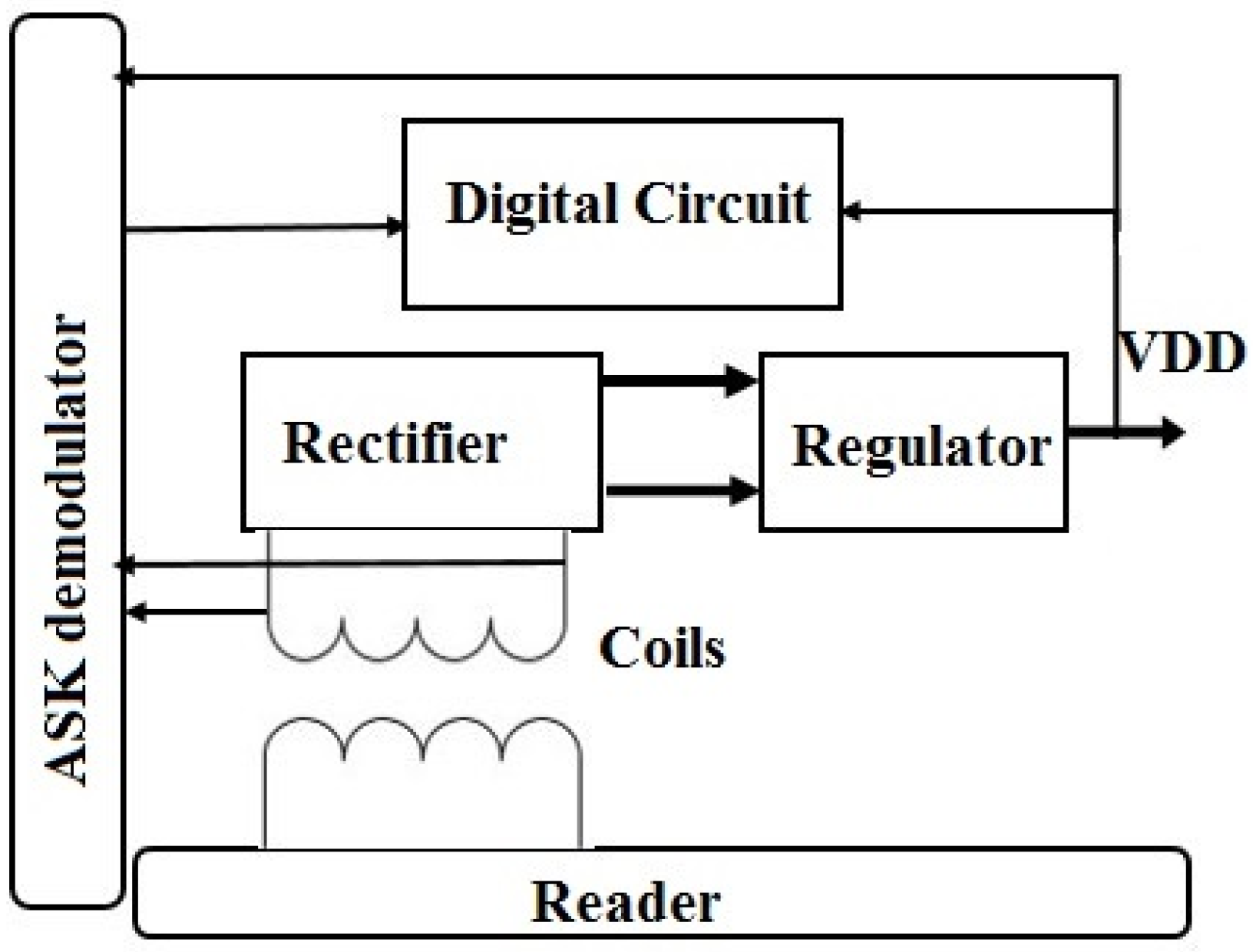
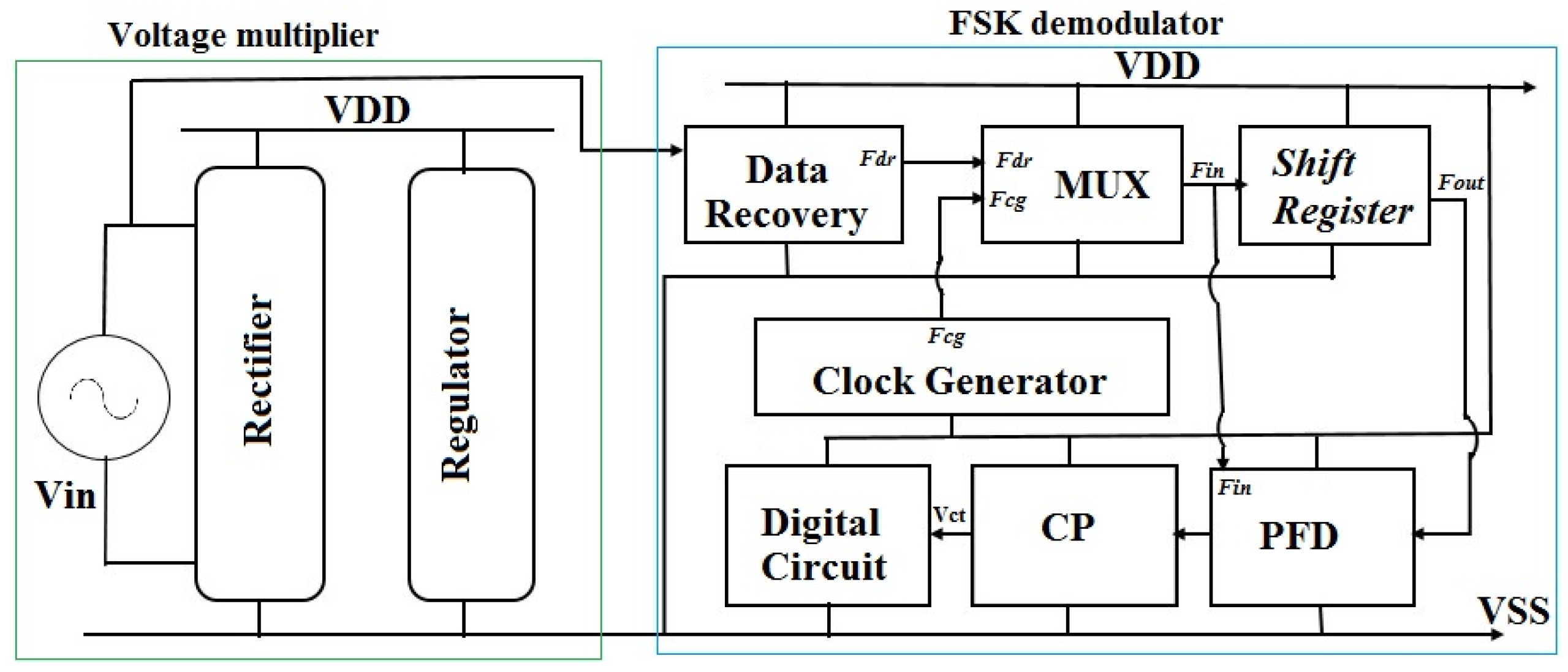
:1. Introduction
2. Methodology
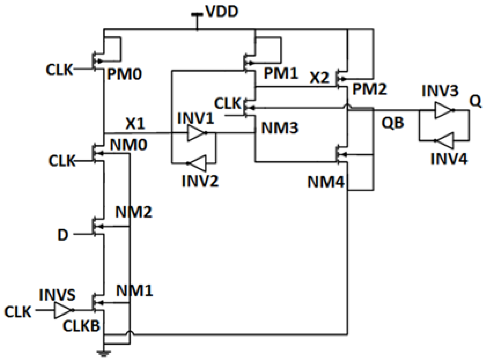
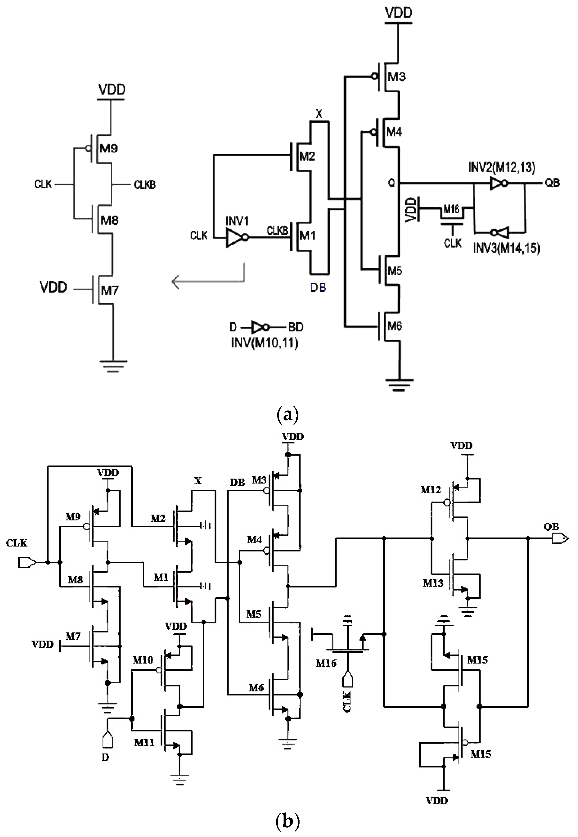
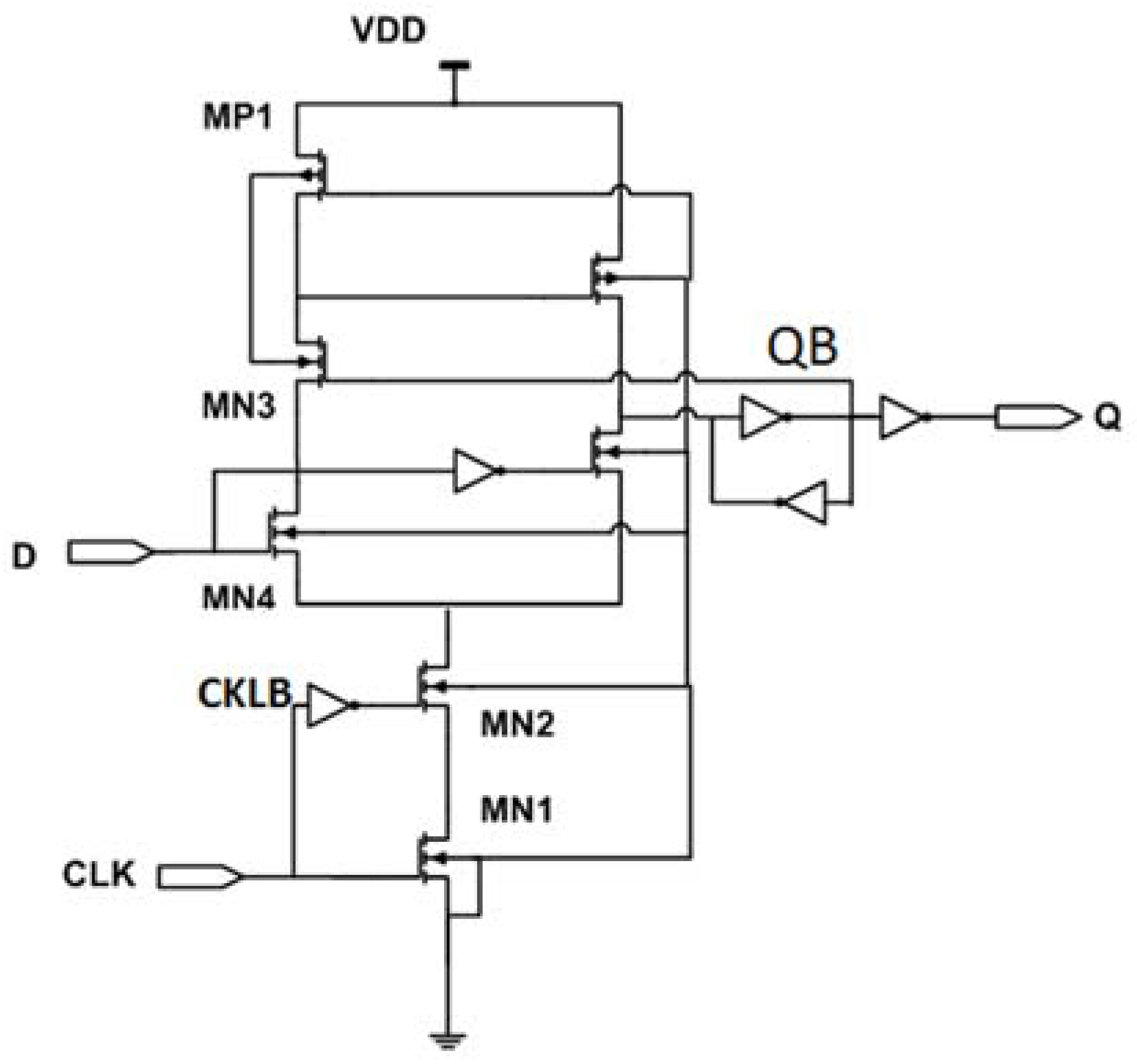
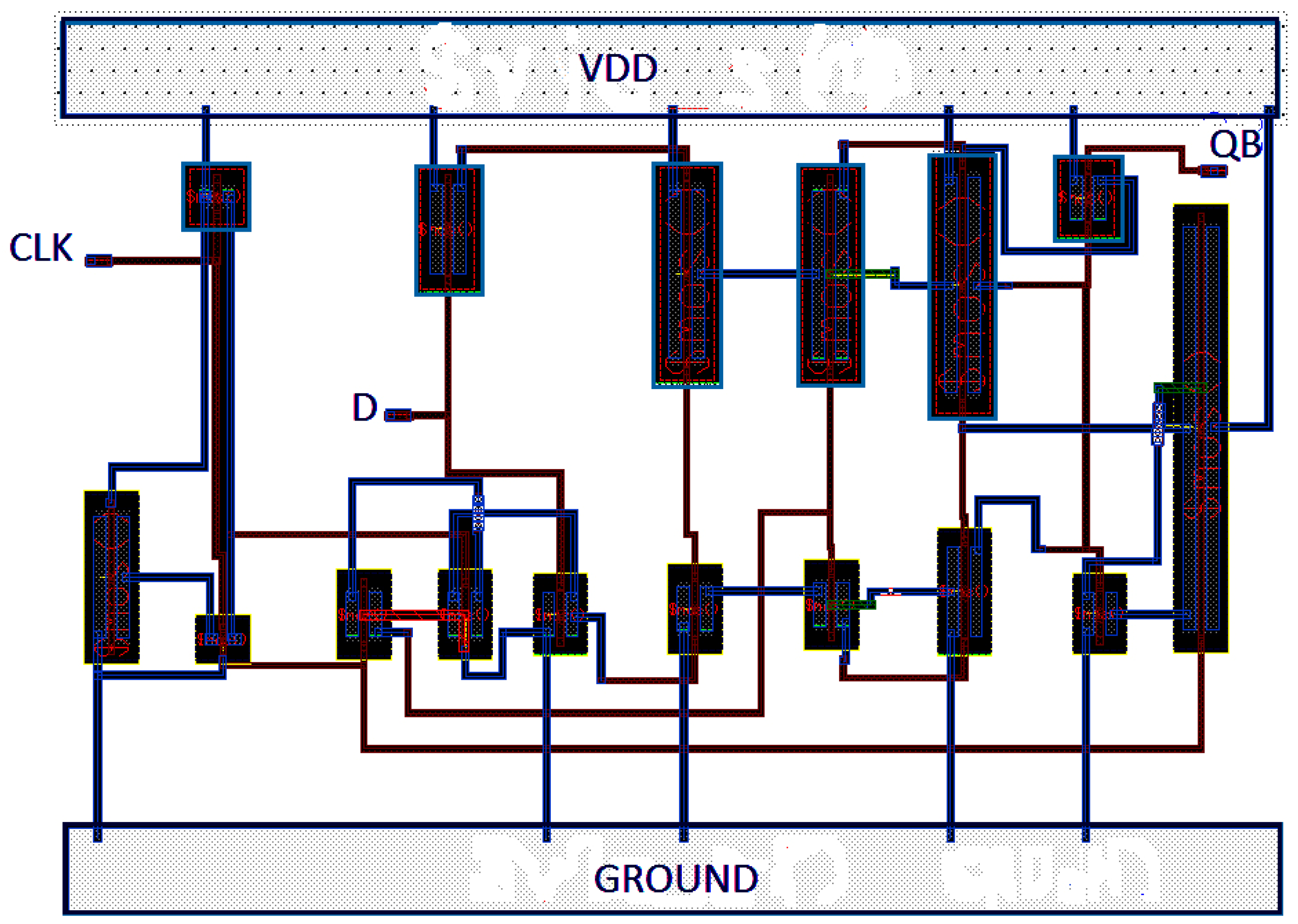
2.1. Proposed FF Design
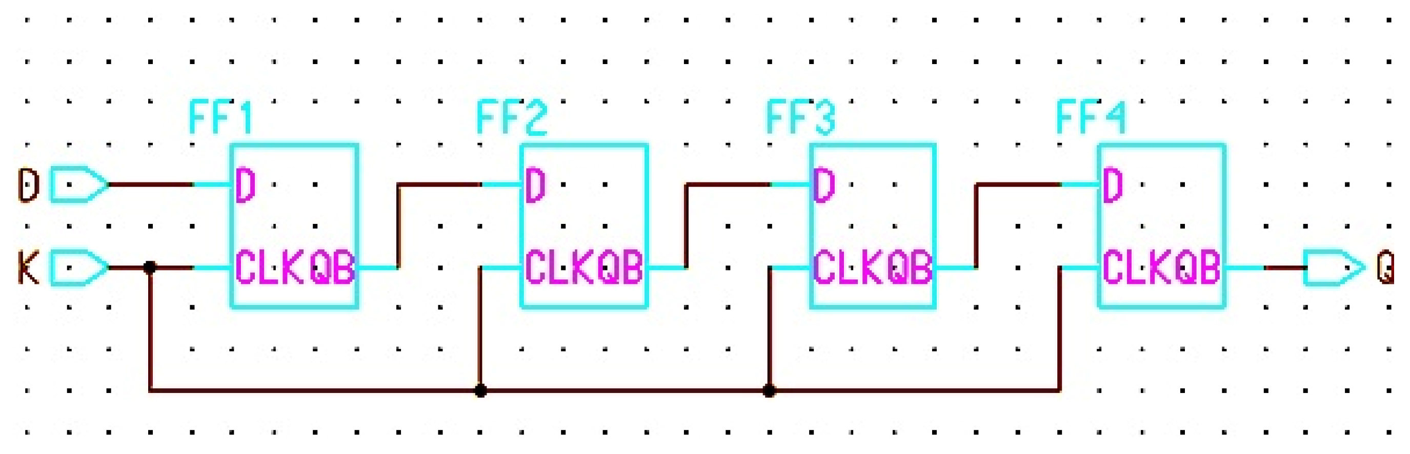
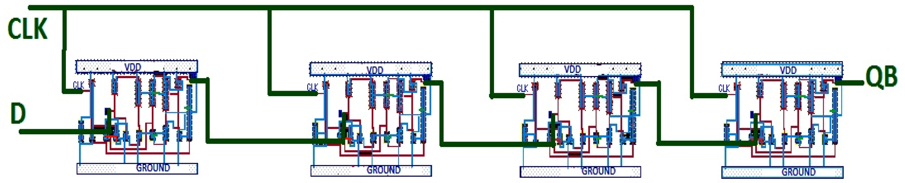
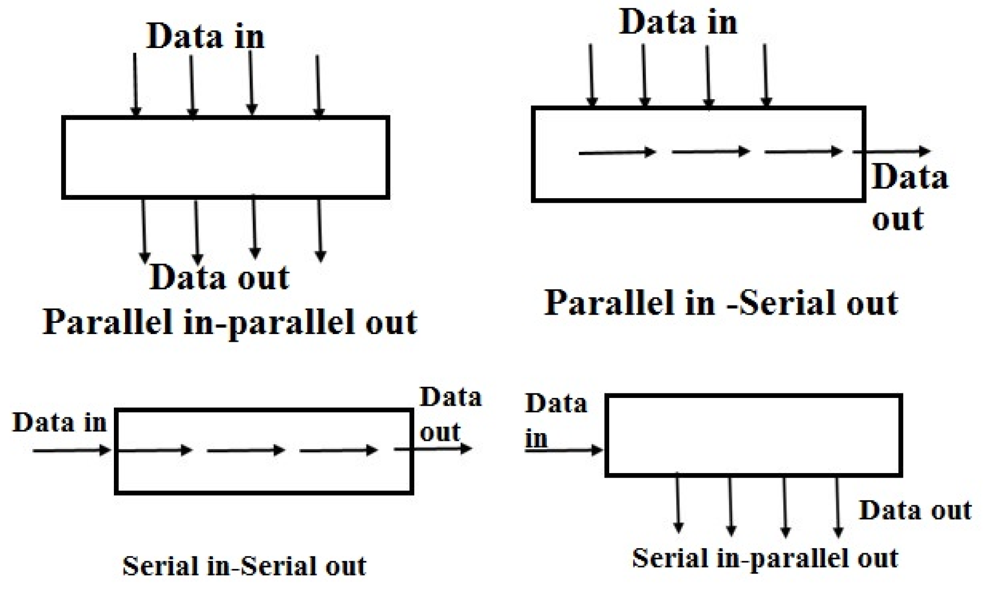
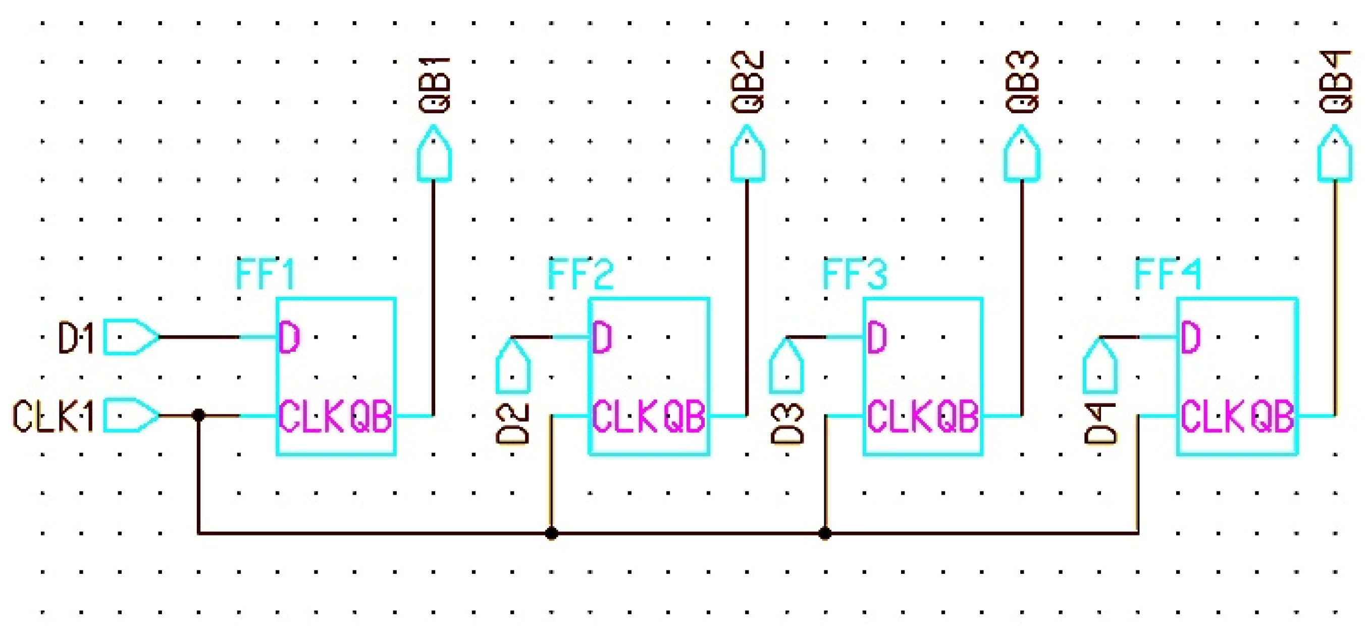
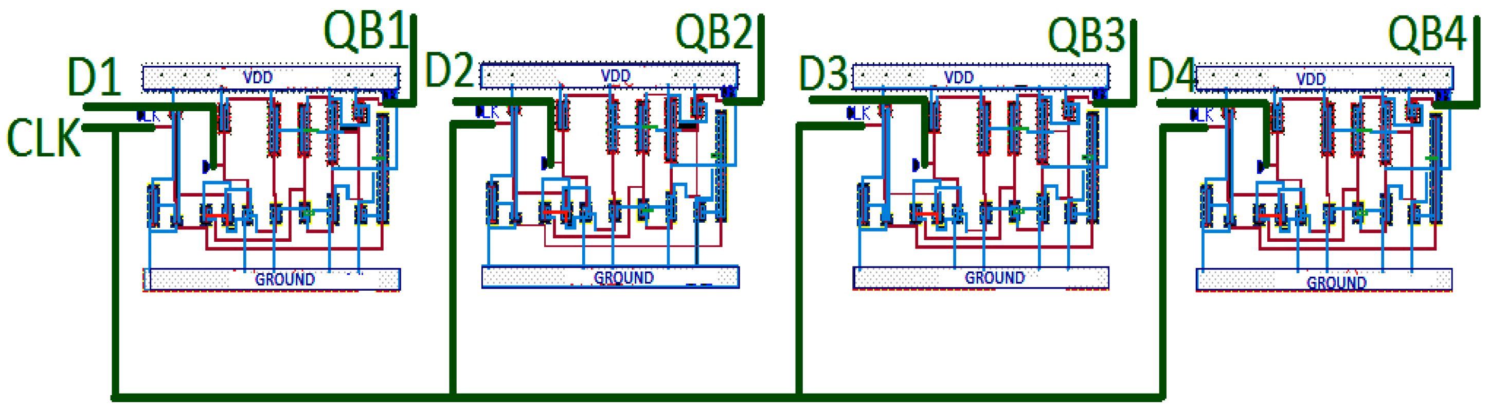
2.2. Proposed Shift Register Design
3. Results and Discussion
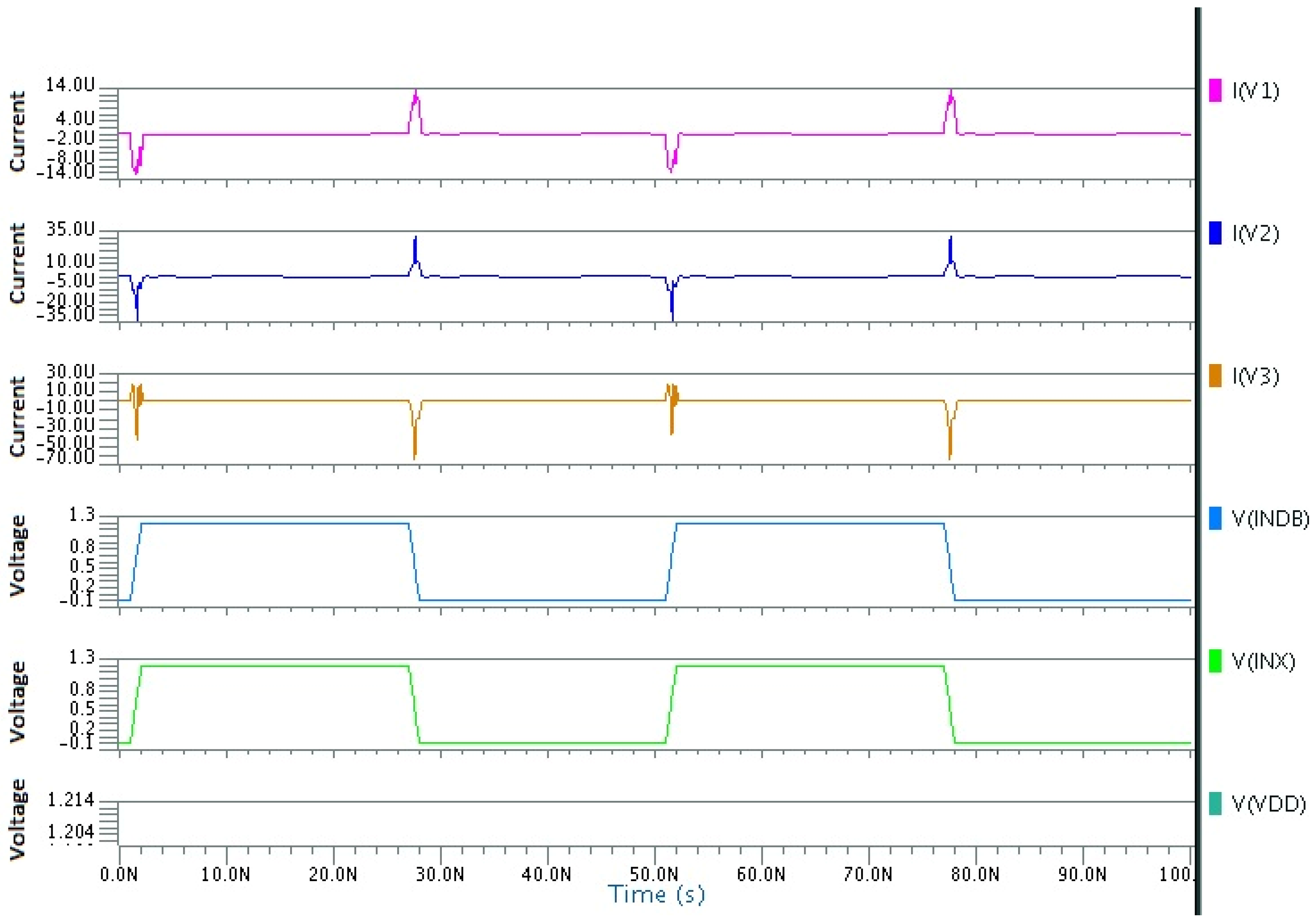
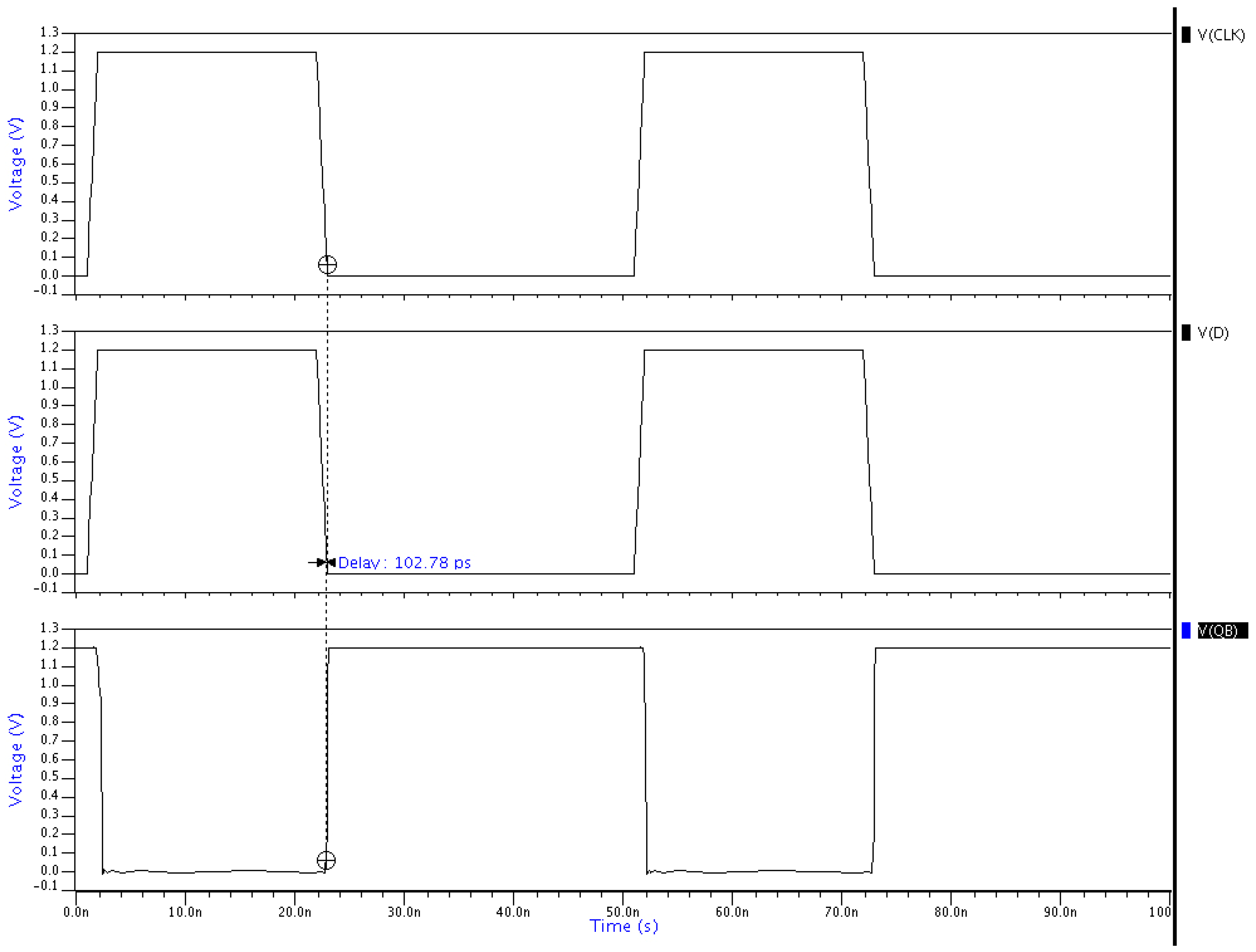
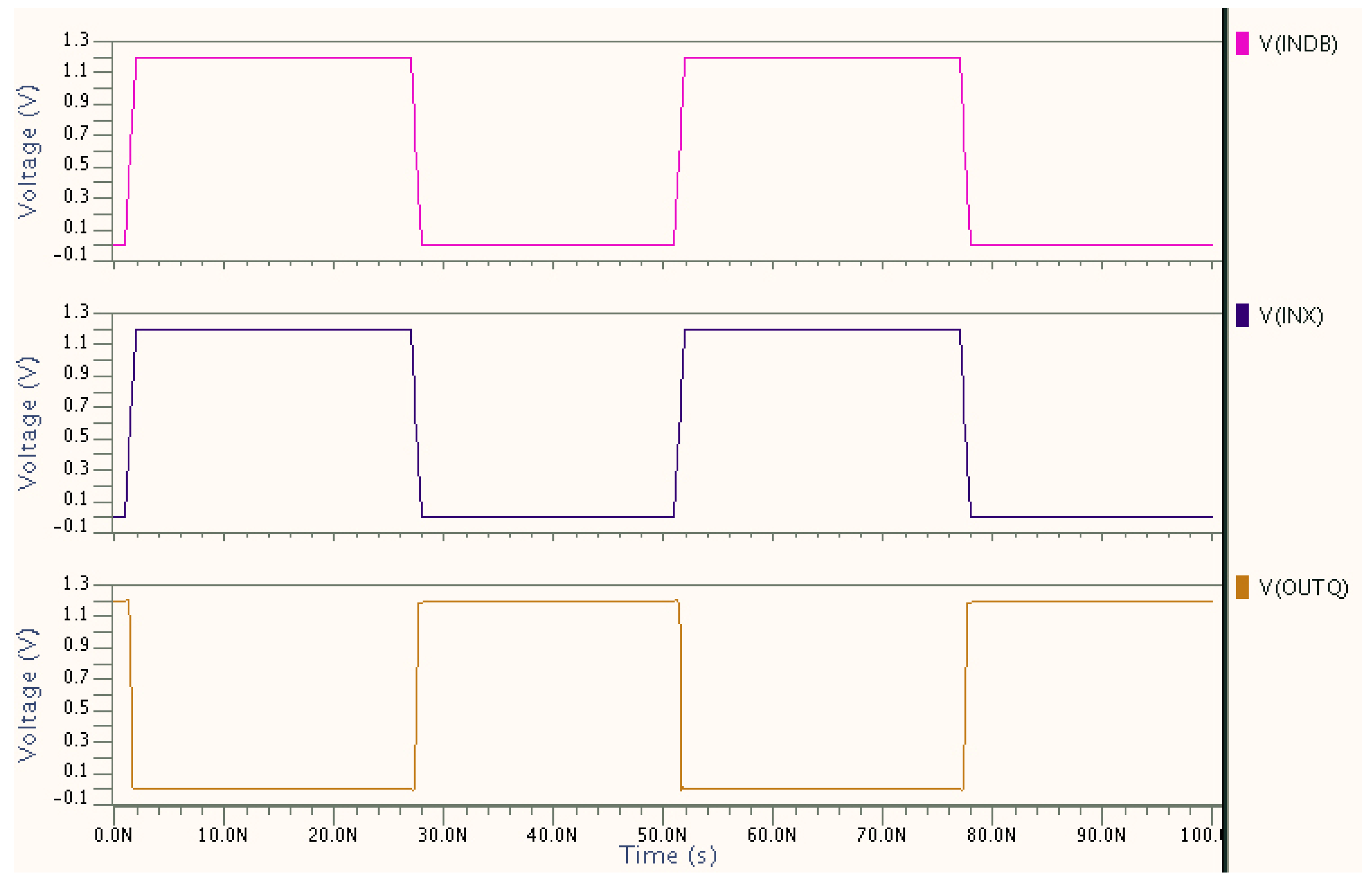
3.1. Flip-Flop
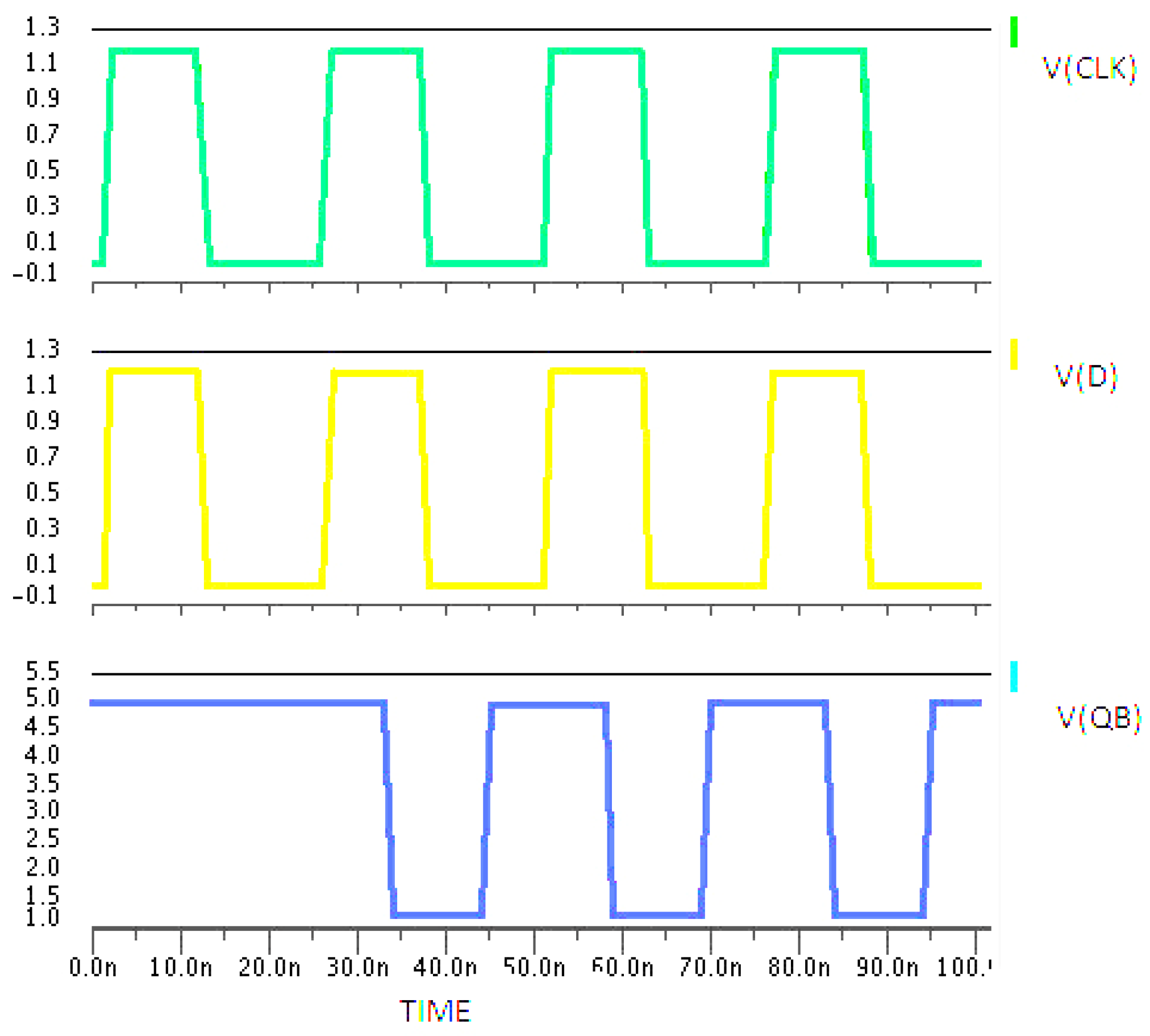
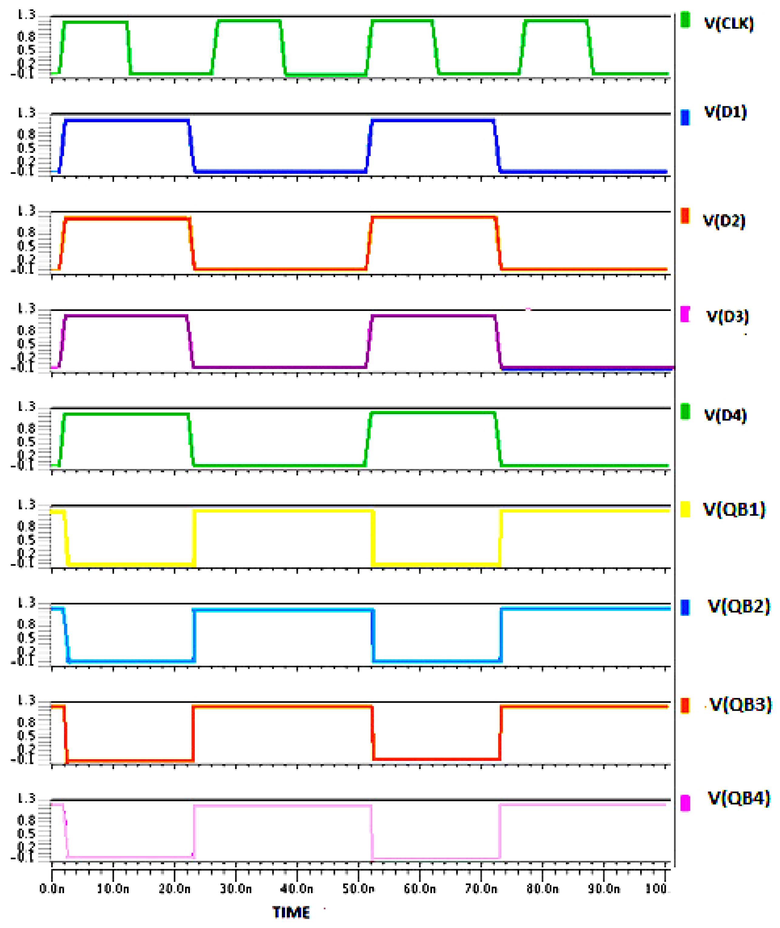
3.2. PIPO and SISO Shift Registers
4. Conclusions
Author Contributions
Conflicts of Interest
References
- De Smedt, V.; Gielen, G.; Dehaene, W. Design of a low-power wireless rfid tag. In Temperature- and Supply Voltage-Independent Time References for Wireless Sensor Networks; Springer: University of Leuven, Heverlee, Belgium, 2015; pp. 295–305. [Google Scholar]
- Chen, J.; Miyaj, A.; Sato, H.; Su, C. Improved lightweight pseudo-random number generators for the low-cost rfid tags. In Proceedings of the IEEE Trustcom/BigDataSE/ISPA, Helsinki, Finland, 20–22 August 2015; pp. 17–24.
- Spiekermann, S.; Evdokimov, S. Critical rfid privacy-enhancing technologies. IEEE Secur. Priv. 2009, 2, 56–62. [Google Scholar] [CrossRef]
- Albert, B.B.; de Assis, F.; Rodrigues, M.V. Single shift-register for rfid tag secrecy. In Proceedings of the IEEE International Telecommunications Symposium-ITS 2010, Campina Grande, Brazil, 28–31 March 2010.
- Bhuiyan, M.A.S.; Reaz, M.B.I.; Badal, M.T.I.; Mukit, M.A.; Kamal, N. Design of an Active Inductor-Based T/R Switch in 0.13 μm CMOS Technology for 2.4 GHz RF Transceivers. Trans. Electr. Electron. Mater. 2016, 17, 261–269. [Google Scholar] [CrossRef]
- Benssalah, M.; Djeddou, M.; Drouiche, K. Design and implementation of a new active RFID authentication protocol based on elliptic curve encryption. In Proceedings of the IEEE SAI Computing Conference (SAI), London, UK, 13–15 July 2016; pp. 1076–1081.
- Nohl, K.; Evans, D.; Starbug, S.; Plötz, H. Reverse-Engineering a Cryptographic RFID Tag. In Proceedings of the 17th USENIX Security Symposium, San Jose, CA, USA, 28 July–1 August 2008.
- Yuh-Shyan, H.; Ho, C.L. A New CMOS Analog Front End for RFID Tags. IEEE Trans. Ind. Electron. 2009, 56. [Google Scholar] [CrossRef]
- Kim, Y.W.; Kim, J.-S.; Kim, J.-W.; Kong, B.-S. CMOS differential logic family with conditional operation for low-power application. IEEE Trans. Circuits Syst. II Express Briefs 2008, 55, 437–441. [Google Scholar]
- Loveless, T.; Jagannathan, S.; Reece, T.; Chetia, J.; Bhuva, B.; McCurdy, M.; Massengill, L.; Wen, S.-J.; Wong, R.; Rennie, D. Neutron-and proton-induced single event upsets for d-and dice-flip/flop designs at a 40 nm technology node. IEEE Trans. Nucl. Sci. 2011, 58, 1008–1014. [Google Scholar] [CrossRef]
- Lee, Y.K.; Sakiyama, K.; Batina, L.; Verbauwhede, I. Elliptic-curve-based security processor for RFID. IEEE Trans. Comput. 2008, 57, 1514–1527. [Google Scholar] [CrossRef]
- Sarbishei, O.; Maymandi-Nejad, M. A novel overlap-based logic cell: An efficient implementation of flip-flops with embedded logic. IEEE Trans. Very Large Scale Integr. VLSI Syst. 2010, 18, 222–231. [Google Scholar] [CrossRef]
- Katti, R.; Ruan, X.; Khattri, H. Multiple-output low-power linear feedback shift register design. IEEE Trans. Circuits Syst. Regul. Pap. 2006, 53, 1487–1495. [Google Scholar] [CrossRef]
- Phyu, M.W.; Fu, K.; Goh, W.L.; Yeo, K.-S. Power-efficient explicit-pulsed dual-edge triggered sense-amplifier flip-flops. IEEE Trans. Very Large Scale Integr. VLSI Syst. 2011, 19, 1–9. [Google Scholar] [CrossRef]
- Kawaguchi, H.; Sakurai, T. A reduced clock-swing flip-flop (rcsff) for 63% power reduction. IEEE J. Solid State Circuits 1998, 33, 807–811. [Google Scholar] [CrossRef]
- Zhao, P.; McNeely, J.; Kuang, W.; Wang, N.; Wang, Z. Design of sequential elements for low power clocking system. IEEE Trans. Very Large Scale Integr. VLSI Syst. 2011, 19, 914–918. [Google Scholar] [CrossRef]
- Blanco, J.; Garcia, A.; Pastor, J.M.; Canas, V.; Morenas, J.D.L. Ultra-lightweight algorithm for generating pseudo-random number sequences in passive UHF-RFID tags. In Proceedings of the ITG-Fachbericht-Smart SysTech 2016, Duisburg, Germany, 7–8 July 2016.
- Mahmoodi, H.; Tirumalashetty, V.; Cooke, M.; Roy, K. Ultra-low power clocking scheme using energy recovery and clock gating. IEEE Trans. Very Large Scale Integr. VLSI Syst. 2009, 17, 33–44. [Google Scholar] [CrossRef]
- Absel, K.; Manuel, L.; Kavitha, R.K. Low-power dual dynamic node pulsed hybrid flip-flop featuring efficient embedded logic. IEEE Trans. Very Large Scale Integr. VLSI Syst. 2013, 21, 1693–1704. [Google Scholar] [CrossRef]
- Shams, M.; Ebergen, J.C.; Elmasry, M.I. Modeling and comparing CMOS implementations of the C-element. IEEE Trans. Very Large Scale Integr. VLSI Syst. 1998, 6, 563–567. [Google Scholar] [CrossRef]
- Shakeri, M.; Mamun, M.; Labonnah, F.R.; Fzida, H.H. Design and optimization of the power consumption in 16 bits shift register using single edge triggered d flip-flop. J. Eng. Appl. Sci. 2013, 8, 38–43. [Google Scholar]
- Rampriya, R.; Marutharaj, T. Power Efficient Design of Sequential Circuits using OBSC and RTPG Integration. Int. J. Comput. Sci. Mob. Comput. 2013, 2, 268–278. [Google Scholar]
- Jayaprakash, C.H.; Surendra Babu, V.; Indira, T.; Premkumar, M. Design and Analysis 4 Bit Shift Register Using Low Power Pulse Triggered Flip-Flop. Int. J. Electron. Commun. Technol. 2014, 5, l–3. [Google Scholar]
- Arunlakshman, M. Power and delay analysis of double edge triggered D-Flip Flop based shift registers in 16nm MOSFET technology. Int. J. Adv. Res. Electr. Electron. Instrum. Eng. 2014, 3, 8560–8568. [Google Scholar]


| FF Designs | Proposed FF | SCCER [18] | DDFF [19] |
|---|---|---|---|
| Technology (CMOS) | 130 nm | 250 nm | 90 nm |
| Number of transistors | 16 | 17 | 18 |
| Supply voltage | 1.2 V | 2.5 V | 1.2 V |
| Total power | 7.5499 nw | 83.88 µw | 205.42 µw |
| Minimum delay | 102.78 ps | 285.9 ps | 166 ps |
| Shift Registers | Proposed PIPO | PIPO Using OBSC and RTPG FF [22] | PIPO Using EPTL FF [23] | PIPO USING D-FF [24] |
|---|---|---|---|---|
| Technology (CMOS) | 130 nm | 90 nm | 50 nm | 16 nm |
| Number of transistors | 64 | - | 68 | - |
| Supply voltage | 1.2 V | 1 V | - | 0.7 V |
| Total power | 30.1997 nw | 52.997 µw | 5.51 µw | 748 µw |
| Minimum delay | 102.78 ps | 105 ps | - | 1013.5 ps |
© 2016 by the authors; licensee MDPI, Basel, Switzerland. This article is an open access article distributed under the terms and conditions of the Creative Commons Attribution (CC-BY) license (http://creativecommons.org/licenses/by/4.0/).
Share and Cite
Badal, M.T.I.; Reaz, M.B.I.; Jalil, Z.; Bhuiyan, M.A.S. Low Power High-Efficiency Shift Register Using Implicit Pulse-Triggered Flip-Flop in 130 nm CMOS Process for a Cryptographic RFID Tag. Electronics 2016, 5, 92. https://doi.org/10.3390/electronics5040092
Badal MTI, Reaz MBI, Jalil Z, Bhuiyan MAS. Low Power High-Efficiency Shift Register Using Implicit Pulse-Triggered Flip-Flop in 130 nm CMOS Process for a Cryptographic RFID Tag. Electronics. 2016; 5(4):92. https://doi.org/10.3390/electronics5040092
Chicago/Turabian StyleBadal, Mohammad Torikul Islam, Mamun Bin Ibne Reaz, Zinah Jalil, and Mohammad Arif Sobhan Bhuiyan. 2016. "Low Power High-Efficiency Shift Register Using Implicit Pulse-Triggered Flip-Flop in 130 nm CMOS Process for a Cryptographic RFID Tag" Electronics 5, no. 4: 92. https://doi.org/10.3390/electronics5040092