
Photonic Structure-Integrated Two-Dimensional Material Optoelectronics

1
Department of Electrical Engineering and Computer Science, Vanderbilt University, Nashville, TN 37235-1824, USA
2
Department of Physics and Astronomy, Vanderbilt University, Nashville, TN 37235-1807, USA
*
Author to whom correspondence should be addressed.
Electronics 2016, 5(4), 93; https://doi.org/10.3390/electronics5040093
Submission received: 25 October 2016
/
Revised: 5 December 2016
/
Accepted: 9 December 2016
/
Published: 20 December 2016
(This article belongs to the Special Issue Two-Dimensional Electronics and Optoelectronics)
Abstract
:The rapid development and unique properties of two-dimensional (2D) materials, such as graphene, phosphorene and transition metal dichalcogenides enable them to become intriguing candidates for future optoelectronic applications. To maximize the potential of 2D material-based optoelectronics, various photonic structures are integrated to form photonic structure/2D material hybrid systems so that the device performance can be manipulated in controllable ways. Here, we first introduce the photocurrent-generation mechanisms of 2D material-based optoelectronics and their performance. We then offer an overview and evaluation of the state-of-the-art of hybrid systems, where 2D material optoelectronics are integrated with photonic structures, especially plasmonic nanostructures, photonic waveguides and crystals. By combining with those photonic structures, the performance of 2D material optoelectronics can be further enhanced, and on the other side, a high-performance modulator can be achieved by electrostatically tuning 2D materials. Finally, 2D material-based photodetector can also become an efficient probe to learn the light-matter interactions of photonic structures. Those hybrid systems combine the advantages of 2D materials and photonic structures, providing further capacity for high-performance optoelectronics.
1. Introduction
Two-dimensional (2D) materials have attracted extensive attention since the last century due to the wealth of novel physical properties when charge and heat transport are confined to the direction perpendicular to a 2D plane. The isolation of graphene in 2004 by Geim and Novoselov first showed the possibility to obtain stable, single-atom layer 2D materials from their van der Waals solids [1]. In the past decade, graphene has been demonstrated to possess many outstanding merits not only for thermal and mechanical applications, but also for electronics and optoelectronics [2,3,4,5,6,7,8,9,10]. The great success of graphene encourages researchers to rediscover and restudy other 2D materials [11,12,13,14,15]. One of the most well-studied 2D material families is transition metal dichalcogenide (TMDC). TMDCs have a general chemical formula of MX2, where M is a transition metal atom from groups IV, V, and VI (e.g., Mo, W), and X is a chalcogen atom (e.g., S, Se, Te) [16,17]. The variety of elements and the layer-dependence enable TMDCs to present a wide range of electrical, optical, chemical, thermal and mechanical properties [11,18,19,20,21,22,23,24,25,26]. Two distinctive features of TMDCs are strong excitonic effects and valley/spin-dependent properties. TMDCs process indirect bandgap for bulk crystals, while in the single layer limit, they become direct-bandgap semiconductors with gaps located at the K and the K’ points [18,27,28,29]. Moreover, the broken in-plane inversion symmetry in monolayer give rise to valley-dependent optical and electrical properties [24,30,31,32]. Graphene analogues are another important type of 2D material, which includes hexagonal boron nitride (hBN) with a large bandgap up to 6 eV [6,33], anisotropic black phosphorus (BP) [15,34,35,36,37,38,39], and the most recent addition, boronphene [40]. The last category of 2D materials is transition metal oxide, including titania- and perovskite-oxides. Those oxide nanosheets have exhibited great potential for new capacitors and energy-storage devices [41].
Interestingly, 2D materials present several advantages over conventional three-dimensional (3D) materials for optoelectronics. First, although the innate thinness renders these materials almost transparent, their strong light-matter interactions enable decent single-pass absorption. For example, single-layer graphene absorbs 2.3% of vertically incident white light [42]. Monolayer molybdenum disulfide (MoS2) absorbs around 10% at excitonic resonances [43]. Moreover, 2D materials cover a wide response spectral range from microwave to ultraviolet wavelengths. For instance, the zero bandgap makes graphene a potential candidate for optical applications over a broad spectral range. However, its semi-metallic nature prevents the realization of efficient optoelectronics due to a large dark current. TMDCs possess relatively larger bandgaps, enabling excellent on/off ratio, but limiting their performance in telecom-wavelength. BP has a layer-tunable direct bandgap ranging from 0.3 eV in bulk to 1.8–2.0 eV in monolayer [36], which covers from visible to mid-infrared spectral regions. Finally, the absence of dangling bonds makes 2D materials easy to be integrated with photonic structures or stacked together to form vertical van der Waals heterostructures [44].
Integrating external photonic structures with 2D material-based optoelectronics is a novel strategy to broaden the horizon of applications for 2D materials. Those metallic and dielectric photonic or nanophotonic structures can be precisely sculpted into various architectures so that light can be scattered, confined, refracted and processed in controllable ways [45,46,47]. Patterning 2D materials into arrays is a straightforward approach to form internal photonic structures. By sculpting 2D materials into plasmonic nanostructures like resonators or nanocavities, enhanced light absorption can be achieved [48,49,50,51,52]. Furthermore, external metallic plasmonic nanostructures enable light manipulation beyond the diffraction limit of light by the excitation of surface plasmons, which confines the electromagnetic field at the metal surface. Photonic waveguides provide another possibility to control light flows. With the assistance of waveguides, light can be side coupled into 2D material devices, leading to enhanced responsivity. The combination of photonic structures with 2D material-based optoelectronic devices provides the possibility to enhance the overall performance since special requirements at a certain location, polarization direction or wavelength can be achieved by choosing different photonic structures or tuning their geometric parameters. On the other hand, combining 2D material-based devices with classic photonic modulators offers an approach to tuning the modulator performance by electrostatically manipulating 2D materials. Moreover, the 2D material/photonic structures hybrid systems allow 2D material optoelectronics to become a probe to investigate light-matter interactions of photonic structures.
In this review, we will first briefly overview 2D material-based optoelectronics, especially photodetectors, and their physical mechanisms. For the purpose of this review, we broadly define 2D materials to be thin-layered films and those atomically thin layers are held together only by van der Waals force. Also, the total thicknesses of the thin films can vary from several angstroms to tens of nanometers. In the following, we will give a general discussion about the structure and performance of photonic structure/2D material hybrid systems, in which 2D optoelectronics are combined with different photonic structures, including plasmonic nanostructures, photonic waveguides and crystals. Next, we will present the possibility that 2D material optoelectronics can influence and even probe the properties of photonic structures. Finally, we will summarize the main conclusions of the review and describe the future opportunities in this promising field of research.
2. Two-Dimensional (2D) Material-Based Optoelectronics
In addition to the outstanding electronic properties of 2D materials, such as high mobility of graphene devices and high on/off ratio of TMDC-based transistors, their unique optical properties also attract researchers to learn their optoelectronic characterizations [10,17,53,54,55,56,57,58,59].
2.1. Photocurrent-Generation Mechanisms
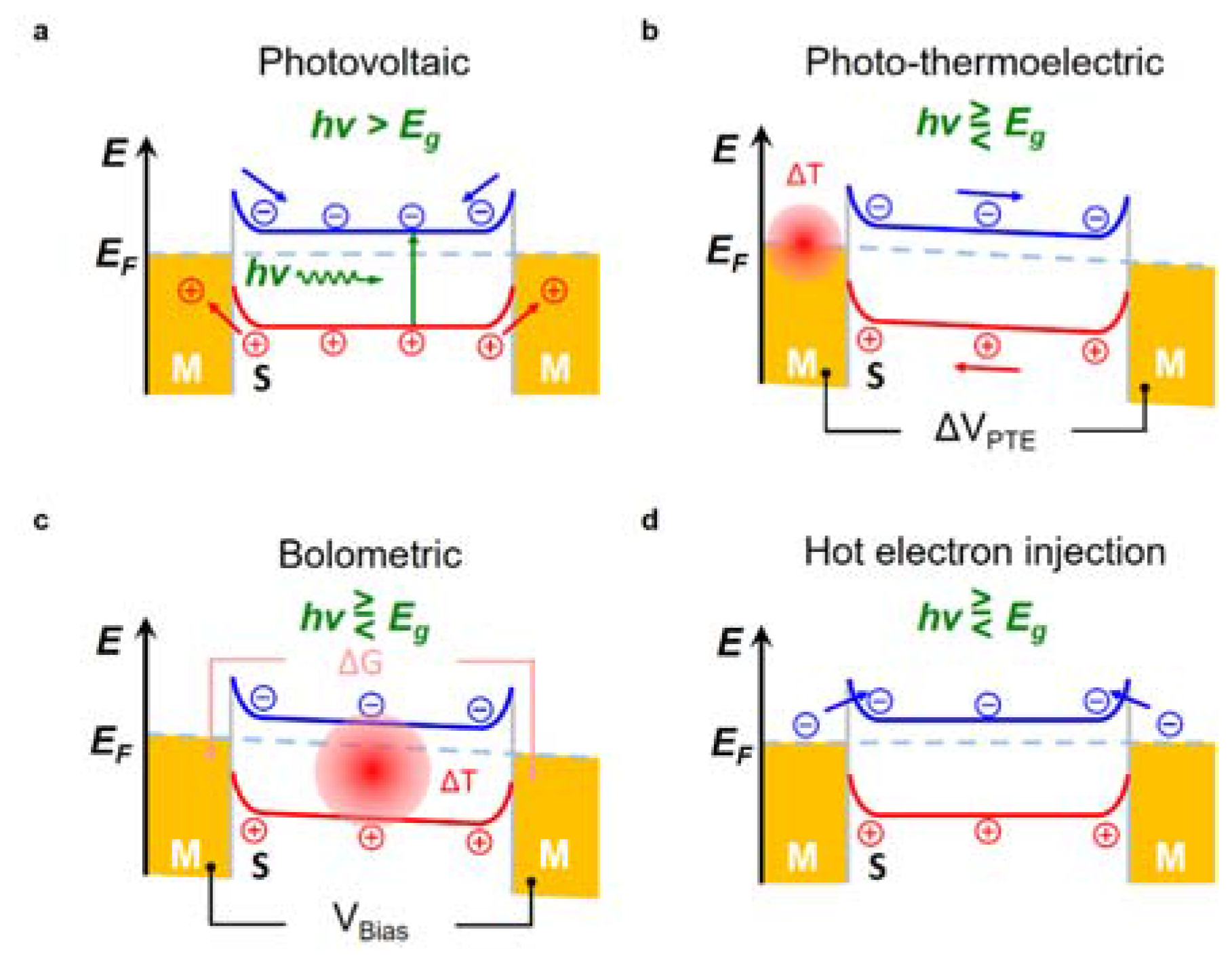
Generally, the photoresponses of 2D material-based devices can be attributed to more than one mechanism when device structures vary or are investigated under different light illumination conditions. Here, several widely studied mechanisms in typical 2D material-based optoelectronics will be described, including photovoltaic effect, photo-thermoelectric effect, photo-bolometric effect, and hot electron injection. Figure 1 summarizes these mechanisms in terms of a typical 2D material-based phototransistor, in which a 2D material thin film bridges two metal electrodes. Here we plot semiconducting 2D material channels rather than semimetal channels to show more comprehensive circumstances. Additionally, photoconductive effect and photogating can also contribute to photocurrent generation [60].
2.2. Photovoltaic Effect (PVE)
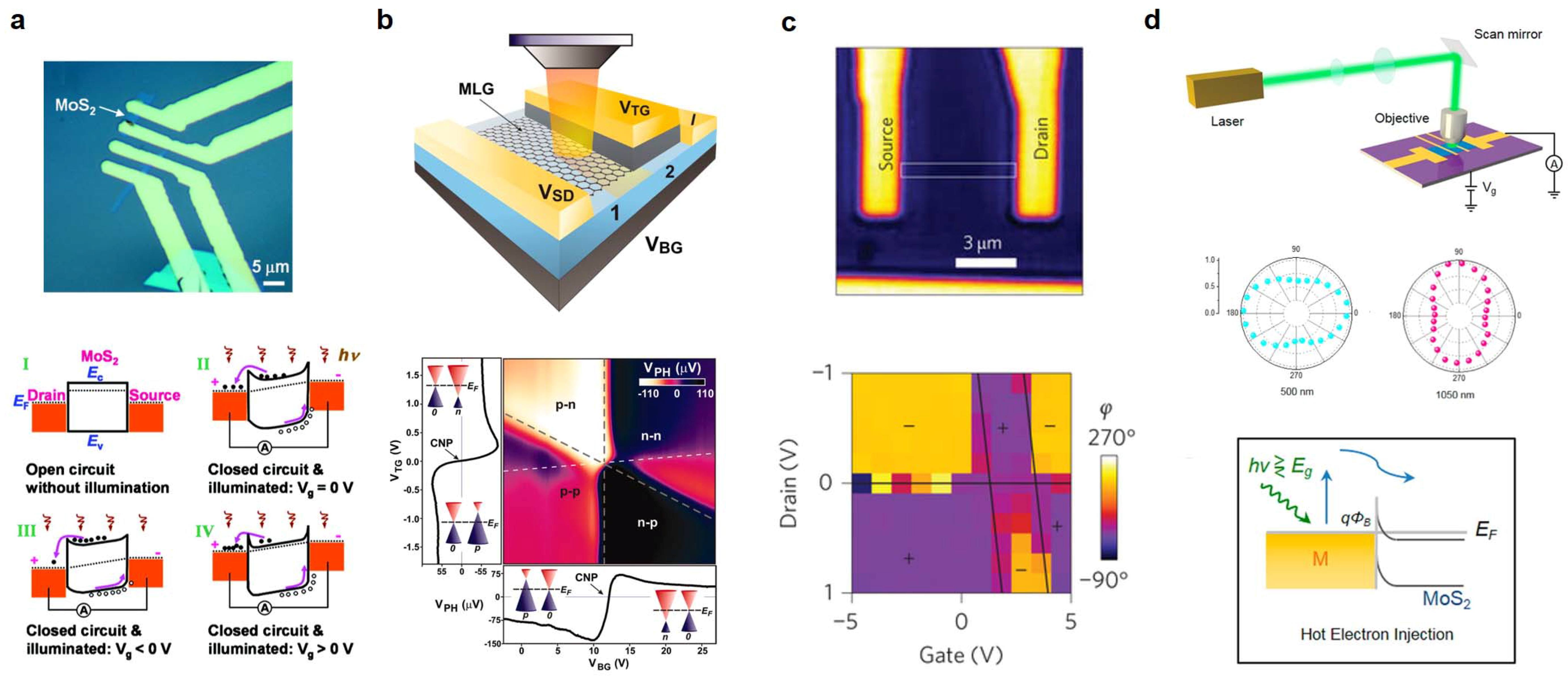
In early studies, the photocurrent generation in 2D materials is attributed to the separation of photon-excited electron-hole pairs (EHPs), usually at PN junctions or metal-semiconductor Schottky barriers, where internal electric fields force the photo-excited EHPs to be separated. This phenomenon is known as photovoltaic effect (PVE), which has been elaborated in traditional 3D semiconductor devices [61,62]. Here we note that photocurrent is defined to be . As shown in Figure 1a, under illumination with photon energy larger than the bandgap of 2D materials, electrons in the valence band can be excited to the conduction band, producing photo-excited EHPs. With the assistance of internal electric fields, excess electrons and holes will be driven to opposite directions, leading to a light-generated current (IL). When the circuit is open, the accumulation of carriers induces a voltage (open circuit voltage Voc), which lowers the potential barrier and generates a forward bias diffusion current that balances the light-generated current. If the external bias is set to be zero, the photo-excited EHPs will be collected, generating a photocurrent (short circuit current Isc). For typical graphene or 2D material-based phototransistors, PVE is thought to be dominant since Schottky barriers usually exist when 2D materials contact metal electrodes. By applying various external gate voltages on an MoS2 device, as illustrated in Figure 2a, the conduction/valence band level of single-layer MoS2 will be tuned accordingly [63]. Thus, the band alignment presents great difference under various gate voltages. Since the band alignment will directly affect the direction and value of the internal electric field, the sign and intensity of PVE-induced photocurrent will change significantly when the gate voltage is sweeping. The drain bias is also very important in terms of PVE since it provides a way to tune the lateral band alignment.
2.3. Photo-Thermoelectric Effect and Photo-Bolometric Effect
The thermal mechanisms can also drive photocurrent generation. In those cases, photo-thermoelectric effect (PTE) and photo-bolometric effect (PBE) can contribute to the photocurrent generation by inducing non-uniform heat and an overall conductance change of the 2D material channel under light illumination, respectively. Seebeck coefficient is defined as the ability to induce thermoelectric voltage in response to a temperature difference across the material and can usually be expressed through the Mott relation [64,65]:
where kB is the Boltzmann constant, G is conductance, e is the electron charge, and EF is Fermi energy. For a semiconductor channel that connected to two metal electrodes, the light-induced temperature increase (ΔT) at the metal electrodes will generate a photo-thermoelectric voltage across the channel as displayed in Figure 1b. PTE drives a current through the junction even without applying an external bias, and the current value is directly related to the channel conductance and the photo-thermoelectric voltage, which is determined by the Seebeck coefficient difference between the semiconductor channel and the metal electrodes, and the temperature change:
The Seebeck coefficients of pure metals are typically in the order of 1 μV/K. However, for 2D materials (such as graphene, TMDCs and BP), the Seebeck coefficient ranges from several to thousands μV/K [66,67,68,69,70,71,72,73]. On the other hand, as shown in Figure 1c, the local heat induced by photon absorption can modify the resistance of the channel. This light-induced conductance will lead to photocurrent under an external bias by PBE [74,75]. The PBE-induced photocurrent can be presented by the following equation:
where ΔG is the conductance change and VD is the external bias. From Equation (3), we find that the PBE-induced photocurrent is predicted to present a linear relationship to the applied bias. In previous investigations, PTE and PBE have been found to play indispensable roles in 2D material-based devices. Although PTE-induced photocurrent is negligible in the case that the illumination is focused within a uniform semiconducting channel, PTE effect can be observed for a nonuniformity doping, for instance, a graphene junction consisting of bilayer and monolayer [66]. A report by Gabor et al. further demonstrated the PTE in graphene by studying a dual-gated graphene PN junction, as presented in Figure 2b [76]. By changing the biases that were applied to the top and bottom gates, the doping level of the two sides of the junction can be precisely and independently controlled. The photoresponses exhibit six-fold polarity variation, which is attributed to the changes of the Seebeck coefficient of graphene when the gate bias varies. Additionally, PTE effect can be observed at 2D material/metal interface. A study about monolayer MoS2 transistors has reported that the photoresponse at MoS2/metal junction is dominant by PTE and demonstrated large Seebeck coefficient for MoS2 under an external electric field [71]. On the other hand, PBE has been comprehensively studied for carbon nanotube devices, in which photoresponse shows linear negative correlation to the external bias [75]. PBE-induced photocurrents have also been observed by Freitag et al. when the graphene channel is heavily doped (Figure 2c) [77], in which overall current drops under light excitation since the temperature increase leads to a reduction in carrier mobility. Similar phenomena have also been detected in heavily doped BP devices [72].
2.4. Hot Electron Injection
With further investigation of 2D material optoelectronics, hot electron injection has been demonstrated as a novel photocurrent-generation mechanism [78]. It is well-known that photon-excited hot electrons in metal electrodes can cross over the Schottky barrier and be injected into the semiconductor channel. The injection yield of electrons Y follows the Fowler equation:
where EF is the Fermi energy, is the reduced plank constant, is the incident light frequency, and is the Schottky barrier. Hot electron injection has been reported to be indispensable in TMDC-based devices, such as a MoS2-based phototransistor (Figure 2d) [78]. Anisotropic photocurrent response has been detected under illumination with photon energy below the MoS2 bandgap. More importantly, the anisotropic ratios are found to be related to the shape of Au electrodes, indicating the hot electron contribution from metal electrodes. Additionally, hot electron injection also plays an important role when 2D materials directly contact with silicon photonic crystals and metal plasmonic nanostructures [79].
For a practical device, the situation is more complex, usually present a combined effect of different mechanisms [76]. Therefore, many strategies are adopted to learning the photocurrent-generation mechanisms for various devices. Unlike graphene, TMDCs present slightly complicated scenarios due to the existence of appreciable bandgaps. For the most well-known Mo- and W-based TMDCs, bandgaps are typically ranged from 1 to 2 eV. Wavelength-dependence and polarization-dependence measurements are conducted to further probe the underlying physical mechanisms. From those studies, various photocurrent-generation mechanisms are reported under different illumination conditions [21,78,80]. Taking MoS2 as an example, when the photon energy is high enough to generate photo-excited EHPs, large photocurrent signals can be observed at junction areas because of PVE. However, measurable photocurrent signals can also be detected when incident photon energy is below the bandgap of MoS2. In this case, PTE can explain the photocurrent generation at metal electrode areas. Moreover, at metal-semiconductor junctions, photocurrent signals are detected to exhibit polarization dependency perpendicular to the metal edge, which is attributed to the hot electron injection [78].
As the investigation of photocurrent-generation mechanisms in 2D optoelectronics goes deeper, 2D material-based devices have also been demonstrated to exhibit elevated performance. Over the past decade, it has been shown that most graphene-based phototransistors exhibit photoresponsivity around 10 mA/W [9,81]. By introducing electron trapping centres, high broadband photoresponse is demonstrated to achieve 8.61 A/W [8]. Moreover, due to the high carrier mobility and high carrier-saturation velocity, graphene-based optoelectronics are reported to operate at speed up to tens of gigahertz [81]. First reported single-layer MoS2 phototransistors reach responsivity to 7.5 mA/W with 50 V gate bias, and exhibit stable response time within 50 ms [63]. An ultrasensitive monolayer MoS2 photodetector was reported later to show a maximum external photoresponsivity of 880 A/W at 561 nm [21]. Other TMDCs, such as MoSe2, WS2 and WSe2, have also been employed for optoelectronics, and achieve photoresponsivities ranging from tens of A/Ws to hundreds [82]. It must be mentioned that an electrostatically defined PN junction has been realized by locally gating the WSe2 thin film [19]. BP is a new addition to the 2D family, and it attracts tremendous attention in the optoelectronic field due to its unique optical properties, especially its anisotropic nature and layer-dependent bandgaps, which covers the visible to mid-infrared spectral range. BP-based photodetectors are reported to reach photoresponsivity up to 4.8 mA/W [39]. Additionally, due to the directional dependence of the interband transition strength in the anisotropic band structure of BP, polarized photocurrent responses are observed in BP phototransistors via PVE [83]. On the other hand, PTE and PBE-induced photocurrent generation is also considered to be important, especially in metallic or doped multilayer BP phototransistors [72].
In addition to the 2D material-based optoelectronics in the above discussions, 2D material-based heterostructures have been reported to show excellent performance for optoelectronic applications in the previous literatures [84,85,86,87,88,89]. By stacking different 2D semiconducting crystals on top of each other with van der Waals-like forces, those heterostructures are expected to show combined functionality of the individual layers and new phenomena at the interface. For example, a maximum photodetection responsivity of 418 mA/W at the wavelength of 633 nm has been achieved by stacking p-type BP with n-type MoS2 to form ultrathin PN diodes [90]. The photocurrent signals at the PN junction are much stronger than photoresponse at the metal-semiconductor contacts due to the large band mismatch at the heterojunction. The polarization direction of the photoresponse at the junction is affected by either BP or MoS2 channel, depending on the illumination conditions [91]. Moreover, 2D material-based heterostructures allow the possibility to obtain high quality devices by encapsulating a 2D material thin film with 2D insulators such as hBN sheets to form a sandwich-like structure. The hBN sheets provide an ultra-smooth surface for the inner graphene film and protect the graphene film from direct exposure to air or contact with substrates. These devices exhibit room-temperature mobility up to 140,000 cm2/Vs which is near the theoretical phonon-scattering limit [6,92].
3. Photonic Structure-Integrated 2D Material Optoelectronics
The integration of conventional plasmonic nanostructures, waveguides and photonic crystals with 2D material-based optoelectronics could be beneficial for both fields of investigation. First, the introduction of photonic structures into 2D materials can significantly enhance their photoresponsivity [93,94,95,96,97,98,99,100,101,102,103,104,105,106]. On the other hand, by electrostatically tuning the Fermi level of 2D materials, with which photonic structures like waveguides, resonators and cavities are integrated, their modulation performance can be improved [107,108,109,110,111,112,113]. Table 1 summarizes different photonic structure-integrated 2D material optoelectronics.
3.1. Photodetector
The 2D materials have remarkably high single-pass absorption. However, most light will still transmit through the thin layers as the total thickness is below tens of nanometers. Therefore, the light-matter interactions must be further enhanced before it can be used in practical applications, especially for light detection. The combinations of plasmonic nanostructures with 2D materials are first studied to enhance light-matter interactions. Placing metallic objects by an ordered array with dimension and pitch in the order of the excitation wavelength is a classic way to form plasmonic nanostructures. Either stacking 2D materials on top of those plasmonic nanostructures, or patterning plasmonic nanostructures on top of 2D materials can increase the light absorption at certain wavelengths [93,94,95,96,97]. A significant enhancement ~65% of photoluminescence intensity are reported for a monolayer MoS2-coated gold nanoantennas system [98]. Similar phenomena are observed for 2D material base optoelectronics. A large enhancement of photocurrent response can be obtained by coupling few-layer MoS2 with Au plasmonic nanostructure arrays [99]. Depositing 4 nm thick Au nanoparticles sparsely onto few-layer MoS2 phototransistors leads to a two-fold increase in the photocurrent response. To further enhance the photocurrent response, well-defined periodic Au nanoarrays are synthesized on few-layer MoS2. Under this circumstance, a three-fold enhancement is achieved, which is attributed to the light trap near the Au nanoplates. On the other hand, a direct contact between 2D materials and metals enables hot electron injection over Schottky barriers [100]. A bilayer MoS2 film has been integrated with a plasmonic antenna array as shown in Figure 3a. With the assistance of hot electron injection, a photoresponsivity of 5.2 A/W has been achieved under 1070 nm illumination, and a photogain is estimated to be ~105. No noticeable photocurrent signals are observed if an Al2O3 barrier exists between the MoS2 film and Au array, suggesting that hot electron injection indeed plays a dominant role in the photocurrent generation. Similar phenomena are observed for graphene. In Figure 3b, gold nanoparticles are transferred onto pre-prepared graphene transistors [101]. Here, the plasmonic nanostructures can be treated as subwavelength scattering sources and nanoantennas to enhance the optical detection and photoresponse at selected plasmon resonance frequencies. For this metallic plasmonic nanostructure-integrated graphene photodetector, a huge enhancement of photocurrent and external quantum efficiency up to 1500% has been achieved. By employing plasmonic nanostructures of different geometries, graphene photodetectors present not only enhanced responsivity but also selectivity of polarization [102]. As shown in Figure 3c, by combining graphene with plasmonic nanostructures, the efficiency of graphene-based photodetectors can be increased by up to 20 times. Moreover, for the special finger plasmonic nanostructure, the photocurrent signals show strong polarization dependency.
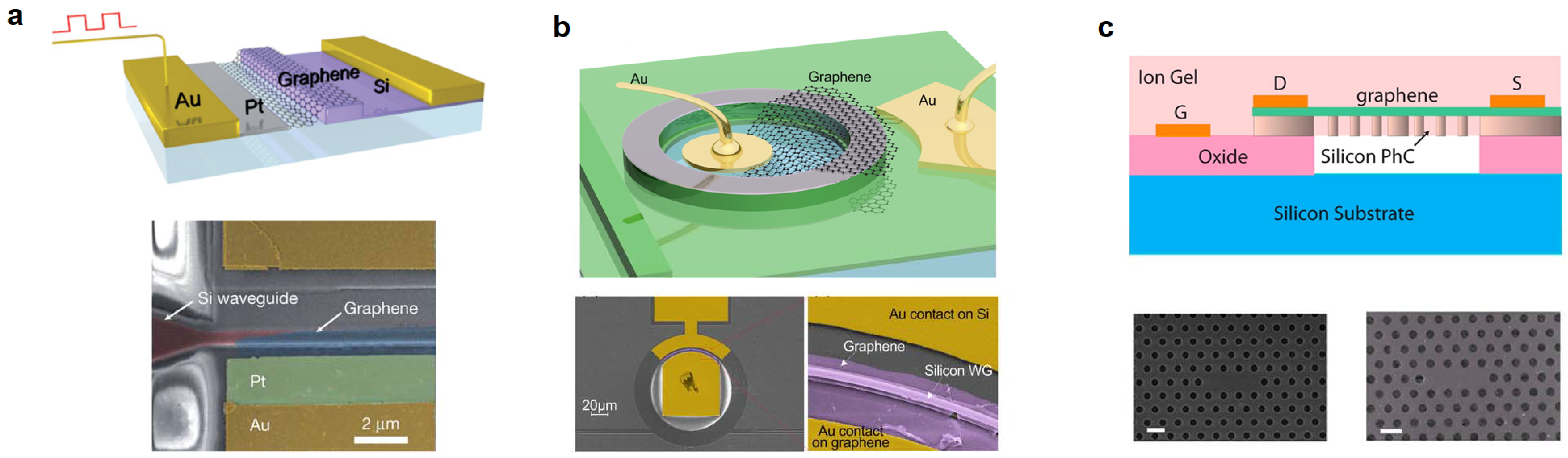
Photonic waveguides are another type of photonic structures that have been extensively studied to be combined with 2D optoelectronics to achieve a high-performance photodetector. Instead of top coupling, the incident light can be guided into the 2D photodetector by a waveguide through side coupling in order to achieve high photoresponsivity and fast response rate. In a recent report, a silicon waveguide-integrated BP photodetector has been demonstrated [103]. In comparison with graphene, the narrow bandgap nature allows BP to operate in the near-infrared band and, at the same time, preserve low dark current. As shown in Figure 4a, a silicon waveguide is planarized by SiO2 to accept an exfoliated BP thin layer. A graphene gate is then fabricated to control the doping of BP to optimize the device performance. The 11.5 nm thick BP device has obtained an intrinsic responsivity up to 135 mA/W, and an even higher responsivity up to 657 mA/W has been observed for 100 nm thick BP. Also, a high response speed ~3 GHz has been achieved while the dark current is limited to 220 nA. Graphene/silicon waveguide hybrid systems have also been demonstrated to present high performance. As shown in Figure 4b [104], a silicon waveguide is backfilled with SiO2 and then planarized. A 10 nm SiO2 layer is subsequently deposited on the planarized surface to electrically isolate the graphene layer from the underlying silicon structure. Two metal electrodes are placed asymmetrically to the waveguide to maximize the photocurrent collection. Without waveguide coupling, photocurrent signals are observed at the position of the waveguide at a level of 2.6 × 10⁻⁴ A/W under normal light incidence. However, when the optical waveguide mode couples to the graphene layer through the evanescent field to enhance the optical absorption, the detector achieves a photoresponsivity exceeding 0.1 A/W with a nearly uniform response between 1450 and 1590 nm. Moreover, response rates exceeding 20 GHz are observed under zero bias operation. A similar silicon waveguide-integrated graphene photodetector (Figure 4c) is reported by Pospischil et al. to present ultra-wideband response covering all optical communication band with a high speed ~18 GHz [105]. In order to improve the performance of the graphene/silicon waveguide hybrids, suspended membrane silicon waveguides have been combined with graphene to form heterojunctions as displayed in Figure 4d [106]. The waveguide enables absorption of the evanescent light that propagates parallel to the graphene sheet, resulting in a responsivity as high as 0.13 A/W at a 1.5 V bias for 2.75 μm light at room temperature. Additionally, to explain the photocurrent dependence on bias polarity, direct transitions in graphene are proposed when photon energy is larger than the two-fold energy difference between the Fermi level and Dirac point. On the other hand, when the photon energy goes below this energy difference, indirect transitions will become dominant.
3.2. Electro-Optic Modulator
The combination of photonic structures like waveguides, resonators or cavities with 2D materials enables the achievement of electro-optic modulator by electrostatically tuning 2D materials. A graphene-based broadband optical modulator is fabricated by placing a 250 nm-thick Si bus waveguide underneath a graphene sheet as illustrated in Figure 5a [107]. A 7 nm-thick Al2O3 spacer is placed between Si and graphene. The integration introduces several performance improvements: graphene provides strong light-matter interactions and broadband response covering telecommunication bandwidth, as well as mid- and far-infrared spectral regions. Furthermore, modulation of the guided light at frequencies over 1 GHz is demonstrated by electrically tuning the Fermi level of the graphene. Ring-shaped silicon microring resonators have also been reported to be combined with the graphene transistor as displayed in Figure 5b [108]. By tuning coverage lengths and electrostatic biases of graphene, a high extinction ratio of 12.8 dB is achieved. Photonic crystals are another extensively studied field to form various optical modulators such as resonators and cavities as the flow of light can be precisely molded. Photonic crystals are analogous to crystals where the unit structure is periodically duplicated [44,45,46]. When the periodicity in these structures approaches the wavelength of light, a photonic bandgap, in which the light propagation is forbidden, will appear. Under this circumstance, a pre-designed break in periodicity will introduce confinement of light. Photonic crystal/2D material hybrid systems are also reported in previous literatures [108,109,110,111,112,113]. Gan et al. have employed linear three-hole defect cavities in air-suspended 2D photonic crystals with graphene thin films transferred to the top [109]. The reflection attenuation and the increase of Raman signal intensity have demonstrated the local enhancement of light-matter interactions. Photonic crystals have also been reported to be integrated with 2D material phototransistors [110,111]. As shown in Figure 5c, optical cavities are fabricated by introducing point defects into 2D silicon photonic crystals [110]. The electrostatic properties of graphene are tuned by either source-drain biases or an ion-gel gate; as a result, a ~2 nm change in the cavity resonance line width and almost 400% (6 dB) modulation in resonance reflectivity are observed. Similar phenomena are reported for line defect photonic crystals [111].
In addition to the above discussions, the 2D optoelectronics also offer the possibilities to investigate the light modulation properties of photonic crystals considering the direct interaction between them [79]. Even photonic crystals have been extensively learned; their light manipulation manners can only be simulated by finite-difference time-domain (FDTD) simulations and detected by near-field scanning optical microscopy [114,115,116,117]. As described in Figure 4b, a graphene photodetector successfully detects a photocurrent strip on top of a silicon waveguide, which is attributed to the enhanced photocarrier density controlled by the waveguide. As a result, the photocurrent signals collected through the graphene photodetector directly visualize the light manipulation manners of the underneath silicon waveguide [104]. Recently, by directly contacting a featured silicon nanobeam with a BP photodetector, the spatially resolved photocurrent measurement is demonstrated to be an efficient approach to learn light-scattering properties of the silicon waveguide [79]. The direct contact between BP and the silicon waveguide enable photocarriers generated in the silicon to be injected into the BP. Since the density of photocarriers is related to the light distribution controlled by the waveguide, the spatial photocurrent signals detected by the BP photodetector reflect the light-scattering properties of the silicon waveguide, which shows strong dependence on both wavelength and polarization direction which are in good agreement with the prediction of FDTD.
4. Summary and Outlook
In this review, we summarize the current state-of-the-art in two-dimensional (2D) material-based optoelectronics, especially their integration with photonic structures. Several photocurrent-generation mechanisms, which have been reported in 2D material-based optoelectronics, are first introduced. Photonic structures, such as plasmonic nanostructures, photonic waveguides and crystals are subsequently described. For plasmonic nanostructures in 2D devices, metallic objects are placed on top of 2D materials as an ordered array with dimension and pitch in the order of the excitation wavelength. Those plasmonic nanostructures enable enhanced light absorption at certain wavelength ranges. Photonic waveguides are another type of nanoarchitectures to manipulate light flows. With the assistance of photonic crystals, those 2D material-based devices can achieve response with a high rate and efficiency. Besides, those combinations also make it possible to improve the performance of optical modulators by electrostatically manipulating 2D materials and to probe light-matter interactions of photonic crystals by scanning photocurrent measurements of 2D material-based optoelectronics. The study of photonic structure-integrated 2D material optoelectronics opens the avenues to engineer optoelectronics to meet versatile requirements for future applications.
Acknowledgments
This work was supported by the National Science Foundation (ECCS-1055852 and CBET-1264982).
Author Contributions
Tianjiao Wang and Yaqiong Xu wrote the paper.
Conflicts of Interest
The authors declare no conflict of interest.
References
- Geim, A.K.; Novoselov, K.S. The rise of graphene. Nat. Mater. 2007, 6, 183–191. [Google Scholar] [CrossRef] [PubMed]
- Schwierz, F. Graphene transistors. Nat. Nanotechnol. 2010, 5, 487–496. [Google Scholar] [CrossRef] [PubMed]
- Liao, L.; Lin, Y.-C.; Bao, M.; Cheng, R.; Bai, J.; Liu, Y.; Qu, Y.; Wang, K.L.; Huang, Y.; Duan, X. High-speed graphene transistors with a self-aligned nanowire gate. Nature 2010, 467, 305–308. [Google Scholar] [CrossRef] [PubMed]
- Wu, Y.; Lin, Y.-M.; Bol, A.A.; Jenkins, K.A.; Xia, F.; Farmer, D.B.; Zhu, Y.; Avouris, P. High-frequency, scaled graphene transistors on diamond-like carbon. Nature 2011, 472, 74–78. [Google Scholar] [CrossRef] [PubMed]
- Lin, Y.M.; Dimitrakopoulos, C.; Jenkins, K.A.; Farmer, D.B.; Chiu, H.Y.; Grill, A.; Avouris, P. 100-ghz transistors from wafer-scale epitaxial graphene. Science 2010, 327, 662. [Google Scholar] [CrossRef] [PubMed]
- Dean, C.R.; Young, A.F.; Meric, I.; Lee, C.; Wang, L.; Sorgenfrei, S.; Watanabe, K.; Taniguchi, T.; Kim, P.; Shepard, K.L.; et al. Boron nitride substrates for high-quality graphene electronics. Nat. Nanotechnol. 2010, 5, 722–726. [Google Scholar] [CrossRef]
- Britnell, L.; Gorbachev, R.V.; Geim, A.K.; Ponomarenko, L.A.; Mishchenko, A.; Greenaway, M.T.; Fromhold, T.M.; Novoselov, K.S.; Eaves, L. Resonant tunnelling and negative differential conductance in graphene transistors. Nat. Commun. 2013, 4, 1794. [Google Scholar] [CrossRef] [PubMed]
- Zhang, B.Y.; Liu, T.; Meng, B.; Li, X.; Liang, G.; Hu, X.; Wang, Q.J. Broadband high photoresponse from pure monolayer graphene photodetector. Nat. Commun. 2013, 4, 1811. [Google Scholar] [CrossRef] [PubMed]
- Xia, F.; Mueller, T.; Lin, Y.-m.; Valdes-Garcia, A.; Avouris, P. Ultrafast graphene photodetector. Nat. Nanotechnol. 2009, 4, 839–843. [Google Scholar] [CrossRef] [PubMed]
- Bonaccorso, F.; Sun, Z.; Hasan, T.; Ferrari, A.C. Graphene photonics and optoelectronics. Nat. Photonics 2010, 4, 611–622. [Google Scholar] [CrossRef]
- Radisavljevic, B.; Radenovic, A.; Brivio, J.; Giacometti, V.; Kis, A. Single-layer MoS2 transistors. Nat. Nanotechnol. 2011, 6, 147–150. [Google Scholar] [CrossRef] [PubMed]
- Larentis, S.; Fallahazad, B.; Tutuc, E. Field-effect transistors and intrinsic mobility in ultra-thin MoSe2 layers. Appl. Phys. Lett. 2012, 101, 223104. [Google Scholar] [CrossRef]
- Ramakrishna Matte, H.S.S.; Gomathi, A.; Manna, A.K.; Late, D.J.; Datta, R.; Pati, S.K.; Rao, C.N.R. MoS2 and WS2 analogues of graphene. Angew. Chem. 2010, 122, 4153–4156. [Google Scholar] [CrossRef]
- Fang, H.; Chuang, S.; Chang, T.C.; Takei, K.; Takahashi, T.; Javey, A. High-performance single layered WSe2 p-FETs with chemically doped contacts. Nano Lett. 2012, 12, 3788–3792. [Google Scholar] [CrossRef] [PubMed]
- Xia, F.; Wang, H.; Jia, Y. Rediscovering black phosphorus as an anisotropic layered material for optoelectronics and electronics. Nat. Commun. 2014, 5, 4458. [Google Scholar] [CrossRef] [PubMed]
- Wang, Q.H.; Kalantar-Zadeh, K.; Kis, A.; Coleman, J.N.; Strano, M.S. Electronics and optoelectronics of two-dimensional transition metal dichalcogenides. Nat. Nanotechnol. 2012, 7, 699–712. [Google Scholar] [CrossRef] [PubMed]
- Mak, K.F.; Shan, J. Photonics and optoelectronics of 2d semiconductor transition metal dichalcogenides. Nat. Photonics 2016, 10, 216–226. [Google Scholar] [CrossRef]
- Splendiani, A.; Sun, L.; Zhang, Y.; Li, T.; Kim, J.; Chim, C.-Y.; Galli, G.; Wang, F. Emerging photoluminescence in monolayer MoS2. Nano Lett. 2010, 10, 1271–1275. [Google Scholar] [CrossRef] [PubMed]
- Ross, J.S.; Klement, P.; Jones, A.M.; Ghimire, N.J.; Yan, J.; Mandrus, D.G.; Taniguchi, T.; Watanabe, K.; Kitamura, K.; Yao, W.; et al. Electrically tunable excitonic light-emitting diodes based on monolayer WSe2 p-n junctions. Nat. Nanotechnol. 2014, 9, 268–272. [Google Scholar] [CrossRef] [PubMed]
- Lee, C.; Yan, H.; Brus, L.E.; Heinz, T.F.; Hone, J.; Ryu, S. Anomalous lattice vibrations of single- and few-layer MoS2. ACS Nano 2010, 4, 2695–2700. [Google Scholar] [CrossRef] [PubMed]
- Lopez-Sanchez, O.; Lembke, D.; Kayci, M.; Radenovic, A.; Kis, A. Ultrasensitive photodetectors based on monolayer MoS2. Nat. Nano 2013, 8, 497–501. [Google Scholar] [CrossRef] [PubMed]
- Mak, K.F.; He, K.; Shan, J.; Heinz, T.F. Control of valley polarization in monolayer MoS2 by optical helicity. Nat. Nanotechnol. 2012, 7, 494–498. [Google Scholar] [CrossRef] [PubMed]
- Zeng, H.; Dai, J.; Yao, W.; Xiao, D.; Cui, X. Valley polarization in MoS2 monolayers by optical pumping. Nat. Nanotechnol. 2012, 7, 490–493. [Google Scholar] [CrossRef] [PubMed]
- Jones, A.M.; Yu, H.; Ghimire, N.J.; Wu, S.; Aivazian, G.; Ross, J.S.; Zhao, B.; Yan, J.; Mandrus, D.G.; Xiao, D.; et al. Optical generation of excitonic valley coherence in monolayer WSe2. Nat. Nanotechnol. 2013, 8, 634–638. [Google Scholar] [CrossRef] [PubMed]
- Chiritescu, C.; Cahill, D.G.; Nguyen, N.; Johnson, D.; Bodapati, A.; Keblinski, P.; Zschack, P. Ultralow thermal conductivity in disordered, layered WSe2 crystals. Science 2007, 315, 351–353. [Google Scholar] [CrossRef] [PubMed]
- Jariwala, D.; Sangwan, V.K.; Lauhon, L.J.; Marks, T.J.; Hersam, M.C. Emerging device applications for semiconducting two-dimensional transition metal dichalcogenides. ACS Nano 2014, 8, 1102–1120. [Google Scholar] [CrossRef] [PubMed]
- Li, T.; Galli, G. Electronic properties of MoS2 nanoparticles. J. Phys. Chem. C 2007, 111, 16192–16196. [Google Scholar] [CrossRef]
- Cheiwchanchamnangij, T.; Lambrecht, W.R.L. Quasiparticle band structure calculation of monolayer, bilayer, and bulk MoS2. Phys. Rev. B 2012, 85, 205302. [Google Scholar] [CrossRef]
- Mak, K.F.; Lee, C.; Hone, J.; Shan, J.; Heinz, T.F. Atomically thin MoS2: A new direct-gap semiconductor. Phys. Rev. Lett. 2010, 105, 136805. [Google Scholar] [CrossRef] [PubMed]
- Xiao, D.; Liu, G.-B.; Feng, W.; Xu, X.; Yao, W. Coupled spin and valley physics in monolayers of MoS2 and other group-VI dichalcogenides. Phys. Rev. Lett. 2012, 108, 196802. [Google Scholar] [CrossRef] [PubMed]
- Cao, T.; Wang, G.; Han, W.; Ye, H.; Zhu, C.; Shi, J.; Niu, Q.; Tan, P.; Wang, E.; Liu, B.; et al. Valley-selective circular dichroism of monolayer molybdenum disulphide. Nat. Commun. 2012, 3, 887. [Google Scholar] [CrossRef] [PubMed]
- Mak, K.F.; McGill, K.L.; Park, J.; McEuen, P.L. The valley hall effect in MoS2 transistors. Science 2014, 344, 1489–1492. [Google Scholar] [CrossRef] [PubMed]
- Shi, Y.; Hamsen, C.; Jia, X.; Kim, K.K.; Reina, A.; Hofmann, M.; Hsu, A.L.; Zhang, K.; Li, H.; Juang, Z.-Y.; et al. Synthesis of few-layer hexagonal boron nitride thin film by chemical vapor deposition. Nano Lett. 2010, 10, 4134–4139. [Google Scholar] [CrossRef] [PubMed]
- Li, L.; Yu, Y.; Ye, G.J.; Ge, Q.; Ou, X.; Wu, H.; Feng, D.; Chen, X.H.; Zhang, Y. Black phosphorus field-effect transistors. Nat. Nanotechnol. 2014, 9, 372–377. [Google Scholar] [CrossRef] [PubMed]
- Qiao, J.; Kong, X.; Hu, Z.-X.; Yang, F.; Ji, W. High-mobility transport anisotropy and linear dichroism in few-layer black phosphorus. Nat. Commun. 2014, 5, 4475. [Google Scholar] [CrossRef] [PubMed]
- Tran, V.; Soklaski, R.; Liang, Y.; Yang, L. Layer-controlled band gap and anisotropic excitons in few-layer black phosphorus. Phys. Rev. B 2014, 89, 235319. [Google Scholar] [CrossRef]
- Koenig, S.P.; Doganov, R.A.; Schmidt, H.; Castro Neto, A.H.; Özyilmaz, B. Electric field effect in ultrathin black phosphorus. Appl. Phys. Lett. 2014, 104, 103106. [Google Scholar] [CrossRef]
- Andres, C.-G.; Leonardo, V.; Elsa, P.; Joshua, O.I.; Narasimha-Acharya, K.L.; Sofya, I.B.; Dirk, J.G.; Michele, B.; Gary, A.S.; Alvarez, J.V.; et al. Isolation and characterization of few-layer black phosphorus. 2D Mater. 2014, 1, 025001. [Google Scholar]
- Buscema, M.; Groenendijk, D.J.; Blanter, S.I.; Steele, G.A.; van der Zant, H.S.J.; Castellanos-Gomez, A. Fast and broadband photoresponse of few-layer black phosphorus field-effect transistors. Nano Lett. 2014, 14, 3347–3352. [Google Scholar] [CrossRef] [PubMed]
- Mannix, A.J.; Zhou, X.-F.; Kiraly, B.; Wood, J.D.; Alducin, D.; Myers, B.D.; Liu, X.; Fisher, B.L.; Santiago, U.; Guest, J.R.; et al. Synthesis of borophenes: Anisotropic, two-dimensional boron polymorphs. Science 2015, 350, 1513–1516. [Google Scholar] [CrossRef] [PubMed]
- Osada, M.; Sasaki, T. Two-dimensional dielectric nanosheets: Novel nanoelectronics from nanocrystal building blocks. Adv. Mater. 2012, 24, 210–228. [Google Scholar] [CrossRef] [PubMed]
- Nair, R.R.; Blake, P.; Grigorenko, A.N.; Novoselov, K.S.; Booth, T.J.; Stauber, T.; Peres, N.M.R.; Geim, A.K. Fine structure constant defines visual transparency of graphene. Science 2008, 320, 1308. [Google Scholar] [CrossRef] [PubMed]
- Eda, G.; Maier, S.A. Two-dimensional crystals: Managing light for optoelectronics. ACS Nano 2013, 7, 5660–5665. [Google Scholar] [CrossRef] [PubMed]
- Geim, A.K.; Grigorieva, I.V. Van der waals heterostructures. Nature 2013, 499, 419–425. [Google Scholar] [CrossRef] [PubMed]
- Koenderink, A.F.; Alù, A.; Polman, A. Nanophotonics: Shrinking light-based technology. Science 2015, 348, 516–521. [Google Scholar] [CrossRef] [PubMed]
- Bao, Q.; Loh, K.P. Graphene photonics, plasmonics, and broadband optoelectronic devices. ACS Nano 2012, 6, 3677–3694. [Google Scholar] [CrossRef] [PubMed]
- Grigorenko, A.N.; Polini, M.; Novoselov, K.S. Graphene plasmonics. Nat. Photonics 2012, 6, 749–758. [Google Scholar] [CrossRef]
- Brar, V.W.; Jang, M.S.; Sherrott, M.; Lopez, J.J.; Atwater, H.A. Highly confined tunable mid-infrared plasmonics in graphene nanoresonators. Nano Lett. 2013, 13, 2541–2547. [Google Scholar] [CrossRef] [PubMed]
- Brar, V.W.; Jang, M.S.; Sherrott, M.; Kim, S.; Lopez, J.J.; Kim, L.B.; Choi, M.; Atwater, H. Hybrid surface-phonon-plasmon polariton modes in graphene/monolayer h-bn heterostructures. Nano Lett. 2014, 14, 3876–3880. [Google Scholar] [CrossRef] [PubMed]
- Jang, M.S.; Brar, V.W.; Sherrott, M.C.; Lopez, J.J.; Kim, L.; Kim, S.; Choi, M.; Atwater, H.A. Tunable large resonant absorption in a midinfrared graphene salisbury screen. Phys. Rev. B 2014, 90, 165409. [Google Scholar] [CrossRef]
- Brar, V.W.; Sherrott, M.C.; Jang, M.S.; Kim, S.; Kim, L.; Choi, M.; Sweatlock, L.A.; Atwater, H.A. Electronic modulation of infrared radiation in graphene plasmonic resonators. Nat. Commun. 2015, 6, 7032. [Google Scholar] [CrossRef] [PubMed]
- Jariwala, D.; Davoyan, A.R.; Tagliabue, G.; Sherrott, M.C.; Wong, J.; Atwater, H.A. Near-unity absorption in van der waals semiconductors for ultrathin optoelectronics. Nano Lett. 2016, 16, 5482–5487. [Google Scholar] [CrossRef] [PubMed]
- Xia, F.; Wang, H.; Xiao, D.; Dubey, M.; Ramasubramaniam, A. Two-dimensional material nanophotonics. Nat. Photonics 2014, 8, 899–907. [Google Scholar] [CrossRef]
- Buscema, M.; Island, J.O.; Groenendijk, D.J.; Blanter, S.I.; Steele, G.A.; van der Zant, H.S.J.; Castellanos-Gomez, A. Photocurrent generation with two-dimensional van der waals semiconductors. Chem. Soc. Rev. 2015, 44, 3691–3718. [Google Scholar] [CrossRef] [PubMed]
- Bhimanapati, G.R.; Lin, Z.; Meunier, V.; Jung, Y.; Cha, J.; Das, S.; Xiao, D.; Son, Y.; Strano, M.S.; Cooper, V.R.; et al. Recent advances in two-dimensional materials beyond graphene. ACS Nano 2015, 9, 11509–11539. [Google Scholar] [CrossRef] [PubMed]
- Butler, S.Z.; Hollen, S.M.; Cao, L.; Cui, Y.; Gupta, J.A.; Gutiérrez, H.R.; Heinz, T.F.; Hong, S.S.; Huang, J.; Ismach, A.F.; et al. Progress, challenges, and opportunities in two-dimensional materials beyond graphene. ACS Nano 2013, 7, 2898–2926. [Google Scholar] [CrossRef] [PubMed]
- Xu, M.; Liang, T.; Shi, M.; Chen, H. Graphene-like two-dimensional materials. Chem. Rev. 2013, 113, 3766–3798. [Google Scholar] [CrossRef] [PubMed]
- Howell, S.L.; Jariwala, D.; Wu, C.-C.; Chen, K.-S.; Sangwan, V.K.; Kang, J.; Marks, T.J.; Hersam, M.C.; Lauhon, L.J. Investigation of band-offsets at monolayer–multilayer MoS2 junctions by scanning photocurrent microscopy. Nano Lett. 2015, 15, 2278–2284. [Google Scholar] [CrossRef] [PubMed]
- Wu, C.-C.; Jariwala, D.; Sangwan, V.K.; Marks, T.J.; Hersam, M.C.; Lauhon, L.J. Elucidating the photoresponse of ultrathin MoS2 field-effect transistors by scanning photocurrent microscopy. J. Phys. Chem. Lett. 2013, 4, 2508–2513. [Google Scholar] [CrossRef]
- Furchi, M.M.; Polyushkin, D.K.; Pospischil, A.; Mueller, T. Mechanisms of photoconductivity in atomically thin MoS2. Nano Lett. 2014, 14, 6165–6170. [Google Scholar] [CrossRef] [PubMed]
- Park, J.; Ahn, Y.H.; Ruiz-Vargas, C. Imaging of photocurrent generation and collection in single-layer graphene. Nano Lett. 2009, 9, 1742–1746. [Google Scholar] [CrossRef] [PubMed]
- Xia, F.; Mueller, T.; Golizadeh-Mojarad, R.; Freitag, M.; Lin, Y.-M.; Tsang, J.; Perebeinos, V.; Avouris, P. Photocurrent imaging and efficient photon detection in a graphene transistor. Nano Lett. 2009, 9, 1039–1044. [Google Scholar] [CrossRef] [PubMed]
- Yin, Z.; Li, H.; Li, H.; Jiang, L.; Shi, Y.; Sun, Y.; Lu, G.; Zhang, Q.; Chen, X.; Zhang, H. Single-layer MoS2 phototransistors. ACS Nano 2012, 6, 74–80. [Google Scholar] [CrossRef] [PubMed]
- Nolas, G.S.; Sharp, J.; Goldsmid, J. Thermoelectrics: Basic Principles and New Materials Developments; Springer Science & Business Media: New York, NY, USA, 2013; Volume 45. [Google Scholar]
- Cutler, M.; Mott, N.F. Observation of anderson localization in an electron gas. Phys. Rev. 1969, 181, 1336–1340. [Google Scholar] [CrossRef]
- Xu, X.; Gabor, N.M.; Alden, J.S.; van der Zande, A.M.; McEuen, P.L. Photo-thermoelectric effect at a graphene interface junction. Nano Lett. 2010, 10, 562–566. [Google Scholar] [CrossRef] [PubMed]
- Seol, J.H.; Jo, I.; Moore, A.L.; Lindsay, L.; Aitken, Z.H.; Pettes, M.T.; Li, X.; Yao, Z.; Huang, R.; Broido, D.; et al. Two-dimensional phonon transport in supported graphene. Science 2010, 328, 213–216. [Google Scholar] [CrossRef] [PubMed]
- Grosse, K.L.; Bae, M.-H.; Lian, F.; Pop, E.; King, W.P. Nanoscale joule heating, peltier cooling and current crowding at graphene-metal contacts. Nat. Nano 2011, 6, 287–290. [Google Scholar] [CrossRef] [PubMed]
- Wang, Z.; Xie, R.; Bui, C.T.; Liu, D.; Ni, X.; Li, B.; Thong, J.T.L. Thermal transport in suspended and supported few-layer graphene. Nano Lett. 2011, 11, 113–118. [Google Scholar] [CrossRef] [PubMed]
- Wu, J.; Schmidt, H.; Amara, K.K.; Xu, X.; Eda, G.; Özyilmaz, B. Large thermoelectricity via variable range hopping in chemical vapor deposition grown single-layer MoS2. Nano Lett. 2014, 14, 2730–2734. [Google Scholar] [CrossRef] [PubMed]
- Buscema, M.; Barkelid, M.; Zwiller, V.; van der Zant, H.S.J.; Steele, G.A.; Castellanos-Gomez, A. Large and tunable photothermoelectric effect in single-layer MoS2. Nano Lett. 2013, 13, 358–363. [Google Scholar] [CrossRef] [PubMed]
- Low, T.; Engel, M.; Steiner, M.; Avouris, P. Origin of photoresponse in black phosphorus phototransistors. Phys. Rev. B 2014, 90, 081408. [Google Scholar] [CrossRef]
- Flores, E.; Ares, J.R.; Castellanos-Gomez, A.; Barawi, M.; Ferrer, I.J.; Sánchez, C. Thermoelectric power of bulk black-phosphorus. Appl. Phys. Lett. 2015, 106, 022102. [Google Scholar] [CrossRef]
- Engel, M.; Steiner, M.; Avouris, P. Black phosphorus photodetector for multispectral, high-resolution imaging. Nano Lett. 2014, 14, 6414–6417. [Google Scholar] [CrossRef] [PubMed]
- Tsen, A.W.; DonevLuke, A.K.; Kurt, H.; Herman, L.H.; Park, J. Imaging the electrical conductance of individual carbon nanotubes with photothermal current microscopy. Nat. Nano 2009, 4, 108–113. [Google Scholar] [CrossRef] [PubMed]
- Gabor, N.M.; Song, J.C.W.; Ma, Q.; Nair, N.L.; Taychatanapat, T.; Watanabe, K.; Taniguchi, T.; Levitov, L.S.; Jarillo-Herrero, P. Hot carrier–assisted intrinsic photoresponse in graphene. Science 2011, 334, 648–652. [Google Scholar] [CrossRef] [PubMed]
- Freitag, M.; Low, T.; Xia, F.; Avouris, P. Photoconductivity of biased graphene. Nat. Photonics 2013, 7, 53–59. [Google Scholar] [CrossRef]
- Hong, T.; Chamlagain, B.; Hu, S.; Weiss, S.M.; Zhou, Z.; Xu, Y.-Q. Plasmonic hot electron induced photocurrent response at MoS2–metal junctions. ACS Nano 2015, 9, 5357–5363. [Google Scholar] [CrossRef] [PubMed]
- Wang, T.; Hu, S.; Chamlagain, B.; Hong, T.; Zhou, Z.; Weiss, S.M.; Xu, Y.-Q. Visualizing light scattering in silicon waveguides with black-phosphorus photodetectors. Adv. Mater. 2016, 28, 7162–7166. [Google Scholar] [CrossRef] [PubMed]
- Néstor, P.-L.; Zhong, L.; Nihar, R.P.; Agustín, I.-R.; Ana Laura, E.; Amber, M.; Jun, L.; Pulickel, M.A.; Humberto, T.; Luis, B.; et al. Cvd-grown monolayered MoS2 as an effective photosensor operating at low-voltage. 2D Mater. 2014, 1, 011004. [Google Scholar]
- Mueller, T.; Xia, F.; Avouris, P. Graphene photodetectors for high-speed optical communications. Nat. Photonics 2010, 4, 297–301. [Google Scholar] [CrossRef]
- Zhang, W.; Chiu, M.-H.; Chen, C.-H.; Chen, W.; Li, L.-J.; Wee, A.T.S. Role of metal contacts in high-performance phototransistors based on WSe2 monolayers. ACS Nano 2014, 8, 8653–8661. [Google Scholar] [CrossRef] [PubMed]
- Hong, T.; Chamlagain, B.; Lin, W.; Chuang, H.-J.; Pan, M.; Zhou, Z.; Xu, Y.-Q. Polarized photocurrent response in black phosphorus field-effect transistors. Nanoscale 2014, 6, 8978–8983. [Google Scholar] [CrossRef] [PubMed]
- Wang, H.; Liu, F.; Fu, W.; Fang, Z.; Zhou, W.; Liu, Z. Two-dimensional heterostructures: Fabrication, characterization, and application. Nanoscale 2014, 6, 12250–12272. [Google Scholar] [CrossRef] [PubMed]
- Withers, F.; Del Pozo-Zamudio, O.; Mishchenko, A.; Rooney, A.P.; Gholinia, A.; Watanabe, K.; Taniguchi, T.; Haigh, S.J.; Geim, A.K.; Tartakovskii, A.I.; et al. Light-emitting diodes by band-structure engineering in van der waals heterostructures. Nat. Mater. 2015, 14, 301–306. [Google Scholar] [CrossRef] [PubMed]
- Niu, T.; Li, A. From two-dimensional materials to heterostructures. Prog. Surface Sci. 2015, 90, 21–45. [Google Scholar] [CrossRef]
- Jariwala, D.; Howell, S.L.; Chen, K.-S.; Kang, J.; Sangwan, V.K.; Filippone, S.A.; Turrisi, R.; Marks, T.J.; Lauhon, L.J.; Hersam, M.C. Hybrid, gate-tunable, van der waals p–n heterojunctions from pentacene and MoS2. Nano Lett. 2016, 16, 497–503. [Google Scholar] [CrossRef] [PubMed]
- Jariwala, D.; Sangwan, V.K.; Wu, C.-C.; Prabhumirashi, P.L.; Geier, M.L.; Marks, T.J.; Lauhon, L.J.; Hersam, M.C. Gate-tunable carbon nanotube–MoS2 heterojunction p-n diode. Proc. Natl. Acad. Sci. USA 2013, 110, 18076–18080. [Google Scholar] [CrossRef] [PubMed]
- Jariwala, D.; Marks, T.J.; Hersam, M.C. Mixed-dimensional van der waals heterostructures. Nat. Mater. 2016. [Google Scholar] [CrossRef] [PubMed]
- Deng, Y.; Luo, Z.; Conrad, N.J.; Liu, H.; Gong, Y.; Najmaei, S.; Ajayan, P.M.; Lou, J.; Xu, X.; Ye, P.D. Black phosphorus–monolayer MoS2 van der waals heterojunction p–n diode. ACS Nano 2014, 8, 8292–8299. [Google Scholar] [CrossRef] [PubMed]
- Hong, T.; Chamlagain, B.; Wang, T.; Chuang, H.-J.; Zhou, Z.; Xu, Y.-Q. Anisotropic photocurrent response at black phosphorus-MoS2 p-n heterojunctions. Nanoscale 2015, 7, 18537–18541. [Google Scholar] [CrossRef] [PubMed]
- Wang, L.; Meric, I.; Huang, P.Y.; Gao, Q.; Gao, Y.; Tran, H.; Taniguchi, T.; Watanabe, K.; Campos, L.M.; Muller, D.A.; et al. One-dimensional electrical contact to a two-dimensional material. Science 2013, 342, 614–617. [Google Scholar] [CrossRef] [PubMed]
- Liu, W.; Lee, B.; Naylor, C.H.; Ee, H.-S.; Park, J.; Johnson, A.T.C.; Agarwal, R. Strong exciton–plasmon coupling in MoS2 coupled with plasmonic lattice. Nano Lett. 2016, 16, 1262–1269. [Google Scholar] [CrossRef] [PubMed]
- Lee, B.; Park, J.; Han, G.H.; Ee, H.-S.; Naylor, C.H.; Liu, W.; Johnson, A.T.C.; Agarwal, R. Fano resonance and spectrally modified photoluminescence enhancement in monolayer MoS2 integrated with plasmonic nanoantenna array. Nano Lett. 2015, 15, 3646–3653. [Google Scholar] [CrossRef] [PubMed]
- Sobhani, A.; Lauchner, A.; Najmaei, S.; Ayala-Orozco, C.; Wen, F.; Lou, J.; Halas, N.J. Enhancing the photocurrent and photoluminescence of single crystal monolayer MoS2 with resonant plasmonic nanoshells. Appl. Phys. Lett. 2014, 104, 031112. [Google Scholar] [CrossRef]
- Butun, S.; Tongay, S.; Aydin, K. Enhanced light emission from large-area monolayer MoS2 using plasmonic nanodisc arrays. Nano Lett. 2015, 15, 2700–2704. [Google Scholar] [CrossRef] [PubMed]
- Kim, S.; Jang, M.S.; Brar, V.W.; Tolstova, Y.; Mauser, K.W.; Atwater, H.A. Electronically tunable extraordinary optical transmission in graphene plasmonic ribbons coupled to subwavelength metallic slit arrays. Nat. Commun. 2016, 7, 12323. [Google Scholar] [CrossRef] [PubMed]
- Najmaei, S.; Mlayah, A.; Arbouet, A.; Girard, C.; Léotin, J.; Lou, J. Plasmonic pumping of excitonic photoluminescence in hybrid MoS2–au nanostructures. ACS Nano 2014, 8, 12682–12689. [Google Scholar] [CrossRef] [PubMed]
- Miao, J.; Hu, W.; Jing, Y.; Luo, W.; Liao, L.; Pan, A.; Wu, S.; Cheng, J.; Chen, X.; Lu, W. Surface plasmon-enhanced photodetection in few layer MoS2 phototransistors with au nanostructure arrays. Small 2015, 11, 2392–2398. [Google Scholar] [CrossRef] [PubMed]
- Wang, W.; Klots, A.; Prasai, D.; Yang, Y.; Bolotin, K.I.; Valentine, J. Hot electron-based near-infrared photodetection using bilayer MoS2. Nano Lett. 2015, 15, 7440–7444. [Google Scholar] [CrossRef] [PubMed]
- Liu, Y.; Cheng, R.; Liao, L.; Zhou, H.; Bai, J.; Liu, G.; Liu, L.; Huang, Y.; Duan, X. Plasmon resonance enhanced multicolour photodetection by graphene. Nat. Commun. 2011, 2, 579. [Google Scholar] [CrossRef] [PubMed]
- Echtermeyer, T.J.; Britnell, L.; Jasnos, P.K.; Lombardo, A.; Gorbachev, R.V.; Grigorenko, A.N.; Geim, A.K.; Ferrari, A.C.; Novoselov, K.S. Strong plasmonic enhancement of photovoltage in graphene. Nat. Commun. 2011, 2, 458. [Google Scholar] [CrossRef] [PubMed]
- Youngblood, N.; Chen, C.; Koester, S.J.; Li, M. Waveguide-integrated black phosphorus photodetector with high responsivity and low dark current. Nat. Photonics 2015, 9, 247–252. [Google Scholar] [CrossRef]
- Gan, X.; Shiue, R.-J.; Gao, Y.; Meric, I.; Heinz, T.F.; Shepard, K.; Hone, J.; Assefa, S.; Englund, D. Chip-integrated ultrafast graphene photodetector with high responsivity. Nat. Photonics 2013, 7, 883–887. [Google Scholar] [CrossRef]
- Pospischil, A.; Humer, M.; Furchi, M.M.; Bachmann, D.; Guider, R.; Fromherz, T.; Mueller, T. Cmos-compatible graphene photodetector covering all optical communication bands. Nat. Photonics 2013, 7, 892–896. [Google Scholar] [CrossRef]
- Wang, X.; Cheng, Z.; Xu, K.; Tsang, H.K.; Xu, J.-B. High-responsivity graphene/silicon-heterostructure waveguide photodetectors. Nat. Photonics 2013, 7, 888–891. [Google Scholar] [CrossRef]
- Liu, M.; Yin, X.; Ulin-Avila, E.; Geng, B.; Zentgraf, T.; Ju, L.; Wang, F.; Zhang, X. A graphene-based broadband optical modulator. Nature 2011, 474, 64–67. [Google Scholar] [CrossRef] [PubMed]
- Ding, Y.; Zhu, X.; Xiao, S.; Hu, H.; Frandsen, L.H.; Mortensen, N.A.; Yvind, K. Effective electro-optical modulation with high extinction ratio by a graphene-silicon microring resonator. Nano Lett. 2015, 15, 4393–4400. [Google Scholar] [CrossRef] [PubMed]
- Gan, X.; Mak, K.F.; Gao, Y.; You, Y.; Hatami, F.; Hone, J.; Heinz, T.F.; Englund, D. Strong enhancement of light-matter interaction in graphene coupled to a photonic crystal nanocavity. Nano Lett. 2012, 12, 5626–5631. [Google Scholar] [CrossRef] [PubMed]
- Majumdar, A.; Kim, J.; Vuckovic, J.; Wang, F. Electrical control of silicon photonic crystal cavity by graphene. Nano Lett. 2013, 13, 515–518. [Google Scholar] [CrossRef] [PubMed]
- Gan, X.; Shiue, R.-J.; Gao, Y.; Mak, K.F.; Yao, X.; Li, L.; Szep, A.; Walker, D.; Hone, J.; Heinz, T.F.; et al. High-contrast electrooptic modulation of a photonic crystal nanocavity by electrical gating of graphene. Nano Lett. 2013, 13, 691–696. [Google Scholar] [CrossRef] [PubMed]
- Wu, S.; Buckley, S.; Schaibley, J.R.; Feng, L.; Yan, J.; Mandrus, D.G.; Hatami, F.; Yao, W.; Vuckovic, J.; Majumdar, A.; et al. Monolayer semiconductor nanocavity lasers with ultralow thresholds. Nature 2015, 520, 69–72. [Google Scholar] [CrossRef] [PubMed] [Green Version]
- Majumdar, A.; Dodson, C.M.; Fryett, T.K.; Zhan, A.; Buckley, S.; Gerace, D. Hybrid 2D material nanophotonics: A scalable platform for low-power nonlinear and quantum optics. ACS Photonics 2015, 2, 1160–1166. [Google Scholar] [CrossRef]
- Kunz, K.S.; Luebbers, R.J. The finite difference time domain method for electromagnetics; CRC press: Boca Raton, FL, USA, 1993. [Google Scholar]
- Hu, S.; Weiss, S.M. Design of photonic crystal cavities for extreme light concentration. ACS Photonics 2016, 3, 1647–1653. [Google Scholar] [CrossRef]
- Ee, H.-S.; Kang, J.-H.; Brongersma, M.L.; Seo, M.-K. Shape-dependent light scattering properties of subwavelength silicon nanoblocks. Nano Lett. 2015, 15, 1759–1765. [Google Scholar] [CrossRef] [PubMed]
- Dunn, R.C. Near-field scanning optical microscopy. Chem. Rev. 1999, 99, 2891–2928. [Google Scholar] [CrossRef] [PubMed]
Figure 1.
Schematic representation of photocurrent-generation mechanisms in semiconducting 2D materials. M and S indicate metal electrode contacts and 2D semiconductor channels, respectively. (a) Photon-excited electron-hole pairs (EHPs) separated by internal electric fields at metal-semiconductor Schottky barriers. Red shaded areas indicate an elevated temperature ΔT induced by laser heating, leading to (b) a voltage difference ΔVPTE or (c) overall conductance change ΔG across the channel; (d) Carriers are injected from metal electrodes into a 2D material channel.

Figure 2.
Photocurrent generation in 2D materials. (a) Optical image of monolayer MoS2-based field effect transistor (top) and band diagrams under different illumination and bias conditions (bottom), reproduced with permission from [63], ACS, 2012; (b) 3D schematic of a dual-gated graphene phototransistor (top) and six-fold photovoltage pattern occurs while the top and bottom gate biases change (bottom), reproduced with permission from [76], AAAS, 2011; (c) Reflection image of a strongly doped graphene phototransistor (top) and bolometric photocurrent observed to exhibit opposite polarities to applied biases (bottom), reproduced with permission from [77], Nature Publishing Group, 2012; (d) A four-electrode MoS2 phototransistor (top), photocurrent signals that show different anisotropic behaviors with photo energy above/below the MoS2 bandgap (middle), and hot electron injection that is proposed to be dominant when the photon energy is below the band gap of MoS2 (bottom), reproduced with permission from [78], ACS, 2015.

Figure 3.
Plasmonic nanostructure-integrated 2D material photodetectors. (a) Schematic diagram (left-top) and optical image (right-top) of a device, in which MoS2 is in direct contact with Au on the left side, while a 10 nm thick Al2O3 film is placed between MoS2 and Au on the right side. Photocurrent measured from the left (upper panel) and the right (lower panel) subdevice (bottom), reproduced with permission from [100], ACS, 2015; (b) 3D schematic of a graphene transistor underneath gold nanoparticles (left) and photoresponse enhancement as a function of wavelength (right), reproduced with permission from [101], Nature Publishing Group, 2011; (c) Optical image of graphene phototransistors with different plasmonic nanostructures (left) and photovoltages at various gate biases (right), reproduced with permission from [102], Nature Publishing Group, 2011.
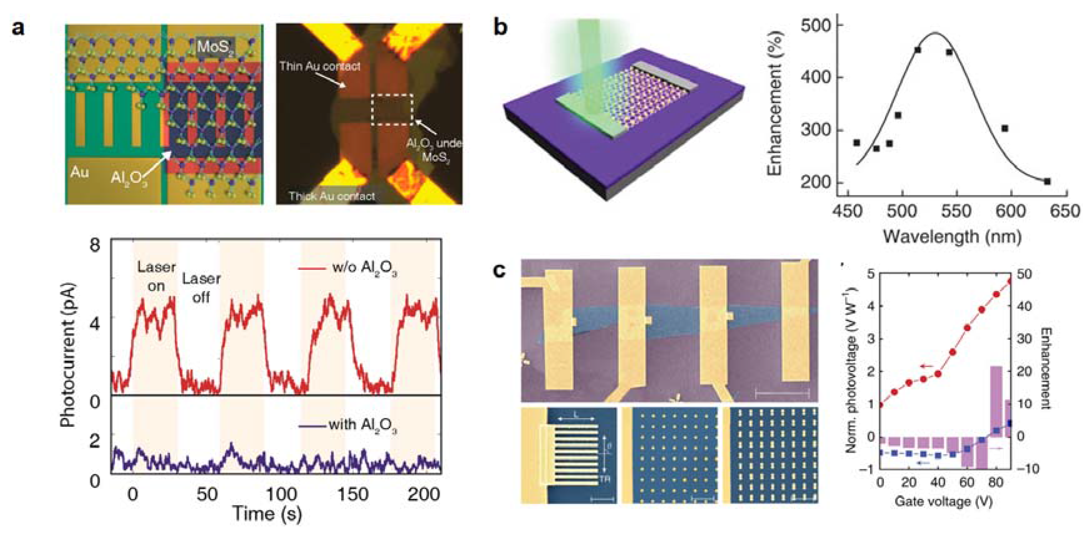
Figure 4.
Waveguide-integrated 2D material photodetectors (a) 3D illustration of a silicon waveguide-integrated BP photodetector, featuring a few-layer graphene top-gate (top) and broadband frequency response of the BP photodetector with low or high doping (bottom), reproduced with permission from [103], Nature Publishing Group, 2013; (b) Schematic of a silicon waveguide-integrated graphene photodetector (top) and band diagram that shows photocurrent-generation mechanisms (bottom), reproduced with permission from [104], Nature Publishing Group, 2013; (c) Scanning electron micrograph (SEM) image of a silicon nanobeam-integrated graphene photodetector (top) and band diagram along the lateral direction (bottom), reproduced with permission from [105], Nature Publishing Group, 2013; (d) 3D schematic of a graphene-silicon heterostructure waveguide photodetector (top) and SEM image (bottom), reproduced with permission from [106], Nature Publishing Group, 2013.
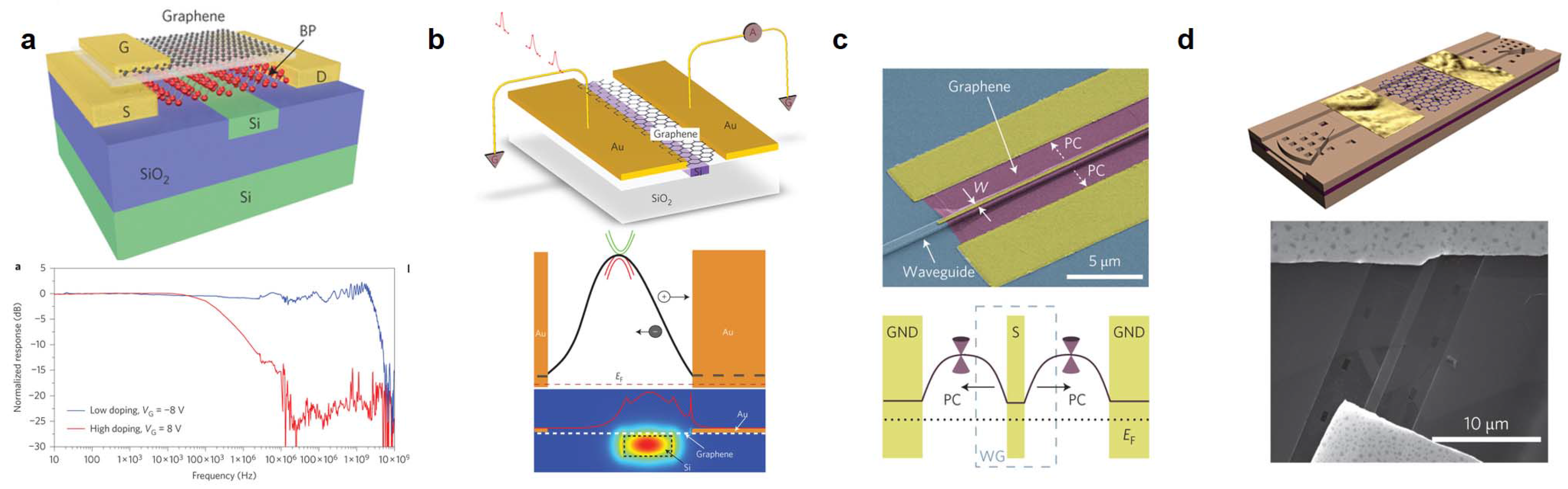
Figure 5.
A 2D electronics-integrated optical modulator. (a) Schematic of a high-bandwidth graphene-integrated silicon waveguide modulator (top) and top view of the structure (bottom), reproduced with permission from [107], Nature Publishing Group, 2011; (b) Schematic of a graphene-silicon microring device (top), false-color SEM image of the fabricated device (left bottom), and a zoom-in SEM image of the bended silicon waveguide covered by graphene (right bottom), reproduced with permission from [108], ACS, 2015; (c) Schematic of the photonic crystal cavity–graphene device. SEM image of the fabricated cavities without (left bottom), and with graphene (right bottom), reproduced with permission from [110], ACS, 2013.


| Application | Photonic Structures | 2D Material | Performance | Ref. | |
|---|---|---|---|---|---|
| Photodetector | Plasmonic Nanostructure | Au Particle | MoS2 | Photoresponsivity: 200%–300% enhancement | [99] |
| Au Antenna Array | MoS2 | Photoresponsivity: 5.2 A/W Photogain: 105 | [100] | ||
| Au Particle | Graphene | Photoresponsivity: 1500% enhancement | [101] | ||
| Ti/Au nanostructures | Graphene | Photoresponsivity: 2000% enhancement | [102] | ||
| Waveguide | Si Waveguide | BP | Photoresponsivity: 657 mA/W response rate: ~3 GHz | [103] | |
| Si Waveguide | Graphene | Photoresponsivity: 0.1 A/W response rate: ~20 GHz | [104] | ||
| Si Waveguide | Graphene | Response wavelength range: all optical communication band response rate: ~18 GHz | [105] | ||
| Suspended Waveguide | Graphene | Photoresponsivity: 0.13 A/W | [106] | ||
| Modulator | Waveguide | Si Waveguide | Graphene | Modulation Depth: 3 dB operation speed: over 1 GHz bandwidth: 1.35–1.6 μm | [107] |
| Si Microring Resonator | Graphene | Modulation Depth: 12.5 dB | [108] | ||
| Photonic Crystal | 2D Photonic Crystal Nanocavity | Graphene | Modulation Depth: 6 dB | [110] | |
© 2016 by the authors; licensee MDPI, Basel, Switzerland. This article is an open access article distributed under the terms and conditions of the Creative Commons Attribution (CC-BY) license (http://creativecommons.org/licenses/by/4.0/).
Share and Cite
MDPI and ACS Style
Wang, T.; Xu, Y.-Q. Photonic Structure-Integrated Two-Dimensional Material Optoelectronics. Electronics 2016, 5, 93. https://doi.org/10.3390/electronics5040093
AMA Style
Wang T, Xu Y-Q. Photonic Structure-Integrated Two-Dimensional Material Optoelectronics. Electronics. 2016; 5(4):93. https://doi.org/10.3390/electronics5040093
Chicago/Turabian StyleWang, Tianjiao, and Ya-Qiong Xu. 2016. "Photonic Structure-Integrated Two-Dimensional Material Optoelectronics" Electronics 5, no. 4: 93. https://doi.org/10.3390/electronics5040093
Note that from the first issue of 2016, this journal uses article numbers instead of page numbers. See further details here.