Review

Progress towards Spin-Based Light Emission in Group IV Semiconductors

LNESS and Dipartimento di Scienza dei Materiali, Università degli Studi di Milano-Bicocca, via Cozzi 55, I-20125 Milano, Italy
*
Authors to whom correspondence should be addressed.
Electronics 2017, 6(1), 19; https://doi.org/10.3390/electronics6010019
Submission received: 21 December 2016 / Revised: 27 January 2017 / Accepted: 20 February 2017 / Published: 7 March 2017
(This article belongs to the Special Issue Spin Optoelectronics)

Abstract

:
Spin-optoelectronics is an emerging technology in which novel and advanced functionalities are enabled by the synergetic integration of magnetic, optical and electronic properties onto semiconductor-based devices. This article reviews the possible implementation and convergence of spintronics and photonics concepts on group IV semiconductors: the core materials of mainstream microelectronics. In particular, we describe the rapid pace of progress in the achievement of lasing action in the notable case of Ge-based heterostructures and devote special attention to the pivotal role played by optical investigations in advancing the understanding of the rich spin physics of group IV materials. Finally, we scrutinize recent developments towards the monolithic integration on Si of a new class of spin-based light emitting devices having prospects for applications in fields such as cryptography and interconnects.

1. Introduction

The microelectronics industry is striving for a paradigm shift, called More-than-Moore. This consists of the exploitation of novel functionalities via advanced designs and technologies, rather than pursuing progress via the typical scaling-down approach foreseen by the canonical Moore’s law [1]. Spintronics [2] and photonics [3] are two mainstream pathways that are separately explored to extend and enrich the performances of the existing Si devices, notwithstanding the tremendous potential that would be enabled by their joint implementation.
The discovery of the giant magnetoresistance [4,5] has spurred so far metal-based spintronics, which encompasses the ever-evolving field of magneto-electronics for applications in non-volatile data storage and magnetic field sensing. Efforts are however underway to hybridize conventional spintronic concepts with logic operation, thus harnessing the favorable properties of ferromagnetic materials with those of semiconductors [6,7,8,9]. The main goal of such an attempt is to encode digital data in the electron spin, eventually overcoming the limitations of conventional charge-based electronics in terms of power consumption and processing speed, while preserving the large-scale and cost-effective production offered by the microelectronics foundries [10]. In this context, group IV materials, like Si and Ge, are ideal candidates for their future use as solid-state hosts of spin-based information. Besides being low-cost and readily-available substances that dominate the CMOS market, they possess highly desired features, such as long spin lifetimes and diffusion lengths [11,12]. Notably, the natural abundance of their spinless isotopes provides a clean environment, which is beneficial for the persistence of quantum information coherence [13]. Finally, wafer-scale epitaxy introduces confinement, alloying and strain effects as effective degrees of freedom for the simultaneous manipulation of electronic and spin properties.
Arguably, bandgap engineering has enabled the most impressive achievements in the field of photonics. The monolithic integration of an optical circuitry onto the Si platform is driven by the same motivations pursued by the spintronic community, namely the implementation of next generation energy-efficient information technologies [3]. In this field, the main goal is to shuttle into optical interconnects a stream of inter- and intra-chip data carried by photons [14,15], but schemes for carrying out photon-based logic are also under scrutiny [16,17]. Despite Si photonics relies on mature and commercially available building blocks, such as waveguides, modulators and detectors, its full exploitation has been jeopardized by the lack of efficient light emitters, which stems from the typical indirect nature of the bandgap of group IV semiconductors [18]. To address this challenge, during the last decade, research efforts have been chiefly focused on Ge-based lasers as a viable alternative to the more cumbersome hybrid integration on Si of direct gap III–V compounds [19]. Ge has been indeed recognized as an interesting candidate because of its small energy difference, i.e., ΔE ~140 meV, between the indirect and direct gap. This guarantees straight access to the direct optical transitions, yielding in other words high absorption and emission efficiencies. Tensile strain [20] and alloying with the heavier element Sn [21] have been extensively investigated as a means for minimizing ΔE and successfully demonstrated to be key enabling factors for achieving optically [22,23], as well as electrically stimulated lasing action [24].
Even though several decades ago, the seminal works of Lampel in Si [25] put forward optics as a viable technique to address the spin physics of group IV materials, little progress had been made until very recently, when a better understanding and exploitation of light-matter interaction, particularly in Ge, have led to all-optical investigations of spin-dependent phenomena [26,27,28]. These research efforts unfold the possibility to fruitfully couple the angular momentum of photons and the spin angular momentum of charge carriers even in Si-based architectures [28]. These findings are contributing to stimulate the emergence of spin-optoelectronics (SOE): a new research frontier at the intersection between traditionally distant fields, such as magnetism, electronics and photonics [29].
SOE is yet at an infant stage, but its readily available spin-photon interfaces are inherently capable of modulating the state of light polarization and have a substantial potential to inspire and drive innovation in a wide range of applications spanning quantum information processing and reconfigurable optical interconnects. The promise of SOE is well described by prototypical devices like III–V-based spin lasers [29,30,31], which have already disclosed superior performances in terms of threshold reduction [32], increased bandwidth [33] and ultrafast dynamics [34] compared to their conventional counterparts. Most importantly, spin-polarized light-emitting devices (LED) [35,36] have already provided fundamental insights, being utilized as compelling proofs of successful spin injection and transport in Si [37].
This article reviews optical investigations aimed at a deeper understanding of the spin-dependent properties of group IV semiconductors and discusses engineering approaches to achieve light emission with a reasonable throughput. Our focus is on the current status of SOE with special emphasis on Ge, rather than color centers in wide-band gap materials like diamond and SiC, and on the obstacles that still need to be overcome in the implementation of spin-based light emitters on Si.

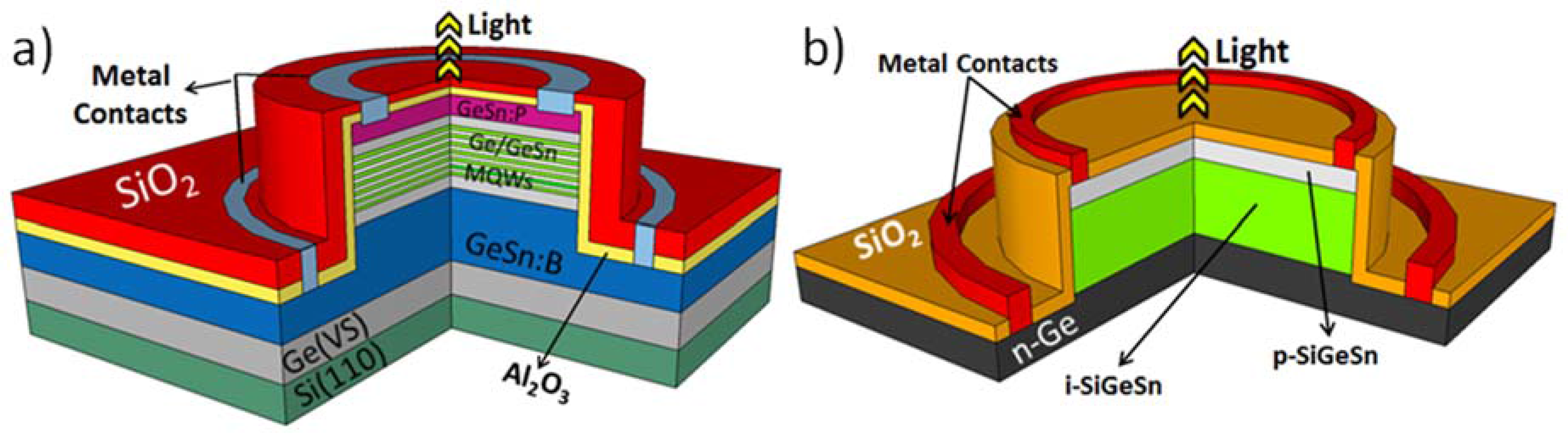
2. Light Emitters Based on Group IV Materials

Among all of the approaches used to develop Ge-based light emitters, strain engineering is a prominent one because it allows the modification of the electronic band structure, lifting degeneracies at high symmetry points of the reciprocal space and suppressing intervalley scattering. These ideas have been originally applied to group IV semiconductors to enhance carrier mobility for improving MOSFET performances [38,39,40].
As mentioned before, Ge is characterized by an indirect gap, whose value at low temperatures is EL = 0.744 eV. The absolute minimum of the conduction band (CB) lies at the four equivalent L-points of the Brillouin zone (L-valley). Other relative CB minima are located at the Γ (Γ-valley) and X (X-valley) points at 0.898 eV and 0.920 eV above the top of the valence band (VB), respectively [41]. The VB maximum occurs at the Γ point and consists of two degenerate heavy hole (HH) and light hole (LH) bands (see Figure 1a). Spin-orbit interaction leads to an additional hole band, termed the split-off (SO) band, at about 0.29 eV below the VB top. A schematic representation of the Ge band structure is demonstrated in Figure 1a.
Strain can notably modify the electronic structure, as shown in Figure 1b by an eight-band k·p calculation carried out in the vicinity of the zone center. Theory furthermore predicts that the direct gap demonstrates a more pronounced strain-induced redshift than the indirect gap, so that for a tensile strain in the (001) plane of about 2% Ge becomes a direct semiconductor with a bandgap amplitude close to 0.5 eV [20]. The extension of the spectral range of Si photonics into the mid-infrared (MIR) range (e.g., 2–5 μm) is highly desired for many applications, such as chemical and biological sensing, medical diagnostics, environmental monitoring, active imaging and free-space laser communications [42,43,44]. It should be noted that the indirect-to-direct crossover has been predicted to occur also in the case of uniaxial stress, even though this requires strain values as high as ~4% along the (001) and (111) crystallographic directions [45,46]. Although theoretical studies disclosed the promising role of tensile strain already some decades ago [20,45,47,48], its experimental implementation received very little attention and remained beyond reach until very recently. The demonstration of a working Ge laser [22] tantalized indeed the interest of a soaring number of research groups, sparking a worldwide race for improving the laser design by pushing the boundaries of the experimentally-attainable strain.
Strain can be conveniently obtained via epitaxial growth of a Ge layer on Si. After cooling from sufficiently high deposition temperatures, a tensile strain smaller than 0.3% is spontaneously induced in the epitaxial layer thanks to the difference in the thermal expansion coefficients between Ge and the thick Si substrate. This amount of strain, albeit very small, is nevertheless useful: various Ge-based LEDs and photodiodes were successfully fabricated on Si (see for instance [49,50,51,52,53] and a typical layout in Figure 2a). It is worth noting that the combination of the weak thermal strain and high n-type doping was indeed the key enabling factor in the first observation of room temperature laser emission under optical [22] and electrical injection [24].
A 0.25% tensile strain reduces the energy difference between the Γ- and L-valleys from 140 to 115 meV. Further compensation can be provided by filling L-valley states via n-type doping, as proposed by Liu et al. [54]. An impurity concentration of about 7.6 × 1019 cm−3 would suffice in equalizing Γ- and L-valley occupancy. This can mitigate the naturally occurring Γ-to-L intervalley scattering and, owing to the higher transition rate, favor radiative recombination events via the direct gap. The beneficial role played by tensile strain and n-type doping in enhancing direct gap emission, albeit subtle (see [55,56]), has been pointed out by different authors [57,58,59,60,61].
It should be noted, however, that the enhancement of the direct bandgap emission does not necessarily imply that optical amplification can be achieved. Indeed, the very high density of extrinsic carriers due to the requested high n-doping level can drastically decrease the net optical gain. Parasitic carrier loss channels might therefore lead to unacceptably high threshold current densities (about 105 A/cm2). The optical gain had been first observed in the wavelength range of 1600–1608 nm near the direct bandgap, and a maximum gain coefficient of about 50 cm−1 was measured at 1605 nm [62]. Such a value is two orders of magnitude lower than the first theoretical evaluations [47]. The original description of the mechanisms leading to stimulated emission in Ge was indeed put under severe scrutiny [63], boosting several theoretical works [47,64,65,66] aimed at accurately evaluating gain/loss mechanisms in an effort to guide experimental investigations. More recently, the high threshold current problem was investigated in [67]. According to these findings, n-doping yields only a modest improvement under the low strain regime, and the threshold current remains in the hundreds of kA/cm2 regime. As a comparison, undoped Ge would possibly require a lower current density at a biaxial strain level of ~1.3%, i.e., well below the indirect-to-direct crossover. Presently, there is certain consensus on the fact that heavy doping is not the most efficient way to achieve a sizeable amplification of the optical field, if current densities have to comply with the specifications of state-of-the-art microelectronic devices [67].
Many alternatives focused on extending the limit of the attainable strain have thus promptly emerged. As shown before, strain engineering was chiefly based on heteroepitaxy. However, the tensile strain required to make Ge a direct bandgap material turns out to be significant. Above all, it imposes a contrasting requirement on the deposition template, namely a substrate with a lattice constant sufficiently larger than the one of Ge whilst enabling the possibility of growing the desired layer thickness without incurring in the unwanted nucleation of dislocations. Such growth defects provide plastic strain relaxation and competing nonradiative recombination channels [68].
Materials with a lattice constant close to, but somewhat larger than that of Ge, such as InGaAs, have been investigated [69,70]. A biaxial tensile strain of 2.33%, i.e., above the onset for direct-bandgap behavior, was reported in a 10 nm-thick Ge film pseudomorphically grown on a graded In0.4Ga0.6As substrate [69]. A large increase in the overall photoluminescence (PL) peak intensity relative to an unstrained Ge sample was demonstrated (greater than 20×) at cryogenic temperatures, with the transition energy estimated to be around 0.74 eV. However, no definite proof of directness was provided [70].
A different approach relies on stressors. These consist of a layer of a material, like silicon nitride or tungsten, overgrown under large compressive strain on a Ge membrane. By doing so, the layer transfers its load to the underlying Ge film, inducing therein a tensile strain. Depending on the geometry, different values of the equivalent biaxial strain were reported so far for SiN stressors, such as 0.7% in micro-stripe structures [71,72]. A strain value of 1.35% has been reported for SiN all-around stressed Ge nanopillars [73] and 1.5% in Ge microdisks [74]. Very recently, an indirect-to-direct transition has been observed for this geometry, by applying tensile strain up to 1.75% [75], and the room temperature PL intensity increased by two orders of magnitude. On the other hand, by depositing 80 nm of tungsten on a 1.16 µm-thick Ge layer, a biaxial tensile strain up to 1.13% has been obtained [76,77].
Photodiodes [76] and LEDs [77] based on this technology were fabricated, as schematically shown in Figure 2b. The responsivity and emission spectra could be red-shifted through the deposition of stressor layers of increasing thickness. The LED forward current was found to increase with the applied tensile strain, a behavior that was attributed to the expected increased intrinsic carrier concentration and enhanced carrier mobility caused by the strain-induced bandgap reduction. Yet at room temperature, the current density remains large, i.e., approximately 250 A/cm2 [77]. Another approach consists of utilizing SiGe directly deposited on Ge. After epitaxial growth, SiGe is patterned in a ridge-like design via a top-down processing based on electron beam lithography and reactive ion etching (Figure 2c). With this technique, the fabrication of free surfaces in the compressed SiGe cap allows strain relaxation and the transfer of a tensile load to the Ge regions in between two adjacent SiGe stripes [78]. By doing so, a local uniaxial tensile strain as high as 4% can be obtained [78]. Such a technique is quite versatile, as it offer different designs and orientations of the SiGe pattern, thus enabling one to tailor the strain from uniaxial to biaxial in a wide range of values [79].
Uniaxially-strained Ge layers have been also fabricated by taking advantage of the thermal mismatch between Si and Ge [58]. At variance from the previously-described methods, constricted Ge suspended microbridges were patterned using electron-beam lithography, as reported in Figure 2d. Then, dry etching of the Ge layer and a selective wet etch of the material underneath (either Si or SOI) were performed to release the Ge from the substrate. Since stress is inversely proportional to the cross-sectional area of a microbridge, the freestanding constricted regions experience a much larger tensile strain compared to the thermally-strained Ge slab. Uniaxial strain values up to 3.1% were obtained alongside a concomitant 210 meV shift of the PL peak with respect to bulk material and a strong increase (25×) of the spectrally-integrated PL intensity [58]. Very recently, this method offered the possibility to systematically explore the high strain regime, leading to a detailed investigation of deformation potentials and nonlinearities occurring for Raman modes and the energy gap [80,81,82].
Finally, Ge can be strained by utilizing external mechanical stress. This approach is attractive for basic studies, as well as device applications, since it allows the control of the material properties simply by varying the applied stress. The use of mechanical stress to enable optical gain has been investigated numerically by Lim et al. in [83]. The geometry considered in that study consists of a cross-shaped suspended Si platform supporting a Ge disk at its center. In the presence of a vertical force of 330 mN applied at the platform center, where the Ge active layer resides, a maximum biaxial tensile strain of about 2.7% is expected. This geometry should therefore be suitable for the development of direct bandgap LEDs. In addition, a strain-tunable wavelength range of 400 nm opens up the possibility to get a tunable light source integrated on Si. The approach based on an external mechanical stress was experimentally implemented by El Kurdi et al. [84] using a 28 µm-thick Ge sheet obtained after chemical etching of a bulk wafer. However, further benefits are expected from the use of nanomembranes, which, owning to a reduced layer thickness, can mitigate the possible issues arising at large strain because of plastic relaxation and concomitant defect formation [85]. This technology is based on the complete or partial release of a semiconductor layer, with a thickness of a few tens of nm, from its original substrate via the selective etching of an underlying sacrificial layer. When completely released, the Ge membrane can be transferred and bonded onto a variety of substrates. Nanomembranes offer novel opportunities for strain engineering, both through spontaneous elastic strain and through the external application of mechanical stress. In recent works [42,86,87], biaxial tensile strain sufficiently large to create a direct bandgap has been realized, but still no unambiguous proof of directness has been demonstrated.
Alloying provides another research strategy. In this context, germanium-tin (GeSn) has attracted a great deal of attention [88]. The reason for such an interest can be traced back to the fact that the incorporation of Sn into the Ge lattice mimics the effects of tensile strain, perturbing the bandgap and shifting the Γ-valley at lower energies. Above all, an indirect-to-direct bandgap transition is expected to occur at a certain critical Sn molar fraction [20,21].
Experimental investigations of binary GeSn alloys lagged well behind those on strained Ge because of the fundamental limitations imposed by the very poor Sn solubility in Ge (less than 1%) [89] and by the inherently large lattice constant of Sn, resulting in a mismatch of about 15% with Ge [88]. The first monocrystalline GeSn epitaxial layers were indeed based on out-of-equilibrium growth techniques, such as low-temperature molecular beam epitaxy [90,91,92] and magnetron sputtering [93]. Seminal works relying on the chemical vapor deposition (CVD) growth technique demonstrated the possibility to obtain samples with excellent structural and optical quality [88,94,95,96]. Remarkably, these findings turned out to be crucial because they put forward the use of CVD, which is routinely utilized for large-scale production in semiconductor foundries. Nevertheless, it was only the very recent substitution of the original SnD4 precursor with SnCl4, a stable commercially available liquid source [97], that has finally opened the door to a full exploitation of the novel and advanced optical properties of these intriguing materials. The first PL studies focused on Ge-rich alloys in an effort to explore the indirect-to-direct transition and to clarify the band structure dependence on experimental parameters, such as Sn molar fraction [98], doping [99], temperature [100] and strain [101,102]. These research efforts lead to the first observation at cryogenic temperature, i.e., below 90 K, of laser action under optical pumping in CVD-grown GeSn with Sn content of 12% [23]. Such a milestone settled down the debate about the realization of a group IV direct bandgap material, although recent findings [103] have pointed out that the temperature-dependent PL characteristic, as put forward in [23], is not sufficient to unambiguously unveil the direct nature of the bandgap. New investigations focused on refinements of the optically-injected GeSn laser; indeed, stimulated emission up to 130 K has been reported in microdisks [104] and up to 110 K in tailored ridge waveguide structures [105].
The creation of working photodiodes can be regarded as a preparatory step towards the realization of an electrically-injected device. Prototype nip heterostructures were initially studied using GeSn active layers directly grown on p-type Si(100) [106]. This device was shown to exhibit enhanced responsivities, tunable absorption edges and an extended IR coverage beyond that of Ge into the MIR. A direct-gap electroluminescence (EL) signal was also reported, pointing out the potential of this class of materials. Improved emission was subsequently obtained by using a Ge-buffer layer, which introduces a separation between the active device and the Ge/Si interface [107,108,109,110]. These devices were fabricated as pn Ge/GeSn junctions [110] or in a double heterostructure p-i-n geometry [108,111], directly on Ge or on Ge-buffered Si substrates. The Sn concentrations of the active regions varied from 2%–9%, while the layer thickness was kept below 300 nm, eventually suggesting that the fabrication of LEDs with a tunable response in the MIR is within reach.
Recent works comparing different emission efficiencies from GeSn diodes grown on Ge buffers show evidence of a substantial droop as a function of Sn concentration [112]. This has been ascribed to the emergence of strain relaxation. One of the major issues with LED designs is the nonradiative recombination, which is caused by dislocations originated at the interfaces between the thick GeSn layer and the strain-relaxed Ge buffer. Lattice constant engineering has been thus explored as a viable path to tackle this problem. In particular, the Ge layers were replaced by Ge-richer GeSn alloys in order to ensure carrier confinement and to promote light extraction. On the other hand, the Sn imbalance was kept small enough to prevent massive dislocation injection [113]. These diodes adopt a conventional design, in which the active region is sandwiched between a buffer and a Ge capping layer.
Even though the strain relaxation issue appears to be manageable in the GeSn system, a potential additional problem in the direct gap regime is the low thermal stability associated with high Sn contents. These alloys are likely to be metastable, and at high temperatures, they tend to decompose via surface segregation and phase precipitation of Sn, compromising device functionality and structural integrity. Yet, such a serious challenge has not been fully addressed in the literature. It should be noted, however, that the first p-i-n device with Sn concentration up to 15% was realized [114]. The active undoped GeSn layer presented an indirect gap owning to the residual compressive strain induced by the underlying Ge-richer Ge89Sn11 n-doped buffer. In addition, the electronic band alignment between these two alloy layers turned out to be of type II. Under this condition, electrons and holes are spatially separated at the opposite sides of the heterojunction, thereby reducing the radiative recombination events.
An alternative to GeSn is represented by the SiGeSn ternary analogue, which should possess an enhanced stability due to the increased mixing entropy associated with Si incorporation into the lattice [115]. Recalling III–V compound semiconductors, SiGeSn is meant to be attractive because its energy band structure is expected to be designed independently on the lattice constant via a straightforward control of the molar fractions of the alloy components [96,116]. At a first glance, the composition of SiGeSn can be adjusted in order to obtain, in principle, a direct gap energy ranging from 0.2–0.6 eV [116]. To date, SiGeSn alloys have a larger bandgap compared to the binary GeSn alloys. This makes them suitable as barrier layers in quantum well stacks (Figure 3a) [117] and in a double heterostructure geometry [118]. Noteworthy, SiGeSn might offer thermally-robust alternatives to GeSn light sources. A prototype of SiGeSn light-emitting diodes with direct and indirect edges has also been demonstrated (see the device layout reported in Figure 3b) [119]. This first-generation device showed diode current-voltage characteristics and absorption edges that in analogy to GeSn alloys red-shift with increasing Sn content, covering all telecom bands and beyond.

3. Spintronics Based on Group IV Materials

3.1. Optical Investigations of the Spin Physics of Group IV Materials

In 1968, Lampel carried out a pioneering work [25] proving that at 77 K, the polarization of nuclear spins induced in Si, by photogenerating CB electrons via circularly-polarized light, was 8.5-times larger than the maximum achievable by using the, at that time conventional, Overhauser effect. A compelling evidence of band-to-band optical pumping of spin-polarized electrons in semiconductors was indeed provided a year later. In 1969, Parsons [120] successfully measured the low-temperature spin polarization and spin lifetime of electrons in p-doped GaSb, by leveraging polarization-resolved PL and the Hanle effect, i.e., the PL circular polarization dependence upon an external magnetic field.
The breakthrough studies of Lampel and Parsons put forward optical orientation, that is the generation of a non-equilibrium spin population by means of circularly-polarized light absorption, as a prominent technique to provide direct access to the spin properties of semiconductors. As elucidated by the important book by Zakharchenya and Meyer [121], optical orientation yielded a pivotal contribution to gain a deeper understanding of spin-dependent phenomena primarily in direct gap III–V compounds. Noteworthy, such a technique was not fully applied to group IV materials, which were wrongly disregarded because of their inherent indirect bandgap and the consequent poor light absorption and emission efficiencies [122]. Before the late 2000s, only Allensbach and coworkers studied the spin properties of CB electrons in Ge by means of the photoemission technique via absorption of circularly-polarized light [123]. In this work, a Cs-coated Ge(001) crystal was utilized as a proof of principle of an approach to experimentally determine the orbital wave function mixing caused by the spin-orbit interaction of electronic states possessing a different symmetry.
In spite of the initial challenges imposed on the optical investigations by the subtleties of the band structure, it was soon recognized that group IV semiconductors might have a unique potential in the field of spintronics. Indeed, their centrosymmetric crystal structure guarantees intrinsically long spin lifetimes, as it prevents spin relaxation due to the Dyakonov–Perel mechanism, which is otherwise important in the direct gap III–V counterpart [124]. In addition, the natural abundance of zero-spin nuclear isotopes further reduces hyperfine interactions and lengthens the spin coherence time [122,124,125,126]. Such motivations, alongside additional benefits, such as a sizeable spin-orbit interaction and a feasible monolithic integration in the microelectronics technology, recently led Ge to gain new momentum within the research community. Above all, Ge turns out to be an interesting SOE candidate also because of its quasi-direct behavior and its close similarity with the III–V band structure at the center of the Brillouin zone. This paved the way to the exploitation of optical orientation as a viable tool to investigate spin-dependent phenomena occurring in Ge. All-optical spin injection in (111)-oriented bulk Ge was indeed addressed by Loren et al. [26], who were able to demonstrate the injection of pure spin currents via quantum interference between one and two photon absorption. In addition, an experimental estimation of the Γ-to-L intervalley scattering time was reported, in good agreement with the value of (230 ± 25) fs previously measured at 295 K via time-resolved transmission experiments on bulk Ge [127]. Some years later, ultrafast time- and polarization-resolved pump-probe differential transmission demonstrated the spin relaxation of holes in Ge to be of about 700 fs at room temperature [128].
In the meantime, Rioux and Sipe carried out the first detailed theoretical investigations of the optical spin orientation in bulk Ge by using a refined 30-band k∙p method [129]. They demonstrated that the degree of spin polarization (DSP) is 50% (−83.3%) for electrons (holes) at the direct gap energy threshold (i.e., 0.89 eV), as expected by considering the atomic-like character of the zone center energy levels. It was also shown that the spectral dependence of the electronic DSP, as summarized in the left panel of Figure 4 mimics the one of GaAs [130] and decreases at the onset of the absorption from the SO band. This behavior was shown to be mainly caused by the LH rather than the commonly argued transitions related to the SO band [129]. Interestingly, at 2.3 eV, the calculations demonstrated a sizeable DSP, i.e., >20%, whose origin stems from the enhanced joint density of states between conduction and the HH band at the E1 critical point [129]. The spin polarization of holes was found to be well above 80% and to sharply decrease when the excitation energy is increased by 50 and 80 meV above the direct absorption edge. At such photon energies, the coherence between the HH and LH hole states is lost because their splitting reaches a cut-off value of 30 meV [129].
Magneto-optics experiments proved to be useful to study the spin dynamics of Ge [131,132,133]. Time-resolved Faraday rotation experiments, carried out at 8 K on a (111)-oriented and undoped Ge wafer, evidenced two different mechanisms governing the spin precession. A high-frequency and large-amplitude rotation component was shown to rapidly decay after about 50 ps, while a second one persisted beyond 200 ps [131]. The former (latter) was ascribed to the Larmor precession of the hole (electron) spin. The coherence time of the spin ensemble of holes was found to markedly depend on the external magnetic field and excitation power density, approaching 150 ps in the absence of a magnetic field and for a density of photo-excited carriers of 1014 cm−3 [131]. Finally, an effective hole g-factor of 5.5 was derived. The ensemble spin coherence time of electrons was pointed out to exceed 1 ns and to be constant for a wide range of carrier densities and for temperatures up to 60 K [131]. The effective electron g-factor for bulk Ge was inferred to be about 1.83 [131], in reasonable agreement with available electron spin resonance data and theoretical predictions [134,135].
A novel and sensitive radio-frequency (rf) modulation technique relying on optical orientation [136] was introduced to detect spins in (100)-oriented n-doped bulk Ge by Guite and Venkataraman [27]. In this work, a magnetic field of few mT was sufficient to observe Hanle depolarization. Such fields are weaker than the one needed for GaAs, stemming from a longer spin lifetime ( T S ) . A maximum spin orientation efficiency of 4.8% was shown for Ge, and a T S = ( 4.6 ± 1.0 )   ns was derived at 127 K by assuming an effective g-factor of 1.6. The same experimental technique was then employed to address the temperature dependence of the spin lifetime, which in the 100–180 K temperature range was demonstrated to decrease monolithically from 5 ns to 2 ns [137]. Such a result was explained in terms of the Elliot–Yafet (EY) mechanism and shown to be in good agreement with theoretically-calculated values of the intrinsic spin relaxation time. Such calculations include electron-phonon scattering and were obtained by expansion of a spin-dependent k·p Hamiltonian in the vicinity of the L point [138].
The optical orientation process in bulk Ge was systematically investigated by comparing polarization-resolved PL of the direct gap transition and Monte Carlo calculations over a wide doping and temperature range [139]. This offered insights into the spin and energy relaxation mechanisms of the out-of-equilibrium ensemble of spin-polarized electrons. It was shown that two electron populations with spin pointing in opposite directions can be simultaneously photogenerated nearby the zone center by infrared excitation at 1.17 eV. Notably, these two spin populations have a different excess energy in the CB. Temperature and doping conditions were crucial in modifying the carrier kinetics and in determining the final helicity of the direct gap PL [139]. An example of a complete reversal of the circular polarization degree for a p-type Ge:Ga wafer at the critical temperature of about 70 K is shown in Figure 5a. Such findings were explained by pointing out the role of energy relaxation through the satellite X-valleys [139], largely underestimated in previous literature works. Polarization-resolved PL measurements of a (001)-oriented, nominally intrinsic, bulk Ge demonstrated a cross-polarized helicity for the direct and indirect bandgap recombinations, unveiling an intriguing valley-dependent spin polarization [140]. The latter stems from the rich spin dynamics of electrons in the multivalley CB of Ge [140]. By gathering access to the indirect gap recombination, this work provided, in addition, an experimental proof of the spin-dependent selection rules theoretically predicted for phonon-mediated optical transitions in Ge [141].
Such results point towards a long spin lifetime, namely in the hundreds of ns range in the low temperature regime, as experimentally confirmed by experimental observations of different research groups [133,140,142]. Yet, such findings fall well-below theoretical values [138,143], demonstrating the opening of relaxation channels that limit the observable spin lifetimes in bulk material at cryogenic temperatures and outweigh the intrinsic EY relaxation mechanism. A recent survey of the existing literature spin lifetime data is reported in [140].
The possible origin of these extrinsic processes lies in the subtle role played by impurities. Song et al. [144] put forward a donor-driven spin relaxation, in which the spin flip of CB electrons is governed by scattering off the central-cell potential of the impurity. This mechanism can be expected to be effective at relatively high donor concentrations. A more recent work shed light on an additional process [145]. By combining spin transport measurements and theoretical modeling, it was shown that the exchange with donor impurity-bound electrons emerges in semiconductors such as Si in the low temperature regime, and dictates the spin relaxation of CB electrons by prevailing over the intrinsic EY process even in high purity samples.
In a recent paper, the dynamics of spin-polarized carriers in Ge was further addressed via photoluminescence excitation (PLE) spectroscopy [146]. By using a tunable laser source, a PL circular polarization degree of about 22% was reported for excitation photon energies close to the direct gap of a high p-doped sample (see Figure 5b). This is in good agreement with the DSP expected in bulk Ge (Figure 4).
It is worth noticing that in the low doping regime, the fraction of electrons suffering Γ-X-Γ scattering is expected to be reduced, thus decreasing the average lifetime of electrons recombining radiatively via the direct gap transitions. This mechanism possibly leads to the breakdown of the standard assumption of a negligible hole spin polarization and results in a circular polarization degree of the PL as high as 35% [146]. In [146], a direct observation of resonant electronic Raman scattering (ERS) was also reported and utilized to reconstruct the VB dispersion.
Besides enhancing the direct gap recombination, as discussed in the previous section, strain was pointed out also as an effective degree of freedom for tailoring the spin-dependent phenomena. Indeed, theoretical works predicted the possibility to remove the valley degeneracy, thus suppressing an important spin relaxation channel due to intervalley scattering, eventually lengthening the spin lifetime and diffusion length [138,143].
The optical orientation process in compressively-strained Ge epilayers was initially explored by means of photoemission spectroscopy [147,148,149]. These studies demonstrate that, owing to the strain-induced HH-LH splitting, it is possible to enhance the LH-SO orbital mixing along the growth direction. This improves the DSP up to 62%, i.e., above the 50% bulk limit for an unstrained sample. A further optimization of compressive strain leads subsequent works to achieve a spin polarization of 72% in Si0.18Ge0.82/Si0.4Ge0.6 heterojunctions [150,151]. In this case, the vacuum energy level was notably lowered below the CB edge, thus allowing access to photoemitted electrons resulting from HH to CB band transitions at the Γ point.
The impact of biaxial tensile strain on the spin-dependent direct-gap radiative recombination was studied by Vitiello et al. utilizing epitaxial Ge-on-Si(001) heterostructures [152]. In this work, a set of samples characterized by different doping, but the same tensile strain, was addressed, demonstrating a record-high PL polarization degree of 85% at low temperatures for a not-intentionally doped sample. First-neighbor tight-binding (TB) calculations including strain-induced effects clarified that the DSP for CB electrons optically coupled to SO states is 90%, in striking agreement with the experimentally-reported PL data [152]. This further corroborated the physical picture according to which, in the low doping regime, the direct gap recombination is dominated by the small fraction of electrons optically coupled to the SO states, whereas electrons excited from HH and LH VB states possess a large kinetic energy and are more likely to be scattered out of the zone center.
Epitaxial Ge-based heterostructures open interesting perspectives towards the implementation of photonics architectures with a tunable emission wavelength. In this context, optical and structural properties of Ge-based multiple quantum well (MQW) heterostructures have been widely studied throughout the last decade [153,154,155,156,157,158,159]. Nevertheless, it was only during the last few years that their spin-dependent properties were actually addressed. In this respect, Virgilio and Grosso [160] explored for the first time the possibility of attaining optical spin orientation in strained-balanced Ge/SiGe MQWs. The DSP dependence on the photon energy was derived by means of TB calculations, and an almost full polarization, i.e., 96%, was shown in correspondence of the HH1-cΓ1 transition (see the right panel in Figure 4). This result stems from the removal of the HH-LH VB degeneracy due to the combined effect of strain and quantum confinement. Notably, as opposed to III–V QWs, no sign inversion of the electron spin polarization, but rather a DSP minimum, was pointed out at the LH1-cΓ1 energy threshold (Figure 4). Such a finding differs, however, from subsequent experiments, which exploited polarization-resolved HH1-cΓ1 PL as a function of the well width and demonstrated a complete reversal of the PL helicity by sweeping the excitation energy throughout the LH absorption [161].
The first experimental study of the spin lifetime of both optically-pumped holes and electrons in Ge QWs was, however, carried out in 2012 [28]. In particular, an electron spin lifetime longer than 5 ns was inferred by a direct comparison of the temperature-dependent indirect gap transitions and k∙p simulations of the intrinsic relaxation mechanisms. The polarization analysis of the direct gap emission was also used to investigate the spin lifetime of holes. It was shown that spin relaxation of LH takes place on a time scale faster than the electron intervalley scattering time, namely 0.5 ps [162]. The opposite holds for the HH band, who suffers a large depolarization contribution due the parity conserving scattering events guiding the LH energy relaxation.
Such a ultrafast hole spin dynamics was then confirmed and addressed in detail in Ge/SiGe QWs by means of a white-light pump-probe method [163]. The unique possibility to lift HH-LH degeneracy was pointed out to be useful in avoiding mixing of the VB states. A robust DSP of 80% was thus attained along with a spin relaxation time for HH up to 2.1 ps at 10 K.
A very recent work proposed to avoid doping-induced relaxation of conduction band carriers by spatially separating itinerant electrons from their parent donor atoms via remote doping in the SiGe barriers [164]. This has led to the observation of a drastic increase of the low temperature spin relaxation time of Ge MQWs compared to high purity Ge wafers. In addition, ref. [164] put forward the beneficial role of confinement in further contributing to the suppression of the impurity-induced spin relaxation channels and notably provided the first experimental demonstration of the confinement-induced control over the g-factor of the conduction band electrons in Ge, as theoretically predicted a decade ago [165]. Owning to spin-orbit coupling, Ge offers indeed a larger g-factor tuning range than Si. This opens unexplored pathways for future studies of confinement-induced tailoring of the spin physics in technologically relevant materials, such as group IV semiconductors.

3.2. Electrical Spin Injection in Ge

A spin-based light-emitting device should ideally consist of a semiconducting core where spin-oriented carriers, injected by means of magnetic polarizing contacts, recombine, radiatively generating photons with a well-defined angular momentum. Owning to the constraints on the spin injectors, the amplified or stimulated emission can be extracted from the optically-active medium through an aperture in the top or bottom contacts (vertical cavity surface emitting laser, i.e., VCSEL) or through a side facet (slab laser) [166]. Whilst it is not necessary that both types of carriers are spin-polarized, the more stringent requirement for any practical implementation of circularly-polarized light sources is the efficient electrical spin injection at room temperature without high external magnetic fields.
Electrical spin injection in Ge lagged behind the earlier studies on Si [37] and developed around two classes of contact materials, i.e., diluted magnetic semiconductors (DMS) and ferromagnetic materials (FM). The studies focused on DMS contacts were primarily concerned with the search for materials with good thermal and magnetic stability at room temperature and exhibiting a ferromagnetic behavior that guarantees high polarization of the injected carriers. Many different alloys have been investigated, namely MnFeGe [167], FeGe [168], FeSi [169] and MnGe [170,171]. For information about the material characteristics, we recall about [172]. Spin accumulation in Ge using DMS-based Schottky tunnel contacts was first demonstrated in a Co/FeSi/n-Ge structure [173]. The results evidenced deviations from the diffusion model, possibly due to inhomogeneous doping distribution. A second work by Hamaya and coworkers [174] succeeded in observing evidence of spin accumulation in a similar structure without the Co layer. These investigations highlighted the importance of the interface and material quality to avoid uncontrolled fluctuations in the interface resistance, which may affect the magnitude of the spin accumulation in the semiconductor channel. The use of MnGe later on enabled the observation of large voltages, heralding successful spin accumulation, and the measurement of a significant figure of merit, such as a spin-resistance-area product (spin-RA) of ≈100 Ω·μm2 up to 200 K [175]. The clear-cut evidence of electrical spin injection using DMS was given by Kasahara and coworkers in [176]. They measured 12% efficiency of spin injection, which doubled the one reported in structures with Fe/MgO contacts at that time, and resulted in a spin diffusion length (λs) of 0.6 μm. In the meantime, spin accumulation in n-Ge at room temperature was reported in a FeSi/n-Ge structure [177]. These recent results demonstrate that DMSs have intriguing prospects for yielding efficient electrical spin injectors in Ge. However, it is important to notice that, up to now, these materials have been successfully grown only on top of (111) Ge, due to the lattice match between the DMS and the semiconductor. Such a requirement might hinder large-scale applicability in commercial devices that typically rely on the more conventional (001) surface orientation.
A similar limitation does not concern FM contact devices, which to date proved to be the most successful device architectures for III–V and group IV materials. The study of FM/Ge stacks followed shortly the demonstrations of spin injection in Si [37,178] and were promptly improved by adding a thin insulating layer between the FM and the Ge wafer. A similar structure realizes a tunnel contact for the injected carriers, preventing the Fermi level pinning at the interface [179] and resolving the conductivity mismatch between the FM and the semiconductor [180]. Several studies were carried out on the oxides’ efficiencies in magnetic tunnel junctions [181,182] and on the structural and electrical quality of the oxide deposition on Ge substrates, identifying materials and manufacturing processes improving the spin-selective tunnel process [183,184]. Among all, MgO has been the most investigated dielectric for realizing spin injection [185,186,187].
The first evidence of spin accumulation in Ge was reported by Saito et al. [188], who observed the Hanle effect up to 100 K in p-type Ge, carrying out measurements by means of a Fe/MgO contact in three-terminal geometry, and reporting a spin polarization of ≈4.4%. Saito and coworkers noticed that the measured spin signal was much larger than the value predicted from the commonly-used diffusion model, similarly to the observations reported in Si [189]. Afterwards, several spin accumulation results appeared in the literature in disagreement with the diffusion theory [190,191,192]. A part of these findings was explained by the presence of localized states at the oxide/Ge interface [190]. The other results stimulated improvements in the theoretical description of FM/insulator/non-magnetic junctions and were recently described by Song et al. in [193]. Yet, the debate about the actual mechanisms leading to spin injection is still on-going [194].
Measurements performed using a three-terminal device pointed out spin accumulation also in n-type Ge in a Co/Py/Al2O3/Ge structure up to 220 K [190]. Importantly, in this work, the authors identified a source of spin relaxation in the random fields arising from interface roughness, thus highlighting the crucial role of oxide/Ge interface quality in electrical spin injection. A following study, confirming this effect, reported an additional and competing depolarization mechanism due to magnetic stray fields localized at the interface, due to the proximity of the FM contact [195]. Quite quickly, the use of FM tunnel contacts in three-terminal geometry allowed researchers to observe spin accumulation signals up to room temperature [196,197,198].
Dedicated investigations [199,200,201] contributed to casting doubts about the accuracy of the demonstration of spin accumulation, as provided by three-terminal device geometries (Figure 6a) and suggested the alternative exploitation of four terminal non-local devices (Figure 6b). The latter is less prone to the interface issues associated with the use of the same contact for injection and detection of spins induced in the non-magnetic material. In the meantime, important steps were made towards the observation of spin transport through the conduction states in the semiconductor. This was achieved for the first time at low temperature by spin valve measurements [202], then at room temperature by enhanced three-terminal measurements [203,204,205]. Record high transport distance and spin lifetime (about 1 μs) were obtained at T = 30 K by Li et al. [142] in the ballistic regime. Nevertheless, recent results highlighted that hot electrons might also be affected by additional spin relaxation processes [206]. Finally, the literature reports are suggesting that the resonance under microwave radiation can offer an effective method for the adiabatic pumping of spins in nonmagnetic semiconductors, such as Si and Ge, placed in direct contact with a ferromagnetic layer [12,204,207,208].
Besides the use of FM contacts for electrical spin injection, the same spin filtering properties allowed Rinaldi and coworkers to demonstrate a spin-photodiode device [209] operating at room temperature. This result constitutes an important step towards the realization of a Fe/MgO/Ge-based spin-LED.
The efforts in the field of electrical spin injection in Ge led to the recent investigation of a room temperature spin-LED [210] relying on a Fe/GeO2 contact. This device provides the first direct evidence of electrical spin injection by means of the polarized emission in Ge. Although the use of a 4 T magnetic field is needed in this device, this result points out that Ge is following shortly the achievements on Si [178] and can provide a new route in the spin-optoelectronics field. The realization of the Ge-based spin-LED can also be interpreted as a first step towards a more efficient spin-VCSEL structure, obtained to date solely in III–V compounds [166].

4. Conclusions

We reviewed the development of Ge-based light sources heralding spin-dependent properties. Such systems have the potential to introduce novel heteroepitaxial architectures, which are expected to enrich conventional microelectronic devices with photonics and spintronics benefits in terms of power consumption and processing speed. We discussed engineering approaches to tailor the optical properties of Ge in an effort to enhance radiative recombination and deliver direct bandgap materials suitable for the on-chip development of high-performance lasers. The future progress of spin-polarized light sources based on group IV materials will likely rely on spin injection utilizing ferromagnet/tunnel barrier/semiconductor structures, for which additional studies are mandatory to move from lab prototypes to the device market.
We discussed progress in the injection of spins in Ge by optical means and underlined the importance of this approach in gathering a deeper understanding of spin physics and relaxation mechanisms. Investigations based on the optical orientation process pointed out a rich spin dynamics and the compelling role of the multivalley nature of the CB of Ge in governing it. In this respect, optical investigations of spin-dependent phenomena in novel Sn-based alloys are yet untapped and might disclose puzzling phenomena, as the topological insulator characteristics of α-tin [211] seems to suggest.
While the research field reviewed here is still at an early stage, various efforts are ongoing, and the available reports have already shown the effectiveness of group IV semiconductors for implementing advanced spin-optoelectronic functionalities.

Acknowledgments

The authors would like to thank Mario Guzzi and Emanuele Grilli for the fruitful discussions and their continuous assistance. We acknowledge support from Fondazione Cariplo through Grant SearchIV No. 2013-0623.

Author Contributions

All of the authors wrote the paper. Fabio Pezzoli coordinated the work.

Conflicts of Interest

The authors declare no conflict of interest.

References

  1. Waldrop, M.M. The chips are down for Moore’s law. Nature 2016, 530, 144–147. [Google Scholar] [CrossRef] [PubMed]
  2. Wolf, S.A.; Awschalom, D.D.; Buhrman, R.A.; Daughton, J.M.; von Molnár, S.; Roukes, M.L.; Chtchelkanova, A.Y.; Treger, D.M. Spintronics: A Spin-Based Electronics Vision for the Future. Science 2001, 294, 1488–1495. [Google Scholar] [CrossRef] [PubMed]
  3. Soref, R. The past, present, and future of silicon photonics. IEEE J. Sel. Top. Quantum Electron. 2006, 12, 1678–1687. [Google Scholar] [CrossRef]
  4. Baibich, M.N.; Broto, J.M.; Fert, A.; Nguyen Van Dau, F.; Petroff, F.; Etienne, P.; Creuzet, G.; Friederich, A.; Chazelas, J. Giant magnetoresistance of (001)Fe/(001)Cr magnetic superlattices. Phys. Rev. Lett. 1988, 61, 2472–2475. [Google Scholar] [CrossRef] [PubMed]
  5. Binasch, G.; Grünberg, P.; Saurenbach, F.; Zinn, W. Enhanced magnetoresistance in layered magnetic structures with antiferromagnetic interlayer exchange. Phys. Rev. B 1989, 39, 4828–4830. [Google Scholar] [CrossRef]
  6. Awshalom, D.D.; Flatté, M.E. Challenges for semiconductor spintronics. Nat. Phys. 2007, 3, 153–159. [Google Scholar] [CrossRef]
  7. Dietl, T.; Ohno, H.; Matsukura, F.; Cibert, J.; Ferrand, D. Zener model description of ferromagnetism in zinc-blende magnetic semiconductors. Science 2000, 287, 1019–1022. [Google Scholar] [CrossRef] [PubMed]
  8. Dietl, T. A ten-year perspective on diluite magnetic semiconductors and oxides. Nat. Mater. 2010, 9, 965–974. [Google Scholar] [CrossRef] [PubMed]
  9. Dietl, T.; Ohno, H. Dilute ferromagnetics semiconductors: Physics and spintronics structures. Rev. Mod. Phys. 2014, 86, 187–251. [Google Scholar] [CrossRef]
  10. Jansen, R. Silicon spintronics. Nat. Mater. 2012, 11, 400–408. [Google Scholar] [CrossRef] [PubMed]
  11. Morton, J.J.L.; McCamey, D.R.; Eriksson, M.A.; Lyon, S.A. Embracing the quantum limit in silicon computing. Nature 2011, 479, 345–353. [Google Scholar] [CrossRef] [PubMed]
  12. Dushenko, S.; Koike, M.; Ando, Y.; Shinjo, T.; Myronov, M.; Shiraishi, M. Experimental Demonstration of Room-Temperature Spin Transport in n-Type Germanium Epilayers. Phys. Rev. Lett. 2015, 114, 196602. [Google Scholar] [CrossRef] [PubMed]
  13. Sigillito, A.J.; Jock, R.M.; Tyryshkin, A.M.; Beeman, J.W.; Haller, E.E.; Itoh, K.M.; Lyon, S.A. Electron spin coherence of shallow donors in natural and isotopically enriched. Phys. Rev. Lett. 2015, 115, 247601. [Google Scholar] [CrossRef] [PubMed]
  14. Miller, D.A.B. Rationale and challenges for optical interconnects to electronic chips. Proc. IEEE 2000, 88, 728–749. [Google Scholar] [CrossRef]
  15. O’Brien, J.L.; Furusawa, A.; Vučković, J. Photonic quantum technologies. Nat. Photonics 2009, 3, 687–695. [Google Scholar] [CrossRef]
  16. O’Brien, J.L.; Pryde, G.J.; White, A.G.; Ralph, T.C.; Branning, D. Demonstration of an all-optical quantum controlled-NOT gate. Nature 2003, 426, 264–267. [Google Scholar] [CrossRef] [PubMed] [Green Version]
  17. Tiarks, D.; Schmidt, S.; Rempe, G.; Dürr, S. Optical phase shift created with a single-photon pulse. Sci. Adv. 2016, 2, e1600036. [Google Scholar] [CrossRef] [PubMed]
  18. Liang, D.; Bowers, J.E. Recent progress in lasers on silicon. Nat. Photonics 2010, 4, 511–517. [Google Scholar] [CrossRef]
  19. Zhou, Z.; Yin, B.; Michel, J. On-chip light sources for silicon photonics. Light Sci. Appl. 2015, 4, e358. [Google Scholar] [CrossRef]
  20. Soref, R.A.; Friedman, L. Direct-gap Ge/GeSn/Si and GeSn/Ge/Si heterostructures. Superlattices Microstruct. 1993, 14, 189–193. [Google Scholar] [CrossRef]
  21. Fitzgerald, E.A.; Freeland, P.E.; Asom, M.T.; Lowe, W.P.; Macharrie, R.A.; Weir, B.E.; Kortan, A.R.; Thiel, F.A.; Xie, Y.H.; Sergent, A.M.; et al. Epitaxially stabilized GeSn diamond cubic alloys. J. Electron. Mater. 1991, 20, 489–501. [Google Scholar] [CrossRef]
  22. Liu, J.; Sun, X.; Camacho-Aguilera, R.; Kimerling, L.C.; Michel, J. Ge-on-Si laser operating at room temperature. Opt. Lett. 2010, 35, 679–681. [Google Scholar] [CrossRef] [PubMed]
  23. Wirths, S.; Geiger, R.; von den Driesch, N.; Mussler, G.; Stoica, T.; Mantl, S.; Ikonic, Z.; Luysberg, M.; Chiussi, S.; Hartmann, J.M.; et al. Lasing in direct-bandgap GeSn alloy grown on Si. Nat. Photonics 2015, 9, 88–92. [Google Scholar] [CrossRef]
  24. Camacho-Aguilera, R.E.; Cai, Y.; Patel, N.; Bessette, J.T.; Romagnoli, M.; Kimerling, L.C.; Michel, J. An electrically pumped germanium laser. Opt. Express 2012, 20, 11316–11320. [Google Scholar] [CrossRef] [PubMed]
  25. Lampel, G. Nuclear dynamic polarization by optical electronic saturation and optical pumping in semiconductors. Phys. Rev. Lett. 1968, 20, 491–493. [Google Scholar] [CrossRef]
  26. Loren, E.J.; Ruzicka, B.A.; Werake, L.K.; Zhao, H.; van Driel, H.M.; Smirl, A.L. Optical injection and detection of ballistic pure spin currents in Ge. Appl. Phys. Lett. 2009, 95, 092107. [Google Scholar] [CrossRef]
  27. Guite, C.; Venkataraman, V. Measurement of Electron Spin Lifetime and Optical Orientation Efficiency in Germanium Using Electrical Detection of Radio Frequency Modulated Spin Polarization. Phys. Rev. Lett. 2011, 107, 166603. [Google Scholar] [CrossRef] [PubMed]
  28. Pezzoli, F.; Bottegoni, F.; Trivedi, D.; Ciccacci, F.; Giorgioni, A.; Li, P.; Cecchi, S.; Grilli, E.; Song, Y.; Guzzi, M.; et al. Optical Spin Injection and Spin Lifetime in Ge Heterostructures. Phys. Rev. Lett. 2012, 108, 156603. [Google Scholar] [CrossRef] [PubMed]
  29. Oestreich, M.; Hubner, J.; Hagele, D.; Bender, M.; Gerhardt, N.; Hofmann, M.; Ruhle, W.W.; Kalt, H.; Hartmann, T.; Klar, P.; et al. Spintronics: Spin electronics and optoelectronics in semiconductors. Adv. Solid State Phys. 2001, 41, 173–186. [Google Scholar]
  30. Holub, M.; Bhattacharya, P. Spin-polarized light-emitting diodes and lasers. J. Phys. D Appl. Phys. 2007, 40, R179–R203. [Google Scholar] [CrossRef]
  31. Lee, J.; Oszwaldowski, R.; Gothgen, C.; Zutic, I. Mapping between quantum dot and quantum well lasers: From conventional to spin lasers. Phys. Rev. B 2012, 85, 045314. [Google Scholar] [CrossRef]
  32. Holub, M.; Shin, J.; Saha, D.; Bhattacharya, P. Electrical Spin Injection and Threshold Reduction in a Semiconductor Laser. Phys. Rev. Lett. 2007, 98, 146603. [Google Scholar] [CrossRef] [PubMed]
  33. Lee, J.; Bearden, S.; Wasner, E.; Zutic, I. Spin-lasers: From threshold reduction to large-signal analysis. Appl. Phys. Lett. 2014, 105, 042411. [Google Scholar] [CrossRef]
  34. Hallstein, S.; Berger, J.D.; Hilpert, M.; Schneider, H.C.; Rühle, W.W.; Jahnke, F.; Koch, S.W.; Gibbs, H.M.; Khitrova, G.; Oestreich, M. Manifestation of coherent spin precession in stimulated semiconductor emission dynamics. Phys. Rev. B 1997, 56, R7076–R7079. [Google Scholar] [CrossRef]
  35. Fiederling, R.; Keim, M.; Reuscher, G.; Ossau, W.; Schmidt, G.; Waag, A.; Molenkamp, L.W. Injection and detection of a spin-polarized current in a light-emitting diode. Nature 1999, 402, 787–790. [Google Scholar]
  36. Ohno, Y.; Young, D.K.; Beschoten, B.; Matsukura, F.; Ohno, H.; Awschalom, D.D. Electrical spin injection in a ferromagnetic semiconductor heterostructure. Nature 1999, 402, 790–792. [Google Scholar] [CrossRef]
  37. Jonker, B.T.; Kioseoglou, G.; Hanbicki, A.T.; Li, C.L.; Thompson, P.E. Electrical spin-injection into silicon from a ferromagnetic metal/tunnel barrier contact. Nat. Phys. 2007, 3, 542–546. [Google Scholar] [CrossRef]
  38. Lee, M.L.; Fitzgerald, E.A.; Bulsara, M.T.; Currie, M.T.; Lochtefeld, A. Strained Si, SiGe, and Ge channels for high-mobility metal-oxide-semiconductor field-effect transistors. J. Appl. Phys. 2005, 97, 011101. [Google Scholar] [CrossRef]
  39. Nanver, L.K.; Jovanovic, V.; Biasotto, C.; Moers, J.; Grützmacher, D.; Zhang, J.J.; Hrauda, N.; Stoffel, M.; Pezzoli, F.; Schmidt, O.G.; et al. Integration of MOSFETs with SiGe dots as stressor material. Solid-State Electron. 2011, 60, 75–83. [Google Scholar] [CrossRef]
  40. Schmidt, O.G.; Eberl, K. Self-Assembled Ge/Si Dots for Faster Field-Effect Transistors. IEEE Trans. Electron. Dev. 2001, 48, 1175–1179. [Google Scholar] [CrossRef]
  41. Richard, S.; Aniel, F.; Fishman, G. Energy-band structure of Ge, Si and GaAs: A thirty-band k∙p method. Phys. Rev. B 2004, 70, 235204. [Google Scholar] [CrossRef]
  42. Boztug, C.; Sánchez-Pérez, J.R.; Sudradjat, F.F.; Jacobson, R.B.; Paskiewicz, D.M.; Lagally, M.G.; Paiella, R. Tensilely Strained Germanium Nanomembranes as Infrared Optical Gain Media. Small 2013, 9, 622–630. [Google Scholar] [CrossRef] [PubMed]
  43. Soref, R. Mid-infrared photonics in silicon and germanium. Nat. Photonics 2010, 4, 495–497. [Google Scholar] [CrossRef]
  44. Soref, R. Group IV photonics: Enabling 2 μm communications. Nat. Photonics 2015, 9, 358–359. [Google Scholar] [CrossRef]
  45. Fischetti, M.V.; Laux, S.E. Band structure, deformation potentials, and carrier mobility in strained Si, Ge, and SiGe alloys. J. Appl. Phys. 1996, 80, 2234–2252. [Google Scholar] [CrossRef]
  46. Zhang, F.; Crespi, V.H.; Zhang, P. Prediction that Uniaxial Tension along <111> Produces a Direct Band Gap in Germanium. Phys. Rev. Lett. 2009, 102, 156401. [Google Scholar] [CrossRef] [PubMed]
  47. El Kurdi, M.; Fishman, G.; Sauvage, S.; Boucaud, P. Band structure and optical gain of tensile-strained germanium based on a 30 band k·p formalism. J. Appl. Phys. 2010, 107, 013710. [Google Scholar] [CrossRef]
  48. Pizzi, G.; Virgilio, M.; Grosso, G. Tight-binding calculation of optical gain in tensile strained [001]-Ge/SiGe quantum wells. Nanotechnology 2010, 21, 055202. [Google Scholar] [CrossRef] [PubMed]
  49. Schmid, M.; Oehme, M.; Gollhofer, M.; Körner, R.; Kaschel, M.; Kasper, E.; Schulze, J. Effect of heavy doping and strain on the electroluminescence of Ge-on-Si light emitting diodes. Thin Solid Films 2014, 557, 351–354. [Google Scholar] [CrossRef]
  50. Schwartz, B.; Klossek, A.; Kittler, M.; Oehme, M.; Kasper, E.; Schulze, J. Electroluminescence of germanium LEDs on silicon: Influence of antimony doping. Phys. Status Solidi C 2014, 11, 1686–1691. [Google Scholar] [CrossRef]
  51. Liu, Z.; Hu, W.; Li, C.; Li, Y.; Xue, C.; Li, C.; Zuo, Y.; Cheng, B.; Wang, Q. Room temperature direct-bandgap electroluminescence from n-type straincompensated Ge/SiGe multiple quantum wells. Appl. Phys. Lett. 2012, 101, 231108. [Google Scholar]
  52. Arguirov, T.; Kittler, M.; Oehme, M.; Abrosimov, N.V.; Kasper, E.; Schulze, J. Room Temperature Direct Band-Gap Emission from an Unstrained Ge P-I-N LED on Si. Solid State Phenom. 2011, 178–179, 25–30. [Google Scholar] [CrossRef]
  53. Oehme, M.; Werner, J.; Kasper, E.; Jutzi, M.; Berroth, M. High bandwidth Ge p-i-n photodetector integrated on Si. Appl. Phys. Lett. 2006, 89, 071117. [Google Scholar] [CrossRef]
  54. Liu, J.; Sun, X.; Kimerling, L.C.; Michel, J. Tensile-strained, n-type Ge as a gain medium for monolithic laser integration on Si. Opt. Express 2007, 15, 11272–11277. [Google Scholar] [CrossRef] [PubMed]
  55. Jain, J.R.; Hryciw, A.; Baer, T.M.; Miller, D.A.B.; Brongersma, M.L.; Howe, R.T. A micromachining-based technology for enhancing germanium light emission via tensile strain. Nat. Photonics 2012, 6, 398–405. [Google Scholar] [CrossRef]
  56. Boucaud, P.; El Kurdi, M.; Sauvage, S.; de Kersauson, M.; Ghrib, A.; Checoury, X. Light emission from strained germanium. Nat. Photonics 2013, 7, 162. [Google Scholar] [CrossRef]
  57. Cheng, T.-H.; Peng, K.-L.; Ko, C.-Y.; Chen, C.-Y.; Lan, H.-S.; Wu, Y.-R.; Liu, C.W.; Tseng, H.-H. Strain-enhanced photoluminescence from Ge direct transition. Appl. Phys. Lett. 2010, 96, 211108. [Google Scholar] [CrossRef]
  58. Süess, M.J.; Geiger, R.; Minamisawa, R.A.; Schiefler, G.; Frigerio, J.; Chrastina, D.; Isella, G.; Spolenak, R.; Faist, J.; Sigg, H. Analysis of enhanced light emission from highly strained germanium microbridges. Nat. Photonics 2013, 7, 466–472. [Google Scholar] [CrossRef]
  59. Lan, H.-S.; Chan, S.-T.; Cheng, T.-H.; Chen, C.-Y.; Jan, S.-R.; Liu, C.W. Biaxial tensile strain effects on photoluminescence of different orientated Ge wafers. Appl. Phys. Lett. 2011, 98, 101106. [Google Scholar] [CrossRef]
  60. El Kurdi, M.; Kociniewski, T.; Ngo, T.-P.; Boulmer, J.; Débarre, D.; Boucaud, P.; Damlencourt, J.F.; Kermarrec, O.; Bensahel, D. Enhanced photoluminescence of heavilyn-doped germanium. Appl. Phys. Lett. 2009, 94, 191107. [Google Scholar] [CrossRef]
  61. Sun, X.; Liu, J.; Kimerling, L.C.; Michel, J. Direct gap photoluminescence of n-type tensile-strained Ge-on-Si. Appl. Phys. Lett. 2009, 95, 011911. [Google Scholar] [CrossRef]
  62. Liu, J.; Sun, X.; Kimerling, L.C.; Michel, J. Direct-gap optical gain of Ge on Si at room temperature. Opt. Lett. 2009, 34, 1738–1740. [Google Scholar] [CrossRef] [PubMed]
  63. Carroll, L.; Friedli, P.; Neuenschwander, S.; Sigg, H.; Cecchi, S.; Isa, F.; Chrastina, D.; Isella, G.; Fedoryshyn, Y.; Faist, J. Direct-Gap Gain and Optical Absorption in Germanium Correlated to the Density of Photoexcited Carriers, Doping, and Strain. Phys. Rev. Lett. 2009, 109, 057402. [Google Scholar] [CrossRef] [PubMed]
  64. Virgilio, M.; Manganelli, C.L.; Grosso, G.; Pizzi, G.; Capellini, G. Radiative recombination and optical gain spectra in biaxially strainedn-type germanium. Phys. Rev. B 2013, 87, 235313. [Google Scholar] [CrossRef]
  65. Virgilio, M.; Manganelli, C.L.; Grosso, G.; Schroeder, T.; Capellini, G. Photoluminescence, recombination rate, and gain spectra in optically excited n-type and tensile strained germanium layers. J. Appl. Phys. 2013, 114, 243102. [Google Scholar] [CrossRef]
  66. Wen, H.; Bellotti, E. Rigorous theory of the radiative and gain characteristics of silicon and germanium lasing media. Phys. Rev. B 2015, 91, 035307. [Google Scholar] [CrossRef]
  67. Prost, M.; El Kurdi, M.; Aniel, F.; Zerounian, N.; Sauvage, S.; Checoury, X.; Bœuf, F.; Boucaud, P. Analysis of optical gain threshold in n-doped and tensile-strained germanium heterostructure diodes. J. Appl. Phys. 2015, 118, 125704. [Google Scholar] [CrossRef]
  68. Pezzoli, F.; Isa, F.; Isella, G.; Falub, C.V.; Kreiliger, T.; Salvalaglio, M.; Bergamaschini, R.; Grilli, E.; Guzzi, M.; von Känel, H.; et al. Ge Crystals on Si Show Their Light. Phys. Rev. Appl. 2014, 1, 044005. [Google Scholar] [CrossRef]
  69. Huo, Y.; Lin, H.; Chen, R.; Makarova, M.; Rong, Y.; Li, M.; Kamins, T.I.; Vuckovic, J.; Harris, J.S. Strong enhancement of direct transition photoluminescence with highly tensilestrained Ge grown by molecular beam epitaxy. Appl. Phys. Lett. 2011, 98, 011111. [Google Scholar] [CrossRef]
  70. Jakomin, R.; de Kersauson, M.; El Kurdi, M.; Largeau, L.; Mauguin, O.; Beaudoin, G.; Sauvage, S.; Ossikovski, R.; Ndong, G.; Chaigneau, M.; et al. High quality tensile-strained n-doped germanium thin films grown on InGaAs buffer layers by metal-organic chemical vapor deposition. Appl. Phys. Lett. 2011, 98, 091901. [Google Scholar] [CrossRef]
  71. Capellini, G.; Reich, C.; Guha, S.; Yamamoto, Y.; Lisker, M.; Virgilio, M.; Ghrib, A.; El Kurdi, M.; Boucaud, P.; Tillack, B.; et al. Tensile Ge microstructures for lasing fabricated by means of a silicon complementary metal-oxide-semiconductor process. Opt. Express, 2014, 22, 399–410. [Google Scholar] [CrossRef] [PubMed]
  72. Chahine, G.A.; Zoellner, M.H.; Richard, M.-I.; Guha, S.; Reich, C.; Zaumseil, P.; Capellini, G.; Schroeder, T.; Schülli, T.U. Strain and lattice orientation distribution in SiN/Ge complementary metal–oxide–semiconductor compatible light emitting microstructures by quick X-ray nanodiffraction microscopy. Appl. Phys. Lett. 2015, 106, 071902. [Google Scholar] [CrossRef]
  73. Millar, R.W.; Gallacher, K.; Samarelli, A.; Frigerio, J.; Chrastina, D.; Isella, G.; Dieing, T.; Paul, D.J. Extending the emission wavelenght of Ge nanopillars to 2.25 μm using silicon nitride stressor. Opt. Express 2015, 23, 18193–18202. [Google Scholar] [CrossRef] [PubMed]
  74. Ghrib, A.; El Kurdi, M.; Prost, M.; Sauvage, S.; Checoury, X.; Beaudoin, G.; Chaigneau, M.; Ossikovski, R.; Sagnes, I.; Boucaud, P. All-around SiN stressor for high and homogeneous tensile strain in germanium microdisk cavities. Adv. Opt. Mater. 2015, 3, 353–358. [Google Scholar] [CrossRef]
  75. El Kurdi, M.; Prost, M.; Ghrib, A.; Sauvage, S.; Checoury, X.; Beaudoin, G.; Sagnes, I.; Picardi, G.; Ossikovski, R.; Boucaud, P. Direct bandgap germanium microdisks obtained with silicon nitride stressor layer. ACS Photonics 2016, 3, 443–448. [Google Scholar] [CrossRef]
  76. Nam, D.; Sukhdeo, D.; Roy, A.; Balram, K.; Cheng, S.-L.; Huang, K.C.-Y.; Yuan, Z.; Brongersma, M.; Nishi, Y.; Miller, D.; Saraswat, K. Strained germanium thin film membrane on silicon substrate for optoelectronics. Opt. Express 2011, 19, 25866–25872. [Google Scholar] [CrossRef] [PubMed]
  77. Nam, D.; Sukhdeo, D.; Cheng, S.-L.; Roy, A.; Huang, K.C.-Y.; Brongersma, M.; Nishi, Y.; Saraswat, K. Electroluminescence from strained germanium membranes and implications for an efficient Si-compatible laser. Appl. Phys. Lett. 2012, 100, 131112. [Google Scholar] [CrossRef]
  78. Bollani, M.; Chrastina, D.; Gagliano, L.; Rossetto, L.; Scopece, D.; Barget, M.; Mondiali, V.; Frigerio, J.; Lodari, M.; Pezzoli, F.; et al. Local uniaxial tensile strain in germanium of up to 4% induced by SiGe epitaxial nanostructures. Appl. Phys. Lett. 2015, 107, 083101. [Google Scholar] [CrossRef]
  79. Scopece, D.; Montalenti, F.; Bollani, M.; Chrastina, D.; Bonera, E. Straining Ge bulk and nanomembranes for optoelectronic applications: A systematic numerical analysis. Semicond. Sci. Technol. 2014, 29, 095012. [Google Scholar] [CrossRef]
  80. Gassenq, A.; Tardif, S.; Guilloy, K.; Dias, G.O.; Pauc, N.; Duchemin, I.; Rouchon, D.; Hartmann, J.-M.; Widiez, J.; Escalante, J.; et al. Accurate strain measurements in highly strained Ge microbridges. Appl. Phys. Lett. 2016, 108, 241902. [Google Scholar] [CrossRef]
  81. Gassenq, A.; Guilloy, K.; Dias, G.O.; Pauc, N.; Rouchon, D.; Hartmann, J.-M.; Widiez, J.; Tardif, S.; Rieutord, F.; Escalante, J.; et al. 1.9% bi-axial tensile strain in thick germanium suspended membranes fabricated in optical germanium-on-insulator substrates for laser applications. Appl. Phys. Lett. 2015, 107, 191904. [Google Scholar] [CrossRef]
  82. Guilloy, K.; Pauc, N.; Gassenq, A.; Niquet, Y.-M.; Escalante, J.-M.; Duchemin, I.; Tardif, S.; Dias, G.O.; Rouchon, D.; Widiez, J.; et al. Germanium under High Tensile Stress: Nonlinear Dependence of Direct Band Gap vs. Strain. ACS Photonics 2016, 3, 1907–1911. [Google Scholar] [CrossRef]
  83. Lim, P.H.; Park, S.; Ishikawa, Y.; Wada, K. Enhanced direct bandgap emission in germanium by micromechanical strain engineering. Opt. Express 2009, 17, 16358–16365. [Google Scholar] [CrossRef] [PubMed]
  84. El Kurdi, M.; Bertin, H.; Martincic, E.; de Kersauson, M.; Fishman, G.; Sauvage, S.; Bosseboeuf, A.; Boucaud, P. Control of direct bandgap emission of bulk germanium by mechanical tensile strain. Appl. Phys. Lett. 2010, 96, 041909. [Google Scholar] [CrossRef]
  85. Boztug, C.; Sánchez-Pérez, J.R.; Cavallo, F.; Lagally, M.G.; Paiella, R. Strained-Germanium Nanostructures for Infrared Photonics. ACS Nano 2014, 8, 3136–3151. [Google Scholar] [CrossRef] [PubMed]
  86. Sánchez-Pérez, J.R.; Boztug, C.; Chen, F.; Sudradjat, F.F.; Paskiewicz, D.M.; Jacobson, R.B.; Lagally, M.G.; Paiella, R. Direct-bandgap light-emitting germanium in tensilely strained nanomembranes. Proc. Natl. Acad. Sci. USA 2011, 108, 18893–18898. [Google Scholar] [CrossRef] [PubMed]
  87. Boztug, C.; Sánchez-Pérez, J.R.; Yin, J.; Lagally, M.G.; Paiella, R. Grating-coupled mid-infrared light emission from tensilely strained germanium nanomembranes. Appl. Phys. Lett. 2013, 103, 201114. [Google Scholar] [CrossRef]
  88. Kouvetakis, J.; Menendez, J.; Chizmeshya, A.V.G. TIN-BASED GROUP-IV SEMICONDUCTORS: New Platforms for Opto- and Microelectronics on Silicon. Annu. Rev. Mater. Res. 2006, 36, 497–554. [Google Scholar] [CrossRef]
  89. Fleurial, J.P.; Borshchevsky, A. Si-Ge-Metal Ternary Phase Diagram Calculations. J. Electrochem. Soc. 1990, 137, 2928–2937. [Google Scholar] [CrossRef]
  90. Ragan, R.; Atwater, H.A. Measurement of the direct energy gap of coherently strained SnxGe1-x/Ge(001) heterostructures. Appl. Phys. Lett. 2000, 77, 3418–3420. [Google Scholar] [CrossRef]
  91. Kasper, E.; Werner, J.; Oehme, M.; Escoubas, S.; Burle, N.; Schulze, J. Growth of silicon based germanium tin alloys. Thin Solid Films 2012, 520, 3195–3200. [Google Scholar] [CrossRef]
  92. Schulze, J.; Oehme, M.; Werner, J. Molecular beam epitaxy grown Ge/Si pin layer sequence for photonic devices. Thin Solid Films 2012, 520, 3259–3261. [Google Scholar] [CrossRef]
  93. Pérez Ladròn de Guevara, H.; Rodrìguez, A.G.; Navarro-Contreras, H.; Vidal, M.A. Ge1-xSnx alloys pseudomorphically grown on Ge(001). Appl. Phys. Lett. 2003, 83, 4942–4944. [Google Scholar] [CrossRef]
  94. Bauer, M.R.; Taraci, J.; Tolle, J.; Chizmeshya, A.V.G.; Zollner, S.; Smith, D.J.; Menendez, J.; Hu, C.; Kouvetakis, J. Ge-Sn semiconductors for band-gap and lattice engineering. Appl. Phys. Lett. 2002, 81, 2992–2994. [Google Scholar] [CrossRef]
  95. Bauer, M.R.; Cook, C.S.; Aella, P.; Tolle, J.; Kouvetakis, J.; Crozier, P.A.; Chizmeshya, A.V.G.; Smith, D.J.; Zollner, S. SnGe superstructure materials for Si-based infrared optoelectronics. Appl. Phys. Lett. 2003, 83, 3489–3491. [Google Scholar] [CrossRef]
  96. D’Costa, V.R.; Fang, Y.-Y.; Tolle, J.; Kouvetakis, J.; Menéndez, J. Tunable Optical Gap at a Fixed Lattice Constant in Group-IV Semiconductor Alloys. Phys. Rev. Lett. 2009, 102, 107403. [Google Scholar] [CrossRef] [PubMed]
  97. Vincent, B.; Gencarelli, F.; Bender, H.; Merckling, C.; Douhard, B.; Petersen, D.H.; Hansen, O.; Henrichsen, H.H.; Meersschaut, J.; Vandervorst, W.; et al. Undoped and in-situ B doped GeSn epitaxial growth on Ge by atmospheric pressurechemical vapor deposition. Appl. Phys. Lett. 2011, 99, 152103. [Google Scholar] [CrossRef] [Green Version]
  98. Mathews, J.; Beeler, R.T.; Tolle, J.; Xu, C.; Roucka, R.; Kouvetakis, J.; Menéndez, J. Direct-gap photoluminescence with tunable emission wavelength in Ge1−y Sny alloys on silicon. Appl. Phys. Lett. 2010, 97, 221912. [Google Scholar] [CrossRef]
  99. Grzybowski, G.; Jiang, L.; Mathews, J.; Roucka, R.; Xu, C.; Beeler, R.T.; Kouvetakis, J.; Menéndez, J. Photoluminescence from heavily doped GeSn:P materials grown on Si(100). Appl. Phys. Lett. 2011, 99, 171910. [Google Scholar] [CrossRef]
  100. Ryu, M.-Y.; Harris, T.R.; Yeo, Y.K.; Beeler, R.T.; Kouvetakis, J. Temperature-dependent photoluminescence of Ge/Si and Ge1-ySny/Si, indicating possible indirect-to-direct bandgap transition at lower Sn content. Appl. Phys. Lett. 2013, 102, 171908. [Google Scholar] [CrossRef]
  101. Stange, D.; Wirths, S.; von den Driesch, N.; Mussler, G.; Stoica, T.; Ikonic, Z.; Hartmann, J.M.; Mantl, S.; Grützmacher, D.; Buca, D. Optical Transitions in Direct-Bandgap Ge1−xSnx Alloys. ACS Photonics 2015, 2, 1539–1545. [Google Scholar] [CrossRef]
  102. Gupta, S.; Magyari-Köpe, B.; Nishi, Y.; Saraswat, K.C. Achieving direct bandgap in germanium through integration of Sn alloying and external strain. J. Appl. Phys. 2013, 113, 073707. [Google Scholar] [CrossRef]
  103. Pezzoli, F.; Giorgioni, A.; Patchett, D.; Myronov, M. Temperature-Dependent Photoluminescence Characteristics of GeSn Epitaxial Layers. ACS Photonics 2016, 3, 2004–2009. [Google Scholar] [CrossRef]
  104. Stange, D.; Wirths, S.; Geiger, R.; Schulte-Braucks, C.; Marzban, B.; von den Driesch, N.; Mussler, G.; Zabel, T.; Stoica, T.; Hartmann, J.-M.; et al. Optically Pumped GeSn Microdisk Lasers on Si. ACS Photonics 2016, 3, 1279–1285. [Google Scholar] [CrossRef]
  105. Al-Kabi, S.; Ghetmiri, S.A.; Margetis, J.; Pham, T.; Zhou, Y.; Dou, W.; Collier, B.; Quinde, R.; Du, W.; Mosleh, A.; et al. An optically pumped 2.5 μm GeSn laser on Si operating at 110 K. Appl. Phys. Lett. 2016, 109, 171105. [Google Scholar] [CrossRef]
  106. Roucka, R.; Mathews, J.; Beeler, R.T.; Tolle, J.; Kouvetakis, J.; Menéndez, J. Direct gap electroluminescence from Si/Ge1−ySny p-i-n heterostructure diodes. Appl. Phys. Lett. 2011, 98, 061109. [Google Scholar] [CrossRef]
  107. Gupta, J.P.; Bhargava, N.; Kim, S.; Adam, T.; Kolodzey, J. Infrared electroluminescence from GeSn heterojunction diodes grown by molecular beam epitaxy. Appl. Phys. Lett. 2013, 102, 251117. [Google Scholar] [CrossRef]
  108. Tseng, H.H.; Wu, K.Y.; Li, H.; Mashanov, V.; Cheng, H.H.; Sun, G.; Soref, R.A. Mid-infrared electroluminescence from a Ge/Ge0.922Sn0.078/Ge double heterostructure p-i-n diode on a Si substrate. Appl. Phys. Lett. 2013, 102, 182106. [Google Scholar] [CrossRef]
  109. Werner, J.; Oehme, M.; Schmid, M.; Kaschel, M.; Schirmer, A.; Kasper, E.; Schulze, J. Germanium-tin p-i-n photodetectors integrated on silicon grown by molecular beam epitaxy. Appl. Phys. Lett. 2011, 98, 061108. [Google Scholar] [CrossRef]
  110. Oehme, M.; Kostecki, K.; Arguirov, T.; Mussler, G.; Ye, K.; Gollhofer, M.; Schmid, M.; Kaschel, M.; Körner, R.A.; Kittler, M.; et al. GeSn Heterojunction LEDs on Si Substrates. IEEE Photonics Technol. Lett. 2014, 26, 187–189. [Google Scholar] [CrossRef]
  111. Zhou, Y.; Dou, W.; Du, W.; Pham, T.; Ghetmiri, S.A.; Al-Kabi, S.; Mosleh, A.; Alher, M.; Margetis, J.; Tolle, J.; et al. Systematic study of GeSn heterostructure-based light-emitting diodes towards midinfrared applications. J. Appl. Phys. 2016, 120, 023102. [Google Scholar] [CrossRef]
  112. Gallagher, J.D.; Senaratne, C.L.; Sims, P.; Aoki, T.; Menéndez, J.; Kouvetakis, J. Electroluminescence from GeSn heterostructurepindiodes at the indirect to direct transition. Appl. Phys. Lett. 2015, 106, 091103. [Google Scholar] [CrossRef]
  113. Gallagher, J.D.; Senaratne, C.L.; Xu, C.; Sims, P.; Aoki, T.; Smith, D.J.; Menéndez, J.; Kouvetakis, J. Non-radiative recombination in Ge1−ySny light emitting diodes: The role of strain relaxation in tuned heterostructure designs. J. Appl. Phys. 2015, 117, 245704. [Google Scholar] [CrossRef]
  114. Senaratne, C.L.; Wallace, P.M.; Gallagher, J.D.; Sims, P.E.; Kouvetakis, J.; Menéndez, J. Direct gap Ge1−ySny alloys: Fabrication and design of mid-IR photodiodes. J. Appl. Phys. 2016, 120, 025701. [Google Scholar] [CrossRef]
  115. Xie, J.; Tolle, J.; D’Costa, V.R.; Chizmeshya, A.V.G.; Menéndez, J.; Kouvetakis, J. Direct integration of active Ge1−x(Si4Sn)x semiconductors on Si(100). Appl. Phys. Lett. 2009, 95, 181909. [Google Scholar] [CrossRef]
  116. Moontragoon, P.; Soref, R.A.; Ikonic, Z. The direct and indirect bandgaps of unstrained SixGe1−xySny and their photonic device applications. J. Appl. Phys. 2012, 112, 073106. [Google Scholar] [CrossRef]
  117. Stange, D.; von den Driesch, N.; Rainko, D.; Schulte-Braucks, C.; Wirths, S.; Mussler, G.; Tiedemann, A.T.; Stoica, T.; Hartmann, J.M.; Ikonic, Z.; et al. Study of GeSn based heterostructures: Towards optimized group IV MQW LEDs. Opt. Express 2016, 24, 1358–1367. [Google Scholar] [CrossRef] [PubMed]
  118. Sun, G.; Soref, R.A.; Cheng, H.H. Design of an electrically pumped SiGeSn/GeSn/SiGeSn double-heterostructure midinfrared laser. J. Appl. Phys. 2010, 108, 033107. [Google Scholar] [CrossRef]
  119. Gallagher, J.D.; Xu, C.; Senaratne, C.L.; Aoki, T.; Wallace, P.M.; Kouvetakis, J.; Menéndez, J. Ge1−xySixSny light emitting diodes on silicon for mid-infrared photonic applications. J. Appl. Phys. 2015, 118, 135701. [Google Scholar] [CrossRef]
  120. Parsons, R.R. Band-to-band optical pumping in solids and polarized photoluminescence. Phys. Rev. Lett. 1969, 23, 1152–1154. [Google Scholar] [CrossRef]
  121. Dyakonov, M.I.; Perel, V.I. Optical Orientation; Meier, F., Zacharchenya, B.P., Eds.; North-Holland: New York, NY, USA, 1984; Chapter 2. [Google Scholar]
  122. Žutić, I.; Fabian, J.; Erwin, S.C. Spin Injections and Detection in Silicon. Phys. Rev. Lett. 2006, 97, 026602. [Google Scholar] [CrossRef] [PubMed]
  123. Allenspach, R.; Meier, F.; Pescia, D. Experimental Symmetry Analysis of Electronic States by Spin-Dependent photoemission. Phys. Rev. Lett. 1983, 51, 2148–2150. [Google Scholar] [CrossRef]
  124. Dyakonov, M.I. Spin Physics in Semiconductors. In Basics of Semiconductor and Spin Physics; Dyakonov, M.I, Ed.; Springer: Berlin, Germany, 2008; pp. 1–28. [Google Scholar]
  125. Fodor, P.S.; Levy, J. Group IV solid state proposals for quantum computation. J. Phys. Condens. Matter 2006, 18, S745–S766. [Google Scholar] [CrossRef]
  126. Li, P.; Dery, H. Theory of Spin-Dependent Phonon-Assisted Optical Transitions in Silicon. Phys. Rev. Lett. 2010, 105, 03720. [Google Scholar] [CrossRef] [PubMed]
  127. Mak, G.J.; van Driel, H.M. Femtosecond transmission spectroscopy at the direct band edge of germanium. Phys. Rev. B 1994, 49, 16817–16820. [Google Scholar] [CrossRef]
  128. Loren, E.J.; Rioux, J.; Lange, C.; Sipe, J.E.; van Driel, H.M.; Smirl, A.L. Hole spin relaxation and intervalley electron scattering in germanium. Phys. Rev. B 2011, 84, 214307. [Google Scholar] [CrossRef]
  129. Rioux, J.; Sipe, J.E. Optical injection and control in germanium: Thirty-band k∙p theory. Phys. Rev. B 2010, 81, 155215. [Google Scholar] [CrossRef]
  130. Nastos, F.; Rioux, J.; Strimas-Mackey, M.; Mendoza, B.S.; Sipe, J.E. Full band structure LDA and k∙p calculations of optical spin-injection. Phys. Rev. B 2007, 76, 205113. [Google Scholar] [CrossRef]
  131. Hautmann, C.; Surrer, B.; Betz, M. Ultrafast optical orientation and coherent Larmor precession of electron and hole spins in bulk germanium. Phys. Rev. B 2011, 83, 161203. [Google Scholar] [CrossRef]
  132. Hautmann, C.; Betz, M. Magneto-optical analysis of the effective g tensor and electron spin decoherence in the multivalley conduction band of bulk germanium. Phys. Rev. B 2012, 85, 121203. [Google Scholar] [CrossRef]
  133. Lohrenz, J.; Paschen, T.; Betz, M. Resonant spin amplification in intrinsic bulk germanium: Evidence for electron spin lifetimes exceeding 50 ns. Phys. Rev. B 2014, 89, 121201. [Google Scholar] [CrossRef]
  134. Roth, L.M. g Factor and Donor Spin-Lattice Relaxation for Electrons in Germanium and Silicon. Phys. Rev. 1960, 118, 1534–1540. [Google Scholar] [CrossRef]
  135. Feher, G.; Wilson, D.K.; Gere, E.A. Electron Spin Resonance Experiments on Shallow Donors in Germanium. Phys. Rev. Lett. 1959, 3, 25–28. [Google Scholar] [CrossRef]
  136. Guite, C.; Venkataraman, V. High sensitivity detection of radio-frequency modulated magnetic moment in semiconductors. Rev. Sci. Instrum. 2011, 82, 103905. [Google Scholar] [CrossRef] [PubMed]
  137. Guite, C.; Venkataraman, V. Temperature dependence of spin lifetime of conduction electrons in bulk germanium. Appl. Phys. Lett. 2012, 101, 252404. [Google Scholar] [CrossRef]
  138. Li, P.; Song, Y.; Dery, H. Intrinsic spin lifetime of conduction electrons in germanium. Phys. Rev. B 2012, 86, 085202. [Google Scholar] [CrossRef]
  139. Pezzoli, F.; Quing, L.; Giorgioni, A.; Isella, G.; Grilli, E.; Guzzi, M.; Dery, H. Spin and energy relaxation in germanium studied by spin-polarized direct-gap photoluminescence. Phys. Rev. B 2013, 88, 045204. [Google Scholar] [CrossRef]
  140. Giorgioni, A.; Vitiello, E.; Grilli, E.; Guzzi, M.; Pezzoli, F. Valley-dependent spin polarization and long-lived electron spins in germanium. Appl. Phys. Lett. 2014, 105, 152404. [Google Scholar] [CrossRef]
  141. Li, P.; Trivedi, D.; Dery, H. Spin-dependent optical properties in strained silicon and germanium. Phys. Rev. B 2013, 87, 115203. [Google Scholar] [CrossRef]
  142. Li, P.; Li, J.; Quing, L.; Dery, H.; Appelbaum, I. Anisotropy-Driven Spin Relaxation in Germanium. Phys. Rev. Lett. 2013, 111, 257204. [Google Scholar] [CrossRef] [PubMed]
  143. Tang, J.-M.; Collins, B.T.; Flatté, M.E. Electron spin-phonon interaction symmetries and tunable spin relaxation in silicon and germanium. Phys. Rev. B 2012, 85, 045202. [Google Scholar] [CrossRef]
  144. Song, Y.; Chalaev, O.; Dery, H. Donor-Driven Spin Relaxation in Multivalley Semiconductors. Phys. Rev. Lett. 2014, 113, 167201. [Google Scholar] [CrossRef] [PubMed]
  145. Qing, L.; Li, J.; Appelbaum, I.; Dery, H. Spin relaxation via exchange with donor impurity-bound electrons. Phys. Rev. B 2015, 91, 241405. [Google Scholar] [CrossRef]
  146. Pezzoli, F.; Balocchi, A.; Vitiello, E.; Amand, T.; Marie, X. Optical orientation of electron spins and valence-band spectroscopy in germanium. Phys. Rev. B 2015, 91, 201201. [Google Scholar] [CrossRef]
  147. Bottegoni, F.; Isella, G.; Cecchi, S.; Ciccacci, F. Spin polarized photoemission from strained Ge epilayers. Appl. Phys. Lett. 2011, 98, 242107. [Google Scholar] [CrossRef]
  148. Bottegoni, F.; Ferrari, A.; Isella, G.; Cecchi, S.; Marcon, M.; Chrastina, D.; Trezzi, G.; Ciccacci, F. Ge/SiGe heterostructures as emitters of polarized electrons. J. Appl. Phys. 2012, 111, 063916. [Google Scholar] [CrossRef]
  149. Bottegoni, F.; Ferrari, A.; Isella, G.; Finazzi, M.; Ciccacci, F. Enhanced orbital mixing in the valence band of strained germanium. Phys. Rev. B 2012, 98, 245312. [Google Scholar] [CrossRef]
  150. Ferrari, A.; Bottegoni, F.; Cecchi, S.; Isella, G.; Ciccacci, F. Optical spin orientation in group-IV heterostructures. J. Appl. Phys. 2013, 113, 17C504. [Google Scholar] [CrossRef]
  151. Ferrari, A.; Bottegoni, F.; Isella, G.; Cecchi, S.; Ciccacci, F. Epitaxial Si1−xGex alloys studied by spin-polarized photoemission. Phys. Rev. B 2013, 88, 115209. [Google Scholar] [CrossRef]
  152. Vitiello, E.; Virgilio, M.; Giorgioni, A.; Frigerio, J.; Gatti, E.; De Cesari, S.; Bonera, E.; Grilli, E.; Isella, G.; Pezzoli, F. Spin-dependent direct-gap emission in tensile-strained Ge films on Si substrates. Phys. Rev. B 2015, 92, 201203. [Google Scholar] [CrossRef]
  153. Kuo, Y.H.; Lee, Y.K.; Ge, Y.; Ren, S.; Roth, J.E.; Kamins, T.I.; Miller, D.A.B.; Harris, J.S. Strong quantum-confined Stark effect in germanium quantum-well structures on silicon. Nature 2005, 437, 1334–1336. [Google Scholar] [CrossRef] [PubMed]
  154. Bonfanti, M.; Grilli, E.; Guzzi, M.; Virgilio, M.; Grosso, G.; Chrastina, D.; Isella, G.; von Känel, H.; Neels, A. Optical transition in Ge/SiGe multiple quantum wells with Ge-rich barriers. Phys. Rev. B 2008, 78, 041407. [Google Scholar] [CrossRef]
  155. Paul, D.J. 8-band k∙p modeling of the quantum confined Stark effect in Ge quantum wells on Si substrates. Phys. Rev. B 2008, 77, 155323. [Google Scholar] [CrossRef]
  156. Gatti, E.; Grilli, E.; Guzzi, M.; Chrastina, D.; Isella, G.; von Känel, H. Room temperature photoluminescence of Ge multiple quantum wells with Ge-rich barriers. Appl. Phys. Lett. 2011, 98, 031106. [Google Scholar] [CrossRef] [Green Version]
  157. Giorgioni, A.; Gatti, E.; Grilli, E.; Chernikov, A.; Chatterjee, S.; Chrastina, D.; Isella, G.; Guzzi, M. Photoluminescence decay of direct and indirect transitions in Ge/SiGe multiple quantum wells. J. Appl. Phys. 2012, 111, 013501. [Google Scholar] [CrossRef]
  158. Gatti, E.; Isa, F.; Chrastina, D.; Müller Gubler, E.; Pezzoli, F.; Grilli, E.; Isella, G. Ge/SiGe quantum wells on Si(111): Growth, structural, and optical properties. J. Appl. Phys. 2014, 113, 043518. [Google Scholar] [CrossRef]
  159. Chaisakul, P.; Marris-Morini, D.; Frigerio, J.; Chrastina, D.; Rouifed, M.S.; Cecchi, S.; Crozat, P.; Isella, G.; Vivien, L. Integrated germanium optical interconnects on silicon substrates. Nat. Photonics 2014, 8, 482–488. [Google Scholar] [CrossRef]
  160. Virgilio, M.; Grosso, G. Optical spin orientation in strained Ge/SiGe quantum wells: A tight-binding approach. Phys. Rev. B 2009, 80, 205309. [Google Scholar] [CrossRef]
  161. Giorgioni, A.; Pezzoli, F.; Gatti, E.; Cecchi, S.; Inoki, C.K.; Deneke, C.; Grilli, E.; Isella, G.; Guzzi, M. Optical tailoring of carrier spin polarization in Ge/SiGe multiple quantum wells. Appl. Phys. Lett. 2013, 102, 012408. [Google Scholar] [CrossRef]
  162. Lange, C.; Köster, N.S.; Chatterjee, S.; Sigg, H.; Chrastina, D.; Isella, G.; von Känel, H.; Schäfer, M.; Kira, M.; Koch, S.W. Ultrafast nonlinear optical response of photoexcited Ge/SiGe quantum wells: Evidence for a femtosecond transient population inversion. Phys. Rev. B 2009, 79, 201306. [Google Scholar] [CrossRef]
  163. Lange, C.; Isella, G.; Chrastina, D.; Pezzoli, F.; Köster, N.S.; Woscholski, R.; Chatterjee, S. Spin band-gap renormalization and hole spin dynamics in Ge/SiGe quantum wells. Phys. Rev. B 2012, 85, 241303. [Google Scholar] [CrossRef]
  164. Giorgioni, A.; Paleari, S.; Cecchi, S.; Vitiello, E.; Grilli, E.; Isella, G.; Jantsch, W.; Fanciulli, M.; Pezzoli, F. Strong confinement-induced engineering of the g-factor and lifetime of conduction electron spins in Ge quantum wells. Nat. Commun. 2016, 7, 13886. [Google Scholar] [CrossRef] [PubMed]
  165. Baron, F.A.; Kiselev, A.A.; Robinson, H.D.; Kim, K.W.; Wang, K.L.; Yablonovitch, E. Manipulating the L-valley electron g factor in Si-Ge heterostructures. Phys. Rev. B 2003, 68, 195306. [Google Scholar] [CrossRef]
  166. Gerhardt, N.C.; Hofmann, M.R. Spin-controlled Vertical-Cavity Surface-Emitting Lasers. Adv. Opt. Technol. 2012, 2012, 268949. [Google Scholar] [CrossRef]
  167. Chen, T.Y.; Chien, C.L.; Petrovic, C. Enhanced Curie temperature and spin polarization in Mn4FeGe3. Appl. Phys. Lett. 2007, 91, 142505. [Google Scholar] [CrossRef]
  168. Jaafar, R.; Nehme, Y.; Berling, D.; Bubendorff, J.L.; Mehdaoui, A.; Pirri, C.; Garreau, G.; Uhlaq-Bouillet, C. Room-temperature ferromagnetism in single crystal Fe1.7Ge thin films of high thermal stability grown on Ge(111). Appl. Phys. Lett. 2008, 93, 033114. [Google Scholar] [CrossRef]
  169. Miyao, M.; Hamaya, K.; Sadoh, T.; Itoh, H.; Maeda, Y. Molecular beam epitaxial growth of ferromagnetic Heusler alloys for group-IV semiconductor spintronic devices. Thin Solid Films 2010, 518, S273–S277. [Google Scholar] [CrossRef]
  170. Tang, J.; Wang, C.-Y.; Hung, M.-H.; Jiang, X.; Chang, L.-T.; He, L.; Liu, P.-H.; Yang, H.-J.; Tuan, H.-Y.; Chen, L.-J.; et al. Ferromagnetic Germanide in Ge Nanowire Transistors for Spintronics Application. ACS Nano 2012, 6, 5710–5717. [Google Scholar] [CrossRef] [PubMed]
  171. Le Thanh, V.; Spiesser, A.; Dau, M.-T.; Olive-Mendez, S.F.; Michez, L.A.; Petit, M. Epitaxial growth and magnetic properties of Mn5Ge3/Ge and Mn5Ge3Cx/Ge heterostructures for spintronic applications. Adv. Nat. Sci. Nanosci. Nanotechnol. 2013, 4, 043002. [Google Scholar] [CrossRef]
  172. Wang, K.L.; Xiu, F. Spintronics of nanostructured manganese germanium (MnGe) dilute magnetic semiconductors. In Silicon-Germanium (SiGe) Nanostructures; Shiraki, Y., Usami, N., Eds.; Woodhead Publishing Limited: Cambridge, UK, 2011; pp. 575–602. [Google Scholar]
  173. Kasahara, K.; Baba, Y.; Yamane, K.; Ando, Y.; Yamada, S.; Hoshi, Y.; Sawano, K.; Miyao, M.; Hamaya, K. Spin accumulation created electrically in an n-type germanium channel using Schottky tunnel contacts. J. Appl. Phys. 2012, 111, 07C503. [Google Scholar] [CrossRef]
  174. Hamaya, K.; Baba, Y.; Takemoto, G.; Kasahara, K.; Yamada, S.; Sawano, K.; Miyao, M. Qualitative study of temperature-dependent spin signals in n-Ge-based lateral devices with Fe3Si/n+-Ge Schottky-tunnel contacts. J. Appl. Phys. 2013, 113, 183713. [Google Scholar] [CrossRef]
  175. Spiesser, A.; Saito, H.; Jansen, R.; Yuasa, S.; Ando, K. Large spin accumulation voltages in epitaxial Mn5Ge3 contacts on Ge without an oxide tunnel barrier. Phys. Rev. B 2014, 90, 205213. [Google Scholar] [CrossRef]
  176. Kasahara, K.; Fujita, Y.; Yamada, S.; Sawano, K.; Miyao, M.; Hamaya, K. Greatly enhanced generation efficiency of pure spin currents in Ge using Heusler compound Co2FeSi electrodes. Appl. Phys. Express 2014, 7, 033002. [Google Scholar] [CrossRef]
  177. Hamaya, K.; Takemoto, G.; Baba, Y.; Kasahara, K.; Yamada, S.; Sawano, K.; Miyao, M. Room-temperature electrical creation of spin accumulation in n-Ge using highly resistive Fe3Si/n+-Ge Schottky-tunnel contacts. Thin Solid Films 2014, 557, 382–385. [Google Scholar] [CrossRef]
  178. Grenet, L.; Jamet, M.; Noé, P.; Calvo, V.; Hartmann, J.-M.; Nistor, L.E.; Rodmacq, B.; Auffret, S.; Warin, P.; Samson, Y. Spin injection in silicon at zero magnetic field. Appl. Phys. Lett. 2009, 94, 032502. [Google Scholar] [CrossRef] [Green Version]
  179. Lee, D.; Raghunathan, S.; Wilson, R.J.; Nikonov, D.E.; Saraswat, K.; Wang, S.X. The influence of Fermi level pinning/depinning on the Schottky barrier height and contact resistance in Ge/CoFeB and Ge/MgO/CoFeB structures. Appl. Phys. Lett. 2010, 96, 052514. [Google Scholar] [CrossRef]
  180. Rojas-Sanchez, J.-C.; Cubukcu, M.; Jain, A.; Vergnaud, C.; Portemont, C.; Ducruet, C.; Barski, A.; Marty, A.; Vila, L.; Attane, J.-P.; et al. Spin pumping and inverse spin Hall effect in germanium. Phys. Rev. B 2013, 88, 064403. [Google Scholar] [CrossRef]
  181. Gao, L.; Jiang, X.; Yang, S.-H.; Burton, J.D.; Tsymbal, E.Y.; Parkin, S.S.P. Bias Voltage Dependence of Tunneling Anisotropic Magnetoresistance in Magnetic Tunnel Junctions with MgO and Al2O3 Tunnel Barriers. Phys. Rev. Lett. 2007, 99, 226602. [Google Scholar] [CrossRef] [PubMed]
  182. Oh, S.-C.; Park, S.-Y.; Manchon, A.; Chshiev, M.; Han, J.-H.; Lee, H.-W.; Lee, J.-E.; Nam, K.-T.; Jo, Y.; Kong, Y.-C.; et al. Bias-voltage dependence of perpendicular spin-transfer torque in asymmetric MgO-based magnetic tunnel junctions. Nat. Phys. 2009, 5, 898–902. [Google Scholar] [CrossRef]
  183. Zhou, Y.; Ogawa, M.; Bao, M.; Han, W.; Kawakami, R.K.; Wang, K.L. Engineering of tunnel junctions for prospective spin injection in germanium. Appl. Phys. Lett. 2009, 94, 242104. [Google Scholar] [CrossRef]
  184. Jeon, K.-R.; Min, B.-C.; Lee, H.-S.; Shin, I.-J.; Park, C.-Y.; Shin, S.-C. Single crystalline CoFe/MgO tunnel contact on nondegenerate Ge with a proper resistance-area product for efficient spin injection and detection. Appl. Phys. Lett. 2010, 97, 022105. [Google Scholar] [CrossRef]
  185. Han, W.; Zhou, Y.; Wang, Y.; Li, Y.; Wong, J.J.I.; Pi, K.; Swartz, A.G.; McCreary, K.M.; Xiu, F.; Wang, K.L.; et al. Growth of single-crystalline, atomically smooth MgO films on Ge(001) by molecular beam epitaxy. J. Cryst. Growth 2009, 312, 44–47. [Google Scholar] [CrossRef]
  186. Cantoni, M.; Petti, D.; Rinaldi, C.; Bertacco, R. Bandstructure line-up of epitaxial Fe/MgO/Ge heterostructures: A combined X-ray photoelectron spectroscopy and transport study. Appl. Phys. Lett. 2011, 98, 032104. [Google Scholar] [CrossRef]
  187. Petti, D.; Cantoni, M.; Rinaldi, C.; Brivio, S.; Bertacco, R.; Gazquez, J.; Varela, M. Sharp Fe/MgO/Ge(001) epitaxial heterostructures for tunneling junctions. J. Appl. Phys. 2011, 109, 084909. [Google Scholar] [CrossRef]
  188. Saito, H.; Watanabe, S.; Mineno, Y.; Sharma, S.; Jansen, R.; Yuasa, S.; Ando, K. Electrical creation of spin accumulation in p-type germanium. Solid State Commun. 2011, 151, 1159–1161. [Google Scholar] [CrossRef]
  189. Dash, S.P.; Sharma, S.; Patel, R.S.; de Jong, M.P.; Jansen, R. Electrical creation of spin polarization in silicon at room temperature. Nature 2009, 462, 491–494. [Google Scholar] [CrossRef] [PubMed]
  190. Jain, A.; Louahadj, L.; Peiro, J.; Le Breton, J.C.; Vergnaud, C.; Barski, A.; Beigné, C.; Notin, L.; Marty, A.; Baltz, V.; et al. Electrical spin injection and detection at Al2O3/n-type germanium interface using three terminal geometry. Appl. Phys. Lett. 2011, 99, 162102. [Google Scholar] [CrossRef]
  191. Iba, S.; Saito, H.; Spiesser, A.; Watanabel, S.; Jansen, R.; Yuasa, S.; Ando, K. Spin Accumulation in Nondegenerate and Heavily Doped p-Type Germanium. Appl. Phys. Express 2012, 5, 023003. [Google Scholar] [CrossRef]
  192. Sharma, S.; Spiesser, A.; Dash, S.P.; Iba, S.; Watanabe, S.; van Wees, B.J.; Saito, H.; Yuasa, S.; Jansen, R. Anomalous scaling of spin accumulation in ferromagnetic tunnel devices with silicon and germanium. Phys. Rev. B 2014, 89, 075301. [Google Scholar] [CrossRef]
  193. Song, Y.; Dery, H. Magnetic-Field-Modulated Resonant Tunneling in Ferromagnetic-Insulator-Nonmagnetic Junctions. Phys. Rev. Lett. 2014, 113, 047205. [Google Scholar] [CrossRef] [PubMed]
  194. Rortais, F.; Vergnaud, C.; Ducruet, C.; Beigné, C.; Marty, A.; Attanè, J.-P.; Widiez, J.; Jaffrès, H.; George, J.-M.; Jamet, M. Electrical spin injection in silicon and the role of defects. Phys. Rev. B 2016, 94, 174426. [Google Scholar] [CrossRef]
  195. Jeon, K.-R.; Min, B.-C.; Park, Y.-H.; Jo, Y.-H.; Park, S.-Y.; Park, C.-Y.; Shin, S.-C. Effect of spin relaxation rate on the interfacial spin depolarization in ferromagnet/oxide/semiconductor contacts. Appl. Phys. Lett. 2012, 101, 02240. [Google Scholar] [CrossRef]
  196. Jeon, K.-R.; Min, B.-C.; Jo, Y.-H.; Lee, H.-S.; Shin, I.-J.; Park, C.-Y.; Park, S.-Y.; Shin, S.-C. Electrical spin injection and accumulation in CoFe/MgO/Ge contacts at room temperature. Phys. Rev. B 2011, 84, 165315. [Google Scholar] [CrossRef]
  197. Hanbicki, A.T.; Cheng, S.-F.; Goswami, R.; van’t Erve, O.M.J.; Jonker, B.T. Electrical injection and detection of spin accumulation in Ge at room temperature. Solid State Commun. 2012, 152, 244–248. [Google Scholar] [CrossRef]
  198. Spiesser, A.; Watanabe, S.; Saito, H.; Yuasa, S.; Ando, K. Effective Creation of Spin Polarization in p-Type Ge from a Fe/GeO2 Tunnel Contact. Jpn. J. Appl. Phys. 2013, 52, 04CM01. [Google Scholar] [CrossRef]
  199. Aoki, Y.; Kameno, M.; Ando, Y.; Shikoh, E.; Suzuki, Y.; Shinjo, T.; Shiraishi, M.; Sasaki, T.; Oikawa, T.; Suzuki, T. Investiagation of the inverted Hanle effect in highly doped Si. Phys. Rev. B 2012, 86, 081201. [Google Scholar] [CrossRef]
  200. Chang, L.-T.; Han, W.; Zhou, Y.; Tang, J.; Fischer, I.A.; Oehme, M.; Schulze, J.; Kawakami, R.K.; Wang, K.L. Comparison of spin lifetimes in n-Ge characterized between three-terminal and four-terminal nonlocal Hanle measurements. Semicond. Sci. Technol. 2013, 28, 015018. [Google Scholar] [CrossRef]
  201. Uemura, T.; Kondo, K.; Fujisawa, J.; Matsuda, K.-I.; Yamamoto, M. Critical effect of spin-dependent transport in a tunnel barrier on enhanced Hanle-type signal observed in three-terminal geometry. Appl. Phys. Lett. 2012, 101, 132411. [Google Scholar] [CrossRef]
  202. Zhou, Y.; Han, W.; Chang, L.-T.; Xiu, F.; Wang, M.; Oehme, M.; Fischer, I.A.; Schulze, J.; Kawakami, R.K.; Wang, K.L. Electrical spin injection and transport in germanium. Phys. Rev. B 2011, 84, 125323. [Google Scholar] [CrossRef]
  203. Jain, A.; Vergnaud, C.; Peiro, J.; Le Breton, J.C.; Prestat, E.; Louahadj, L.; Portemont, C.; Ducruet, C.; Baltz, V.; Marty, A.; et al. Electrical and thermal spin accumulation in germanium. Appl. Phys. Lett. 2012, 101, 022402. [Google Scholar] [CrossRef]
  204. Jain, A.; Rojas-Sanchez, J.-C.; Cubukcu, M.; Peiro, J.; Le Breton, J.C.; Prestat, E.; Vergnaud, C.; Louahadj, L.; Portemont, C.; Ducruet, C.; et al. Crossover from Spin Accumulation into Interface States to Spin Injection in the Germanium Conduction Band. Phys. Rev. Lett. 2012, 109, 106603. [Google Scholar] [CrossRef] [PubMed]
  205. Jain, A.; Rojas-Sanchez, J.-C.; Cubukcu, M.; Peiro, J.; Le Breton, J.-C.; Vergnaud, C.; Augendre, E.; Vila, L.; Attané, J.-P.; Gambarelli, S.; et al. Transition from spin accumulation into interface states to spin injection in silicon and germanium conduction bands. Eur. Phys. J. B 2013, 86, 140. [Google Scholar] [CrossRef]
  206. Yu, T.; Wu, M.W. Hot-electron effect in spin relaxation of electrically injected electrons in intrinsic Germanium. J. Phys. Condens. Matter 2015, 27, 255001. [Google Scholar] [CrossRef] [PubMed]
  207. Ando, K.; Saitoh, E. Observation of the inverse spin Hall effect in silicon. Nat. Commun. 2012, 3, 629. [Google Scholar] [CrossRef] [PubMed]
  208. Oyarzun, S.; Nandy, A.K.; Rortrais, S.; Rojas-Sanchez, J.C.; Dau, M.-T.; Noel, P.; Laczkowski, P.; Pouget, S.; Okuno, H.; Vila, L.; et al. Evidence for spin-to-charge conversion by Rashba coupling in metallic states at the Fe/Ge(111) interface. Nat. Commun. 2016, 7, 13857. [Google Scholar] [CrossRef] [PubMed]
  209. Rinaldi, C.; Cantoni, M.; Petti, D.; Sottocorno, A.; Leone, M.; Caffrey, N.M.; Sanvito, S.; Bertacco, R. Ge-Based Spin-Photodiodes for Room-Temperature Integrated Detection of Photon Helicity. Adv. Mater. 2012, 24, 3037–3041. [Google Scholar] [CrossRef] [PubMed]
  210. Iba, S.; Saito, H.; Yuasa, S.; Yasutake, Y.; Fukatsu, S. Fabrication of Ge-based light-emitting diodes with a ferromagnetic metal/insulator tunnel contact. Jpn. J. Appl. Phys. 2015, 54, 04DM02. [Google Scholar] [CrossRef]
  211. Rojas-Sánchez, J.-C.; Oyarzún, S.; Fu, Y.; Marty, A.; Vergnaud, C.; Gambarelli, S.; Vila, L.; Jamet, M.; Ohtsubo, Y.; Taleb-Ibrahimi, A.; et al. Spin to Charge Conversion at Room Temperature by Spin Pumping into a New Type of Topological Insulator: α-Sn Films. Phys. Rev. Lett. 2016, 116, 096602. [Google Scholar] [CrossRef] [PubMed]
Figure 1. (a) Electronic band structure of unstrained bulk Ge along the (111) direction; (b) eight-band k·p calculation of 1.07% tensile strained Ge.
Electronics 06 00019 g001
Figure 2. Strain engineering approaches. (a) Typical layout of Ge-based LED and photodiode monolithically integrated on Si [49,50,51,52,53]; (b) Device obtained on highly strained Ge membranes. Adapted with permission from [77], Copyright AIP Publishing, 2012; (c) SiGe stripes patterned on a relaxed Ge layer directly grown on Si substrate. Adapted with permission from [78], Copyright AIP Publishing, 2015; (d) Suspended microbridges obtained from underetching of Ge-on-insulator wafers. Adapted with permission from [80], Copyright AIP Publishing, 2016. Drawings not to scale.
Electronics 06 00019 g002
Figure 3. GeSn-based LED devices. (a) Profile of a LED based on Ge barriers and GeSn quantum well (QW) active layers. Adapted with permission from [117]. Copyright The Optical Society, 2016; (b) Schematic representation of GeSiSn device. Adapted with permission from [119], Copyright AIP Publishing, 2015. Drawings not to scale.
Electronics 06 00019 g003
Figure 4. Degree of spin polarization (DSP) of conduction electrons optically excited in bulk Ge (left panel [129]) and in a Ge QW heterostructure (right panel [160]). Adapted with permission from [129], Copyright the American Physical Society, 2010. Adapted with permission from [160], Copyright the American Physical Society 2009.
Electronics 06 00019 g004
Figure 5. Photoluminescence polarization degree dependences for a p-type bulk Ge wafer upon temperature (a) [139] and excitation energy (b) [146]. Adapted with permission from [139], Copyright the American Physical Society, 2013. Adapted with permission from [146], Copyright the American Physical Society, 2015.
Electronics 06 00019 g005
Figure 6. Schematic representations of (a) three-terminal and (b) four-terminal Ge-based devices used in electrical spin injection experiments. (c) Possible layout of a prototype of a Ge-based spin-LED . Drawings not to scale.
Electronics 06 00019 g006

