1. Introduction
Resonant sensors are based on a vibrating structure, which changes their resonant frequency depending on the variations of a particular physical quantity in the surrounding environment [
1]. The changing in the resonant frequency is due to variations of the stiffness or mass of the mechanical structure. Resonant sensors have great potential for numerous applications such as ultrasound, medical, military and many others. This is due to the fact that they offer high accuracy, high resolution and low drift [
2,
3]. In many of these fields, these types of sensors can be used to measure pressure, acceleration, rotation, etc. Different physical principles can be used to actuate a resonant sensor such as magnetic, piezoelectric, electrostatic, etc. [
4,
5]. Regardless of the technology utilized to realize this type of sensor, they have to be first activated and thereafter their response read-out. There are three common methods to perform these two operations: impedance analysis, oscillator-based read-out and ring-down measurement [
6]. The first method is in general time consuming because the reading operation is based on a sweep in frequency of the exciting source [
7]; the second one is characterized by high power dissipation [
8,
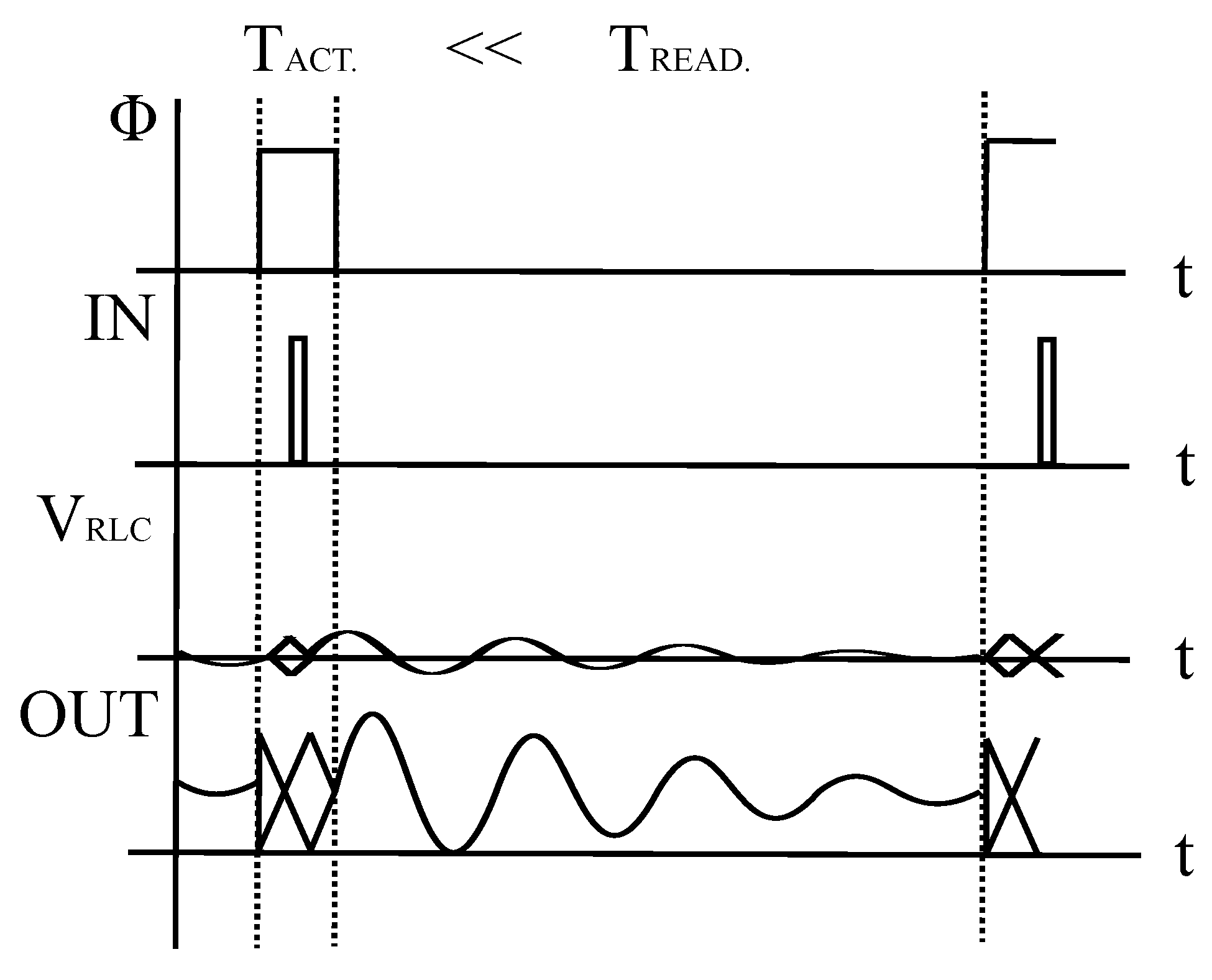
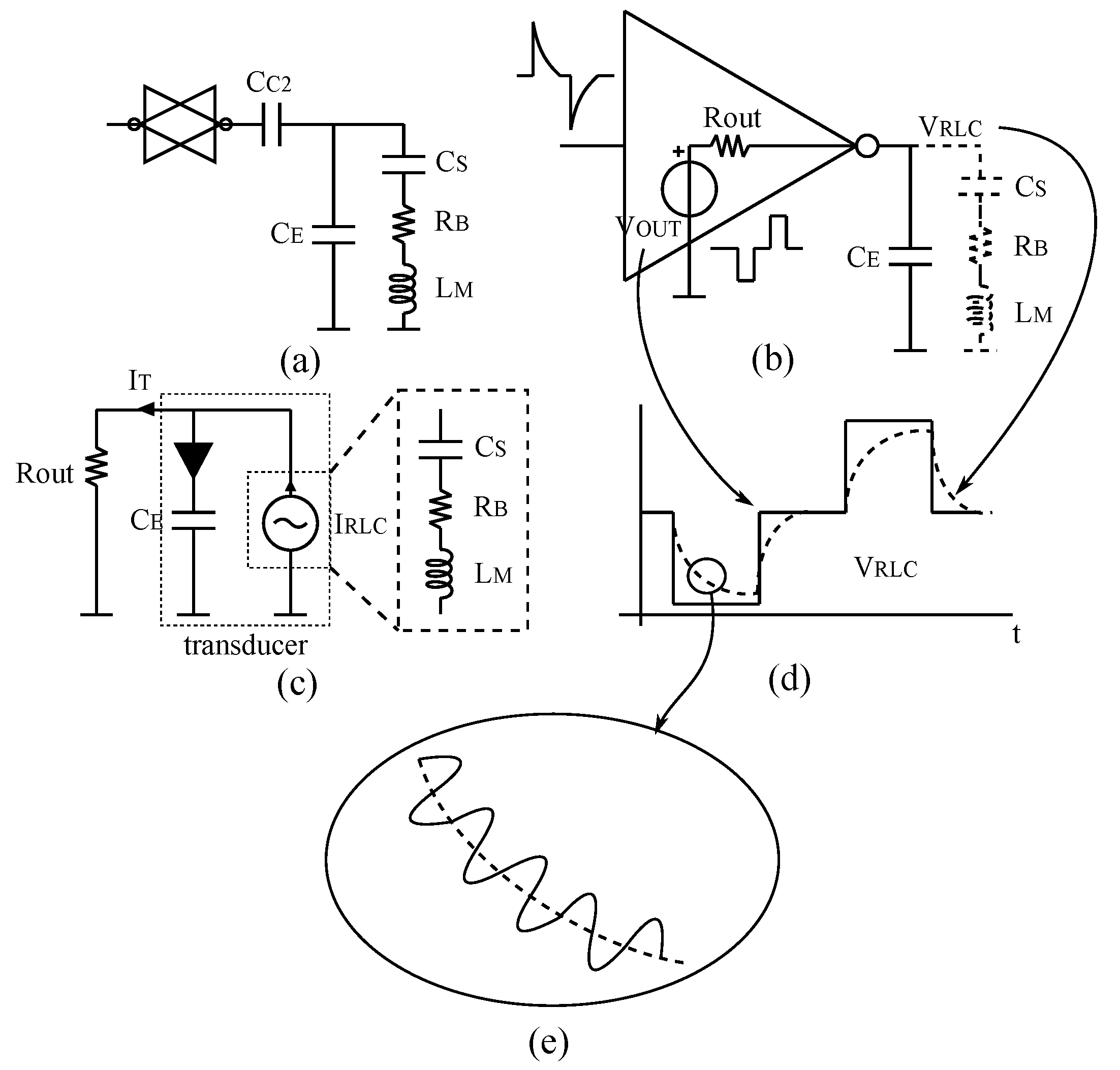
9] mainly due the control system necessary to track the resonant frequency. Therefore, in this paper the third method will be applied to read-out the sensor. Typically, the measurement set-up for this technique requires two different circuits as shown in
Figure 1a.
One is used to excite the sensor (TX) and the other to read the response (RX) but both use an amplifier as the main building block to implement the analogue front-end (
). These two front-ends work alternatively by means of a multiplexer/demultiplexer, which addresses correctly the flow of the signals. The sensor response read at the output terminal of the front-end consists in a sinusoidal oscillation, which decays exponentially due to the mechanical damping. It contains two types of information about the resonant sensor, i.e., the resonant frequency and the quality factor, the last one can be extracted by using a curve fitting method. The frequency of the output signal can be precisely measured by detecting, for example, the zero crossing points, which is usually performed by a digital system [
10]. Thus, the output signal of the resonant sensor is often referred to as “quasi-digital”, which can be interpreted directly by digital electronics without the use of an analogue to digital (A/D) converter [
11]. Due to the intrinsic digital nature of the output waveform, these types of sensors are suitable to realize precise control systems characterized by high reliability, low error rates and low susceptibility to the external interferences and noise [
12]. Even though the information about the measurand is typically extracted from the resonant frequency of the output signal, the amplitude and the phase can be also used to carry information about the physical quantity under measurement in particular applications [
13]. Nowadays, the design of electronic circuits used to implement sensor front-end is focused on compactness and low power consumption. In particular, in those applications where resonating sensors are utilized, a possible solution is to implement a bidirectional front-end based on pseudo floating gate amplifier (PFGA). PFGA has been widely applied to implement many and different types of electronic devices such as: multivalued gate (MV) [
14], analog to digital converters [
15], analog circuits such as band pass filters [
16,
17,
18,
19], tunable filters controlled with bulk voltages [
20], tunable dual-band pass filters [
21], filters based on current-starved PFGA [
22,
23], reconfigurable analogue circuits [
24], to implement mixer and extractor [
25], multiplexer/demultiplexer [
26]. Furthermore, the bidirectionality of PFGA have been introduced in [
19,
24,
25,
26,
27,
28], but never deeply investigated. The first time the PFGA had been thought of as driver for resonant circuits was in Azadmehr et al. [
27]. Such a system was simulated and proved to be, at least theoretically, a valid solution for the purpose. Later on, a prototype was developed to verify the concept with a resistance,inductance,capacitance (RLC) load [
29] and a real piezoelectric sensor [
30]. The aim of this paper consists of providing the design rules of the proposed front-end, which allow for optimizing this type of amplifier for driving and read-out resonating sensors.
The paper is organized as follows:
Section 2 describes the basic concept used to extract a model of a resonating sensor. In
Section 3, it is explained how to use PFGA to implement a bidirectional amplifier. In
Section 4, the analysis and modelling of the bidirectional front-end is provided.
Section 5 provides simulations results to verify the validity of the modelling discussed in the previous section and the design rules.
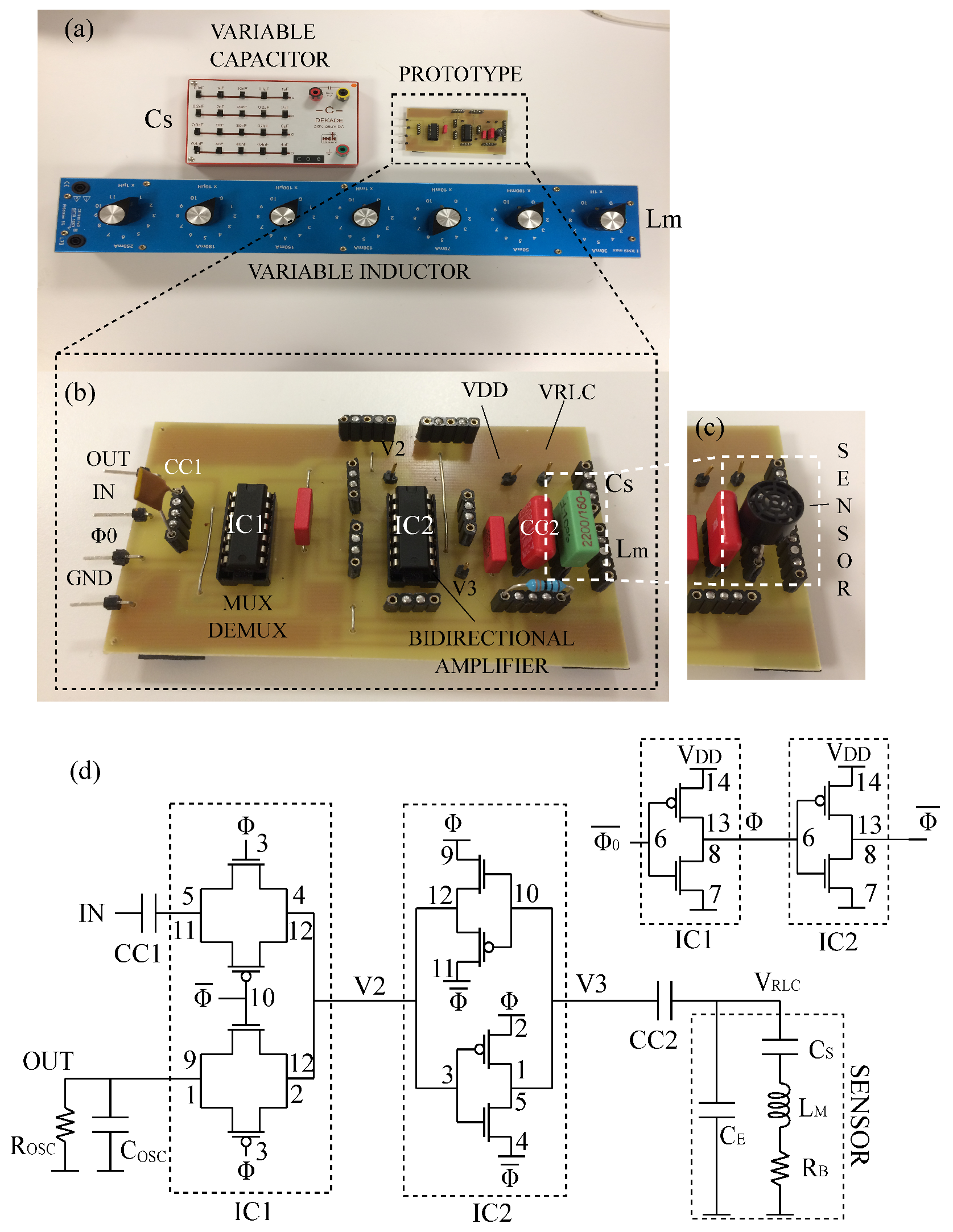
Section 6 describes the measurement set-up used to perform the measurements.
Section 7 presents the measurement results of the tests performed on the prototype. The paper terminates with the conclusions in
Section 8.
3. Bidirectional Amplifier Based on PFGA
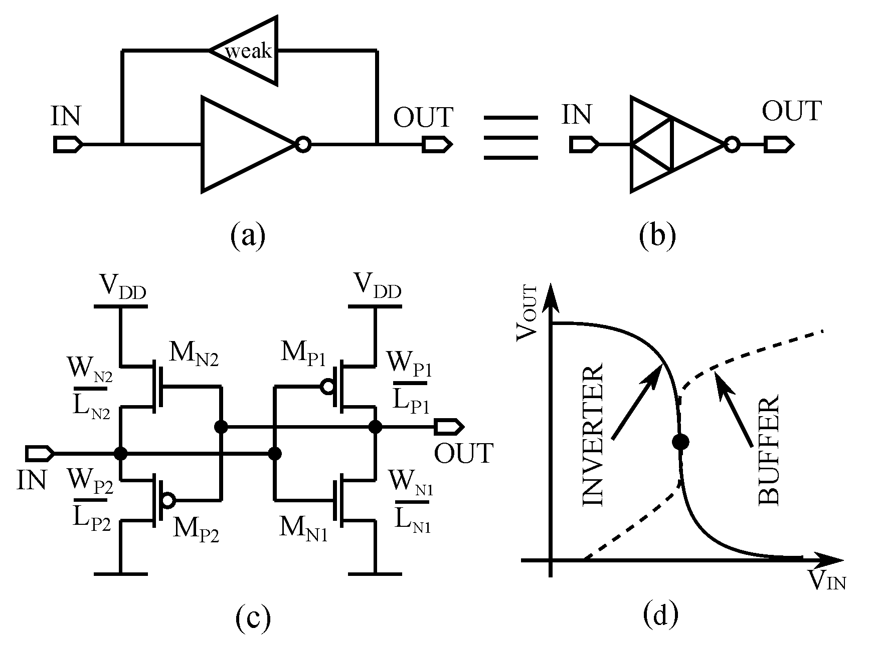
The Pseudo Floating gate Amplifier (PFGA) represented in
Figure 3 is the building block of the proposed bidirectional front-end. It provides compactness and possibility of low power circuits implementation because of the small number of transistors. [
20] provides a detailed description of the basic principle of the PFGA.
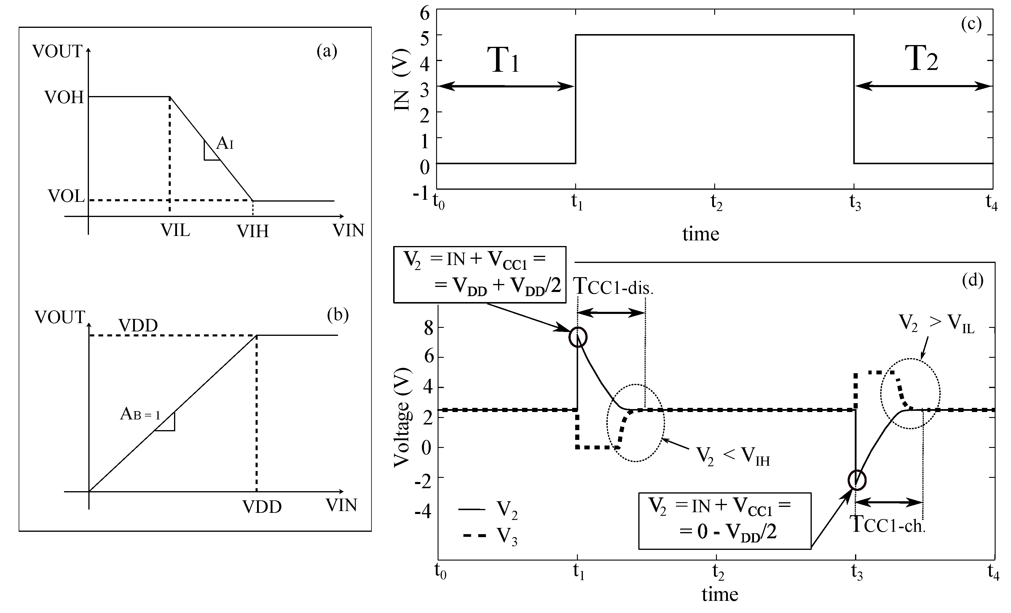
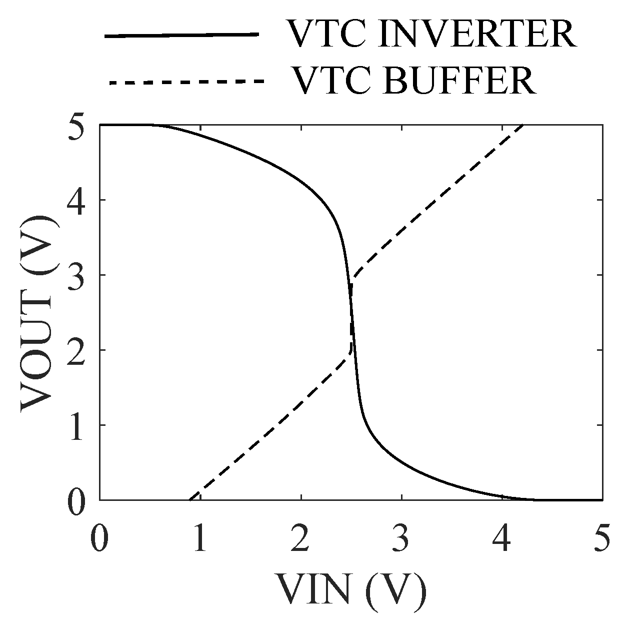
The PFGA is composed of a logic inverter closed in a negative feedback loop with a voltage buffer, which realizes the bias network of the inverter. The steady state of the PFGA is achieved, when both the inverter and the voltage buffer are in equilibrium. This situation can be graphically represented as the intersection of the voltage transfer characteristic curves of the inverter and the voltage buffer, as shown in
Figure 3d, and it occurs ideally when
. The PFGA presents a band pass behaviour, where the low cut-off frequency depends on the capacitance at the input node and the output resistance of the voltage buffer, while the high cut-off frequency depends on the output resistance of the inverter and the load capacitance. Therefore, the design of these two elements set the bandwidth of the whole amplifier. Secondary effects such as offset, leakages and nonlinearities have been already discussed in literature, but they will be re-mentioned during this work to emphasize their effects in this application. The PFGA presents a small transconductance inherited by the logic inverter inside this structure, which lowers the gain of the amplifier. Nevertheless, the sensitivity of the amplifier can be increased by cascading more than one PFGA. This type of amplifier has already been proved to be functional if implemented in high leakage CMOS (Complementary metal oxide semiconductor) technologies because the biasing of the inverter is based on the channel leakages of the voltage buffer. However, an implementation in low leakage processes introduces new challenges. The most important is the inability of the system to reach the equilibrium state because the leakage currents are too low to drive the feedback reaction and bring back the system to the ideal state in a reasonable time. A simple representation of this problem is shown in
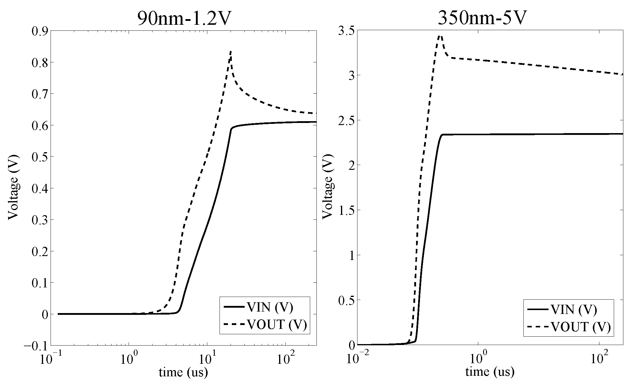
Figure 4.
Figure 4 compares the transient time to reach the equilibrium state of two PFGA, one implemented in high leakage CMOS process Predictive Technology Model (PTM-90nm) and the other one in low leakage CMOS process (Austria Mikro Systeme AMS-350nm). It can be observed that the high leakage PFGA does not take a long time to approach
V, while the low leakage PFGA takes a much longer transient time before it reaches the equilibrium state. This characteristic would be already sufficient to limit the implementation of the bidirectional amplifier to high leakage CMOS processes; however, in this paper, it will be proved that, thanks to the working operation of this front-end, low leakage technologies are also suitable to realize this device.
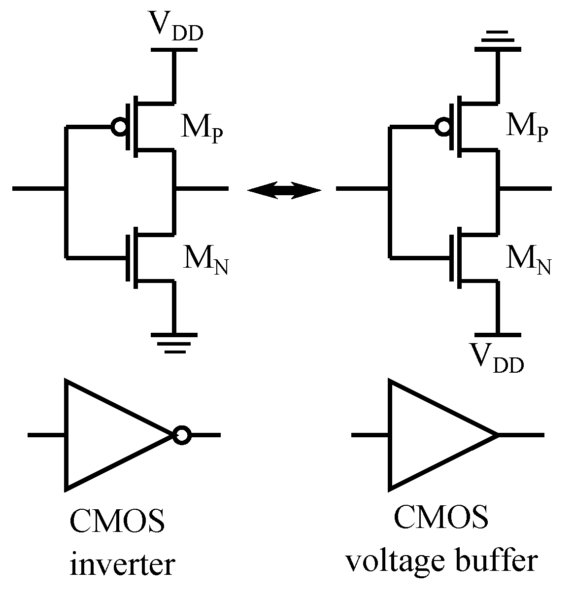
The bidirectionality of the PFGA is achieved by swapping the rails of the power supply. Indeed, the CMOS inverter and the CMOS voltage buffer in the PFGA present a sort of symmetry, which is highlighted in
Figure 5.
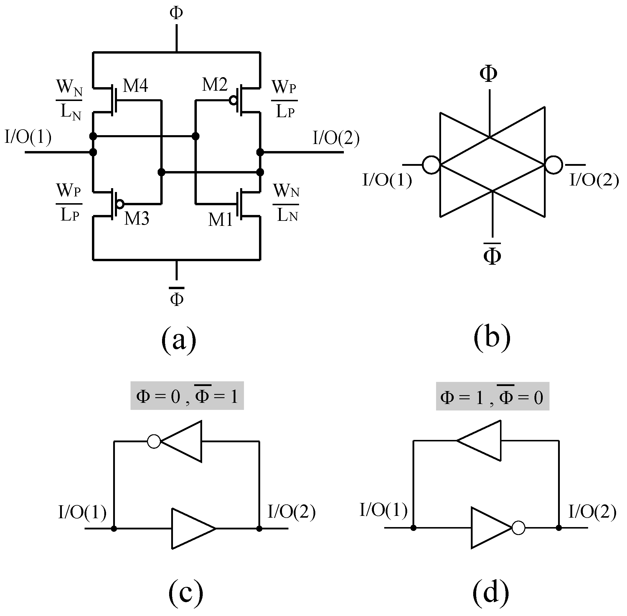
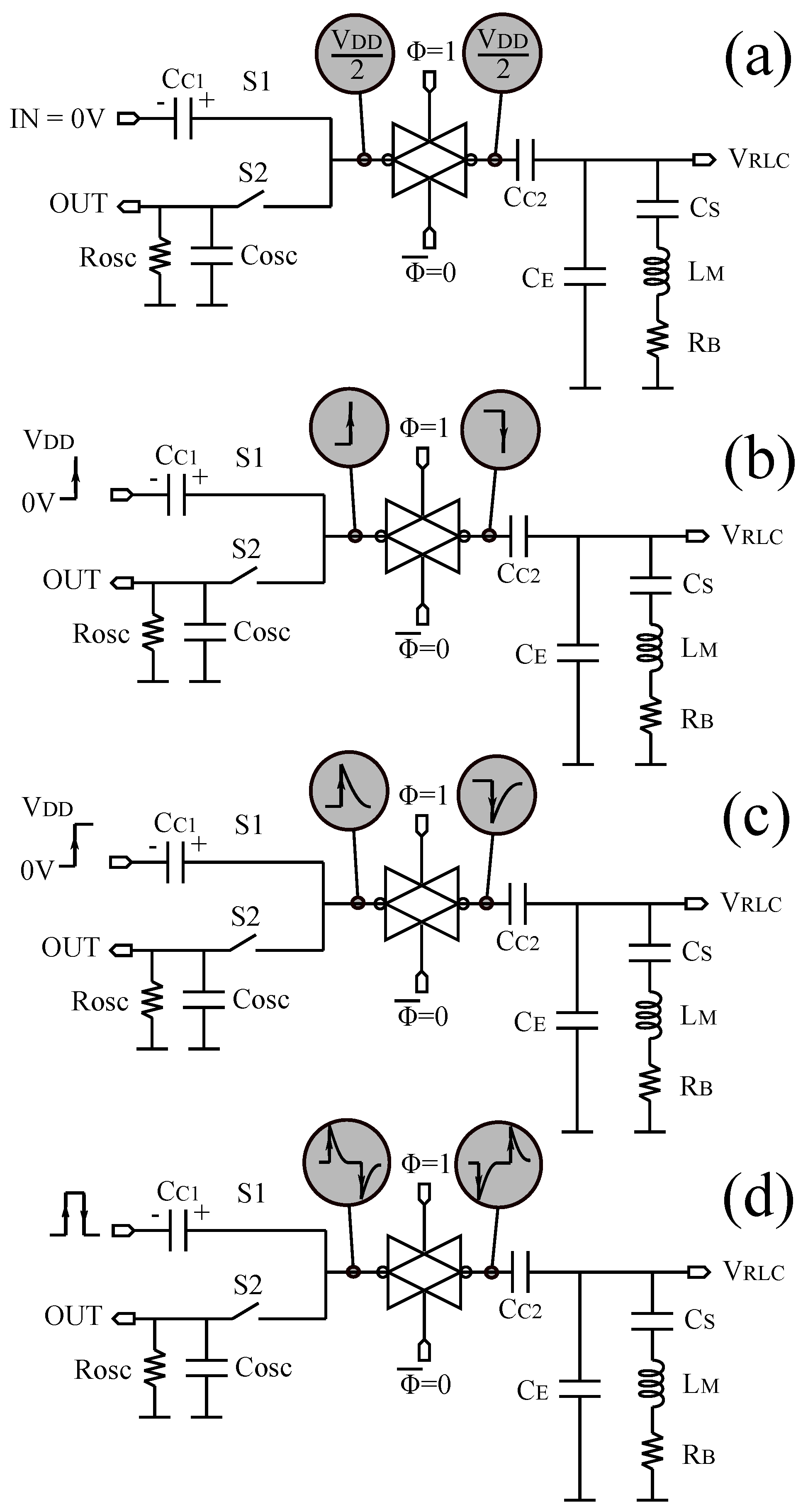
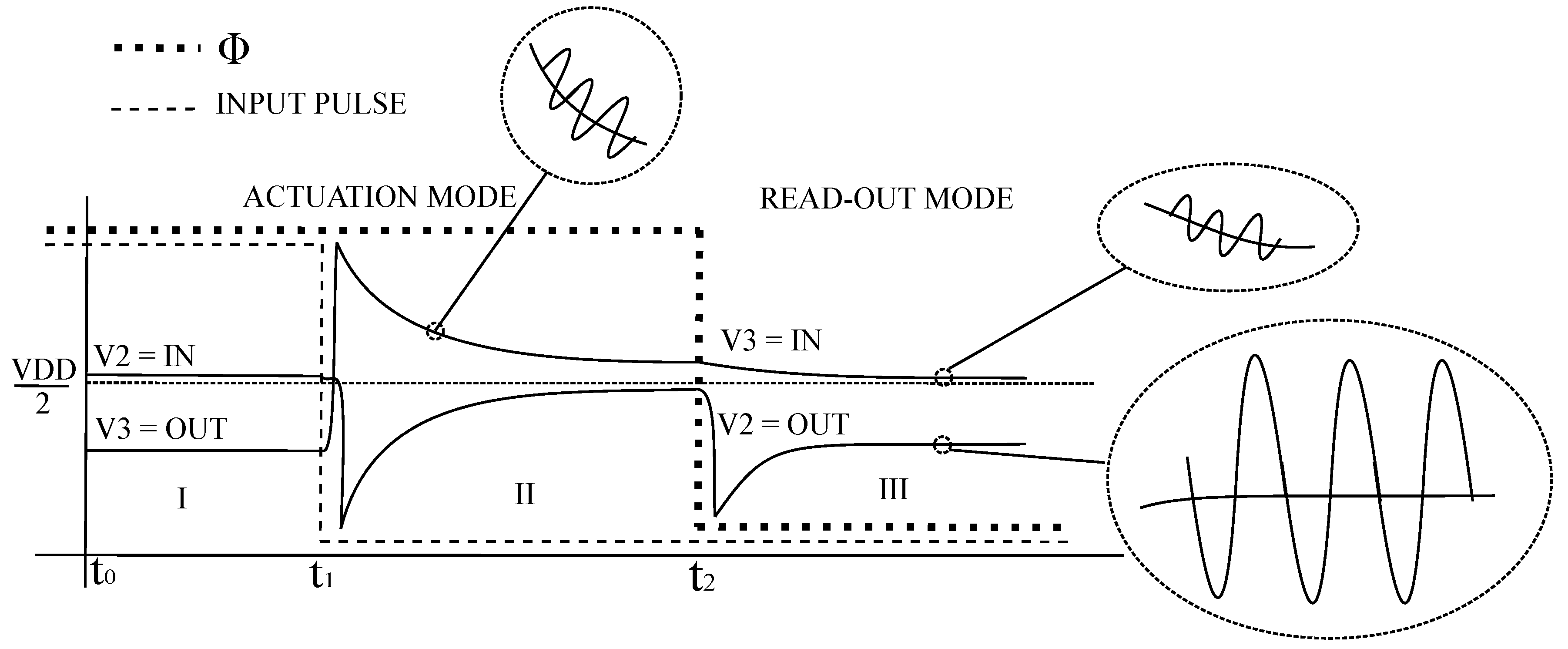
The working principle of the bidirectional amplifier has been represented in
Figure 6 and can be summarized as follows. The power supply of the PFGA is now considered a control signal and indicated with
and
. Signals can flow from I/O(1) to I/O(2) when
VDD and
GND, and vice versa, signals flow from port I/O(2) to port I/O(1) when
GND and
VDD as shown in
Figure 6c,d. From an ideal point of view, the bidirectional amplifier can be considered as a normal PFGA, which mirrors or flips when the power supply rails are swapped.
The symbol adopted for this circuit shown in
Figure 6b follows by the fact that the amplifier is implemented by a logic inverter, which reverses its direction. At transistor level , it is possible to recognize that if
,
then M1 and M2 realize the inverter while M3 and M4 the buffer. If
,
, then M1 and M2 realize the buffer while M3 and M4 the inverter. The bidirectional amplifier obtained is compact, made only by four transistors, which implies a small occupation of area on the chip and potentially lower power dissipation.
5. Simulation Results and Design Rules
Simulations by using a low voltage (LV) model nmos4/pmos4 in AMS-350nm technology at
V has been used to support the modelling previously discussed and to perform a quantitative analysis useful to define design rules for this front-end. It must be noticed that the main results are also valid for high voltage models and high leakage implementations. The dimensions of the MOSFET used in the simulations are listed in
Table 1.
First of all, the voltage characteristics curves of the PFGA utilized to implement the bidirectional amplifier are shown. These curves are shown in
Figure 16.
Figure 16 shows an inverter with a linear region approximately in the range of [1.5 V, 3.5 V] and a voltage buffer characterized by an OFF (output voltage range in which the buffer is turned OFF) region in the range [1.8 V, 3 V]. In literature, it has been proved that this PFGA cannot work if implemented in low leakage CMOS processes because the small magnitude of the leakage currents doesn’t allow the amplifier to reach the equilibrium point. This phenomenon is exploited in the simulation shown in
Figure 17.
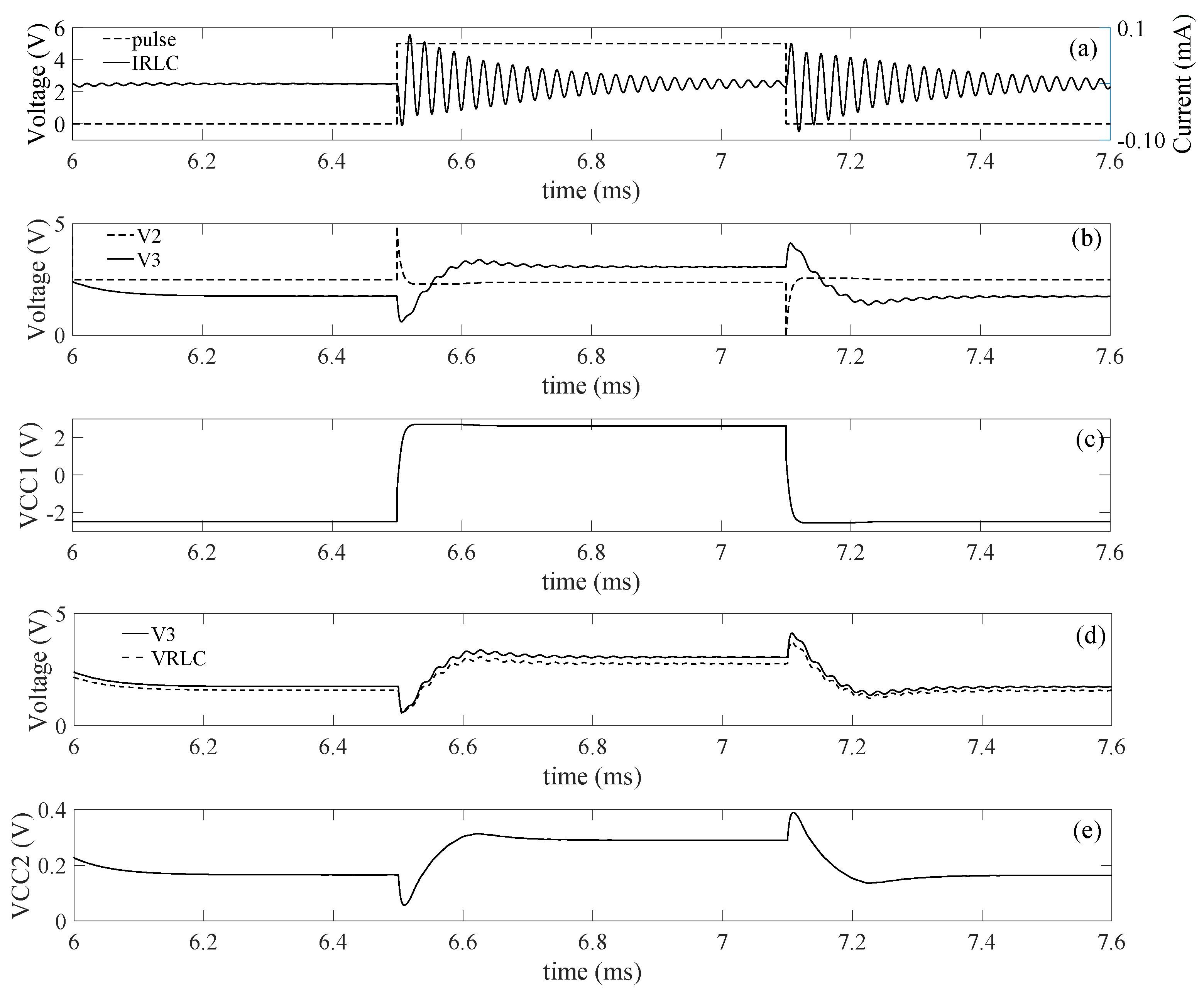
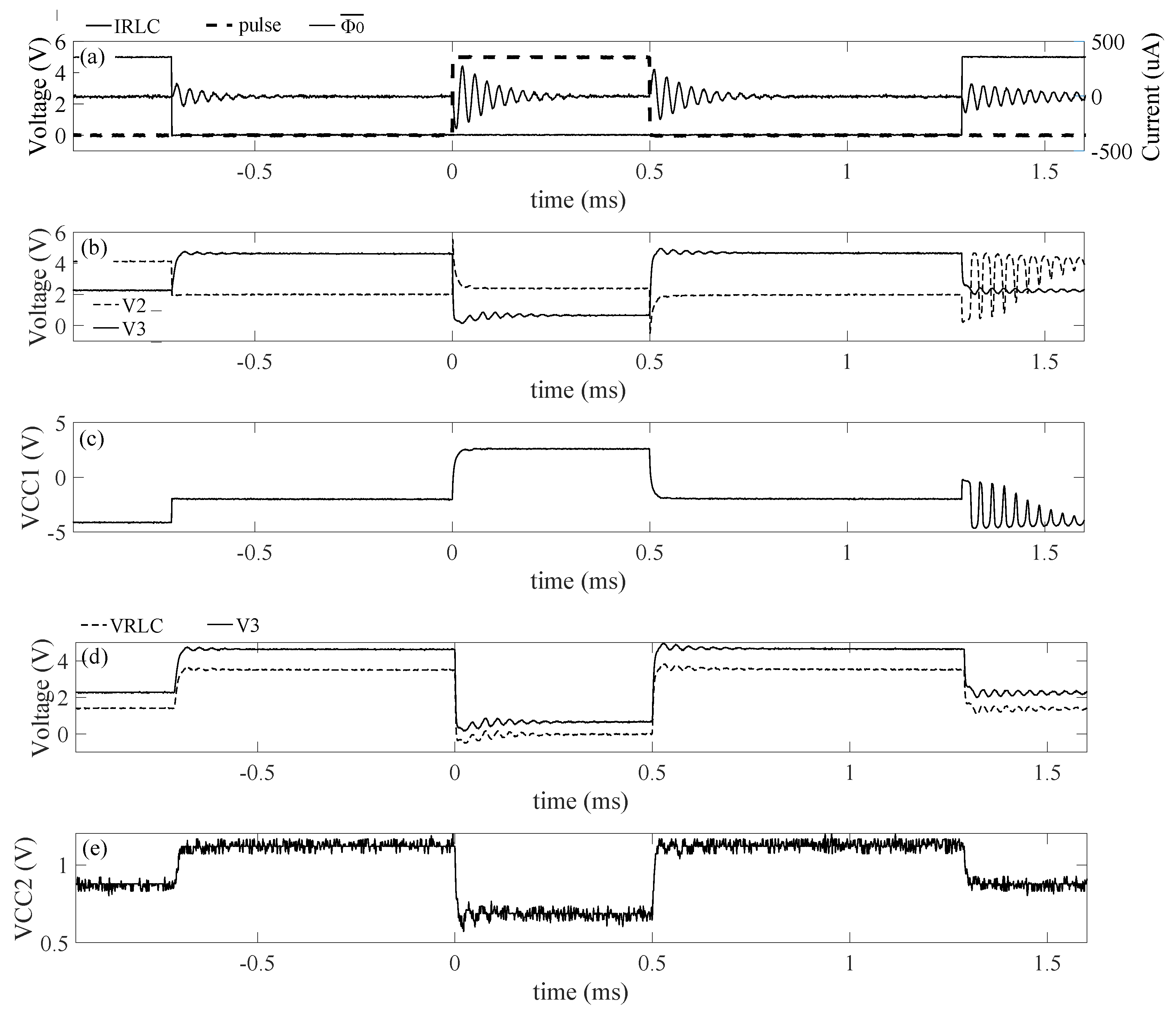
Figure 17 shows the waveforms of the signals in the bidirectional front-end during the actuation mode. In
Figure 17b, it can be observed that the steady state value of the input and the output voltage of the bidirectional amplifier are never equal. This is the result of the input offset of the PFGA. The input signal of the bidirectional amplifier assumes the same shape predicted by the theoretical model, while
does not reach the power supply rails. This is due to the very fast dynamic of
, which approaches the steady state value faster than
. Another expected phenomenon is the double excitation of the resonating sensor as shown in
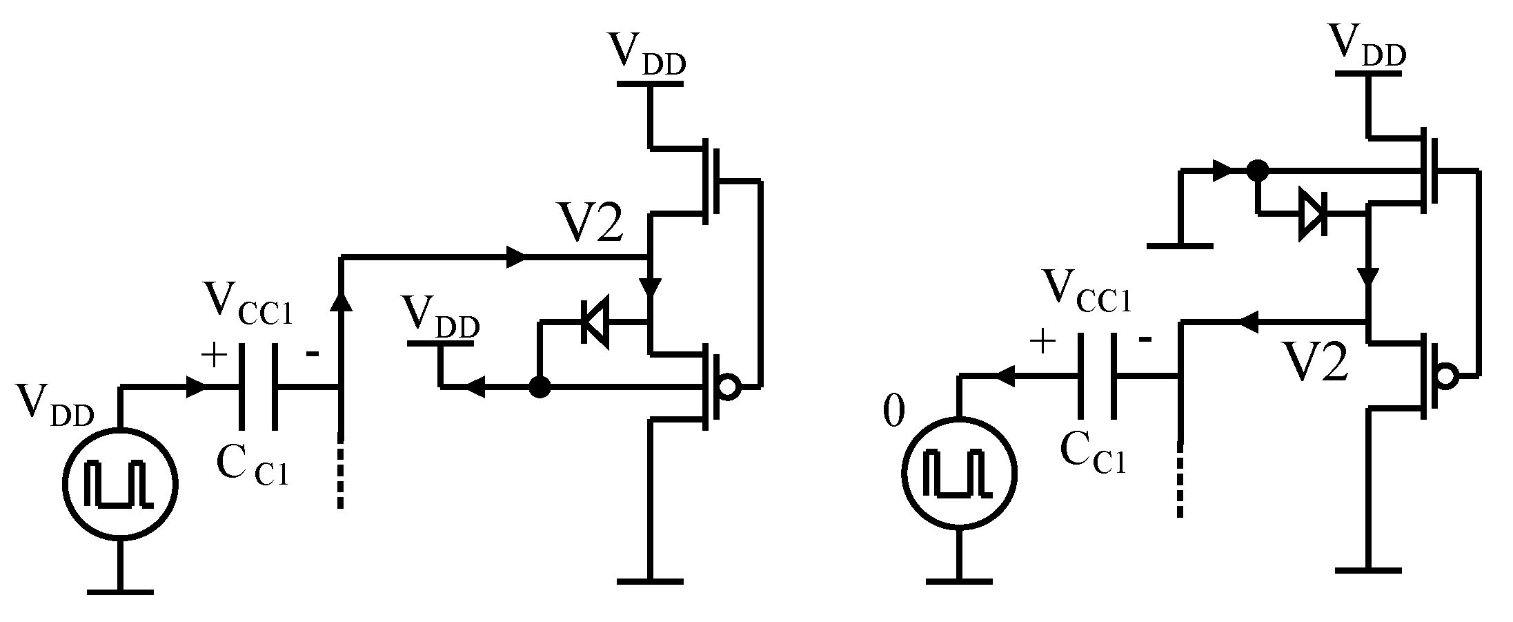
Figure 17a. In this case,
always assumes values inside the power supply range, which means that the body diodes shown in
Figure 11 are not turned on. This is because the MOSFET (M3, M4) provide a fast feedback reaction, which impede
from reaching the power supply rails.
Figure 17c shows the voltage across the input coupling capacitor
changing between two opposite values. This is due to the fact that the equilibrium in the system is kept by charging and discharging this capacitor.
Figure 17d shows that the voltage
and
are not equal as expected, but they keep a constant distance between each other. Indeed,
is not infinite and therefore the voltage across this capacitor is given by the voltage divider formulas in Equation (
2):
In this particular scenario,
= 22 nF,
= 2 nF,
= 300 pF, which means that
is characterized by an average voltage around 1/11 times the steady state value of
, as proved by the signal shown in
Figure 17e.
Figure 17a shows a small oscillation at the very beginning of the actuation mode, which is induced by the transition from actuation to read-out mode as described in the previous section.
Figure 17b shows that this transition produces a variation in
, which is probably the cause of the unwanted oscillation. Finally, it can be noted that a small oscillation is overlapping the signal
after the rising edge of the input pulse, which is due to the contribution of the RLC series elements to the dynamic of the circuit as described in
Figure 12e.
The analysis of these waveforms can be used to extract design rules for this electronic circuit. First of all, the main excitation of the resonating sensor, represented by the current
, is the one provided by the falling edge of the input pulse because it is the last one that excites the transducer. However, the amplitude of this oscillation depends on the value of the current
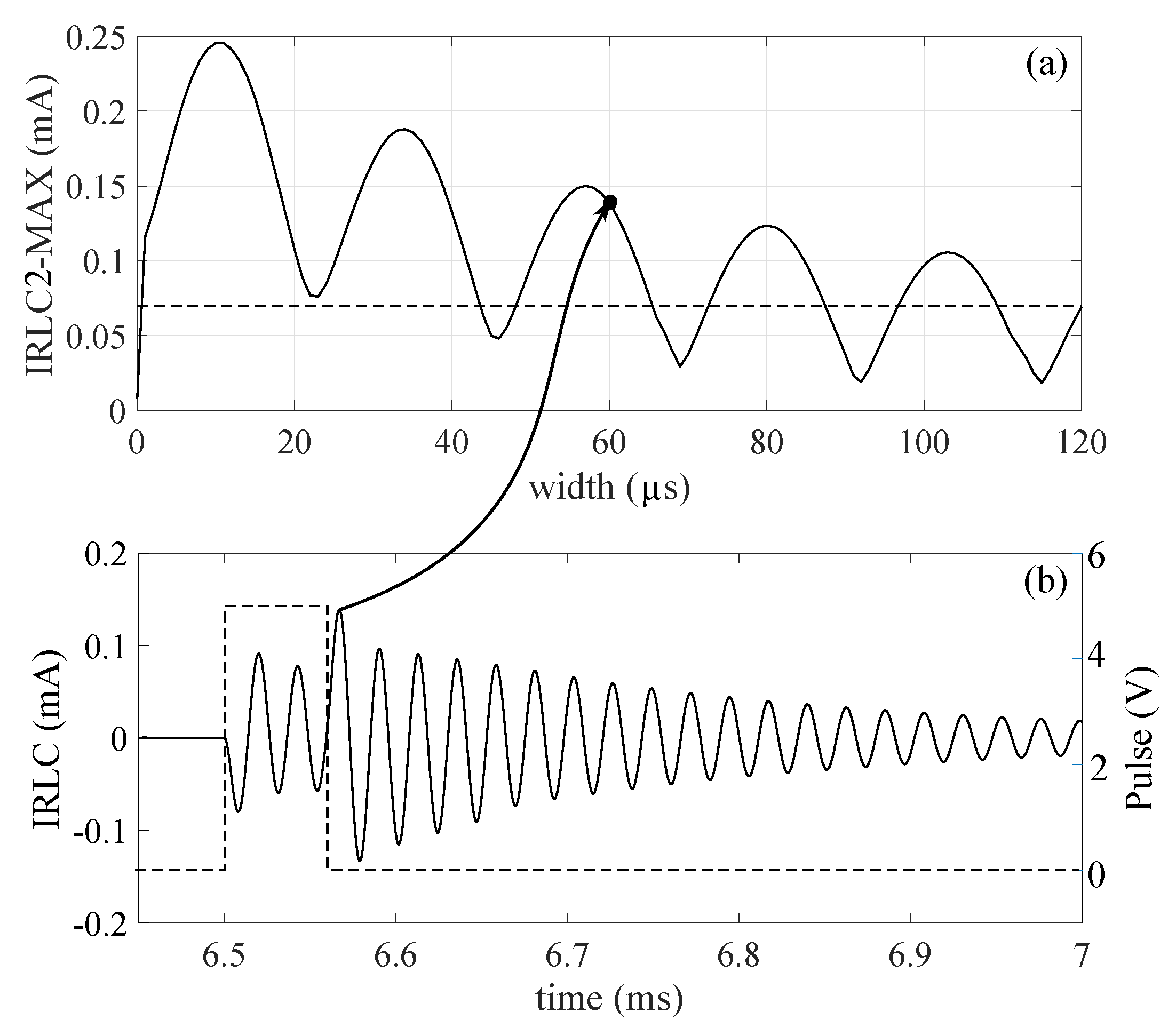
at the occurrence of the falling edge of the input pulse. In particular, it depends on the fact if the oscillation generated by the rising edge of the input pulse is already completely damped or is still going on when the transducer is excited the second time. The possibility to wait the complete damping of the first oscillation to start the second one must be discarded because it limits the performance of the circuit. In this case, the width of the input pulse would be equal to the damping time of the oscillation generated by the sensor, which can be very long, reducing the time available for the read-out mode. Therefore, the interaction between the first and the second oscillation must be accepted, in order to provide reasonable timing for the signals in the circuit. Next, a test has been performed to research the optimum value of the width of the input pulse, which provides the maximum excitation to the transducer. The simulation results are shown in
Figure 18.
The input pulse width is swept in a range [1
s, 120
s] and, for each test, the first positive peak of the oscillation induced by the falling edge of the input pulse has been recorded as shown in
Figure 18b. These values have been collected in a curve called
as shown in
Figure 18a.
Figure 18a shows that the maximum value of this curve is about 3.5 times the value that it would assume if the falling edge is applied after that the first oscillation is completely damped (dashed line). This value is considered as a reference for the minimum
amplitude acceptable. There do exist some values of the input pulse width that reduce the amplitude of the oscillation, with respect to the reference value. On the other hand, there does also exist a range of values in which any value of the width will provide a greater or equal amplitude than the reference value (in this case width ≤ 44
s ). This range will be referred in this paper as the “safe range” for the value of the width of the input pulse. A list of the local maximum of the
curve is shown in
Table 2.
Table 2 shows that the local maximum occurs with the same period of the resonant oscillation as expected (
= 23
s,
= 43.4 kHz). In particular, the absolute maximum is found for a pulse width of 10.5
s, which is almost
. In conclusion, the width of the input pulse must be tuned around
, in order to obtain the maximum excitation of the sensor, where
is the period of the oscillation generated by the resonating load. Nevertheless, during the normal operation of this front-end, the resonant frequency can change its value due to variations of the measurand or due to unwanted phenomena, and it can affect the efficiency of this technique. By the way, in both cases, the variation of the resonant frequency is usually just a small percentage of the nominal value, so it doesn’t have a relevant effect on the dynamic of the system.
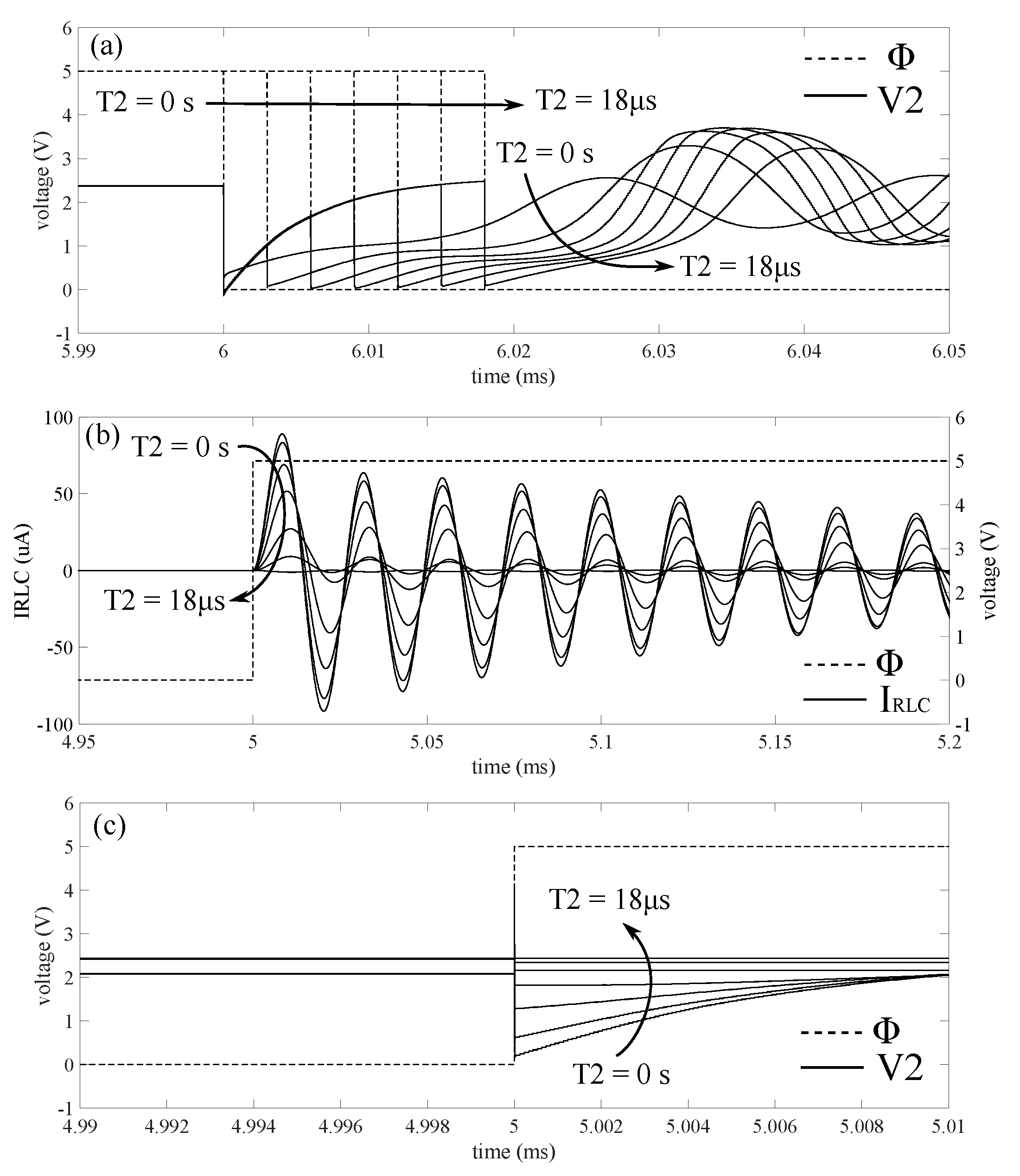
Next, the transition read-out mode to the actuation mode was studied. The simulation results are shown in
Figure 19.
Figure 19b shows that this transition brings the transducer to oscillate, as supposed during the modelling. The origin of this oscillation has been investigated by performing a simulation where the transition actuation mode to read-out mode has been delayed of a time interval
swept in a range [0
s, 18
s]. As predicted by the modelling provided in the previous section, if the signal
approaches
before passing to read-out mode, then the oscillation generated at the beginning of the actuation mode reduces its amplitude. This analysis provides the missing parameter for the estimation of
or the duration of the actuation mode, which can be expressed as shown in Equation (
3):
where
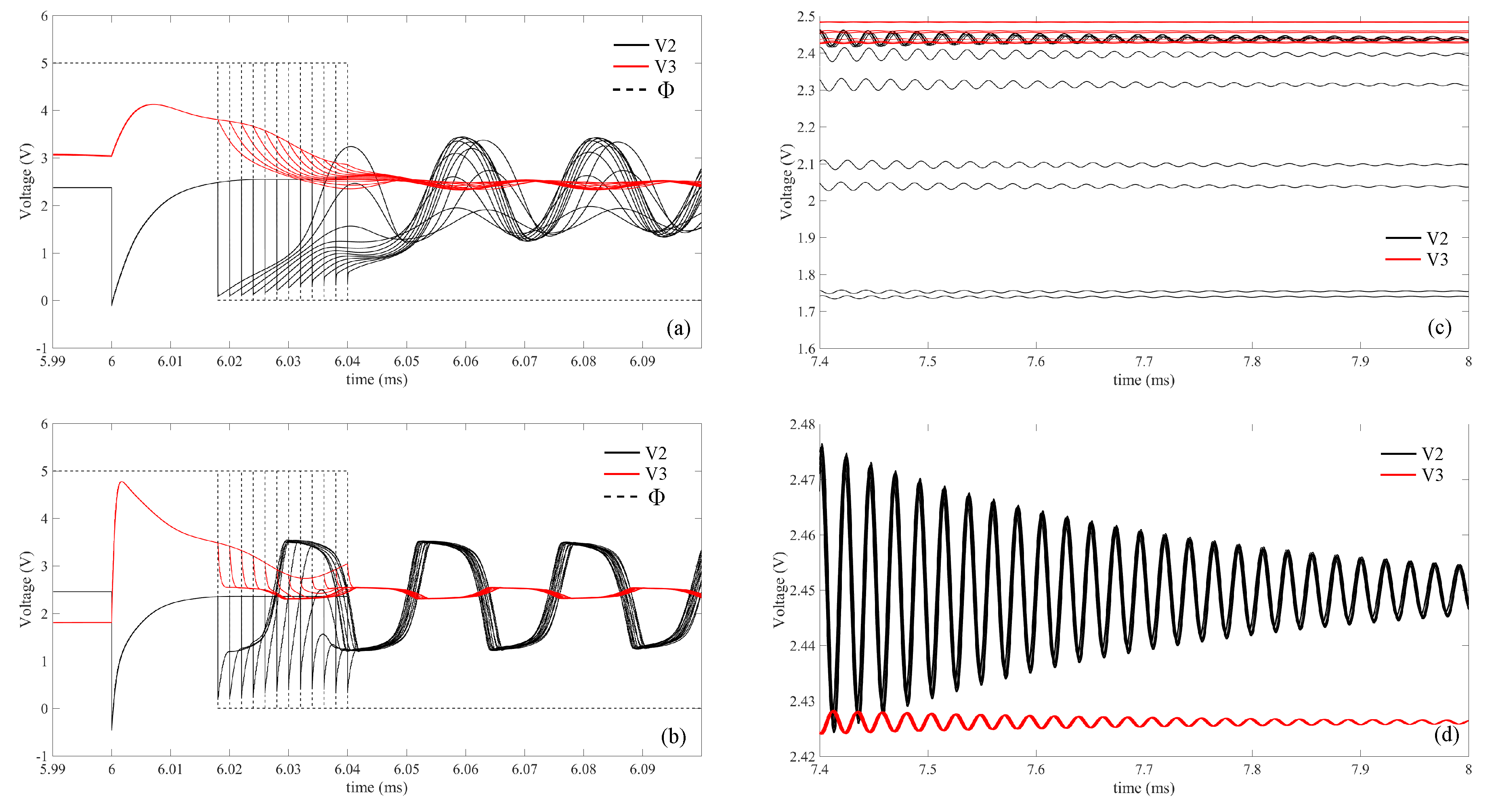
is an arbitrary value. Next, the effects of the transition actuation mode to the read-out mode depend on the duration of the actuation mode duration were analyzed. The simulation results are shown in
Figure 20.
A simulation has been performed by sweeping the time interval
in the range [18
s, 40
s].
Figure 20a shows the waveforms of
and
a few instants after the transition from actuation mode to read-out mode, while
Figure 20c shows the same waveforms after the oscillations are almost completely damped. The results in
Figure 20a,c show dispersive waveforms with different steady state values depending on the value of
. The main cause of this dependency is supposed to be due to the shape of
after the transition. Indeed,
approaches the steady state value exponentially and it requires different times. Furthermore, while
decreases, the oscillation generated by the transducer overlaps the main signal affecting the shape of
. The combined effect of these two causes provides different steady state values. The first contribution can be reduced by increasing the rate at which
approaches to the steady state value. This can be achieved by increasing the size of M1, M2. Another simulation has been performed by increasing of ten times the size of M1, M2 (
= 10
m/350 nm,
= 23
m/350 nm). The simulation results are shown in
Figure 20b,d. As expected, the waveforms provide more regular behaviour, but, most important, they are characterized by the same steady state value. In conclusion, it has been proved that the transition from actuation mode to read-out mode is affected by the duration of the actuation mode. In particular, the position of the bias point is strictly related to the dynamic behaviour of
. Finally, it has been proved that the stability of the bias point in read-out mode can be improved by using stronger MOSFET M1 and M2.
Another constraint does exist, which can be extracted from this simulation. If the bidirectional front-end is implemented with high threshold voltage transistors (low leakage process), then the threshold voltage of M2 must be: . If this condition is not satisfied, the input voltage cannot approach close enough to and the performance of the bidirectional amplifier will degrade.
Finally, the analysis of the read-out mode can be performed by using the results in
Figure 20. The oscillation
generated by the transducer during the read-out mode presents a sinusoidal shape in
Figure 20a, while it is distorted in
Figure 20b. The cause of this distortion is the voltage buffer inside the PFGA, which, once turned on, “clamps” the input and consequently the output signal of the amplifier. The voltage buffer turns on only for the case (b,d), because the wider amplitude of the signals
during the read-out mode. This is mainly a consequence of using a strong inverter during the actuation mode for the case (b,c). A strong inverter provides a greater excitation of the transducer for the case represented in
Figure 20b than the case in
Figure 20a (observe
(t = 6 ms)). Furthermore, it provides a more stable bias point as shown in
Figure 20d than the case shown in
Figure 20c, which is due to the lower output resistance of the amplifier. Therefore, the position of the bias point in
Figure 20d is closer to the ideal value than the case shown in
Figure 20c maximizing the gain of the amplifier. Finally, the combination of these two contributions provides a wider amplitude of the input and the output signals, which turns on the voltage buffer and introduces nonlinearities in the circuit.
The simulation results of the read-out mode has been used to describe the distortion phenomenon presented in the output signal , discussing the origin of this phenomenon.
In conclusion, simulation results show that the bidirectional amplifier will work if implemented in both high leakage and low leakage technologies, even though the last one has been proved in literature to not be suitable to implement a standalone PFGA without compensating the offset. An implementation in low leakage technology requires a few more design considerations than the case of a high leakage implementation, but the system is still functional.
5.1. Design Rules
The theoretical modelling and the simulation results provided a deep understanding of the working principle and the secondary phenomena, which take place in the proposed front-end. These results have been collected in this section in order to provide a step-by step procedure to design this device by running a few simulations.
First of all, the following steps will be performed by using a BvD load. Second, the inverter of the bidirectional PFGA must be designed in order to provide the gain, the bandwidth and the output current needed for the application. Once the inverter dimensions are set, the same aspect ratio for the MOSFET of the voltage buffer can be chosen. This will provide the same strength for the feedback and the amplifier. The value of
can be set initially to 10 times of
. This parameter is usually reported in the datasheet or can be extracted by the BvD model of this device. The initial value for
is arbitrary because it will be tuned in a next step. A test with very wide input pulse duration and actuation mode must be run as shown in
Figure 17. It is now possible to tune
to allow the peaks in
to reach the rails of the power supply and maximized the excitation provided to the sensor. Then, the time
must be recorded because it will be used to set the duration of the actuation mode. A this point, by measuring the peaks of the signal
, it is possible to recognize if the source-bulk pn junctions of the MOSFET in the voltage buffer turn on. If these diodes turn on the size of M3, M4 must be increased to reduce the risk of latch up phenomenon. Next, the duration of the input pulse can be set around half of the oscillation period generated by the transducer. Monitoring the current
will help to tune more precisely the duration of the input pulse. Once the excitation of the transducer is maximized, it is possible to fix the duration of the actuation mode by using the value
previously recorded. The duration of the actuation mode can be fixed according the formulas in Equation (
3). Finally, a sweep in the duration of the the actuation mode must be performed to check if the bias point of the amplifier is affected by the transition from actuation mode to read-out mode. If the oscillation is influenced by the value of
, the dimensions of the MOSFET M1, M2 must be increased until the dynamic of
becomes independent from the value of
. This will improve the immunity of the system to the variations of the actuation mode duration. In conclusion, by using these simple steps, it is possible to design the set-up of a bidirectional front-end based on a pseudo floating gate amplifier.
7. Measurement Results
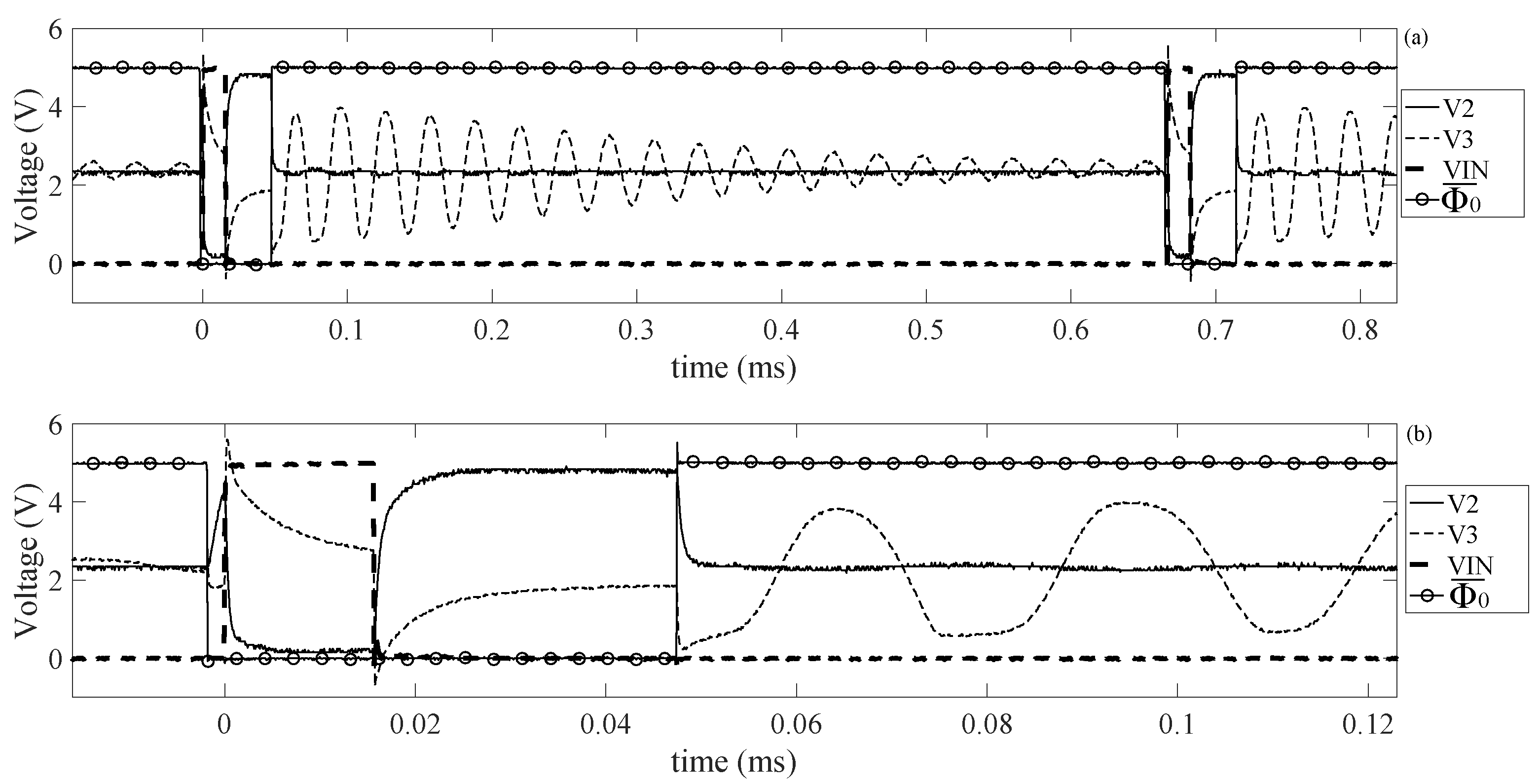
First of all, the signals have been measured during the actuation mode, trying to replicate the simulation results in
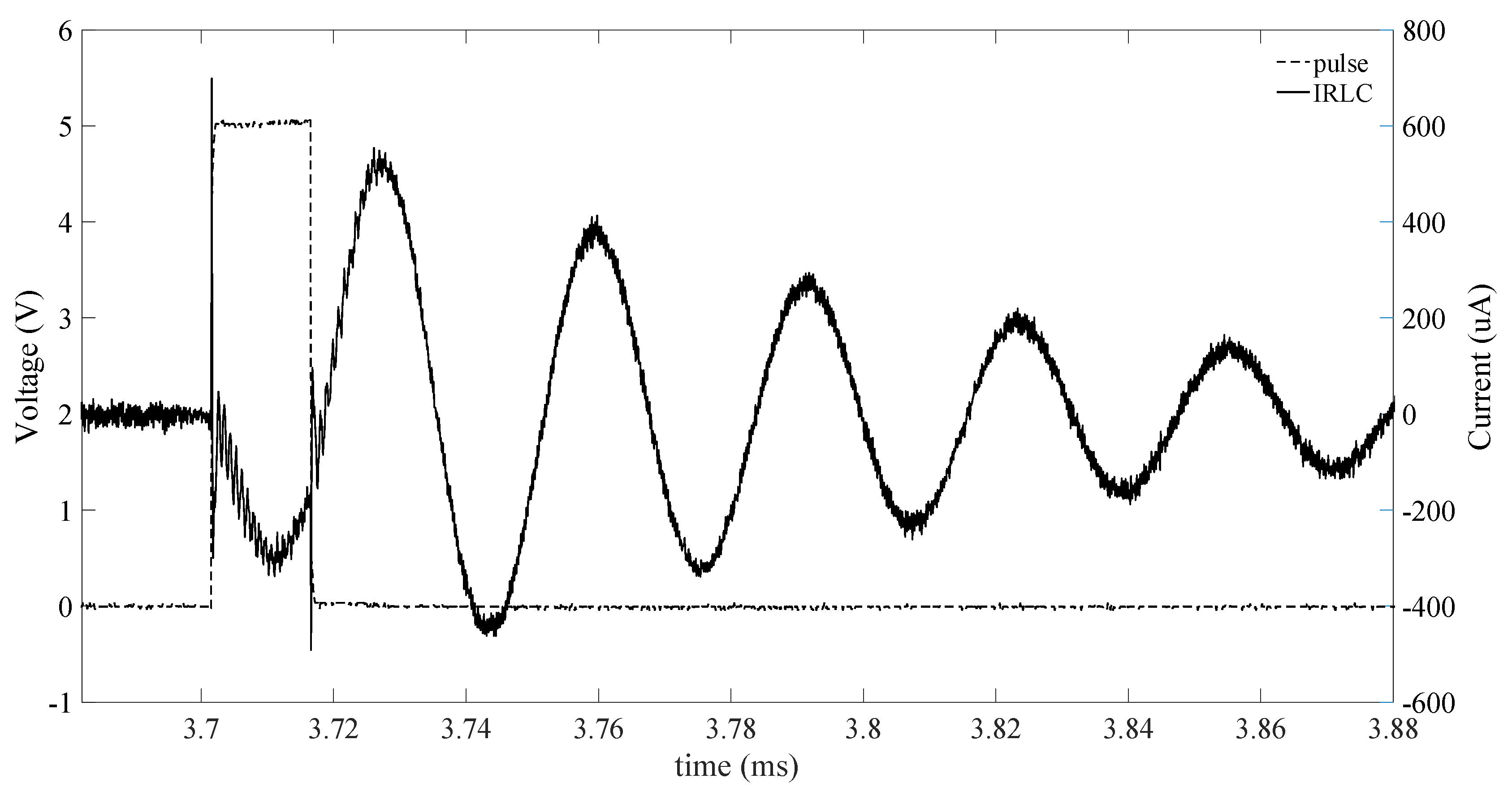
Figure 17 by using a BvD load. Measurement results are shown in
Figure 22.
The waveforms in
Figure 22 show good fitting with the simulation results in
Figure 17, with a few differences. The first one is that the steady state value of
is quite far from the steady state value of
because the implemented voltage buffer is characterized by a wide off region. The oscillation generated by the BvD load is characterized by a frequency of 32.4 kHz, which is smaller than the resonant frequency of the real transducer.
is characterized by a greater drop voltage than the value expected (
V). This is probably due to the fact that the parasitic capacitance in the circuit increases the total capacitance at the node
, which is greater than the only
, modifying the voltage divider between
and
. The duration of the read-out mode has been set in order to allow the complete damping of the sensors response.
Figure 22a shows the presence of an unwanted oscillation after the transition from read-out mode to actuation mode. In order to neglect any effect of this oscillation, the time
has been fixed almost equal to 0. Next, the value for the duty cycle of the input pulse has been set to
(
Hz) as shown in
Figure 23. This value corresponds to 15
s, which is almost half of the oscillating period of the signal generated by the sensor as expected.
The oscillation generated by the falling edge of the input pulse reaches a peak value of 550
A. This value is around 2.5 times the maximum amplitude of the current oscillation
ms) = 220
A in
Figure 22a. Finally,
is fixed to the minimum value, which allows
to charge to the steady state value of
before to pass in read-out mode. At this point, the duration of the actuation mode has been fixed. The frequency of the signals has been adjusted from 200 Hz to 1.5 kHz to minimize the duration of the read-out mode. Therefore, the optimum duty cycle of the input pulse must be adjusted to
. The parameters used for the control signals are:
kHz,
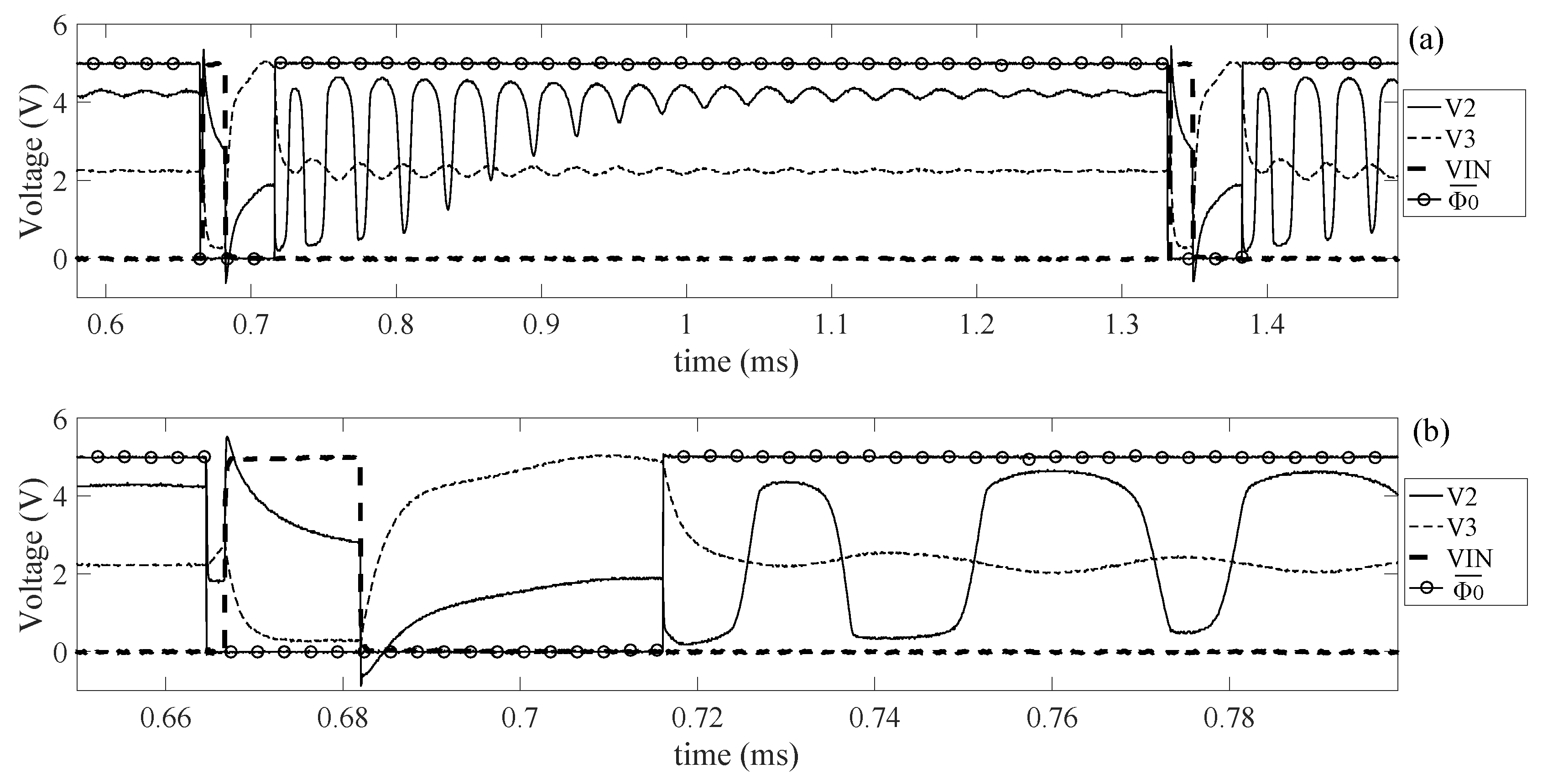
. Measurement results of a whole read-out cycle is shown in
Figure 24.
Measurement results show signals, which fit the predictions of the simulation results. With two main differences: the first one is the fact that
doesn’t show an impulsive waveform, but its shape resembles more the charge and the discharge of a capacitor. The second one is the non ideal positioning of the bias point. This last phenomenon is due to the slow and exponential transient of
when it approaches the steady state value in read-out mode. It is interesting to notice that the peaks at
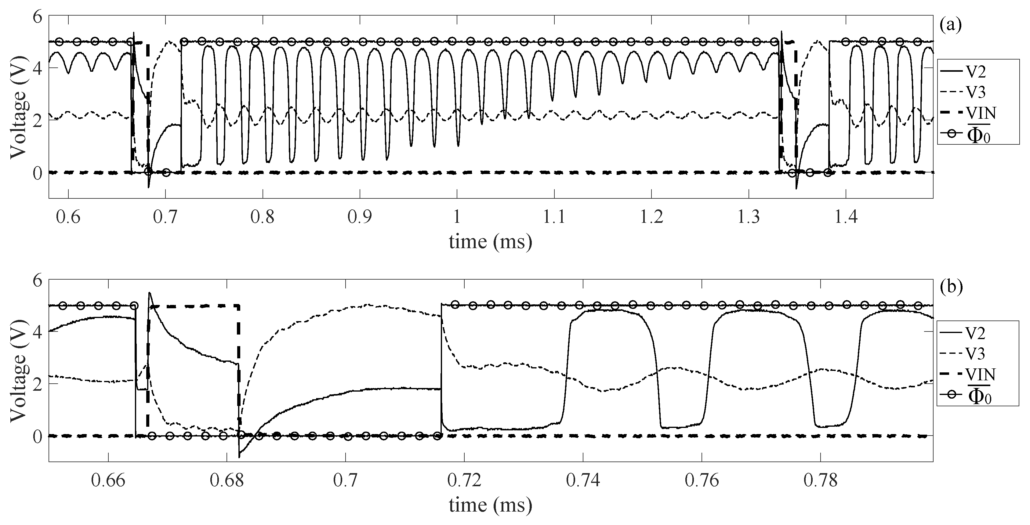
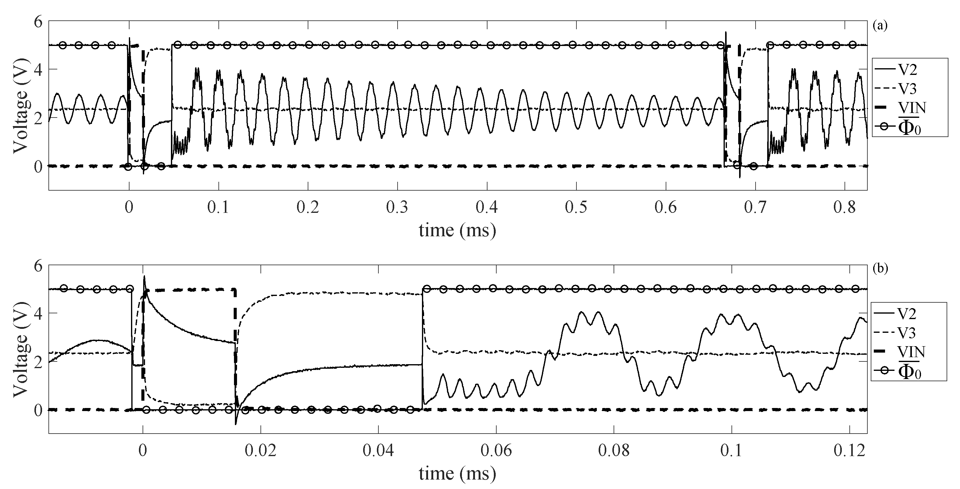
exceed the power supply range reaching the values 5.5 V, −0.88 V. These two values indicate that, in this test, the source-bulk pn junctions of the MOSFET M3, M4 are forward biased. Therefore, greater dimensions for these MOSFET must be used to reduce the risk of latch up. Then, a second test has been performed by using the same parameters for the control signals but using a piezoelectric resonator as load. Measurement results are shown in
Figure 25.
These waveforms are very similar to the one obtained for the BvD load. However, the amplitude of the oscillation of
during the read-out mode is larger in this case. This is probably due to the difference in the lumped parameter values of the BvD load utilized and the BvD model of the real sensor. Also in this case, the source-bulk pn junctions of M3, M4 are forward biased. Next, the resonant frequency measured is 40.1 kHz. A careful inspection of
shows the presence of high order modes, which damp very fast and do not affect the output signal of the front-end. Both tests present similar waveforms and both cases show that the bias point of the amplifier is not in the optimal position, which is the main problem that affects this front-end. This issue can be addressed by increasing the speed at which the signal
approaches
after the transition actuation mode to read-out mode. This task can be accomplished easily by designing an ASIC (application specific integrated circuit) and providing greater dimensions for the MOSFET M1, M2. By the way, if this situation is not prevented, the system still works, but the number of the counted oscillations is smaller, reducing the accuracy in the estimation of the resonant frequency. The positioning of the bias point can also be improved reducing the value of
. In this way, once the system passes in read-out mode, the signal
can approach the steady state value faster. A third test is performed with a BvD load using
pF and keeping the same parameters for the control signals. Measurement results are shown in
Figure 26.
Figure 26 shows that the positioning of the bias point has been improved at the cost of a smaller excitation ot the sensor. Indeed, by lowering this capacitor, the drop voltage over
increases, reducing the energy given to the load. By applying this technique to a real sensor, another phenomenon shown in
Figure 27 can be observed.
Figure 27 shows that, by reducing the value of
to 250 pF, it is possible to achieve a good bias point. However, this time higher order oscillations overlap the main signal. This is due to the fact that, even though the amplitude of the oscillations is lower, the gain of the amplifier is maximized by the optimum position of the bias point. The presence of this high order mode at 310 kHz can provide false zero crossing points, and it can affect the measurement of the resonant frequency. This is a situation, where there is a need for a method to tune the bandwidth of the amplifier, in order to remove the high order modes such as the one described in [
36].
In conclusion, the cause of the misplaced bias point has been proved to be the slow rate at which approaches the steady state value in read-out mode and lowering the value of presents trade-offs. Therefore, the best solution consists in preventing this problem at the design level by increasing the dimensions of M1, M2.


