A Fixed-Frequency Sliding-Mode Controller for Fourth-Order Class-D Amplifier


School of Automation, Northwestern Polytechnical University, Xi’an 710000, China
*
Author to whom correspondence should be addressed.
Electronics 2018, 7(10), 261; https://doi.org/10.3390/electronics7100261
Submission received: 20 September 2018
/
Revised: 16 October 2018
/
Accepted: 17 October 2018
/
Published: 19 October 2018
(This article belongs to the Special Issue Applications of Power Electronics)
Abstract
:Since the parasitic voltage ringing and switching power losses limit the operation of active devices at elevated frequencies; therefore, a higher-order inductor-capacitor (LC) filter is commonly used, which offers extended attenuation above the cutoff frequency and thus, improves the total harmonic distortion (THD) of the amplifier. This paper applies the concept of integral sliding-mode control to a fourth-order class-D amplifier. Two fixed-frequency double integral sliding-mode (FFDISM) controllers are proposed, where one uses the inductor current while the other involves the capacitor current feedback. Their equivalent control equations are derived, but from the realization viewpoint, the controller using the capacitor current feedback is advantageous and, therefore, is selected for final implementation. The performance of the proposed FFDISM controller for fourth-order GaN class-D amplifier is confirmed using simulation and experimental results.
1. Introduction
For decades, silicon transistors have dominated the power amplifiers industry due to the low-cost and well-established fabrication technology. Since the transistors in a linear power amplifier operate in the active region where power dissipation is significant, thereby they experience poor efficiency. In addition to advanced fabrication techniques like laterally diffused metal oxide semiconductor (LDMOS) [1,2], different control strategies such as Doherty’s architecture and load-modulation were adopted to improve the efficiency of a linear amplifier [3]. Due to a narrow margin for improvement left in Si, the demand for high operating voltage, temperature and efficiency has enabled the trend towards wide band-gap (WBG) materials. The attractive features such as a high electric breakdown field, low thermal impedance, and saturated electron drift velocity, motivated their rapid substitution for Si counterparts [4]. Particularly, GaN high electron mobility transistor (HEMT) has become a potential candidate for large bandwidth and low-noise power amplifiers [5].
The earlier release of high-power GaN HEMT was a depletion-mode device also referred to as normally-on FET [6]. Since it requires additional control and protection circuitry for a safe power-up of power converters built with normally-on FETs, therefore, enhancement-mode FETs are preferred over depletion-type devices. There were several attempts made to fabricate a normally-off GaN HEMT, including a recessed gate structure [7], Si substrate with p-type GaN [8], and fluorine plasma treatment [9]. However, due to a low threshold and gate breakdown voltages, the proposed HEMTs are vulnerable to spurious turn-on and gate failure. Alternatively, to achieve a normally-off GaN HEMT, a cascode configuration has been proposed by combining the GaN HEMT with a low-voltage Si metal oxide semiconductor field effect transistor (MOSFET) [10]. Due to the low-cost leaded packages and superior characteristics, GaN cascode is a dominating power device and is preferred over the enhancement-mode HEMTs [11]. They are commonly available in TO-220 package, which enables easy assembling of the heat-sink and does not need special equipment for soldering to printed circuit board (PCB).
The class-D amplifier motivated by its high-efficiency (ideally 100%) encodes the reference signal into a pulse-width modulation output using a switching power circuit, with pulse-width proportional to the amplitude of the reference signal [12]. Since the operation of active devices in either the cutoff or saturation region significantly reduces the power dissipation, therefore, the heat sink requirement relaxes. In the case of battery-powered devices, high efficiency means longer battery life. Thus, class-D amplifier is the ideal choice for miniaturized high-power amplification as compared to the class-A, class-B and class-AB. Today, in addition to the stereo system, class-D amplifiers are also used in a high-precision control application, including the wafer positioning system, magnetic resonance imaging (MRI), and power hardware-in-loop simulation (PHIL) [13,14].
An LC filter demodulates the output pulse-train by attenuating high-frequency content and produces the amplified output with minimum distortion. More LC stages are commonly added at the output of a class-D amplifier to meet the desired level of THD at a given switching frequency [15]. Low THD amplifier with high-power capability has applications in AC power sources and is used for the emulation of certain characteristics of an electrical system. However, the higher-order class-D amplifier causes an irregular-shaped frequency response due to multiple resonant frequencies in the uncompensated architecture [16]. Furthermore, the peaking at resonant frequency increases with an increase in load resistance and approaches zero-damping under the no-load condition. Therefore, it is required to have well-damped characteristics of a higher-order class-D amplifier, almost independent of load variations.
The feedback compensation of a class-D amplifier with a single LC stage is extensively investigated in the literature [17,18]. However, for the fourth-order system, the reported passive damping uses a low-valued resistor in series with filter capacitors to flatten the frequency response, at the cost of reduced efficiency [19]. Feedback controller supplemented with passive damping was adopted in Reference [20], which results in relatively lower power losses. In addition to an RL-branch between the capacitive filter of the first and inductive filter of the second LC stage, authors in Reference [21] proposed a multi-loop controller. Employment of such networks degrades the efficiency, which is the sole advantage of the class-D amplifier. Since passive damping negatively affects the efficiency of the amplifier, the application of high-cost GaN cascode becomes vestigial.
A purely feedback-controlled fourth-order class-D amplifier presented in Reference [22], achieved a peak efficiency of 87%. However, the controller was extremely complex as it requires feedback from all four state-variables. Feedback compensation using an integral sliding-mode (ISM) controller of the fourth-order class-D amplifier has been recently reported in Reference [23]. Nevertheless, it is inhibited for use due to the variable switching frequency nature of hysteretic modulation (HM) [24,25]. Therefore, a promising feedback controller with pulse-width modulation (PWM) is required, which ensures fixed switching frequency, flatter frequency response, reduced tracking error and a high-efficiency.
Since the equivalent control of a fixed-frequency sliding-mode controller is extracted from the sliding-surface by a differentiation operation [26]. Therefore, it is obvious to add a double integral term in the sliding-surface essential for ensuring reduced steady-state error [27,28]. However, the design of the sliding-surface becomes more challenging and would require tedious manipulations while deriving the equivalent control [29,30]. Moreover, due to a number of feedback signals, the resulting controller may not be practical. Thus, the FFDISM is proposed here, with two different control structures based on sliding-surfaces: One uses the inductor current while the other utilizes the capacitor current feedback to flatten the frequency response. The controller that offers high efficiency and realization using reduced opamp count is implemented for experimental verification.
The rest of this paper is organized as follows: Section 2 presents the mathematical model of the fourth-order class-D amplifier, which is an essential step for filter and controller design. Section 3 focuses on the derivation of the equivalent control for the two controllers where one uses the inductor current while the other involves the capacitor current feedback. In Section 4, the circuit realization of the proposed controllers is discussed. Simulation and experimental results are given in Section 5, followed by conclusion in Section 6.
2. Modeling of Fourth-Order Class-D Amplifier
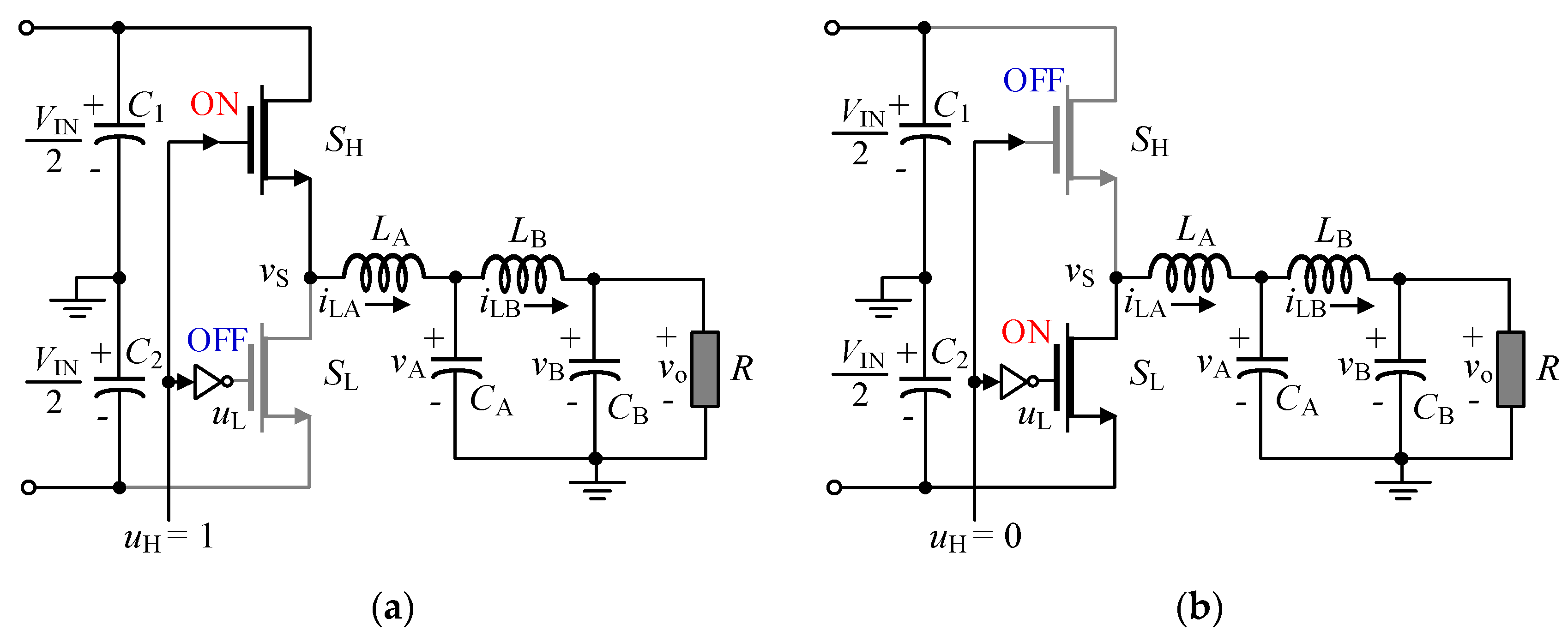
The role of the second LC stage is to improve the THD by reducing the residuals of switching harmonics [31]. It is important to investigate the effect of the additional LC stage on frequency response using average modeling, in order to ease the controller design process. Modeling of the power stage presented here neglects the non-idealities such as the forward voltage drop in the diode, conduction resistance of MOSFET and dead-time delay. Figure 1a,b shows the equivalent circuits during the two class-D operation modes determined by the control signals, i.e., uH and uL. These switching signals can attain the binary values; 1 and 0 for the on and off state of MOSFET respectively. For uH = 1, the low-side GaN cascode SL is in the off-state while the high-side SH is in the conduction state, and the voltage vs clamps to VIN/2 as shown in Figure 1a. Similarly, for uH = 0, voltage vs clamps to −VIN/2 as shown in Figure 1b. The dynamic equations of the converter for each switching state are expressed as
The subscript “A” and “B” depict parameters of the first and second LC stage. Thus, LA, iLA, and vA are the inductance of the first LC stage, the current through LA, and the voltage across CA respectively. VIN is the source, and vo is the output voltage. The average-model of the class-D amplifier, by combining (1) using duty cycle dH = avg(uH) is expressed as
where LB, iLB, and vB are the inductance of the second LC stage, the current through LB, and the voltage across CB, respectively, and the load resistance is denoted by R. The dynamics of the class-D amplifier may also be written in state-space form as
where x is the state vector, and f and g are functions of the state vector explicitly given in (4).
The open-loop transfer function from vS to output voltage vo can be deduced from (4) as:
Figure 2 shows the frequency response of the fourth-order class-D amplifier in an open-loop configuration. Using the filter values set (i) in Table 1 results in resonant frequencies at 14 kHz and 51 kHz, as shown in Figure 2a. The two frequencies are somewhat close to each other as the relations between the inductances and capacitances of the two stages are LA = 2LB and CB = 2CA respectively. The frequency response is repeated in Figure 2b using the filter values from the set (ii) in Table 1, resulting in resonant frequencies at 14 kHz and 114 kHz. It indicates that the first resonant frequency is independent of LB and merely depends on LA, CA, and CB. Moreover, the separation between the two frequencies determines the damping of the second resonance. The second frequency can be displaced adequately by using an appropriate integer multiplier n ≥ 2 such that LA = nLB [9]. It is also noted that the resonant peaking increases with the load resistance and approaches zero-damping under a no-load condition.
To improve the frequency response of fourth-order GaN class-D amplifier, the FFDISM controller is proposed. Two different sliding-surfaces are proposed; each includes an extra current term (either inductor or capacitor current of the first LC stage) in addition to voltage error in the state variables. The coefficients of the sliding-surfaces are determined using the stability condition. The controller using capacitor current is compared to the controller with an inductor current in terms of high-efficiency and ease of implementation. The simulation and experimental results are presented to verify the performance of the FFDISM controller using capacitor current feedback.
3. FFDISM Controller of Fourth-Order GaN Amplifier
The design starts by proposing a sliding-surface as a function of state-variables followed by the derivation of the equivalent control, and finally choosing the coefficients of the sliding-surfaces using stability condition [32,33]. Two different sliding-surfaces are proposed here; the first includes the inductor current feedback while the later employs capacitor current feedback.
3.1. Inductor Current Feedback
The state-variables for FFDISM controller are denoted by δ1 and δ2 and expressed as
where e is the voltage error between reference signal vref and scaled down output voltage βvo, iLA is inductor current feedback, ρ and β are scaling factors. Differentiating the set of equations in (6), substituting from (4) gives:
where m = 2dH − 1 is the modulation signal.
The sliding-surface is proposed as the weighted sum of δ1 and δ2 and expressed as
where the weights γ1 and γ2 are sliding coefficients. By differentiating the sliding-surface in (8), using (4), and finally solving Ṡ1 = 0 for mequ gives the equivalent control [34] as
where the equivalent control is bounded as |mequ| ≤ 1. By further manipulation, the equivalent control signal as a function of controller gains can be expressed as
where
The gains α1, α2, and α3 derived using the necessary existence and stability condition determines the controller performance. The selected range of gains using existence condition determines the region where state trajectory will always be directed to the sliding-surface. By satisfying the Lyapunov condition Ṡ1 × S1 < 0, gives the existence condition:
The stability condition can be derived by substituting Ṡ1 = 0, which results in the following characteristic equation
where the straightforward criterion γ2/γ1 > 0 ensures the asymptotic stability. Therefore, the ratio of sliding coefficients is chosen as γ2/γ1 = 1.5πfb where fb is the natural frequency of the closed-loop system. Using LA = 33 μH, fb = 10 kHz and β = ρ in (11) gives the controller gains as:
3.2. Capacitor Current Feedback
The controller design procedure is repeated using a different sliding-surface which involves capacitor current iCA. The state-variables for FFDISM controller are redefined as Δ1 and Δ2
where e is the voltage error between reference signal vref and scaled down output voltage βvo, β and σ are scaling factors. Differentiating Equation (15) and substituting (4) gives
The sliding-surface for the FFDISM controller is defined as
where ς1 and ς2 are sliding coefficients. The equivalent control [34] is obtained by differentiating the sliding-surface S2, using (4) and finally solving Ṡ2 = 0 for equivalent control mequ
By further manipulation, the equivalent control signal as a function of controller gains can be expressed as
where
The controller gains λ1, λ2, λ3, and λ4 are derived using existence and stability conditions. Satisfying the Lyapunov condition Ṡ2 × S2 < 0, ensures the existence condition:
The stability condition can be derived using Ṡ = 0, which gives the characteristic equation as
The criterion ς2/ς1 > 0 ensures stability. Therefore, the ratio of sliding coefficients is chosen as ς2/ς1 = πfb where fb is the natural frequency of the closed-loop system. The controller parameters, using fb = 10 kHz and β = σ in (20), are given as:
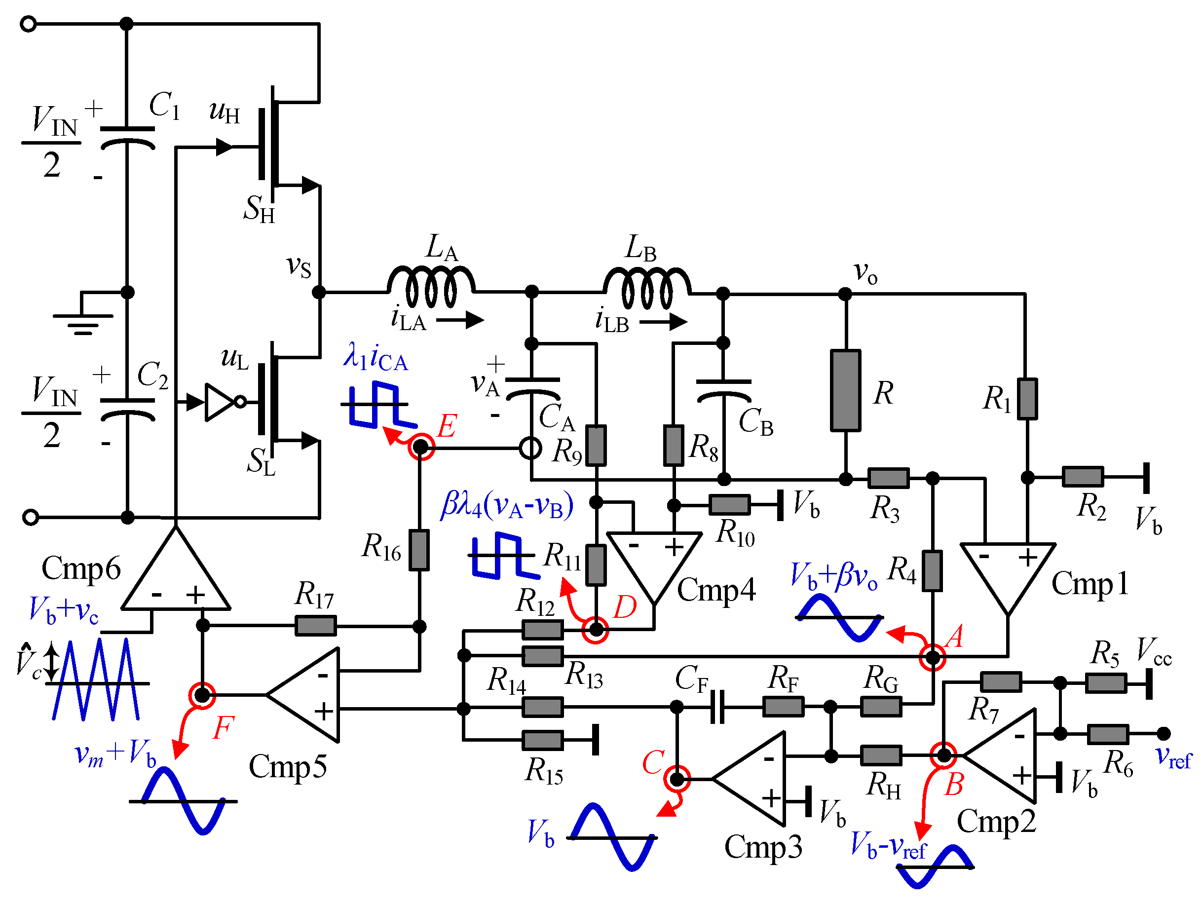
The two FFDISM configurations corresponding to sliding-surfaces S1 and S2 are implemented by translating their respective equivalent control equations to analog systems. The FFDISM controller implemented using (10) is shown in Figure 3a, where the difference between the scaled output voltage βvo and reference signal vref, is applied to the proportional integral (PI-type) controller. In addition to vo, it also requires feedback voltage vA and current iLA from the first LC stage. The closed-loop response is determined by the gains α2 − α3 and plays the important role of the error signal e processing. Similarly, Figure 3b shows the FFDISM controller involving the capacitor current iCA feedback implemented using (19) where the gains λ1 − λ4 determine the response of the closed-loop system. It is observed that the FFDISM controller for fourth-order class-D amplifier requires more feedback variables, i.e., beside iLA and iCA the controller in Figure 3a,b respectively requires βvA and β(vA − vB). These additional variables make the circuit implementation more challenging. Therefore, it is important to select the controller that in addition to shaping the frequency response also offers ease of circuit implementation.
4. Realization of FFDISM Controller
High switching frequency necessitates the analog implementation of the controller using low-cost, single-supply opamps. Figure 4 and Figure 5 show the circuit realization of FFDISM controllers for fourth-order GaN class-D amplifier, with additional iLA and iCA feedback respectively. For ease of reference, the controller involving inductor current and capacitor current is pointed as CNRL1 and CNRL2 respectively. Single-supply opamps are used due to its rail-to-rail input and low power consumption as compared to the dual-supply counterparts. The Vcc and Vb are opamps dc supply and mid-point bias voltage respectively. Here, both FFDISM designs are evaluated to find the one that offers ease of implementation, determined by the required number of opamps. The additional voltage feedback signals, i.e., vA in CNRL1 and β(vA − vB) in CNRL2 unanimously increases the opamp count. However, dc-biasing of iLA is required, which increases the opamp count in CNRL1 as compared to CNRL2.
Furthermore, the capacitor current iCA in CNRL2 is bidirectional and therefore, can be sensed using a low-cost current transformer as there is no saturation problem. A sense resistor RSC across the secondary of the current transformer converts the current signal into the voltage signal and adequately scales, i.e., λ1 = 0.01RSC. This RSC carries low-current and thus, does not affect the efficiency. On the other hand, the sense resistor for the inductor current iLA feedback in CNRL1 can cause a significant reduction in overall efficiency. It is concluded that CNRL2 offers improvement in efficiency and requires fewer numbers of opamps as compared to CNRL1. Therefore, FFDISM controller using the capacitor current iCA is finally implemented for experimental testing.
In Figure 5, the voltage at node A is the scaled and biased output voltage, with the scaling factor determined by the ratio β = R2/R1 = R4/R3 = 4 kΩ/100 kΩ. Meanwhile, Cmp2 inverts and adds bias Vb to vref as the waveform shows at node B, with the resistors R5 = R6 = R7 = 200 kΩ. The opamp Cmp3 serves as a proportional integral (PI-type) controller, where capacitor CF and resistors RF, RG, and RH together determine the proportional and integral gains as λ2 = RF RG and λ3 = 1/CFRG. Since modulating signal is referenced to Vb = +2.5 V, the carrier signal is also biased to the same dc-level, where its peak, denoted as hat{Vc} is given by βVIN/2 = 2 V.
A prototype of the fourth-order GaN class-D amplifier has been built using the GaN cascode transistor, with the top and bottom sides shown in Figure 6a,b respectively. GaN cascode is realized by combining a low-voltage Si MOSFET with a high-voltage GaN HEMT to exhibit low-conduction and switching power losses. The TPH3006PD (Transphorm Inc., San Jose, CA, USA) available in TO-220 package is used to realize the power circuit. A conventional totem-pole gate driver with a low-valued gate resistance of 3 Ω is used to enable fast switching. The parasitic inductances of the package are high, which is responsible for drain voltage overshoot followed during turn-off transient. Therefore, an resistor-capacitor (RC) snubber across the low-side GaN cascode is used to suppress undesired oscillations. Three 150 µF electrolytic capacitors are connected in parallel to achieve high bus capacitance and reduce the effect of interconnection inductances.
5. Results and Discussion
In this section, the performance of the proposed FFDISM controller is evaluated using simulation and experimental results. First, the frequency response and step response of the closed-loop system based on control diagram reduction are presented. This fundamental technique is useful to investigate the effect of the inner-loop on the compensation of resonance. Furthermore, computer–based circuit simulator i.e., Plexim Plecs is used to analyze the transient behavior of class-D amplifier using different resistive loads. Finally, experimental results are presented for validation of FFDISM controller.
5.1. Simulation Results
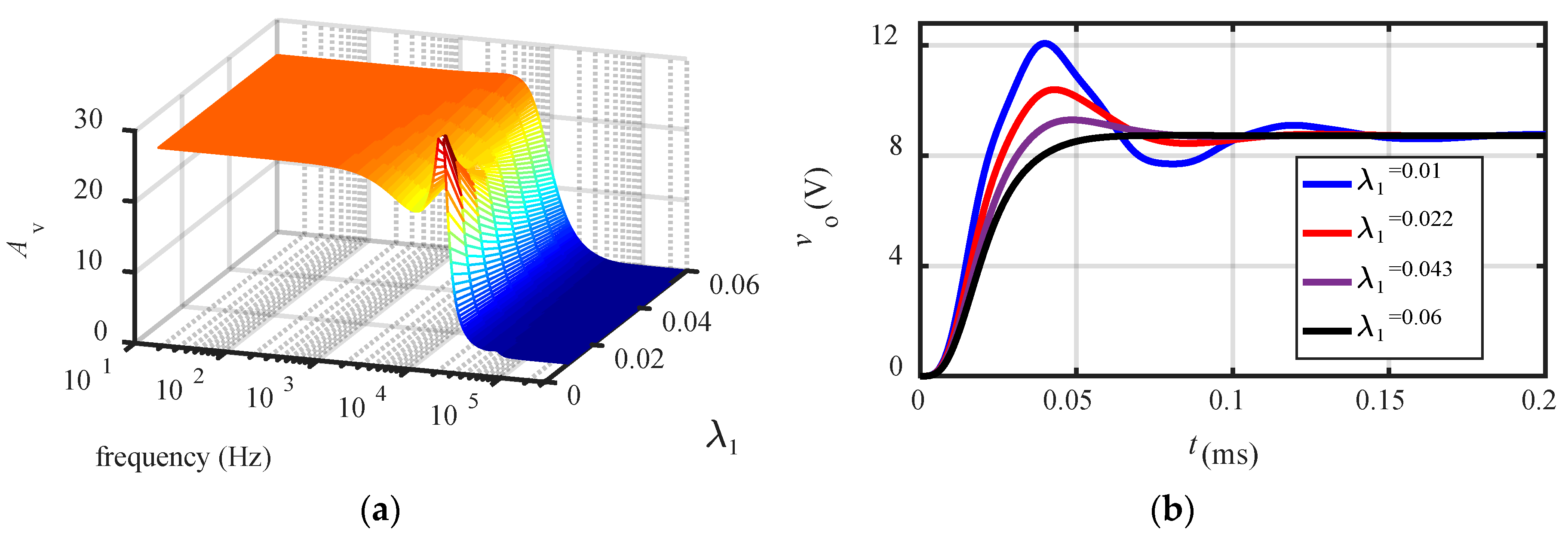
Figure 7a shows the multi-loop control diagram of the class-D amplifier, while the equivalent reduced form is shown in Figure 7b with the open-loop transfer functions Ho and Go given in (24) and (25) respectively:
where the parameters of the amplifier are given in Table 1 (value set i), selected using second-order Butterworth approximation. The feedback gains employed are λ4 = 0.08 and β = 0.04. Figure 8a shows the frequency response of the closed-loop class-D amplifier using frequency sweep ranging from 10 Hz to 300 kHz. The frequency response of the FFDISM-controlled amplifier is presented to investigate the significance of the inner-loop for different values of the capacitor current gain λ1. It is observed that the controller effectively mitigates the resonant peaks and promises a flatter frequency response, almost independent of the load. Further, the proposed control strategy is verified by analyzing the step response in Figure 8b. The voltage overshoot and oscillations decrease with an increase in the capacitor current gain λ1.
The transient response of fourth-order GaN class-D amplifier is analyzed using a circuit simulator, which offers a chance to evaluate the correctness of the proposed design. A close match to the experimental results can be obtained by adding the nonidealities to the simulation. Therefore, parasitic resistances of 500 mΩ and 200 mΩ are added to the filter inductors and capacitors, respectively. A sampling time of 1ns is used to capture the simulation results with adequate accuracy at a switching frequency of 100 kHz. Furthermore, a dead-time of 50 ns is introduced before every switching transition. Other factors such as delay in gate driver stage, jitters in PWM, finite rise and fall time of the gate signal are ignored; otherwise, the model takes a long time for solving.
The reference signal is a square wave of 1 kHz frequency, 50% duty cycle and 2 V peak-to-peak amplitude. Such a reference acts as a series of periodic step changes where the slew rate of the rising edge indicates the amplifier’s bandwidth. Simulations are performed using the resistive load of 7 Ω and 14 Ω to observe the change in the voltage overshoot and the settling time with the load. Figure 9a indicates that the response of the open-loop GaN class-D amplifier is strongly dependent on the load, and the observed voltage overshoot and settling time are 9.34 V and 0.15 ms, respectively, for R = 7 Ω. By increasing the load resistance to 14 Ω, voltage overshoot and settling time rises to 13.25 V and 0.21 ms respectively. The FFDISM controller using inductor current is also simulated, and results are shown in Figure 9b. The improvement in response is observed using the controller gains derived in (11). Finally, the simulation results for GaN class-D amplifier with FFDISM using the capacitor current obtained under different loads are presented in Figure 9c. The proposed FFDISM controller reduces the voltage overshoot and steady-state error to 0.41 V and 0.3 V, respectively, thereby proving its superiority.
5.2. Experimental Results
For experimental validation, a prototype of fourth-order class-D amplifier was implemented on PCB using GaN, available in TO-220 package. Single-supply opamps were used to translate the equivalent control equation in (19) into the analog controller.
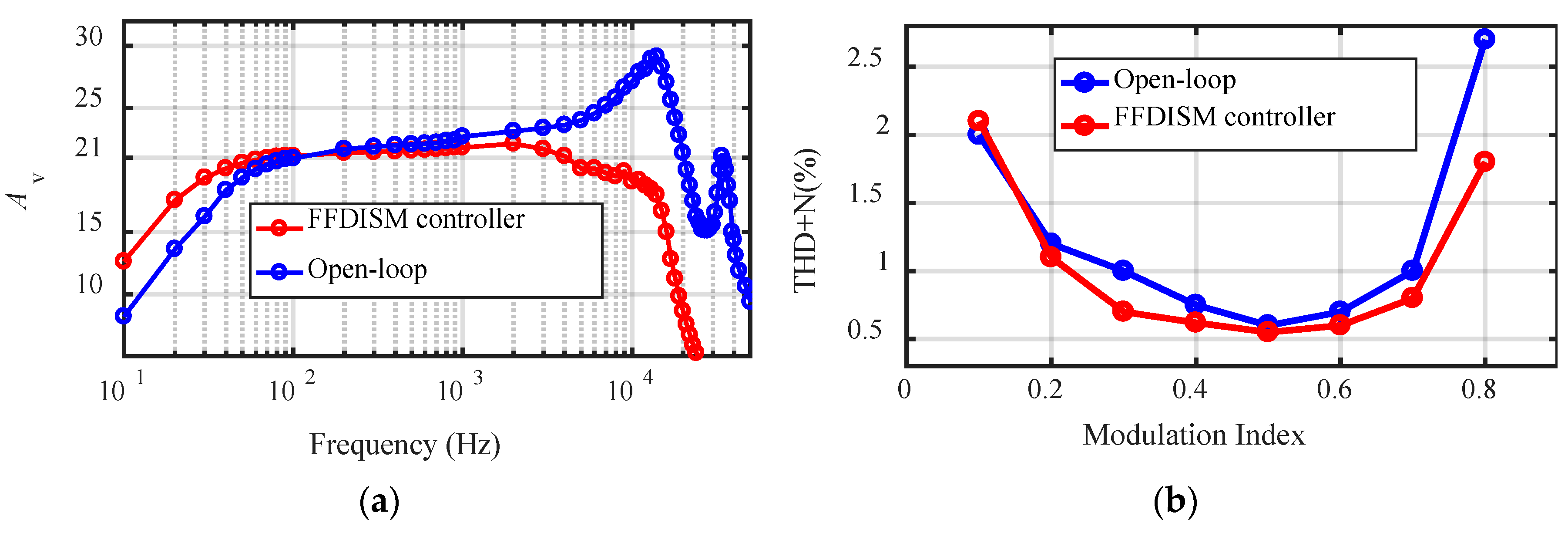
For measurement of the frequency response, sinusoidal reference signals (vref) of different frequencies ranging from 10 Hz to 50 kHz were applied using a signal generator, and the corresponding outputs were listed. The voltage gain (Av) was computed for open and closed-loop configurations, as the ratio of the reference vref to output voltage vo. Figure 10a shows the voltage gain plotted against the frequency of the reference signal when there is a 10 Ω resistive load. It is noted in open-loop (shown in blue), that the voltage gain at the 33 kHz resonant frequency is 29.3 which is successfully compensated by FFDISM controller as depicted in red.
Figure 10b shows the THD+N of GaN amplifier against the modulation index, defined as the ratio of the carrier to reference voltage and can range from 0 to 1. The output voltage vo was recorded using the data-acquisition card at 5 MSa/s sampling frequency, and the fast Fourier transform (FFT) was used to extract THD+N. It was observed that FFDISM controlled fourth-order class-D amplifier achieved improved THD+N as compared to open-loop architecture.
Figure 11a shows the experimental transient response of open-loop GaN class-D amplifier to a reference square wave of 1 kHz frequency. It is found that with a load resistance of 10 Ω, the resonant frequencies result in voltage overshoot of 5.2 V. Similarly, the transient response with FFDISM controller to 1 kHz reference square wave is shown in Figure 11b, with a recorded overshoot of 1.3 V. Thus it is validated, that the proposed controller improves the transient response of the fourth-order class-D amplifier.
Furthermore, the scalogram analysis was performed, which illustrated a combined time and frequency-domain response of the amplifier. The wavelet transform was applied to represent the output voltage vo as a weighted sum of the limited duration wavelet functions. Figure 12a shows the scalogram of the transient response in Figure 11a. A horizontal line in the figure represents a particular harmonic in the output waveform with its frequency on the y-axis and magnitude given on the color-bar. Since the square wave is a weighted sum of odd harmonics, the parallel lines below 16 kHz can synthesize it with adequate accuracy. Similarly, the line at 100 kHz is due to residual switching noise. There is a noticeable activity in the time interval 2–4 ms and 7–9 ms due to voltage ringing, corresponding to the resonant frequencies at 12.7 kHz and 33 kHz. Figure 12b shows the scalogram of the transient response in Figure 11b. The shrunken oval-shaped region and the reduction in magnitude noted on the color-bar verify the effectiveness of the FFDISM controller.
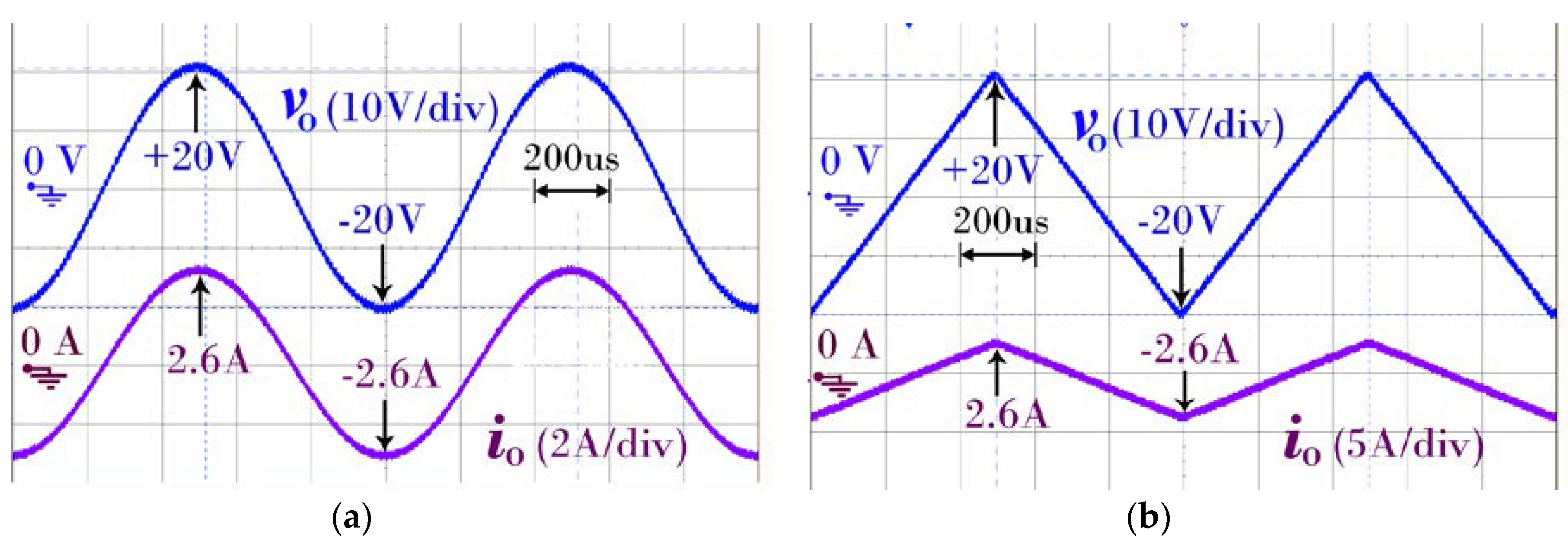
Finally, sinusoidal and triangular signals were generated using the FFDISM controlled GaN class-D amplifier. Figure 13a shows the 1 kHz sinusoidal output voltage vo and the corresponding current io of the fourth-order amplifier. Similarly, for a 1 kHz triangular reference, output voltage vo and current io are shown in Figure 13b. Thus, the effectiveness of the FFDISM controller, proposed for fourth-order class-D amplifier has been validated. Figure 14 illustrates the efficiency of GaN class-D amplifier at different operating powers. It is observed that at 150 W power, the amplifier achieves 93% efficiency. Moreover, the efficiency and bandwidth of the proposed class-D amplifier are compared in Table 2, against the hysteretic modulation-based implementation. It indicates that the class-D amplifier with PWM not only gets rid of the variable switching frequency but also improves the efficiency by reducing switching losses.
6. Conclusions
The FFDISM controller has been successfully applied to the GaN-based fourth-order class-D amplifier. The fourth-order filter has been used to improve the THD of class-D amplifiers, operating at a relatively lower switching frequency. Two different FFDISM structures were proposed using the inductor and capacitor current. The advantages offered by the FFDISM controller using the capacitor current over the counterpart using inductor current feedback are listed as: The bidirectional nature of the capacitor current demands a low-cost current-transformer for feedback; the current sense circuit does not affect the overall efficiency; and reduced opamp are required for circuit realization. A prototype of the amplifier was implemented on a PCB. The experimental results revealed that the proposed FFDISM controller effectively flattens the frequency response of the fourth-order amplifier, and results in THD and voltage overshoot of 0.6% and 1 V respectively.
Author Contributions
H.Z. and X.Z. contributed equally to the research presented here. H.Z. and X.Z. conceived and designed the experiments. H.Z. performed the experiments, analyzed the data and wrote the paper. X.W. and H.A. provided significant comments and technical feedback throughout the research. S.K. reviewed and improved the paper.
Conflicts of Interest
The authors declare no conflict of interest.
References
- Bagger, R.; Sjoland, H. Broadband LDMOS 40 W and 55 W integrated power amplifiers. In Proceedings of the 2017 IEEE MTT-S International Microwave Symposium, Honololu, HI, USA, 4–9 June 2017; pp. 1950–1952. [Google Scholar]
- Bosi, G.; Raffo, A.; Trevisan, F.; Vadalà, V.; Crupi, G.; Vannini, G. Nonlinear-embedding design methodology oriented to LDMOS power amplifiers. IEEE Trans. Power Electron. 2018, 33, 8764–8774. [Google Scholar] [CrossRef]
- Ramella, C.; Piacibello, A.; Quaglia, R.; Camarchia, V.; Pirola, M. High Efficiency Power Amplifiers for Modern Mobile Communications: The Load-Modulation Approach. Electronics 2017, 6, 96. [Google Scholar] [CrossRef]
- Thorsell, M.; Fagerlind, M.; Andersson, K.; Billström, N.; Rorsman, N. An X-band AlGaN/GaN MMIC receiver front-end. IEEE Microw. Wirel. Compon. Lett. 2010, 20, 55–57. [Google Scholar] [CrossRef]
- Nalli, A.; Raffo, A.; Crupi, G.; D’Angelo, S.; Resca, D.; Scappaviva, F.; Salvo, G.; Caddemi, A.; Vannini, G. Gan hemt noise model based on electromagnetic simulations. IEEE Trans. Microw. Theory Tech. 2015, 63, 2498–2508. [Google Scholar] [CrossRef]
- Recht, F.; Huang, Z.; Wu, Y. Characteristics of Transphorm GaN Power Switches. Application Note AN-0002. Available online: https://www.transphormchina.com/en/ (accessed on 19 October 2018).
- Saito, W.; Takada, Y.; Kuraguchi, M.; Tsuda, K.; Omura, I. Recessed-gate structure approach toward normally off high-voltage AlGaN/GaN HEMT for power electronics applications. IEEE Trans. Electron Devices 2006, 53, 356–362. [Google Scholar] [CrossRef]
- Su, L.Y.; Lee, F.; Huang, J.J. Enhancement-mode GaN-based high-electron mobility transistors on the Si substrate with a p-type GaN cap layer. IEEE Trans. Electron Devices 2014, 61, 460–465. [Google Scholar] [CrossRef]
- Quan, S.; Hao, Y.; Ma, X.; Xie, Y.; Ma, J. Enhancement-mode AlGaN/GaN HEMTs fabricated by fluorine plasma treatment. J. Semicond. 2009, 30, 124002. [Google Scholar]
- Jung, D.Y.; Park, Y.; Lee, H.S.; Jun, C.H.; Jang, H.G.; Park, J.; Kim, M.; Ko, S.C.; Nam, E.S. Design and evaluation of cascode GaN FET for switching power conversion systems. ETRI J. 2017, 39, 62–68. [Google Scholar] [CrossRef]
- Persson, E. How 600 V GaN Transistors Improve Power Supply Efficiency and Density. Power Electron. Eur. 2015, 2, 22–24. [Google Scholar]
- Jiang, X. Fundamentals of Audio Class D Amplifier Design: A Review of Schemes and Architectures. IEEE Solid-State Circuits Mag. 2017, 9, 14–25. [Google Scholar] [CrossRef]
- Cai, W.; Huang, L.; Wang, S. Class D Power Amplifier for Medical Application. Inform. Eng. Int. J. 2016, 4, 9–15. [Google Scholar] [CrossRef]
- Strasser, T. Real-Time Simulation Technologies for Power Systems Design, Testing, and Analysis. IEEE Power Energy Technol. Syst. J. 2015, 2, 63–73. [Google Scholar]
- Boillat, D.O.; Friedli, T.; Mühlethaler, J.; Kolar, J.W.; Hribernik, W. Analysis of the design space of single-stage and two-stage LC output filters of switched-mode AC power sources. In Proceedings of the 2012 IEEE Power and Energy Conference at Illinois, Champaign, IL, USA, 24–25 February 2012; pp. 1–8. [Google Scholar]
- Bloechl, M.; Bataineh, M.; Harrell, D. Class D Switching Power Amplifiers: Theory, Design, and Performance. In Proceedings of the IEEE SoutheastCon, Greensboro, NC, USA, 26–29 March 2004; pp. 123–146. [Google Scholar]
- Yu, Y.; Tan, M.T.; Goh, W.L.; Cox, S.M. A dual-feedforward carrier-modulated second-order class-D amplifier with improved THD. IEEE Trans. Circuits Syst. II Express Briefs 2012, 59, 35–39. [Google Scholar] [CrossRef]
- Chun, K.L.; Meng, T.T. A class D amplifier output stage with low THD and high PSRR. In Proceedings of the 2009 IEEE International Symposium on Circuits and Systems, Taipei, Taiwan, 24–27 May 2009; pp. 1945–1948. [Google Scholar]
- Künzi, R. Passive Power Filters. In Proceedings of the CAS-CERN Accelerator School: Power Converters, Baden, Switzerland, 7–14 May 2014; pp. 265–289. [Google Scholar]
- Cortes, P.; Boillat, D.O.; Ertl, H.; Kolar, J.W. Comparative evaluation of multi-loop control schemes for a high-bandwidth AC power source with a two-stage LC output filter. In Proceedings of the 2012 International Conference on Renewable Energy Research and Applications, Nagasaki, Japan, 11–14 November 2012; pp. 1–10. [Google Scholar]
- Boillat, D.; Krismer, F.; Kolar, J. Design Space Analysis and ρ-η Pareto Optimization of LC Output Filters for Switch-Mode AC Power Sources. Power Electron. IEEE Trans. 2015, 30, 6906–6923. [Google Scholar] [CrossRef]
- Nielsen, D.; Knott, A.; Andersen, M.A.E. Class D audio amplifier with 4th order output filter and self-oscillating full-state hysteresis based feedback driving capacitive transducers. In Proceedings of the 2014 16th European Conference on Power Electronics and Applications, Lappeenranta, Finland, 26–28 August 2014; pp. 1–7. [Google Scholar]
- Ablay, G. Robust integral controllers for high-order class-D power amplifiers. Power Electron. IET 2017, 11, 1–7. [Google Scholar] [CrossRef]
- Ge, T.; Chang, J.S.; Shu, W.; Tan, M.T. Modeling and Analysis of PSRR in Analog PWM Class D Amplifiers. In Proceedings of the 2006 IEEE International Symposium on Circuits and Systems, Island of Kos, Greece, 21–24 May 2006; pp. 1386–1389. [Google Scholar]
- Shu, W.; Chang, J.S. THD of closed-loop analog PWM Class-D amplifiers. IEEE Trans. Circuits Syst. I Regul. Pap. 2008, 55, 1769–1777. [Google Scholar] [CrossRef]
- Tan, S.C.; Lai, Y.M.; Tse, C.K. Sliding Mode Control of Switching Power Converters-Techniques and Implementation; CRC Press: Boca Raton, FL, USA, 2012. [Google Scholar]
- Tan, S.-C.; Lai, Y.M.; Tse, C.K.; Cheung, M.K.H. A fixed-frequency pulsewidth modulation based quasi-sliding-mode controller for buck converters. IEEE Trans. Power Electron. 2005, 20, 1379–1392. [Google Scholar] [CrossRef]
- Pradhan, R.; Subudhi, B. Double integral sliding mode MPPT control of a photovoltaic system. IEEE Trans. Control Syst. Technol. 2016, 24, 285–292. [Google Scholar] [CrossRef]
- Jiao, Y.; Luo, F.L.; Zhu, M. Generalised modelling and sliding mode control for n-cell cascade super-lift DC–DC converters. IET Power Electron. 2011, 4, 532–540. [Google Scholar] [CrossRef]
- Chincholkar, S.H.; Chan, C.Y. Design of fixed-frequency pulsewidth-modulation-based sliding-mode controllers for the quadratic boost converter. IEEE Trans. Circuits Syst. II Express Briefs 2017, 64, 51–55. [Google Scholar] [CrossRef]
- Maislinger, F.; Ertl, H.; Stojcic, G.; Holzner, F. Control Loop Design for Closed-Loop Class-D Amplifiers with 4th Order Output Filter. In Proceedings of the PCIM Europe 2017; International Exhibition and Conference for Power Electronics, Intelligent Motion, Renewable Energy and Energy Management, Nuremberg, Germany, 16–18 May 2017; pp. 1193–1200. [Google Scholar]
- Bacha, S.; Munteanu, I.; Bratcu, A. Power Electronic Converters Modeling and Control. Adv. Textb. Control Singal Process. 2014, 454, 454. [Google Scholar]
- Labbe, B.; Allard, B.; Shi, X.-L. Design and stability analysis of a frequency controlled sliding-mode buck converter. IEEE Trans. Circuits Syst. I Regul. Pap. 2014, 61, 2761–2770. [Google Scholar] [CrossRef]
- Rojas-Gonzalez, M.A.; Sanchez-Sinencio, E. Design of a Class D Audio Amplifier IC Using Sliding Mode Control and Negative Feedback. IEEE Trans. Consum. Electron. 2007, 53, 609–617. [Google Scholar] [CrossRef]
- Lu, J.; Gharpurey, R. Design and analysis of a self-oscillating class D audio amplifier employing a hysteretic comparator. IEEE J. Solid-State Circuits 2011, 46, 2336–2349. [Google Scholar] [CrossRef]
Figure 1.
Equivalent circuits of fourth-order GaN class-D amplifier when (a) uH = 1 (b) uH = 0.

Figure 2.
Open-loop frequency response of GaN class-D amplifier with fourth-order filter using (a) value set-i in Table 1 and (b) value set-ii in Table 1.

Figure 3.
FFDISM controller of fourth-order class-D amplifier using (a) iLA feedback (CNRL1) (b) iCA feedback (CNRL2).
Figure 3.
FFDISM controller of fourth-order class-D amplifier using (a) iLA feedback (CNRL1) (b) iCA feedback (CNRL2).

Figure 4.
Circuit realization of FFDISM controller with iLA feedback (CNRL1).

Figure 5.
Circuit realization of FFDISM controller with iCA feedback (CNRL2).

Figure 6.
Prototype of GaN class-D amplifier (a) top-side (b) bottom side.

Figure 7.
Closed-loop schematic of the class-D amplifier: (a) multi-loop form (b) reduced form.

Figure 8.
Effect of capacitor current iC feedback on damping of fourth-order class-D amplifier (a) closed-loop frequency response for different λ1 and (b) step response for different λ1.
Figure 8.
Effect of capacitor current iC feedback on damping of fourth-order class-D amplifier (a) closed-loop frequency response for different λ1 and (b) step response for different λ1.

Figure 9.
Simulation-based transient response of (a) open-loop GaN class-D amplifier; (b) FFDISM controller using inductor current; (c) FFDISM controller using capacitor current.
Figure 9.
Simulation-based transient response of (a) open-loop GaN class-D amplifier; (b) FFDISM controller using inductor current; (c) FFDISM controller using capacitor current.

Figure 10.
(a) Frequency response of the open-loop GaN class-D amplifier and with FFDISMC (b) THD+N the of open-loop GaN class-D amplifier and with FFDISMC.
Figure 10.
(a) Frequency response of the open-loop GaN class-D amplifier and with FFDISMC (b) THD+N the of open-loop GaN class-D amplifier and with FFDISMC.

Figure 11.
Experimental results transient response of: (a) open-loop GaN class-D amplifier; (b) GaN class-D amplifier with FFDISMC.
Figure 11.
Experimental results transient response of: (a) open-loop GaN class-D amplifier; (b) GaN class-D amplifier with FFDISMC.

Figure 12.
Experimental magnitude scalogram of GaN class-D amplifier: (a) open-loop; (b) with FFDISM controller.
Figure 12.
Experimental magnitude scalogram of GaN class-D amplifier: (a) open-loop; (b) with FFDISM controller.

Figure 13.
(a) Experimental result of GaN class-D amplifier with FFDISM controller output voltage vo and load current io and (b) output voltage vo for reference sine wave vref.
Figure 13.
(a) Experimental result of GaN class-D amplifier with FFDISM controller output voltage vo and load current io and (b) output voltage vo for reference sine wave vref.

Figure 14.
The efficiency of GaN class-D amplifier at different power.


Table 1.
Parameters of GaN class-D amplifier with fourth-order filter.
| Parameter | Symbol | Value Set | |
|---|---|---|---|
| i | ii | ||
| source voltage | VIN | 100 V | 100 V |
| first stage filter | LA, CA | 36 µH, 1 µF | 36 µH, 1µF |
| second stage filter | LB, CB | 18 µH, 2 µF | 3 µH, 2 µF |
© 2018 by the authors. Licensee MDPI, Basel, Switzerland. This article is an open access article distributed under the terms and conditions of the Creative Commons Attribution (CC BY) license (http://creativecommons.org/licenses/by/4.0/).
Share and Cite
MDPI and ACS Style
Zaman, H.; Zheng, X.; Wu, X.; Khan, S.; Ali, H. A Fixed-Frequency Sliding-Mode Controller for Fourth-Order Class-D Amplifier. Electronics 2018, 7, 261. https://doi.org/10.3390/electronics7100261
AMA Style
Zaman H, Zheng X, Wu X, Khan S, Ali H. A Fixed-Frequency Sliding-Mode Controller for Fourth-Order Class-D Amplifier. Electronics. 2018; 7(10):261. https://doi.org/10.3390/electronics7100261
Chicago/Turabian StyleZaman, Haider, Xiancheng Zheng, Xiaohua Wu, Shahbaz Khan, and Husan Ali. 2018. "A Fixed-Frequency Sliding-Mode Controller for Fourth-Order Class-D Amplifier" Electronics 7, no. 10: 261. https://doi.org/10.3390/electronics7100261
Note that from the first issue of 2016, this journal uses article numbers instead of page numbers. See further details here.