SystemC/TLM Controller for Efficient NAND Flash Management in Electronic Musical Instruments


1
Department of Information Engineering, Marche Polytechnic University, I-60131 Ancona, Italy
2
KORG Italy S.p.A., I-60027 Osimo, Italy
*
Author to whom correspondence should be addressed.
Electronics 2018, 7(5), 75; https://doi.org/10.3390/electronics7050075
Submission received: 20 April 2018
/
Revised: 12 May 2018
/
Accepted: 16 May 2018
/
Published: 18 May 2018
(This article belongs to the Special Issue All-Digital Time-Mode Approaches for Mixed Analog-Digital Signal Processing)
Abstract
:The design of an efficient memory subsystem is a fundamentally challenging task in the design of electronic equipment. The storage hierarchy chosen for a particular design has a significant impact on the overall performance and cost. Flash memory often contains the boot code, operating system kernel, device drivers, middleware, and other application-specific software that can result in megabytes of non-volatile stored data. To maximize the performance, data are moved from non-volatile memory to faster SDRAM (synchronous dynamic random-access memory). Non-volatile memory technologies reach a performance level close to that of dynamic RAMs with the additional benefit of persistent data storage. When cost is critical, an approach where the data are managed directly from non-volatile memory can be used. In this case the non-volatile memory subsystem is constantly accessed to retrieve data. The deep understanding of the system architecture is critical to identify any factor that affects memory performance and the resulting system performance; particularly in specific applications with stricter requests like streaming audio when more than one hundred data streams must be handled in a real-time environment and sound must be generated with a total latency of a few milliseconds. This article reports the development of the system-level model of a controller in a SystemC simulation environment capable of optimizing the use of NAND type flash memories for storage and playback of audio samples in real-time music applications, with the aim of reducing the quantity of the system SDRAM memory, thus lowering the cost of the final product, while still providing the most high-fidelity sound experience.
1. Introduction
Digital electronic musical instruments generate sound essentially in four ways: physical modeling synthesis, subtractive synthesis, Frequency Modulation (FM) synthesis, and Pulse Code Modulation (PCM) synthesis. Physical modeling synthesis is a technique that computes the sound generation by using mathematical algorithms to simulate the physical sound source. In subtractive synthesis, a sound source that is rich in harmonics is filtered and properly subtracts the harmonics to create the desired sound. Then, envelopes are used to shape the attack, decay, sustain, and release of the sound. In FM synthesis, a carrier waveform (sine, square, triangle…) is modulated by another wave to obtain a complex waveform.
PCM synthesis is widely adopted and some aspects related to its implementation will be considered in this work. PCM uses samples as a primary sound source. The samples are the recording of a particular sound generated by a given physical acoustic instrument. In this work we will investigate the way to face some of the problems related to the PCM technique. The recorded audio samples can be considerably large, occupying a great amount of memory.
Digital processing algorithms and a digital signal processor (DSP) are used to modify the recorded sound, in order to recreate the full music extent and a realistic sound perception.
One of the most important effects applied on the recorded samples is pitch shifting, which is the modification of the intonation of a note by shifting the spectrum of the original signal.
Polyphony is the ability of an electronic instrument to process and simultaneously play a certain number of voices. The fidelity with respect to the physical acoustic sound is improved by increasing the number of voices played simultaneously.
The arrangement is another typical feature of an electronic musical instrument. The arrangement allows the setting-up of a virtual band playing with the musician and following the melody that is being produced, creating a feeling similar to that of a concert.
The software executed on the instrument generates different tracks to simulate a virtual musician by creating all the voices related to it, as summarized in Figure 1.
These mechanisms of sound generation must be performed in a very short time to reduce as much as possible the latency that exists between a certain action, such as the activation of a key, and the actual perception of the produced sound. The latency is mainly due to the time needed for the transfer of data from the memory where they are stored to the DSP that processes them. Another key requirement for an electronic instrument is that the music generation must always be continuous, in any condition of use and under any loading level of the operating system.
The memory device used for the storage of the recordings and the related data access algorithm must ensure two basic features: the minimum value required for data read throughput and a sufficiently low and constant maximum latency level. A straightforward solution is the use of a large RAM memory where all audio samples are copied from a non-volatile memory; this configuration implies a high cost and a long system start-up time. One possible smarter and cheaper solution involves the use of a non-volatile memory fast enough to withstand all audio sample requests only when they are actually needed while guaranteeing a sufficiently low data latency.
This paper presents the study of the possibility to use the NAND-type flash memories for the management of audio samples in real-time musical applications and the development of a high-performance controller with the purpose of optimizing the entire memory requirement and thus lowering the cost of the final product.
2. NAND Flash Memory
In a modern electronic musical instrument that uses PCM synthesis for sound generation, the audio samples are usually saved in a non-volatile mass storage device represented by a hard-disk or one or more Solid State Drives (SSD) using NOR or NAND flash technology. Generally, these memories do not have the speed and latency characteristics that are required for high-performance real-time sound generation, for this reason during the startup of the instrument all audio samples must be copied to the main system memory, typically consisting of very fast DDR SDRAMs. This mechanism implies high startup times and considerable cost due to the large amount of required SDRAM memory. Technological advances regarding in particular the NAND flash memory are leading to fast access times and high transfer rates [1,2]. Therefore, it is possible to manage the data directly from the non-volatile storage, thus avoiding the complete copy in a faster and expensive memory whose size can be consequently strongly reduced.
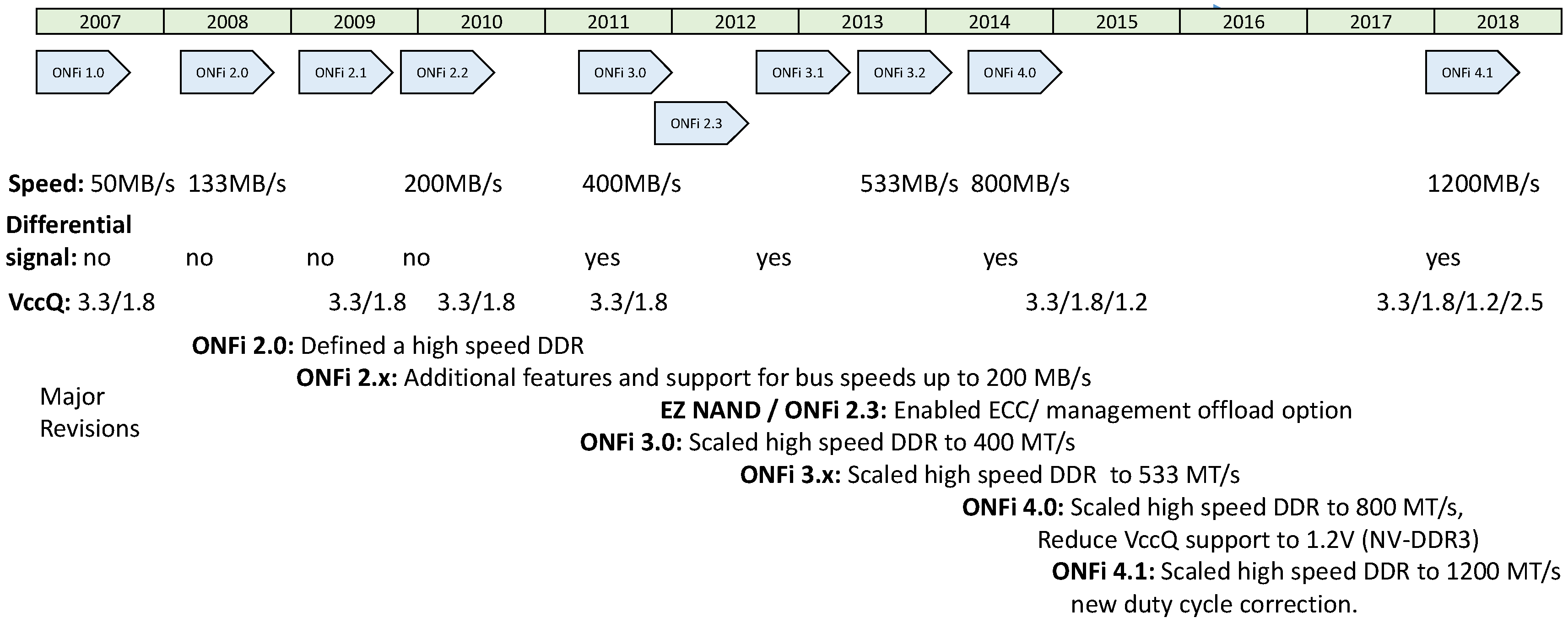
The Open NAND Flash Interface (ONFi) organization [3] comprises suppliers and developers of NAND Flash memory components whose goal is to define a uniform NAND Flash component interface. The first version of the ONFi standard ONFi 1.0 was realised on December 2006. From 2006 to 2018 many other versions were realized, as shown in Figure 2, due to fast technological innovation.
The ONFi standard defines the architecture level, signal level details, and low levels details such as: pin assignment, maximum time delay, power supply, single, or differential signaling. ONFi supports four different data interface types: SDR, NV-DDR, NV-DDR2, and NV-DDR3 [3]. The SDR data interface is the traditional NAND interface that uses the signal RE_n to latch data read, WE_n to latch data written, and does not include a clock. The NV-DDR data interface is double data rate (DDR), includes a clock that indicates when commands and addresses should be latched, and a data strobe that indicates when data should be latched. The NV-DDR2 data interface is double data rate and includes additional capabilities for scaling speed like on-die termination and differential signaling. The NV-DDR3 data interface includes all NV-DDR2 features, but operates at VccQ = 1.2 V.
NOR memories are able to read and write single bytes, NAND memories must access on groups of bytes called pages and they erase groups of pages called blocks. Therefore, NOR memories perform much faster access to single data if compared with NAND memories. NOR flash memory is well suited for code storage and execute-in-place applications, while NAND flash memory is suitable for data storage, since they perform faster sequential read, write, or erase [3,4]. This makes NAND memories well suited for the application of sound generation with a typical traffic of a continuous streaming of 16 KB blocks of data, as will be shown in Section 3.
The typical organization of NAND memories can be represented by a hierarchical structure comprised of the following different elements [3,4,5]:
- page: it contains a number of data bytes and a “spare” area dedicated, for example, to the storage of error correction codes (ECC);
- block: basic erasable unit containing a number (multiple of 32) of pages;
- logic unit (LUN): the minimum unit able to execute commands independently and to report the execution status. Each memory consists of one or more LUNs, each one containing a number of blocks and one or more page-registers: the page register is a volatile memory with the same size of a page and it is used as a buffer for read and write operations
NAND memories are organized in blocks, each block consists of a fixed number of pages. The erase operation is performed per block, whereas reads and writes are performed per page. Before data can be written to a page the page must be erased, and each erase operation must have a coarser granularity when compared to the write operation. The effect is that data are moved (or rewritten) more times. This effect is called write amplification. Write amplification consumes bandwidth and reduces the time the memory can reliably operate.
It is also important to consider the specific limits of the NAND flash technology that can lead to the loss or to the corruption of the stored data: charge drift, read disturb, and program disturb. Therefore, the controller usually manages not only the operations of reading and writing, but appropriate strategies to prevent loss of data.
The software managing the flash memories is called Flash Translation Layer (FTL). Its main functionalities are [4,5,6,7,8]:
- address translation: The main task of the FTL is the address translation. The address translation layer translates logical addresses from the file system into physical addresses on flash devices. Flash memory uses relocate-on-write, also called out-of-place write, or write-in-place. If write-in-place is used, flash has high latency due to the necessary reading, erasing, and writing of the entire block. Relocate-on-write requires a garbage-collection process, which results in additional read and write operations.
- wear leveling: Each block can be put through a limited number of erase cycles before becoming unreliable. The number of program/erase cycles is limited to about 10,000–1,000,000 times [3,4]. Wear leveling is the algorithm that manages erase and write operations trying to ensure that every block is written an equal number of times to all other blocks.
- garbage collection: It is used to pick the next best block to erase and rewrite. If the data in some of the pages of the block are no longer needed, only the pages with good data must be maintained. The garbage collector seeks to merge partially-used blocks collecting only the good pages of the blocks that are rewritten all together into another previously erased empty block. The partially used blocks are then erased and free. Garbage collection is a substantial component of write amplification on the SSD.
- bad block management: NAND Flash memories suffer from the presence of locations whose reliability is not guaranteed, called bad blocks. The bad block management maintains a map of bad blocks, created during factory initialization and updated during the device life cycle.
- error correction: The error during read and write in a NAND is a problem to be faced especially for high speed memories. Some memories embed an error correction code (ECC) inside the memory block. The ECC corrects one or more errors in the data. The most popular are Reed–Solomon codes and Bose–Chaudhuri–Hocquenghem codes (called BCH codes). While the encoding takes few controller cycles of latency, the decoding phase can take a large number of cycles and visibly reduce read performance as well as the memory response time at random access. A simple model of the ECC consists only in taking into account the time required for the ECC itself. When data correction is not possible, high level strategies must be carried out. Those strategies may consist in read retry or write retry.
- cache operations: NAND memories with two page-registers can use one of them as a cache. Part of the time of an operation is given by the data transfer between the controller and chip, so it is possible to take advantage of the page registers by copying the data related to the next operation in the cache during the busy time of the LUN, lowering the overall operations wait time and increasing the overall throughput.
- multi-LUN operations: in memory models with multiple LUNs some operations can be executed in parallel on each logical drive, thus greatly increasing performance. Each memory bank shares the communication interface and part of the control logic; therefore, the speed of the memory is not really multiplied with parallel operations. Operations performed by the LUN within the same chip have constraints on type and on page addresses limiting the operational capabilities of the controller.
- interleaving: this technique is similar to multi-LUN, but in this case separate memories are used sharing the same I/O physical interface.
- multi-channel: this method consists in the use of multiple memory chips [6] controlled in a totally independent manner on dedicated I/O interfaces. The average throughput grows proportionally to the number of channels, but there is also an increase in the logic complexity of the controller and in the connections to the memory devices.
Recently, many methods and tools for the exploration of the NAND flash memory architecture have been proposed and several SSD simulators have been developed [4,5,6,7,8,9,10,11,12,13].
Kang et al. in [4] present the design and implementation of a high-performance NAND flash-based storage system that exploits I/O parallelism from multiple channels and multiple NAND flash memory chips.
A simulator, written as a single-threaded program C++, used to evaluate flash memories performances is reported in [9].
Lee et al. [10] developed a clock accurate simulator for hardware components description. It allows the optimization of FTL able to manage the concurrency of multiple chips and buses.
Jung et al. in [11] implemented a simulator in C++ that models the characteristics of the hardware components with clock accurate description.
Hu et al. in [12] present a probabilistic analysis of write amplification in flash-based SSDs. They developed their own event-driven simulator written in Java on which the flash memory simulator is based. Flash chips are modeled according to ONFi 1.0.
The tool proposed in [13], called SSDexplorer, is a complete tool written in SystemC for the design exploration of SSD architecture. Furthermore, the paper presents an interesting overview of SSD emulators with the aim of evidencing the characteristics of the tool they proposed, and the different abstraction levels that can be used to describe the SSD architecture.
The authors in [13] state that a high abstraction level allows faster performance estimations, but the accuracy is lost. SSDexplorer uses different abstraction levels for the different components, selecting the most suitable modeling style for each SSD component to accurately quantify the performance. Some blocks have been described by pin-accurate cycle accurate models, some by transaction-level cycle-accurate, and some by parametric time delay models. For example, the controller that performs read/write operations on the NAND flash memory arrays has been described as a pin-accurate cycle accurate using the ONFi 2.0 standard. This choice has the consequence that many changes on the block must be made to simulate a newer version on the ONFi standard.
3. Performance Requirements for High-Quality Sound Generation
During a real-time audio streaming, the audio tracks are generated from the samples stored in the nonvolatile NAND flash memory. The SDRAM is used only as a buffer.
When the system boots up, the first part of each sampled sound is copied in the central memory. Then, new portions of audio samples (called a streaming block) are copied in the central memory, when the musician starts playing. This technique greatly reduces the size of the volatile memory, thus reducing costs and latency. The NAND memory must be fast enough to provide the next streaming block before the playback of the current one is completed.
The playing time of a streaming block depends on different parameters. Typical values of a single streaming block are: streaming block size: 16 KB; sample precision: 16 bit sampling frequency: 48 kHz; pitch factor: from 0.5 to 2. These values determine a variable playing time, from about 85 ms to 333 ms, according to the considered pitch factor; consequently, the bit rate of the stream associated to a single block varies from about 46.9 KB/s to 187.5 KB/s.
The polyphony of a modern electronic musical instrument is at least 128. That is the instrument plays 128 voices at the same time. Next generation instruments will play 256 voices at the same time. Therefore, in this work we consider a 256 polyphony. Previous specifications are valid for the streaming of a single voice, but to determine the heaviest workload condition it is important to consider the case of the streaming engine playing all manageable voices at the same time and all modulated with the maximum pitch. Given these hypotheses, the audio generation engine requests 256 streaming blocks to the memory, each with a size of 16 KB, these data must be read and transferred to the SDRAM in less than 85 ms. The overall size of all buffers is 4 MB, which implies a throughput of about 48 MB/s. Furthermore, it must be considered that the memory is not subjected to 4 MB requests but to a flow of 16 KB requests randomly distributed over time.
The ability of the Flash to serve read or write transactions is measured by the number of “Input/Output Operations Per Second” (IOPS), typically with a traffic of random requests of a small amount of data (4 KB). The 256 polyphony musical synthesis requires 4 × 256 requests of 4 KB each every 85 ms, that is 4 × 256/0.085 = 12,047 number of IOPS. This value is much higher than what is currently offered by the market of high performance flash-based devices, such as eMMC (Embedded Multi Media Card).
In addition, the presence of an operating system has not yet been taken into account. Of course, a portion of the memory bandwidth must be reserved for lower priority tasks. Modern musical instruments implement a multitude of features, such as compressed and multi-track audio recording, MP3/MIDI playback with score, and lyrics display. All these functions require an access to the nonvolatile memory, although with a lower priority with respect to that of sound generation.
4. Memory Controller Architecture
The memory controller architecture we propose has been designed in SystemC.
The choice we made is to use an approximately-timed TLM (transaction-level modeling) model (equivalent to the parametric time delay model in [13]) for all the components of the system.
The disadvantage of this high level description is the low details description of the communications among the blocks. The advantages are:
- -
- the fast simulation speed,
- -
- the reduced time required to develop the simulation environment,
- -
- the high level view of the transactions, neglecting the details, allows to model different types of NAND memories (for example the description is almost independent on the version of the ONFi standard).
Furthermore, the model used allows it to simulate the interleaving and multichannel techniques of the memories, that is the main aspect that we want to investigate in this work with the specific target application of musical instruments.
System level design is a fundamental methodology for the design of high complexity electronic systems. As the hardware and software complexity of embedded systems is increasing exponentially and flexibility is required to adapt them to a wide variety of applications, system level design, fast simulation, co-simulation, and virtualization are the design methodologies that must be used [14,15,16].
TLM enables architectural exploration, performance analysis and functional verification in the early stages of the design with fast, data-accurate simulations using abstracted transactions between modules [17,18,19]. The SystemC/TLM [20] modeling language has been adopted for the design of the memory controller.
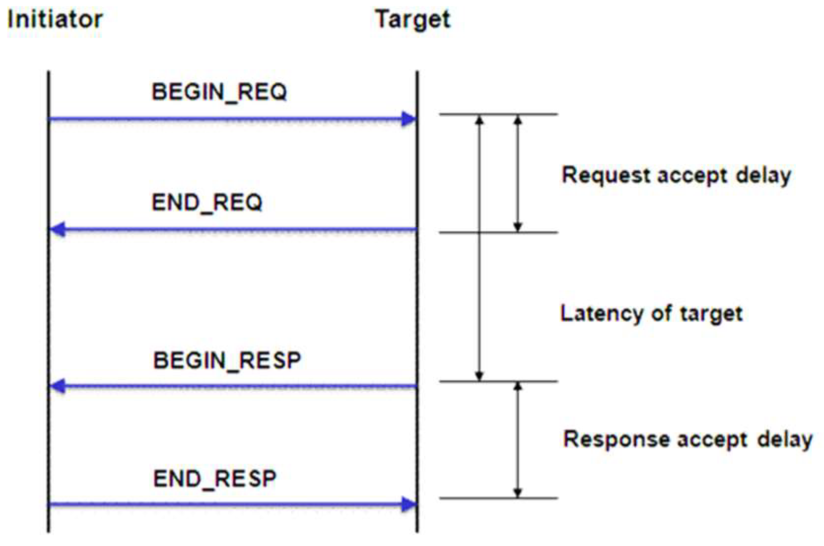
Communication between SystemC modules can be represented at the transaction level, with approximate timing information (TLM 2.0). We used the approximately-timed model, as shown in Figure 3. Two non-blocking calls are used, one for each communication direction. There must be no transaction within the two calls involving the progress of time, only logical and/or management operations can be performed. Each communication takes place in four phases: the start and the end of the request; the start and the end of the response.
The approximately-timed model has been chosen to better shape the communication among the different blocks of the controller. A parametric benchmark model has been created to replicate the traffic generated by a musical instrument and to drive the architectural exploration looking for the optimal configuration.
The System Level description of the NAND presented in this work does not consider all the low level details, and the time delay is just a parameter that can be modified by the user. Furthermore, the TLM description allows the abstraction from the specific signals used to send commands to the memory. For example, the TLM description using events is able to consider in the same way a read on a SDR (not including clock) and on a NV-DDR (including clock).
As an example, the architecture used to describe the management of the memory is the following. A Boolean variable is used to store the ready/busy status of the resource, which by default is considered ready. When the State Machine decides that an operation must be started, on the basis of the command sent, it performs the following operations:
- Verifies that the resource is not currently in use by a type variable bool managed by the resource thread
- Sets the time required to explicate the operation using a variable of type sc_time
- Notifies the thread of the start of the operation using the notify method of a sc_event variable
- Waits for a new event, moving to an appropriate state
When a command is executed, for example “Block Erase Interleaved”, the details of the signals involved are not considered. The proposed model could be used in principle either for ONFi 1.0 or for ONFi 4.1, extending the State Machine to all the possible commands. The commands implemented in ONFi 1.0 are 22 (mainly read, write, and erase operation), 34 in ONFi 4.0, and 39 in ONFi 4.1. Many of the additional commands are related to low level operations; for example, the ZQ CALIBRATION LONG (ZQCL) command is used to perform the initial calibration during a power-up initialization or reset sequence. Those commands have no meaning in a high level TLM description.
In this work, we want to investigate the optimal architecture using the interleaving and multi-channel techniques, aspects that are common to all the versions of the ONFi standard, therefore the results are general enough, even if the ONFi implemented is the 1.0.
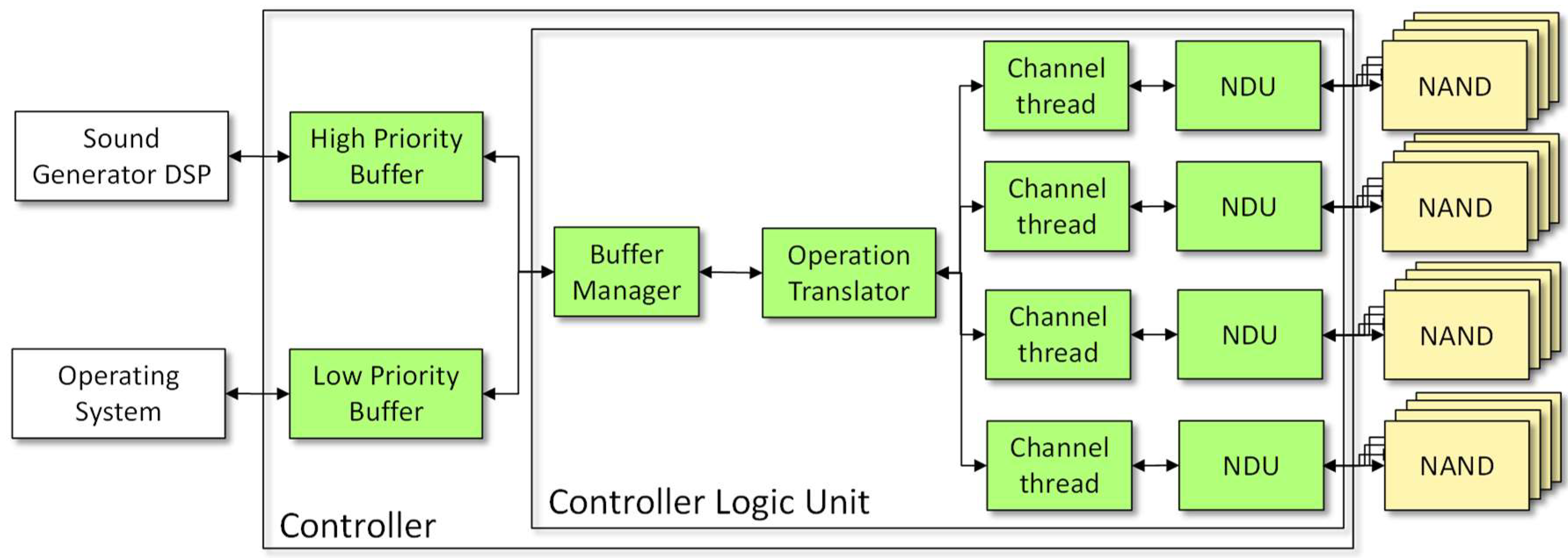
The architecture of the memory controller is described in Figure 4. The coexistence of two actors, the sound generation and the operating system, implies the need for a priority management logic to ensure in any case the performance of the audio real-time engine. For this purpose, a complete dual-host memory controller model has been developed. The architecture consists in the following main blocks:
- two buffers: a high-priority buffer (HP) is used to serve the low-latency real-time tasks and a low-priority buffer (LP) is assigned to operating system tasks with less strict latency and bandwidth constraints.
- Controller Logic Unit (CLU) is responsible for managing the priorities of the requested operations and the translation of these into simple tasks to be committed to NAND memories; it is the logical unit used to manage the multi-channel implementation.
- NAND Driver Unit (NDU) able to handle simultaneously multiple NAND flash chips connected to the same bus. This structure allows the interleaving of operations. The memory bank is abstracted as a unique memory with size equal to the sum of all memories capacity.
- NAND memory model, that is compliant with a real device specification.
4.1. Control Logic Unit Model
The CLU is responsible for the management of operation buffers and communication channels. The multi-channel technique is implemented. The CLU is composed of these entities:
- Buffer Manager. It picks up the requests from the buffers following a priority policy. All tasks are parsed, possibly aggregated, and passed to the address translator. Two different priority strategies have been provided in the model and their performances are tested:
- absolute priority: when the high-priority buffer sends a request, its operation is immediately served and the low-priority tasks are interrupted.
- parametric priority: at the end of the served request, the next processed task will be selected on the basis of a random number generator. The next task will belong to the high-priority buffer with a probability α, and to the high-priority buffer with a probability 1-α. The parameter α is fixed by the designer. The processes are not interrupted and they are brought to completion.
- Operation translator. It translates every request into requests for the single NDUs and it reassembles at the end of the operations. Furthermore, it manages the mapping from logical addresses to physical NDU addresses.
- Channel thread. A dedicated thread for each channel ensures the parallelism of the multi-channel management. Each channel thread communicates directly with the related NDU interface.
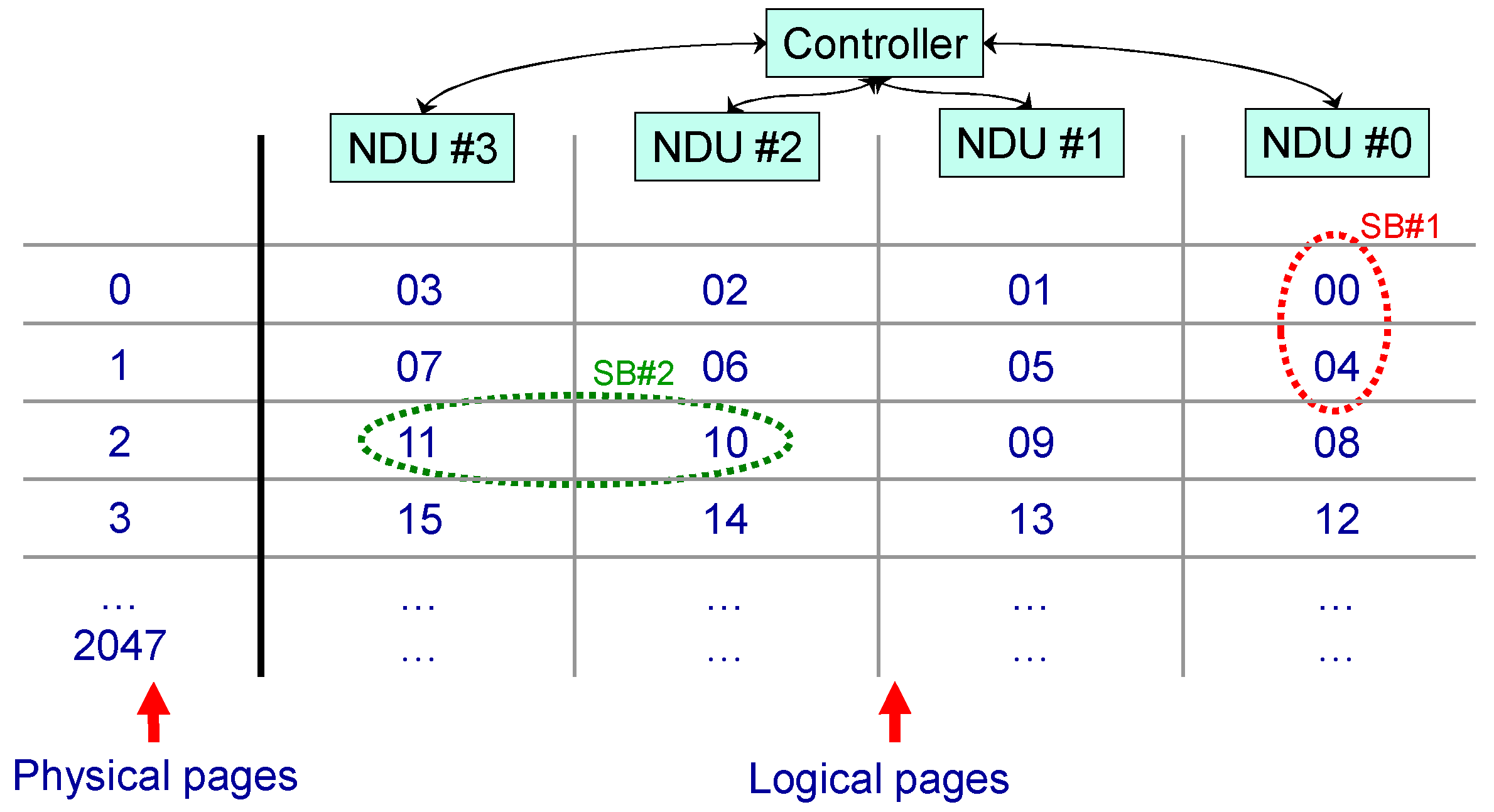
The address translator takes care of the multi-channel implementation, it also translates the logical operations in transactions for the NDUs connected to the different channels and vice versa. In this phase, the addressing of the memory is decided, as shown in Figure 5: the logical page number 5, for example, is located in page 1 of driver #1, and so on.
Furthermore, the audio samples are supposed to be organized in consecutive chunks of data constituted by a certain number of NAND memory pages. In this way, if the probability to access a particular address is uniformly distributed, on average a larger number of controllers will be used simultaneously, thus maximizing parallelism and therefore performance. In cases of inhomogeneous balancing of the various channels or when a request involves a single logical page, throughput is reduced and the multi-channel becomes less effective.
For these reasons, considering for example the situation reported in Figure 5, the reading of the streaming block #2 is performed faster than the reading of streaming block #1:
- streaming block #1: the memory controller must wait for the reading of two memory pages in order to complete the entire operation.
- streaming block #2: two controllers can be used to access two different memory pages at the same time.
4.2. NAND Driver Unit Model
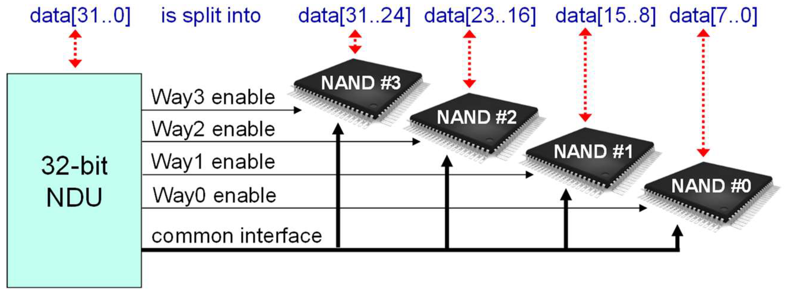
The NAND driver unit is a module that, via a single communication bus, is capable of driving multiple memories at the same time using the interleaving mechanism. The NDU is connected to multiple instances of the NAND memory and uses the ONFiprotocol to simulate the reading and writing of data. The organization of data within an NDU is carried out for individual pages as in the NAND memories. The data word size varies depending on the number of connected memories. Figure 6 reports, as an example, four memories for each NDU, the NDU page is characterized by 2048 words at 32-bit each. Therefore, each operation involves all the memories connected to the NDU, it is not possible to operate only on some of them. In this way it is possible to optimize the performance by fully exploiting the interleaving technique.
The NDU model is composed of the following entities:
- NDU interface: interface used by a host to request the execution of an operation.
- sub-driver: closely related to only one of the memories connected to the NDU. It takes care of completing the read or write operations to be performed on the specified set of memory pages. Each sub-driver communicates with its memory using a TLM interface operated by a shared I/O bus.
- I/O bus: it is managed through a FIFO buffer of input/output operations and it is executed on a dedicated thread. Whenever a sub-driver or a memory needs to access the bus, the related request is placed in the buffer.
- TLM interface: dedicated to the link with the NAND flash. It is a “multi-socket tagged” interface that is able to discriminate the communication channels of the different memory chip.
The samples in each NAND memory are placed in contiguous areas within the flash array. So, in most cases, each streaming block is written exactly in correspondence of consecutive logical pages and these are evenly distributed on all channels exploiting the maximum level of parallelism. This solution requires that the audio sample’s structure is not modified by any data-moving strategy, for example during wear-leveling or ECC management.
4.3. NAND Flash Memory Model
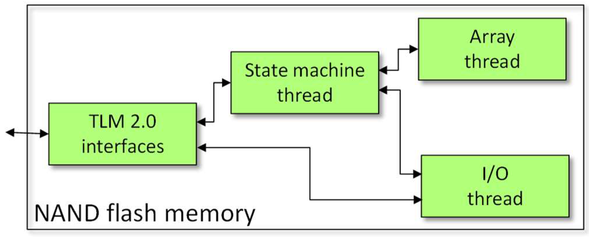
The SystemC model of the NAND consists of the following blocks, as shown in Figure 7:
- a specific thread implementing the finite state machine of the ONFi protocol. It takes new events from an incoming FIFO queue appropriately filled both by the TLM interface, and by the resource threads, each whenever a new event is to be communicated to the state machine.
- the io_wait_thread: an SC_THREAD that models the I/O bus through one Boolean state ready/busy and a timer that is driven by the state machine when the I/O for a certain amount of time.
- the array_wait_thread: an SC_THREAD that models the use of the array in a way similar to the I/O bus.
The Flash memory model takes care of reproducing the data storage and the exact timing of a real memory, but it does not address the management of possible errors in reading or writing operations, the error correction, and the deterioration of the charge inside the cells. The model also assumes that the operations always involve reading and writing one or more full pages.
The approximately-timed approach was adopted in order to achieve an acceptable model accuracy and simulation speed. Each communication is initiated by the NDU that requests a read, write, or delete operation. The request phase is represented by the input to the memory. The duration of this transaction is decided according to the memory timing parameters. The response phase is represented by the output where the host withdraws the data from the NAND. The duration of this transaction is determined by the host itself. The time between a request and a response transaction depends on internal flash array operations.
This level of detail in the modeling of timing and operations allows the controller to handle multiple memories simultaneously, whether they are connected to different buses or they share the same bus. At the end of the request of a particular operation it is possible to perform other tasks while waiting for the completion of the ongoing operation.
The model also provides for the storage of data in order to correctly simulate read, write, and erase operations involving possibly different memories.
The purpose of the SystemC model is to implement the executable specification of a real memory taken as a reference and provided also with a Verilog description. The two models were simulated and compared by running the same benchmarks. A careful refinement of the system-level model allowed it to avoid any significant timing mismatch between the low level Verilog description and TLM SystemC description.
The SystemC simulation turned out to be ~6600 times faster than the Verilog simulation.
5. Interleaving and Multi-Channel Techniques
In this work, we investigate, analyzing all the possible controller configurations, the optimal architecture to achieve the best performance, while maintaining reduced costs and design complexity.
Many features of the memory controller can be optimized: garbage collection wear leveling, bad block management, error correction, interleaving, and multi-channel. The results reported in the literature show that interleaving and multi-channel are the main techniques to improve data throughput.
The results reported in [4,5] show that pipeling and interliving, and exploiting inter-request parallelism allow an increment up to four times in the data throughput.
The results in [9] show that different FTL schemes and garbage collection algorithms have different impact on the power consumption of the NAND memory, but their impact on memory response time and throughput is limited.
Hu et al. in [12] investigated the effect of garbage collection and wear leveling policies on write amplification. They verified that wear leveling is a key to achieving high endurance, but it contributes only marginally to write amplification as compared with garbage collection.
The impact of software management algorithms such as garbage collection and wear leveling has also been studied in [13]. The results show that execution time becomes marginal and does not affect the overall bandwidth.
Therefore, in this work we focus on the optimization of interleaving and multi-channel techniques to the specific application of high quality sound generation. Interleaving and multi-channel can be used simultaneously, thus originating a high number of selectable combinations, so it is important to deeply understand features and drawbacks of each technique.
The interleaving technique is a way to share the same physical interface among multiple NAND memories. This approach is exploitable because, regarding the whole time required for the different operations, the I/O interface is busy only for a limited period and the controller simply must wait for the current task to be completed before performing a new one.
The characteristics of the NAND flash memory we considered as a reference are: standard ONFi 1.0, 8-bit word size, 50 MHz I/O interface, 2048 B page size, 25 µs page read, 200 µs page program, 700 µs block erase block. The ratio between the busy time of the interface and the period of the entire task is approximately 20% for write operations and about 80% for read operations.
The interleaving technique can be used to greatly increase the data write throughput, up to four times, while the reading speed is almost unaffected by this approach. The possibility to share the same interface across multiple NAND memories of course allows it to reduce the complexity of the controller and the physical area reserved to data/control buses wiring.
The minimum size of a readable or writable block of data is directly proportional to the number of interleaved memories; this aspect can have an influence on small operations and therefore on the performance in terms of IOPS. In the case of a real-time musical instrument, this aspect is closely linked to the size of the streaming-block and must be evaluated carefully.
The multi-channel technique can be used to parallelize operations on multiple memory banks by driving each of them with an ad-hoc controller and its own dedicated interface. These controllers must be managed by a logic unit that handles data traffic and address mapping. The main advantage of this technique lies in the fact that the performance increases linearly with the number of channels both for reading and write operations, allowing it to achieve very high performance. The main drawback is the increased complexity regarding the project of the controller unit and the connection with the memories.
It is possible to get very good results by combining the two techniques on the basis of the specific application requirements. In our particular application, a considerable data read throughput is required and, on the other hand, a modest data write performance is necessary. Once the target is reached for data read traffic with the minimum number of channels, it is convenient to increase the level of interleaving to improve data write throughput, confining complexity and cost, rather than to increase the level of multi-channel.
A crucial aspect regarding the use of interleaving and multichannel is memory pages address mapping strategy and its relationship with the type of traffic generated by the application. An unwise choice in this sense can lead to an inefficient use of multi-channel or the cancellation of the advantages of interleaving with significant consequences on the whole system performance.
6. Simulations Results
We developed a benchmark to test and to measure the performance of the desired memory controller configurations. Two threads are used to simulate the two hosts: the sound generator DSP and the operating systems, indicated in Figure 4. The two threads are traffic generators, generating randomly memory requests on the basis of the following parameters:
- throughput: the average throughput expressed in megabytes per second;
- type of transaction: it is used to specify a read, write, or erase task;
- request size: it is the payload, expressed in kilobytes, associated to each operation request;
- total size: it represents the entire simulation payload, expressed in megabytes; when this level is reached the host simulator stops its execution.
Before starting each simulation all the parameters discussed so far must be set:
- high- and low-priority hosts traffic configuration;
- number of NDU;
- number of memory chips connected to each NDU;
- priority strategy;
- high- and low-priority buffers dimension.
During the simulation, a log file is generated containing the temporal evolution of some important variables:
- buffers occupation expressed in kilobytes;
- waiting time, expressed in microseconds, of the oldest operation in the buffers;
- current processing channel: 0 = none, 1 = low-priority host, 2 = high-priority host.
The latency time is one of the performances considered: when a processing is completed the value the time the host had to wait before that specific request was served is stored. Therefore, considering the maximum waiting time, it is possible to verify if the chosen configuration for the controller has been effective in keeping the latency below the specified value. It is also very important to examine the occupation of the buffers: if it reaches saturation the controller cannot keep up any more with the host’s requests.
The controller configurations to be identified are those that meet the following minimum requirements of the sound generation described in Section 3:
- streaming block size: 16 KB
- number of voices: 256
- streaming block playback duration: 85 ms
- high-priority average read throughput: 48 MB/s
- low-priority average write throughput: 2 MB/s or 5 MB/s or 10 MB/s.
The traffic generations used in the simulations consists of 256 separate data requests each with a payload of 16 KB for the high-priority channel and 512 KB requests for the low-priority channel. The notation “N × M” in the structure of the controller indicates the number N of NDUs used (i.e., the multi-channel level) and the number M of NAND memory chips (i.e., the interleaving level) connected to each NDU.
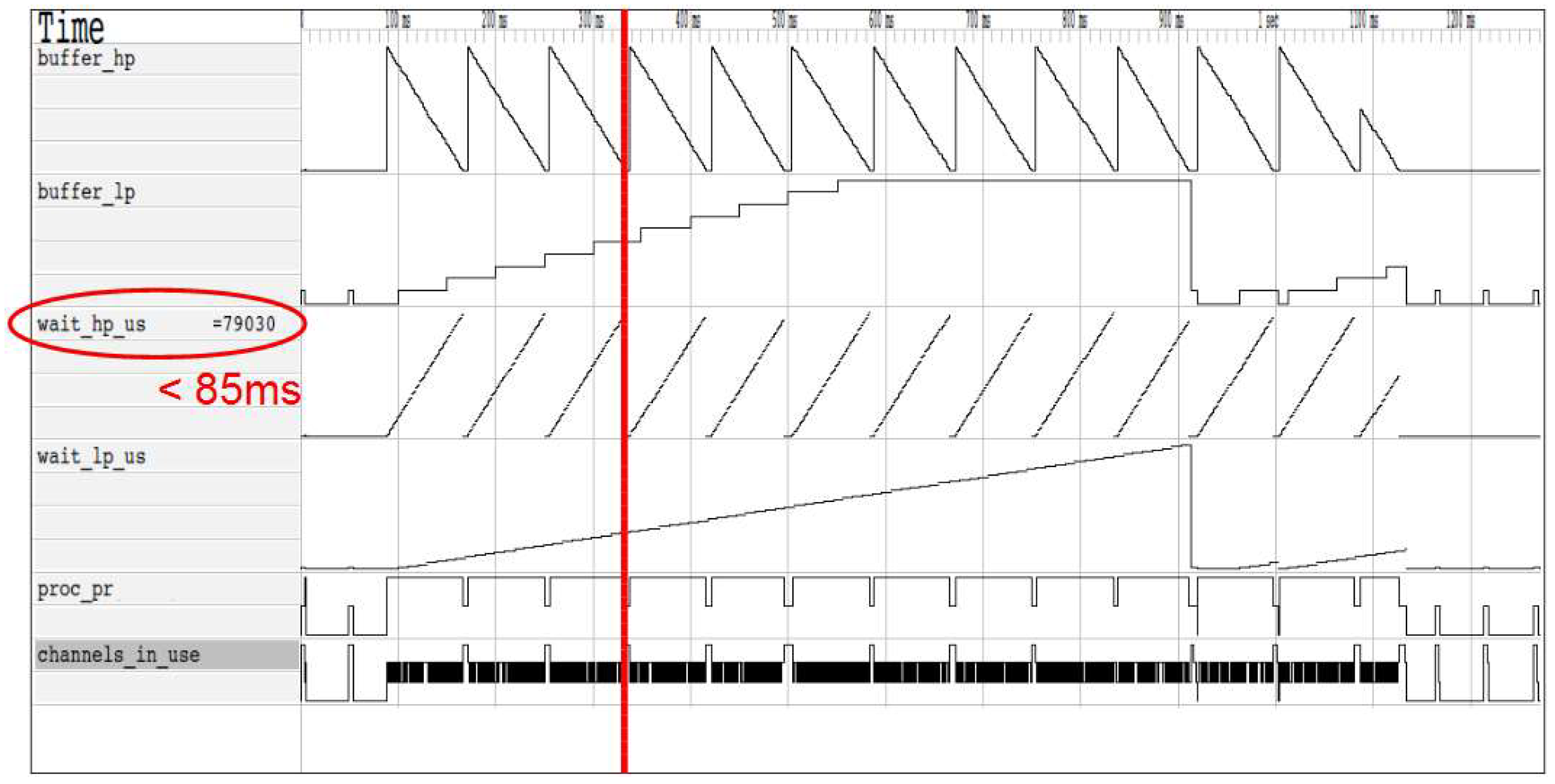
The results of a simulation for a “4 × 4” controller, with 4 NDUs and a total number of 16 NAND memories, are reported as an example. Figure 8 shows the values of some variables during a simulation. It is possible to note how the controller handles the different priorities of the buffers: a low-priority transaction is served only when the high-priority buffer becomes empty. For this particular simulation, the high-priority channel performance can be satisfied: the latency is approximately 79 ms, less than the required 85 ms.
The temporal variability observed from the graph is due to the fact that the traffic generated by the host uses random addresses and therefore, according to the distribution of the pages in the different memories, the performance level is not constant.
6.1. Performance Dependence on Different Levels of Multi-Channel and Interleaving
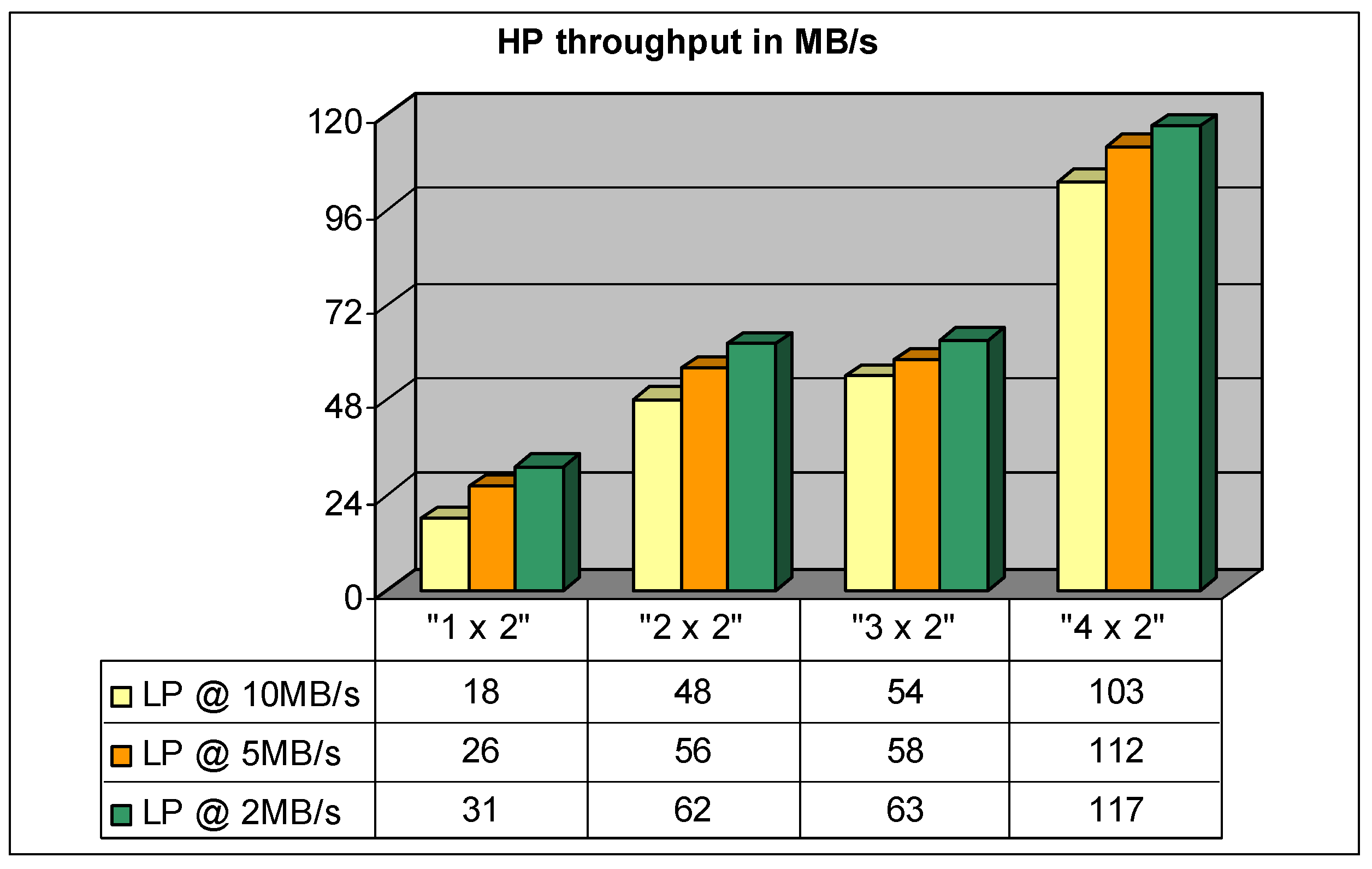
A set of 12 different controller configurations has been simulated, using the aforementioned data traffic generation. The results are reported in Figure 9, Figure 10 and Figure 11.
Figure 9 reports the high priority throughput for simulations regarding pure multi-channel configurations for the memory controller; all NDUs are connected to a single NAND memory chip. At a given value for the LP throughput the HP throughput grows linearly with the increase of the number of channels. In this case a good setup that satisfies all performance requirements is represented by the “2 × 1” configuration, which is able to provide 48 MB/s for the 256-voice sound generation process and 5 MB/s for the write tasks of the operating system. Using configurations with a higher number of channels, it is possible to reach a higher level of performance.
These configurations can be used to increase the polyphony of the instrument or to provide a higher memory bandwidth for other system services.
If the HP channel throughput is supposed to be set to a desired value, an increase in the level of interleaving generally causes an increase in the LP channel throughput. In this case the best compromise between performance and cost is represented by the “2 × 2” setup. To better understand the trend of the numeric results of Figure 9, Figure 10 and Figure 11, it is important to consider that for these configurations the NDU logical page is represented by 2048 words, each word is 16-bit wide for a total of 4 KB; i.e., two physical NAND memory pages. For every streaming block size of 16 KB the controller has to read four logical pages, the read performance is heavily affected by the dislocation of these pages among different channels:
- “1 × 2” configuration: the four logical pages are placed in the only possible NDU, the controller has to wait for the time equivalent to eight NAND page read operations (using the cache register), to complete the task.
- “2 × 2” configuration: the four logical pages are uniformly distributed in the two NDUs so the controller has to wait for half the time required in the previous case.
- “3 × 2” configuration: the four logical pages are placed in the three NDUs, but one NDU must be used to access two logical pages, as in the previous case; this is why the performance is similar to that of the “2 × 2” configuration.
- “4 × 2” configuration: the four logical pages are uniformly distributed in the four NDUs; all channels can be used simultaneously resulting in the best performance level.
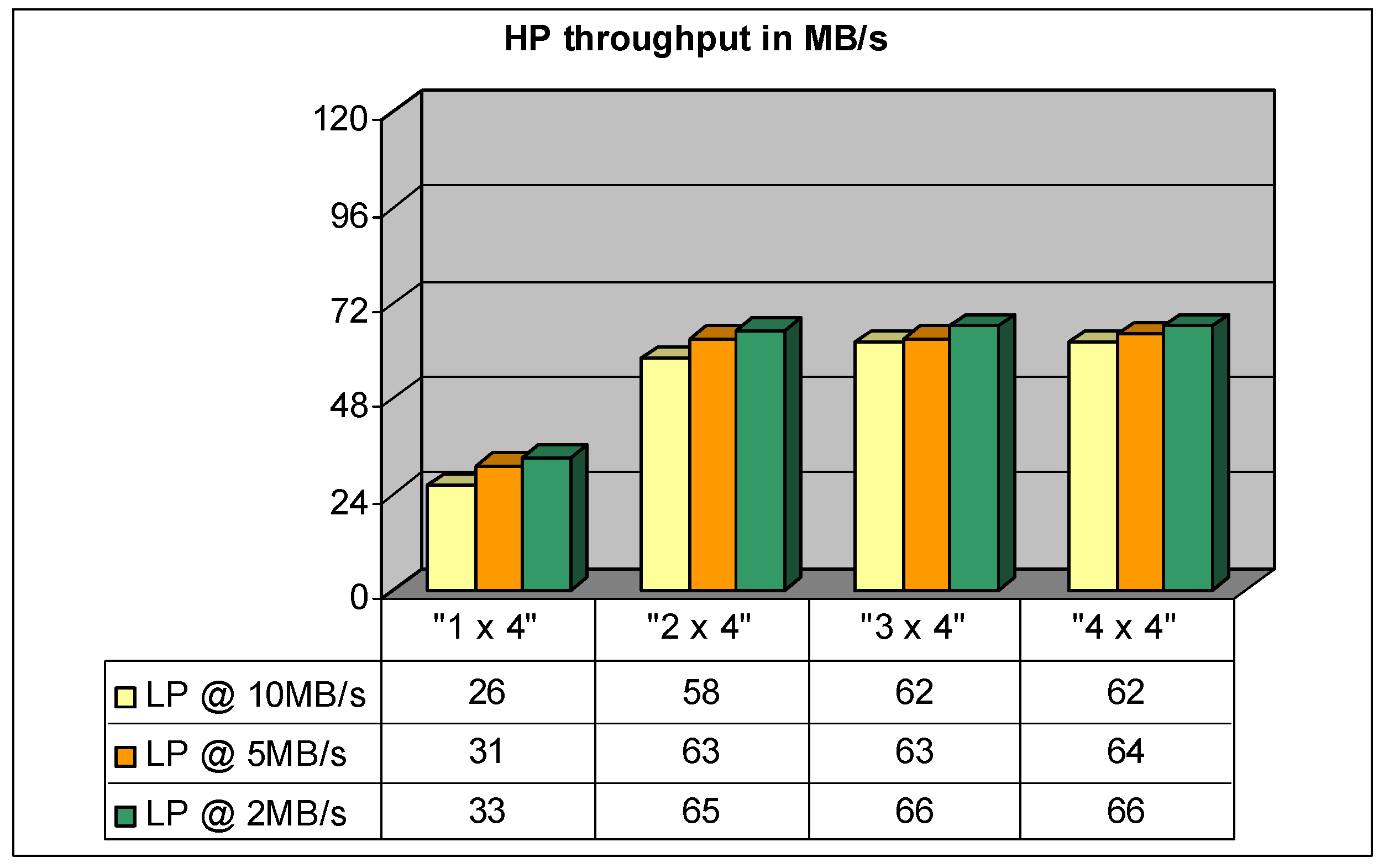
Figure 11 reports the results for simulations regarding configurations with the highest level of interleaving. In this case the NDUs are connected to four NAND memory chips and the logical page is represented by 2048 words, each word is 32-bit wide for a total of 8 KB; i.e., four physical NAND memory pages. For every streaming block two logical pages must be read.
For the same reasons explained for the “1 × 2” configuration, the “1 × 4” setup is the most unfavorable. On the other hand, increasing the number of channels from two to four doesn’t have a great impact on the read performance level because in any case only two channels can be used simultaneously to access the two uniformly distributed logical pages.
In general, a higher level of interleaving can be more efficiently used for a streaming block having a bigger size with respect to the logical page size, to maximize the use of all available channels.
6.2. Performance Dependence on the Streaming Block Size
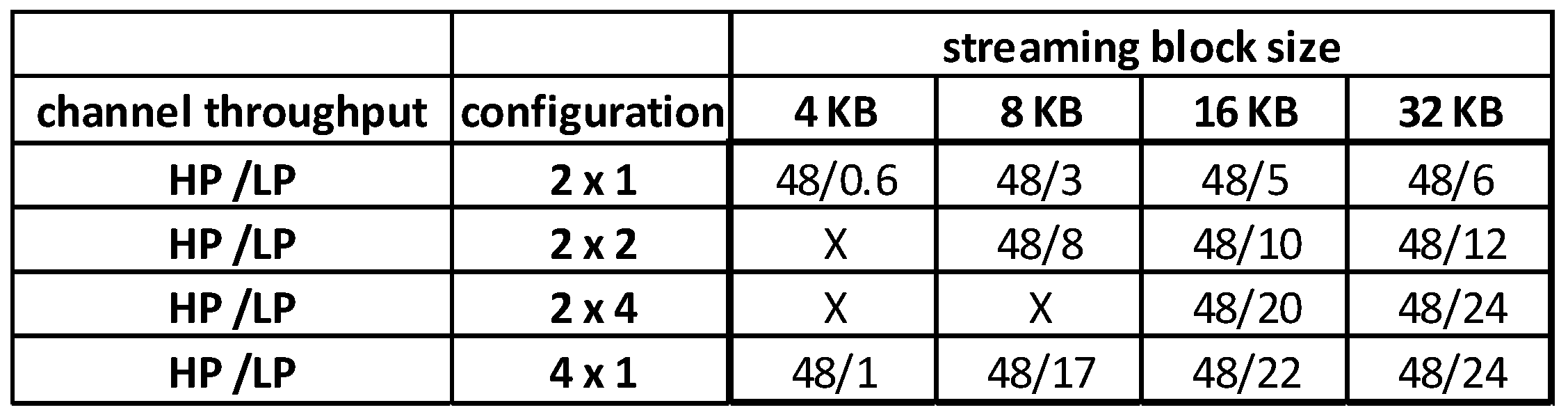
As a second analysis, we studied the dependence of performance on the size of the streaming block values of 4 KB, 8 KB, 16 KB, and 32 KB.
The dimension of a block affects these important parameters: playback time of the block itself, the amount of necessary SDRAM memory, and the startup time of the instrument.
The amount of SDRAM needed depends on the number of voices and on the total number of sounds stored in the instrument. As mentioned before, the streaming engine stores in the SDRAM the first block of every possible primary sound (up to 32,000) to be able to play it back instantly as soon as it is necessary. With a streaming block size of 16 KB, the SDRAM memory requirement is approximately 500 MB and it varies proportionally to the block size.
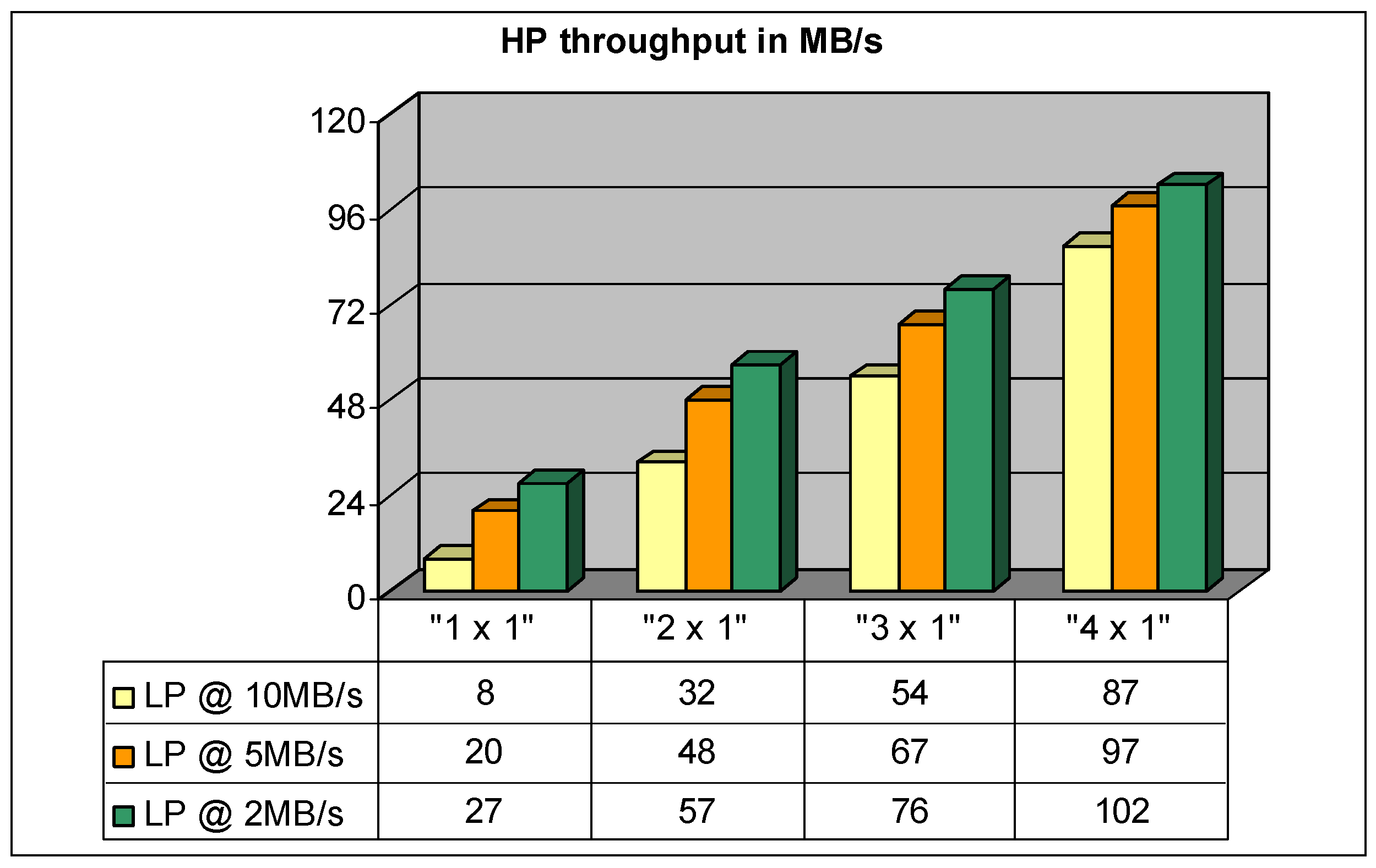
The average throughput required for the streaming to the memory controller in any case is equal to approximately 48 MB/s, but the frequency and the size of the requests change accordingly to the streaming block size. Increasing the block size, the memory works with larger, less frequent requests and the controller reaches higher performances. In the opposite case, the requests become smaller, more frequent and it is not possible to take advantage of the controller’s structure. Figure 12 shows the HP and LP channel throughput with different configurations and different size of the streaming block.
In the case of 4KB streaming blocks, the only possible configurations are those with at least two channels, “2 × 1” or “4 × 1”, without interleaving; nevertheless, the throughput of the low-priority channel drops down to 1 MB/s because of the heavy traffic generated on the high-priority channel. Therefore this scheme can be used only in the absence of a low-priority host or in the event that this generates extremely light traffic.
The “2 × 2” controller setup is able to also handle the smaller 8 KB streaming block size, but the LP bandwidth is limited to only 8 MB/s because of the reduced level of interleaving. An alternative scheme must be used if a higher performance level is needed. The idea is to use four NDUs without any interleaving, “4 × 1” configuration, so that the logical page has a size of 2 KB and each block is provided in the time of a single physical page read operation. The throughput of the low-priority host can reach up to 17 MB/s. For this solution the SDRAM quantity needed is around 250 MB.
Using larger streaming blocks means having more time to serve them and getting the best advantages from cache reading operations and other possible optimizations. Since the average throughput required by the streaming engine is constant, using 32 KB blocks the controller is able to get better performances from the NAND memories, leaving greater execution time to the low-priority host. The best configuration also in this case is “2 × 2” that allows to increase the performance in the low-priority channel up to 12 MB/s. In any case, this solution does not offer enough benefits to justify a doubling of the SDRAM memory used by the streaming engine that in this case is approximately 1 GB.
7. Conclusions
In this work we used the system level TLM modeling methodology in SystemC. The TLM design flow turned out to be very effective for architecture exploration and performance analysis. System exploration can be easily performed by means of fast and accurate simulation with abstracted transactions. The study and design of the controller for real-time music applications led to an implementation scheme that is able to satisfy all the predefined specifications and reaching a limited complexity level. Depending on the desired performance some excellent solutions can identified to allow the execution of a polyphonic audio streaming engine using high-quality samples; furthermore, the necessary bandwidth performances are guaranteed for the operating system in the access to the nonvolatile memory.
Author Contributions
Investigation, A.R.; Methodology, M.C., M.C. and F.R.; Software, M.G. The authors equally contributed in the work presented in the paper.
Funding
This research received no external funding.
Conflicts of Interest
The authors declare no conflict of interest.
References
- Kim, D.; Bang, K.; Ha, S.H.; Yoon, S.; Chung, E.Y. Architecture Exploration of High-Performance PCs with a Solid-State Disk. IEEE Trans. Comput. 2010, 59, 878–890. [Google Scholar] [CrossRef]
- Ou, Y.; Xiao, N.; Lai, M. A Scalable Multi-channel Parallel NAND Flash Memory Controller Architecture. In Proceedings of the Sixth Annual Chinagrid Conference ChinaGrid, Liaoning, China, 22–23 August 2011; pp. 48–53. [Google Scholar]
- Open NAND Flash Interface Specification. Available online: http://www.onfi.org/specifications (accessed on 16 May 2018).
- Kang, J.U.; Kim, J.S.; Park, C.; Park, H.; Lee, J. A multi-channel architecture for high-performance NAND flash-based storage system. J. Syst. Archit. 2007, 53, 644–658. [Google Scholar] [CrossRef]
- Micheloni, R.; Marelli, A.; Commodaro, S. NAND overview: From memory to systems. In Inside NAND Flash Memories; Micheloni, R., Crippa, L., Marelli, A., Eds.; Springer: Dordrecht, The Netherlands, 2010; Chapter 2; pp. 19–53. [Google Scholar]
- Kim, S.; Park, C.; Ha, S. Architecture Exploration of NAND Flash-based Multimedia Card. In Proceedings of the Design, Automation and Test in Europe, Munich, Germany, 10–14 March 2008; pp. 218–223. [Google Scholar]
- Jose, S.T.; Pradeep, C. Design of a multichannel NAND Flash memory controller for efficient utilization of bandwidth in SSDs. In Proceedings of the 2013 International Multi-Conference on Automation, Computing, Communication, Control and Compressed Sensing, Kottayam, India, 22–23 March 2013; pp. 235–239. [Google Scholar]
- Chang, Y.H.; Lu, W.L.; Huang, P.C.; Lee, L.J.; Kuo, T.W. An Efficient FTL Design for Multi-chipped Solid-State Drives. In Proceedings of the International Conference on Embedded and Real-Time Computing Systems and Applications, Macau, China, 23–25 August 2010; pp. 237–246. [Google Scholar]
- Kim, Y.; Tauras, B.; Gupta, A.; Urgaonkar, B. FlashSim: A simulator for NAND flash-based solid-state drives. In Proceedings of the 2009 First International Conference on Advances in System Simulation, Porto, Portugal, 20–25 September 2009; pp. 125–131. [Google Scholar]
- Lee, J.; Byun, E.; Park, H.; Choi, J.; Lee, D.; Noh, S.H. CPS-SIM: Configurable and accurate clock precision solid state drive simulator. In Proceedings of the Annual ACM symposium on Applied Computing, Honolulu, HI, USA, 9–12 March 2009; pp. 318–325. [Google Scholar]
- Jung, H.; Jung, S.; Song, Y.H. Architecture exploration of flash memory storage controller through a cycle accurate profiling. IEEE Trans. Consum. Electron. 2011, 57, 1756–1764. [Google Scholar] [CrossRef]
- Hu, X.Y.; Eleftheriou, E.; Haas, R.; Iliadis, I.; Pletka, R. Write amplification analysis in flash-based solid state drives. In Proceedings of the SYSTOR ’09 Proceedings of SYSTOR 2009: The Israeli Experimental Systems Conference, Haifa, Israel, 4–6 May 2009. Article No. 10. [Google Scholar]
- Zuolo, L.; Zambelli, C.; Micheloni, R.; Indaco, M.; Di Carlo, S.; Prinetto, P.; Bertozzi, D.; Olivo, P. SSDExplorer: A Virtual Platform for Performance/Reliability-Oriented Fine-Grained Design Space Exploration of Solid State Drives. IEEE Trans. Comput.-Aided Des. 2015, 34, 1627–1638. [Google Scholar] [CrossRef]
- VS, J.C.; Brito, A.V.; Nascimento, T.P. Verification of Embedded System Designs through Hardware-Software Co-Simulation. Int. J. Inf. Electron. Eng. 2015, 5. [Google Scholar] [CrossRef]
- Giammarini, M.; Orcioni, S.; Conti, M. Powersim: Power estimation with SystemC: Computational complexity estimate of a DSR front-end compliant to ETSI Standard ES 202 212. In Solutions on Embedded Systems; Series: Lecture Notes in Electrical Engineering; Springer: Dordrecht, The Netherlands, 2011; Chapter 20; pp. 285–300. [Google Scholar]
- Kornaros, G.; Grammatikakis, M.D.; Coppola, M. Towards Full Virtualization of Heterogeneous NoC based Multicore Embedded Architectures. In Proceedings of the 2012 IEEE 15th International Conference on Computational Science and Engineering, Nicosia, Cyprus, 5–7 December 2012; pp. 345–352. [Google Scholar]
- Caldari, M.; Conti, M.; Coppola, M.; Curaba, S.; Pieralisi, L.; Turchetti, C. Transaction-Level Models for AMBA Bus Architecture Using SystemC 2.0. In Proceedings of the Design, Automation and Test in Europe, Muenchen, Germany, 3–7 March 2003; pp. 26–31. [Google Scholar]
- Vece, G.B.; Conti, M.; Orcioni, S. Transaction-level Power Analysis of VLSI Digital Systems. Integr. VLSI J. 2015, 50, 116–126. [Google Scholar] [CrossRef]
- Devi, D.R.; Kondugari, P.K.; Basavaraju, G.; Gangadharaiah, S.L. Efficient implementation of memory controllers and memories and virtual platform. In Proceedings of the International Conference on Communications and Signal Processing, Melmaruvathur, India, 3–5 April 2014; pp. 1645–1648. [Google Scholar]
- SystemC TLM (Transaction-Level Modeling) Working Group. Available online: http://accellera.org/activities/working-groups/systemc-tlm (accessed on 16 May 2018).
Figure 1.
Polyphony, arrangement, and pitch shifting to extend audio samples performed by the digital signal processor (DSP) using low latency memories.
Figure 1.
Polyphony, arrangement, and pitch shifting to extend audio samples performed by the digital signal processor (DSP) using low latency memories.

Figure 2.
ONFi standard revisions.

Figure 3.
Example of approximately-timed Transaction Level Modeling (TLM).

Figure 4.
Block diagram of the memory controller model.

Figure 5.
Samples arrangement and NAND Driver Unit (NDUs) pages mapping.

Figure 6.
Example of a 4-way (32-bit) NAND driver unit.

Figure 7.
NAND flash memory model.

Figure 8.
Waveforms of the different simulation parameters.

Figure 9.
Performance of “N × 1” configurations.

Figure 10.
Performance of “N × 2” configurations.

Figure 11.
Performance of “N × 4” configurations (fully interleaved NDUs).

Figure 12.
High-priority buffer (HP)/Low-priority buffer (LP) channel throughput with different configurations and different size of the streaming block.
Figure 12.
High-priority buffer (HP)/Low-priority buffer (LP) channel throughput with different configurations and different size of the streaming block.

© 2018 by the authors. Licensee MDPI, Basel, Switzerland. This article is an open access article distributed under the terms and conditions of the Creative Commons Attribution (CC BY) license (http://creativecommons.org/licenses/by/4.0/).
Share and Cite
MDPI and ACS Style
Conti, M.; Caldari, M.; Gianfelici, M.; Ricci, A.; Ripa, F. SystemC/TLM Controller for Efficient NAND Flash Management in Electronic Musical Instruments. Electronics 2018, 7, 75. https://doi.org/10.3390/electronics7050075
AMA Style
Conti M, Caldari M, Gianfelici M, Ricci A, Ripa F. SystemC/TLM Controller for Efficient NAND Flash Management in Electronic Musical Instruments. Electronics. 2018; 7(5):75. https://doi.org/10.3390/electronics7050075
Chicago/Turabian StyleConti, Massimo, Marco Caldari, Matteo Gianfelici, Adriana Ricci, and Franco Ripa. 2018. "SystemC/TLM Controller for Efficient NAND Flash Management in Electronic Musical Instruments" Electronics 7, no. 5: 75. https://doi.org/10.3390/electronics7050075
Note that from the first issue of 2016, this journal uses article numbers instead of page numbers. See further details here.