Multi-Port Current Source Inverter for Smart Microgrid Applications: A Cyber Physical Paradigm


School of Electrical Engineering, Vellore Institute of Technology, Chennai 600127, India
*
Author to whom correspondence should be addressed.
Electronics 2019, 8(1), 1; https://doi.org/10.3390/electronics8010001
Submission received: 19 October 2018
/
Revised: 29 November 2018
/
Accepted: 10 December 2018
/
Published: 20 December 2018
(This article belongs to the Special Issue Cyber-Physical Systems)
Abstract
:This paper presents a configuration of dual output single-phase current source inverter with six-switches for microgrid applications. The inverter is capable of delivering power to two independent set of loads of equal voltages or different voltages at the load end. The control strategy is based on integral sliding mode control (ISMC). The cyber twin model-based test bench is developed to analyze the performance of the inverter. The cyber twin is a virtual model of the physical system to simulate behaviours. The performance of the inverter is analyzed with a cyber twin model and monitored through the remote system. Also, the inverter is analyzed with different voltage conditions.
1. Introduction
The distributed generation (DG) with photovoltaic, wind energy, fuel cell, and battery, termed as microgrid, can supply for low- and medium-voltage applications. The DC microgrid is capable of supplying both DC loads and AC loads with the inverter. The inverters for microgrid discussed in [1,2] are capable of supplying a single output. The inverters with reduced semiconductor switches and dual output are capable of feeding dual loads and less complexity in implementation. This enables the feeding of different types of loads using an inverter. The development of inverter with reduced power semiconductor devices makes the system economical and compact. The dual output inverters reduce the number of switches in a system and supplies energy to two AC autonomous loads. A four-switch inverter [3] is initially proposed with the reduced number of switches by replacing split capacitors for sharing between power converters. The dual output voltage source inverters discussed by Yu, Strake et al. [4] are dual phase single DC bus inverter with four-switches, three wire single-phase inverter with six-switches, dual phase dual DC bus inverter with four-switch, dual phase with four-switch and transformer. The inverter models discussed in [4] has the capability of operating only in half bridge configuration. The dual output single-phase inverter based on voltage source inverters (VSI) is proposed by Fatemi, et al. [5] explains about the half-bridge dual output inverter with the split capacitor as a sharing leg for both outputs and for the full bridge dual output with six-switches; the switch leg is common of for both outputs by sharing a row of switches for upper and lower outputs. The six-switch voltage source inverter delivers equal voltage at the output with open loop operation. The six-switch dual output with buck structure delivers dual output with the equal voltage at both output and operated in open loop is presented by Nguyen, et al. [6]. The dual output inverter with sharing of switch legs will results in the reduction of semiconductor switches by .
From the literature, most of the researchers concentrate on dual output voltage source inverter rather than the dual output current source inverter. The current source inverters (CSI) have inherent short circuit protection owing to the presence of a dc link reactor which results in the low harmonic distortion and better load voltage regulations [7,8]. The control of CSI is difficult compared to VSI due to the simultaneous regulation of DC link current and output voltage. The dynamic response of CSI is studied using a current controller [9] and continuous time-based control strategy is employed [10]. The sliding mode control (SMC) [8,11,12] provides a dynamic response to the nonlinear systems with the property of hysteresis. It offers stability to variations in system parameters and easy implementations. The sliding surface is created with reference to error variable of inductor current and capacitor voltage for single-phase single output CSI is proposed by Komurcugil, et al. [13]. The sliding mode control for voltage source inverter-based shunt active filter is presented in [14] for power quality improvements in the power system. The control of y source boost DC–DC converter controlled by cascaded sliding mode control is proposed by Ahmadzadeh et al. [15]. The control of power electronics equipment using sliding mode control is presented in the various literature for multi-terminal HVDC [16], induction motor control [17], h6 inverter [18], and modular multilevel converter [19]. The SMC [20] based control strategies are applied widely to single output inverters [1,2] rather than dual output inverters from the literature. To implement continuous time-based control strategies processors with high-speed data processing is required. Reconfigurable Input/Output (RIO) based processors are utilized effectively for these types of controllers [21].
The interfacing of the power electronics circuits to the smart environment [22,23] makes the system more efficient and controllable. This provides two-way communication between the target and the users (man to machine and vice versa) and results in cyber–physical systems (CPS) [24]. The CPS implementation will result in smart grids [25,26,27] and remote laboratories for educational purposes. The definition of CPS given by E.A. Lee [28] is that the integration of physical process with embedded computation, controlling and network monitoring along with the feedback loops for computations. In another way, CPS is defined as a controllable, credible and scalable network with the physical system. The CPS is stated as (Computations, Communications, and Control). The basic concepts, method, and implementation of CPS is explained briefly by Liu, et al. [29]. CPS implementation for conveyor belt block pickup with application and platform level reconfiguration is in case of faults is presented by Andalam, et al. [30]. The CPS-based optimal power flow management in electric grid with energy demand management is proposed by Nguyen, et al. [31]. The remote monitoring of microgrid using LabVIEW and PLC has proposed in [32]. The researchers developed various CPS models for the physical systems with the utilization of wireless sensor network (WSN), radio frequency identification (RFID), Zigbee, CAN protocols [33,34,35,36,37]. The WSN can only sense signal but not capable of identifying the specific one from more sensors. Similarly, RFID also senses the data based on the perception of data. RFID is widely used in the Internet-of-Things (IoT). While IoT only has the perception of sensing alone, but CPS has the ability of the robust control to the target. The comparison of CPS for various applications is given in Table 1.
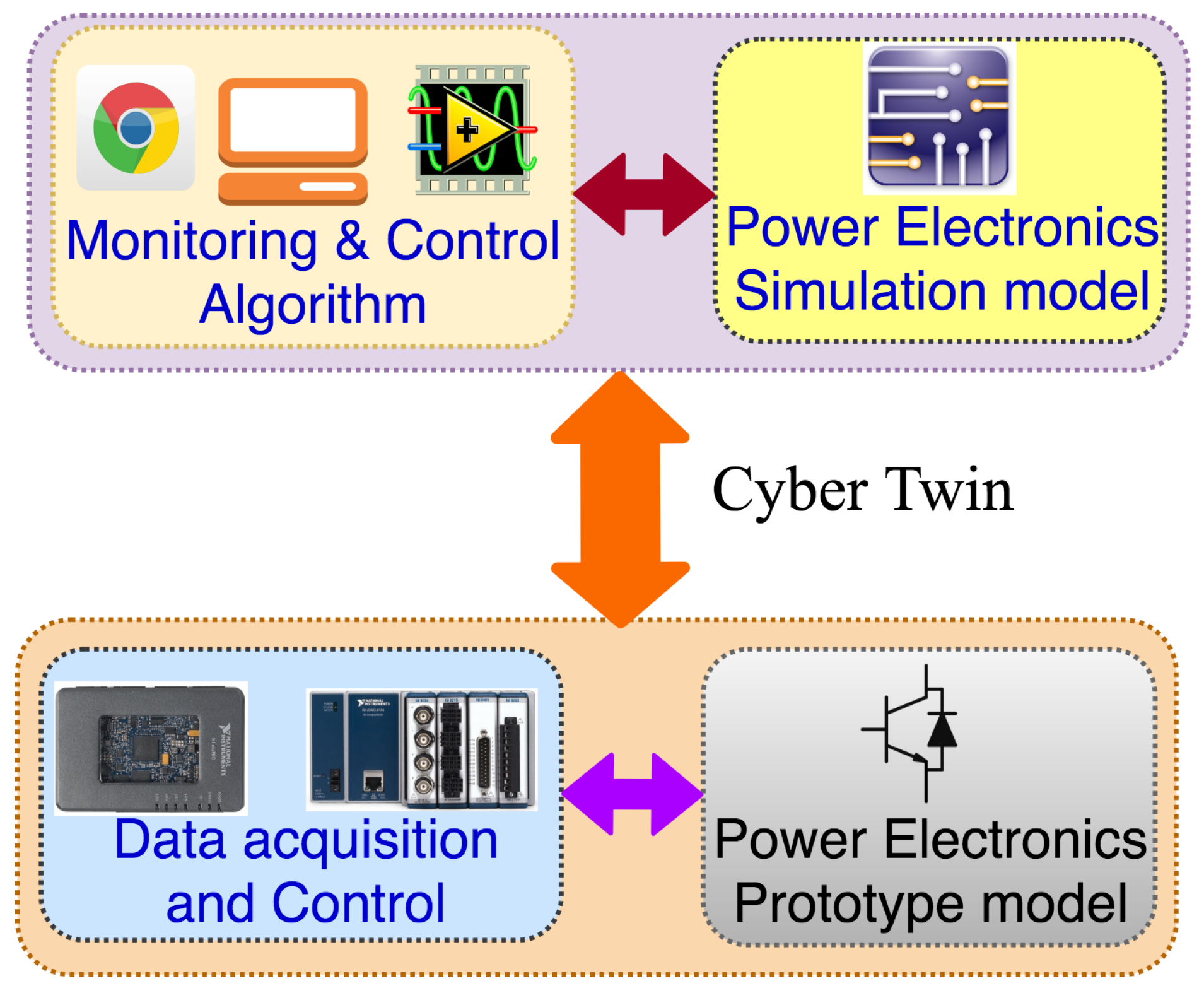
As the growth in the CPS, the cyber twin (digital twin) [38] approach is introduced to realize the behaviour of the physical system with a virtual model. In the cyber twin approach, a virtual model realizes the behaviour of the physical system to predict the dynamic changes and respond to the system for better operation. The cyber twin approach has been proposed by various researchers; Kazi et al. [39] proposed fuzzy-based vehicle CPS system for driving assistance. To increase the feasibility in furniture production line Hao Zhang et al. [40] introduced the cyber twin approach. The comparison of cyber twin and big data for Industry 4.0 is anticipated by Qinglin et al. [41] to identify the possibilities and advantages of cyber twin for Industry 4.0.
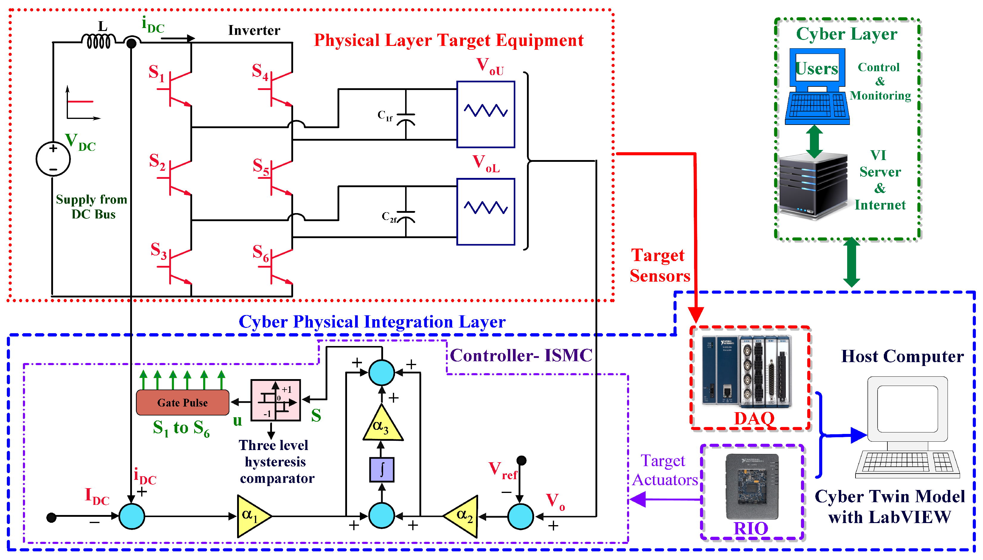
In this paper, the modeling of dual output current source inverter with the capability of operating in equal voltage and different voltage modes at the output end for microgrid applications. The sliding mode control (SMC) strategies are introduced to control the dual output inverter and performance analysis of sliding mode and integral sliding mode control (ISMC) is performed. The comparative analysis of SMC and ISMC reveal the performance and better controller for a dual output current source inverter. The main advantages of ISMC are robustness of large variations, stability, and fast dynamic response. The integration of power electronics devices and cyber–physical systems (CPS) is introduced. The cyber twin model of the inverter is developed with LabVIEW and Multisim packages. The cyber twin model is the virtual model of the physical system; it operates by sensing the raw data for the analysis and control of the physical system. The cyber–physical test bench is developed with cyber twin model of the inverter. In literature for implementing cyber–physical test bench utilizing multidomain programming is given in Table 1. To avoid the complexity by utilizing the multidomain program, LabVIEW based single domain programming is used. The integration of this heterogeneous frame is needed to deploy on the single platform to reduce the data exchange error which occurs while using a different platform for each section. The cyber–physical test bench is developed based on LabVIEW, MyRIO, C-DAQ and NI-Web services. The interaction of cyber twin model by cyber integration layer with the physical device is needed for effective control of the system. The performance of the physical device is monitored by web services.
2. A Cyber Perspective Model
The Reconfigurable Input/Output (RIO)-based design of cyber–physical system RCP evaluation test bench is created for the evaluation of two switch dual output inverter with ISMC control. The experimental setup consists of three sections Physical layer, cyber–physical integration layer, and cyber layer. The CPS architecture consists of three layers: Physical layer, cyber–physical integration layer, and Cyber layer. Physical layer comprises of the physical device (target) which needs to be controlled and monitored by CPS. The cyber–physical integration layer has the sensors, controllers and software technologies with a host computer to collect the data from the physical device and to control the device based on the responses. In this layer the integration of cyber twin with physical model is initiated.
Cyber twin approach for power electronics systems is introduced and with cyber infrastructure. The virtual model of the physical model is developed to simulate the real behaviour and analyze the system. The Figure 1 displays the block diagram of the proposed cyber twin approach. The virtual model is developed in LabVIEW-Multisim packages. The physical device (inverter) voltage and current are sensed through data acquisition and analyzed with the virtual model in the host computer.
The data observed from this layer is monitored and the physical device is controlled by the control center through the internet. The data transfer between the physical device and control center is executed by cyber layer. Figure 2 shows the configuration of the proposed RCP evaluation of the inverter.
Generalised CPS Model
The physical layer consists of the devices which are needed to monitor and control through CPS. Here the physical layer considered is inverter prototype with source and load. The generalised physical model is represented by Mulit-Input-Multi-Output (MIMO),
where, A is the system matrix, B is the input matrix, C is the output matrix, x(t) is the state vector, is the control vector, is the observation vector.cyber–physical integration layer makes the interconnection between the physical layer and cyber layer. The devices which employed for integration are voltage/current sensor, driver circuits with an optocoupler, data acquisition system, and host computer. The control structure is given by,
where, is the connection structure between controller and sensor. is non zero and shows the connection between controller () and sensor (j). The system with closed loop is given by,
The dynamics of the system with delay between sensor and controller is represented by,
The switching function of the system is given by,
To design the controller with the capabilities of cyber twin, the Sliding Mode Control (SMC) is identified due to modelling of control strategy based on mathematical model of the system.
3. Physical Layer: Dual Output Current Source Inverter
The microgrid schematic with proposed dual output inverter is shown in Figure 3. The proposed inverter is compared with the family of dual output inverters and given in Table 2. The configuration of the proposed dual output current source inverter is shown in Figure 2.
It consists of a DC link reactor with six semiconductor switches. The inverter has two legs with three semiconductor switches and a sharing row of switches for upper and lower output. The inverter is capable of operating at equal voltages (EV) and different voltages (DV).
3.1. Equal Voltage (EV) Mode of Operation
In this mode, the two AC outputs voltages are independent and equal. The inverter works similar to a full bridge with two parallel loads. The gate signals for upper () and lower () switches are generated by the control strategy. The control signals for sharing switches () is generated by the logical XOR of the upper and lower signals. The instantaneous output voltage () of the dual output inverter are same when it operates at EV mode is expressed in (10).
3.2. Different Voltage (DV) Mode of Operation
In this operating condition, the inverter is capable of delivering different voltage magnitude. The upper side will act as a full bridge and lower will act as a half bridge. The DV mode is in existence due to the presence of a DC link reactor. It will protect the inverter from short circuit and floating modes. If the inverter is operated at different voltage mode, the upper side voltage () will be in full bridge mode as expressed in Equation (11) and the lower side () will be in half bridge mode. The output equations for the half bridge are given by (11).
3.3. System Modelling
The dual output inverter is modeled based on CSI topology. It comprises the source voltage (), a DC link reactor (L), IGBT switches, output capacitive filter (C) and a resistive load (R). The equation of the CSI is written as,
where, u is the switching function, is the input DC voltage, is the output AC current, and the internal resistance of DC link reactor. In order to reduce the computational parameters of dual output inverter, it is assumed that as dual output capacitive filter and as the dual output voltage. The state space for the system operation is described in matrix form is given by (14),
The transfer function for the system operation is represented in (15),
4. Cyber–Physical Integration Layer: Cyber Twin Model, C-DAQ, RIO with Sliding Mode Controllers
Cyber–physical integration layer in a CPS incorporates the algorithm to gather sensor information and issue control signals through actuators to the physical device. This layer has software and hardware coordination in-order to control and monitor the physical device. The cyber twin model of the inverter is developed for the integration with the physical device. The CPS should behave as, (A) Intelligent: To predict and understand the behaviour of the system using LabVIEW environment, (B) Real-Time: To gather the real-time data from physical device C-DAQ-9174 is utilised, (C) Adaptive & Predictive control: To respond and anticipate the changes in the physical systems the ISMC based control strategy is implemented in MyRIO-1900.
4.1. Sliding Mode Control (SMC)
The Sliding Mode Control (SMC) is an effective controller with switching nature of inverter derived from the system model. The advantages of SMC are, it has a better dynamic response, stability against the variations of the load and easy implementation. It consists of inner and outer control loops. The input inductor current and output capacitor voltage is considered as the state variables for controlling. The error variables are given by,
The sliding surface (S) of SMC is expressed by (17),
where, and are the sliding coefficients. The additional variable accumulates directly to the steady-state errors of and . The time derivative of (17) is,
The derivatives of and is given by (19) and (20),
By substituting (19) and (20) in time derivative Equation (18) gives (21),
where A is given by (22),
The condition for stability should be satisfied and the control variable is given by,
To satisfy the stability condition, and is incorporated to Equation (21).
4.2. Integral Sliding Mode Control (ISMC)
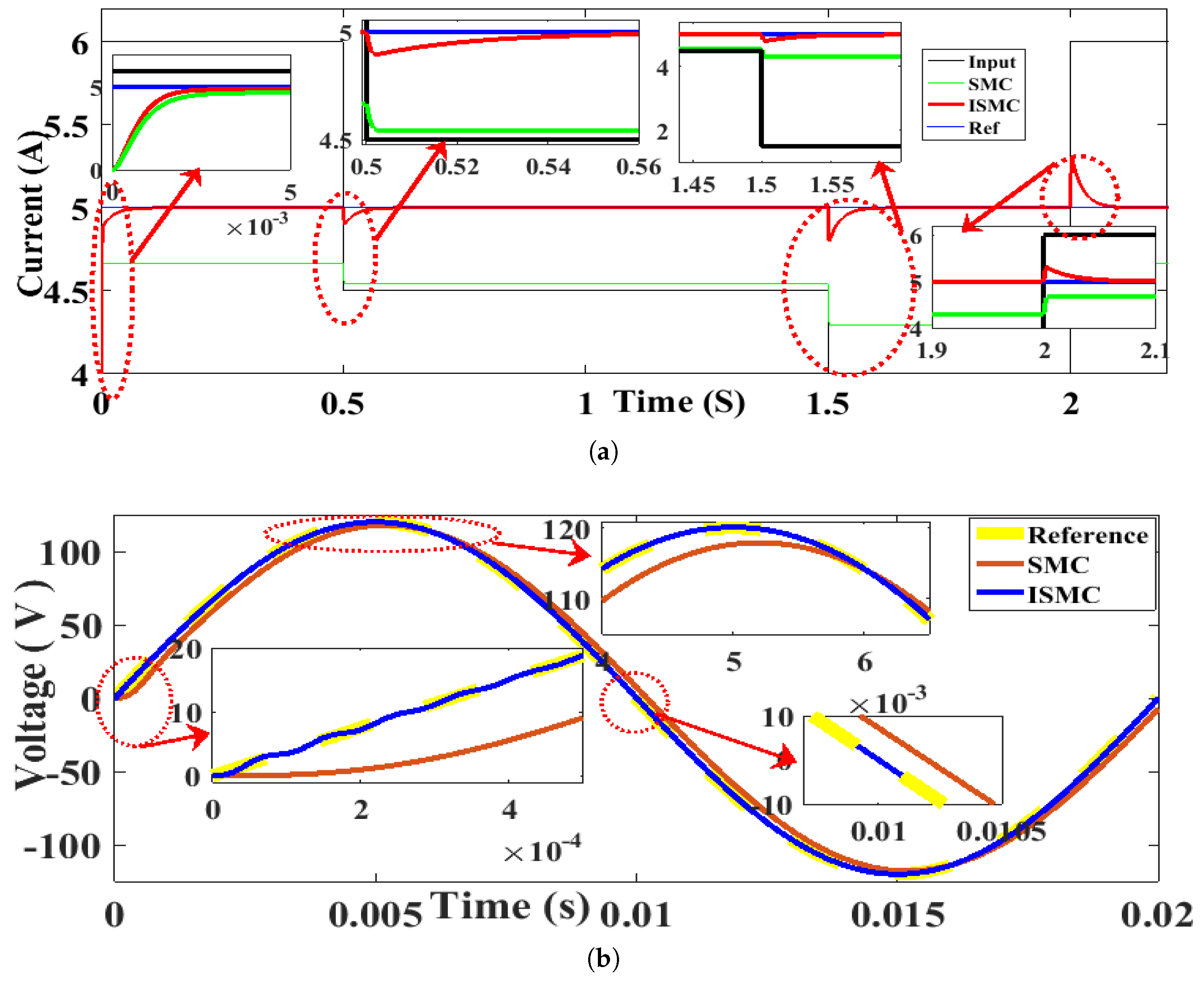
The SMC-based control has steady-state errors in both capacitor output voltage and inductor current. It is observed from Figure 4b, that the capacitor output voltage is not tracked with the reference voltage and has a steady-state error of 10%. The steady-state error of the inductor current is about 5% as observed from Figure 4a. As a method to suppress the steady-state error of the inductor current and output voltage, an additional integral term of the state variables and are introduced to the sliding surface. The additional integral term of error variable is introduced into SMC as an additional control variable and stated as an integral sliding mode controller (ISMC). The additional variable is considered and it is obtained by integrating the state variables and is given by (16),
The sliding surface (S) of ISMC is expressed by (31),
where, , and are the sliding coefficients. The additional variable accumulates directly to the steady-state errors of and . The time derivative of (31) is,
The derivatives of , and is given by (34)–(36),
By substituting (34)–(36) in time derivative Equation (32) gives (37),
where B is given by (38),
The condition for stability should be satisfied and the control variable is given by,
To satisfy the stability condition, and is incorporated to Equation (38).
4.3. Cyber Physical Test Bench
The LabVIEW is a graphical programming tool with seamless integration of hardware for both data acquisition and controlling physical devices. The source voltage (), source current (), output voltage (), output current () is sensed from the physical device using the NI C-DAQ 9174 with voltage (NI-9225) and current (NI-9227) sensor. The voltage and current data collected from the physical layer are processed in LabVIEW. The acquired signals are monitored in the front panel. the control algorithm for inverter based on ISMC is modeled and block diagram is shown in Figure 2.
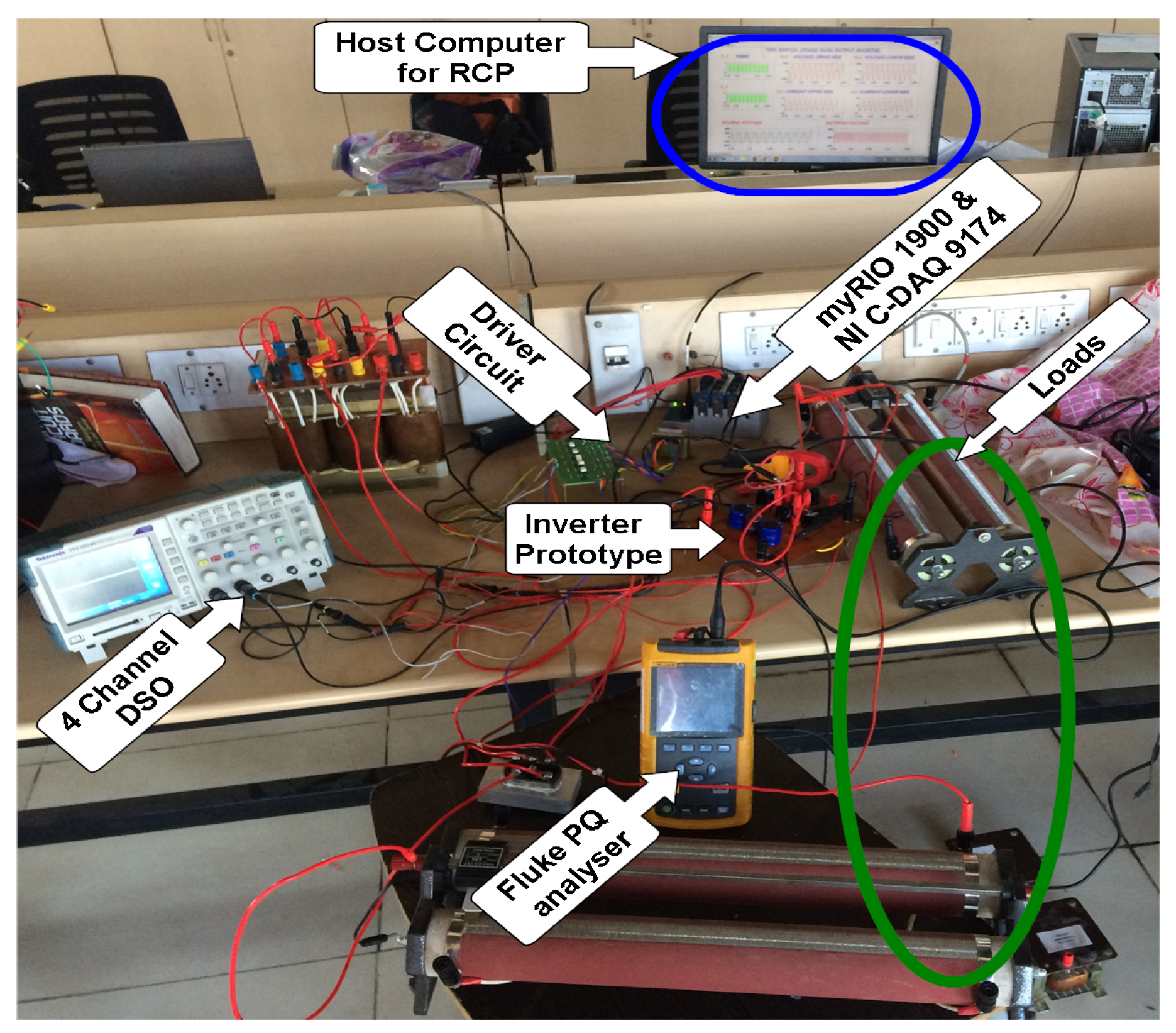
The controller (actuator) is based on NI-1900 MyRIO (Reconfigurable Input/Output) which has Xilinx Zynq-7010 with a combination of Artix-7 FPGA processor, dual-core ARM Cortex-A9 real-time processor and, onboard WIFI. As an advantage of RIO architecture and WIFI, the physical equipment at a remote location is easily controlled. The terminals are reconfigurable as per the requirements. This leads this test bench to be utilized for all power electronics prototype testing. The control algorithm is programmed in NI-My RIO 1900 and connected to the physical device gate driver TI SM72295. The experimental setup is shown in Figure 5.
5. Cyber Layer—LabVIEW Based CPS
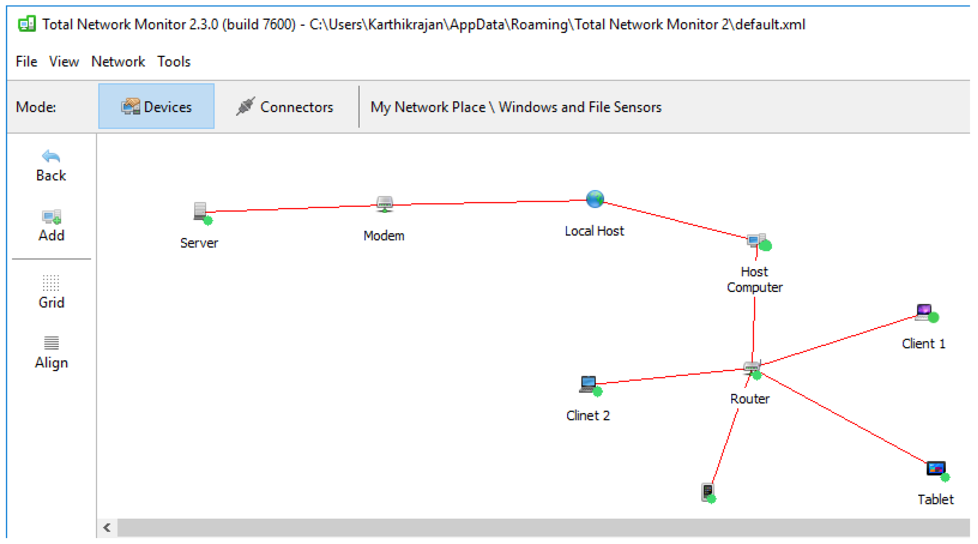
The combination of the physical layer and the cyber–physical layer is integrated into the cyber layer. The cyber layer has a host computer with server and monitoring station (control center). The data transmission and security is the major concern in the cyber layer. The traditional data transmission is not sufficient to transfer large data in CPS. In order to satisfy the needs, the CPS must have the inbuilt transmission systems. The MyRIO has inbuilt Wi-Fi for data exchange between the host and target. While considering the security of the connection, It utilizes the TCP protocol with SSL.x.509 secured layer to enhance the security. The host computer with LabVIEW has the web service management tool for creating the secured URL. The URL mapping is given by https://localhost:portaddress/webservice.html. The LabVIEW has the inbuilt server for the data exchange with a secured network. The collected data from the target is monitored and controlled through the web browser. This method has good live data support, good interaction between the client and user. The network monitoring and active devices monitoring across the network is tracked using the total network monitor. Figure 6 depicts the network map of the system.
6. Results and Discussions
The performance of the proposed dual output inverter with ISMC control strategy is tested and monitored through the CPS system. The analysis was performed under various test conditions like equal output voltage at both the upper and lower side, the different output voltage in upper and lower side and inverter analyzed with and without load variations. The control strategy is implemented using a reconfigurable input/output (RIO) processor. The hardware prototype is fabricated to demonstrate the proposed inverter. The prototype specifications are given in Table 3.
6.1. Steady State Performance
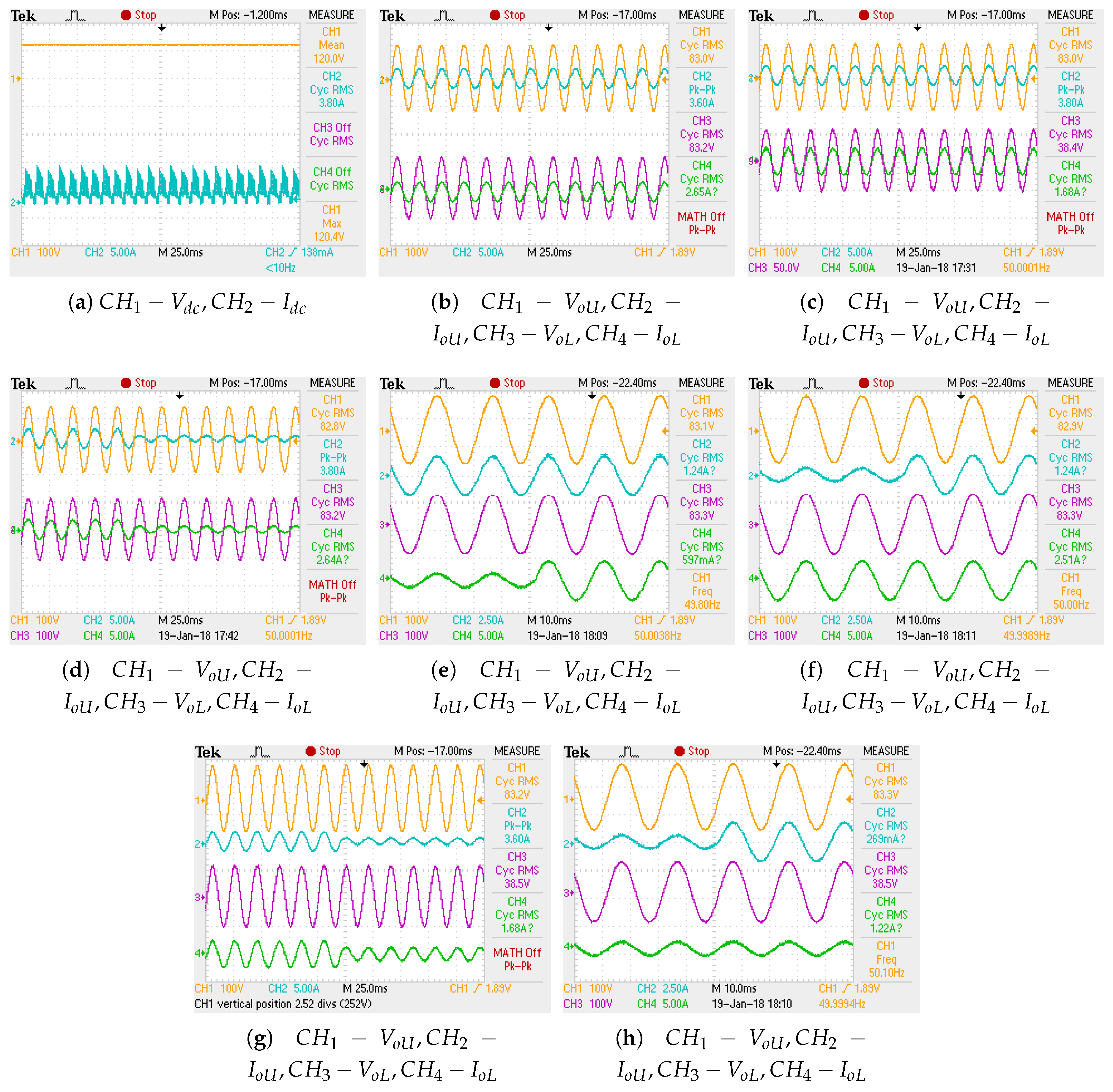
The steady-state performance of the dual output current source inverter is analyzed with an ISMC-based control strategy. The tracking performance of ISMC is discussed in Section 4.2 and performance the comparison of SMC with ISMC is plotted in Figure 4a,b. The IMSC alleviates the steady-state error and settles at 0.05 s. Figure 7 shows the performance of dual output inverter with ISMC.
The DC voltage () and current () are shown in Figure 7a. Due to the current source inverter configuration, the DC link inductor limits the sudden changes in the current and the distortion will get reduced. Figure 7b depicts the dual output voltage and current for 50 Hz operation at EV mode. The dual output current source inverter delivers 83 V at both loads ends (, ) due to the DC link of 120 V. The upper load current () 3.60 A is observed and lower output current () is 2.65 A. The dual output CSI can deliver different voltages (DV mode). In this mode, the upper output voltage is similar to full bridge inverter and lower output voltage similar to a half bridge inverter.
Figure 7c shows the upper output voltage () as 83 V and lower voltage () as 38.4 V. The upper load current () observed is 3.80 A and lower load current () observed is 1.68 A. The inverter is operated at both EV and DV mode with ISMC.
6.2. Response to Load Variations
Figure 7d depicts the step change in both upper and lower load of the dual output current source inverter when it operates in EV mode. The inverter operates at 50 Hz, the output voltage of upper () and lower voltage () is 83 V. The IMSC has a robust response to the load variation and maintains the voltage at the desired level. Figure 7e,f represent the dual output current source inverter waveforms when a sudden step change in upper or lower load. Figure 7e shows the upper () and lower voltage () respectively. The change in upper load () and current observed is 1.24 A and lower load current () results in 597 mA and waveforms shows the change in load. From Figure 7f the EV mode operation with a step change in upper load is observed with 83 V in upper and lower. The load current is 1.24 A and 2.51 A respectively.
In Figure 7g, the performance of the inverter with ISMC is shown. The resultant waveform sohws the operation of the inverter at a different voltage (DV mode) with variations in load current. Figure 7g shows the upper voltage () 83 V and lower voltage () 38 V with variations in upper load current () and lower load current ().
In Figure 7h, the performance of inverter in DV mode with a step change in upper load is analyzed and corresponding upper load current () is 269 mA. The lower load current () inferred is 1.22 A. The overall observations from Figure 7 shows that dual output current source inverter has the capability of supplying two independent loads of same (EV mode) and different voltage (DV mode). The dual output current source inverter has the capability of supplying two independent loads of equal (EV mode) and different voltage (DV mode). The dual output inverter can be used in renewable applications to simultaneously feed power to the grid and to the stand-alone load. In electric drive applications to operate two different machines of the same or different voltage level. The selection of DC link inductor should be concentrated more to obtain the maximum performance of the inverter. Gate pulse generation of the middle switches is critical due to dual operation.
6.3. Harmonic Analysis
The performance of the inverter is analyzed with a single-phase power quality analyzer (Fluke analyzer). The harmonic analysis is performed at EV and DV mode. The THD is tabulated in Table 4.
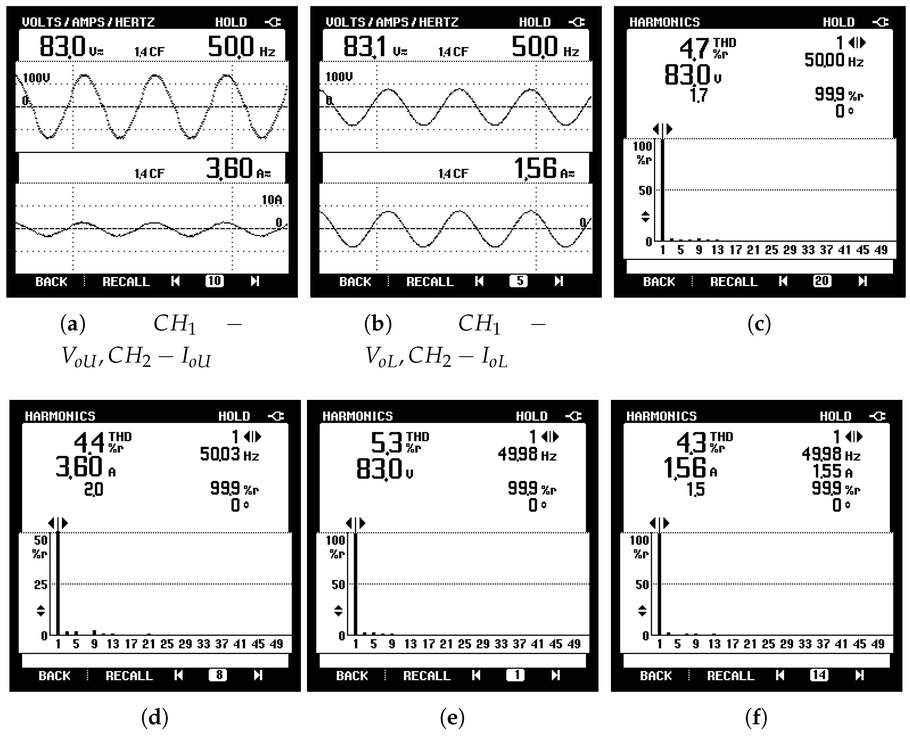
Figure 8 depicts the output voltage and current of the Inverter in EV mode. From Figure 8a, the upper voltage () and upper current () are observed. Figure 8b shows the lower voltage () and lower current (). The total harmonic distortion (THD) of upper load voltage and current is observed from Figure 8. Figure 8c depicts the THD of upper voltage () is 4.7% and from Figure 8d it is observed that THD of upper current () is 4.4%. The total harmonic distortion (THD) of lower load voltage and current is observed from Figure 8. From Figure 8e the THD of lower voltage () observed is 5.3%. Figure 8f depicts the THD of lower current () is 4.3%. The THD observed from the results depicts that the THD is under the acceptable limit as per standards IEEE519-2014.
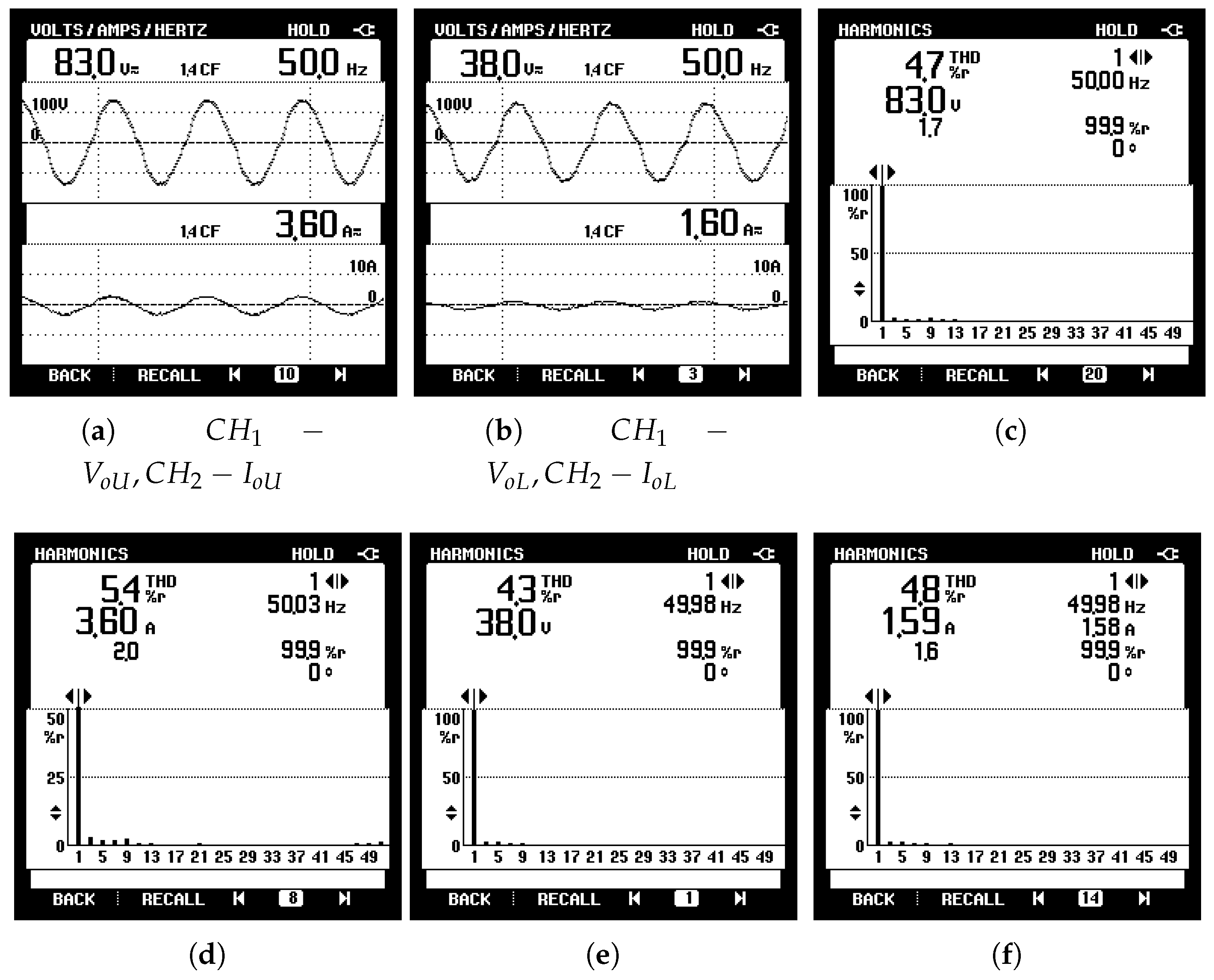
Figure 9 depicts the output voltage and current of the Inverter in DV mode. From Figure 9a the upper voltage () and upper current () is observed. Figure 9b shows the lower voltage () and lower current (). The total harmonic distortion (THD) of upper load voltage and current is observed from Figure 9. Figure 9c depicts the THD of upper voltage () is 4.7% and from Figure 9d it is observed that THD of upper current () is 5.4%. The total harmonic distortion (THD) of lower load voltage and current is observed from Figure 9. From Figure 9e the THD of lower voltage () observed is 4.3%. Figure 9f depicts the THD of lower current () is 4.8%. The THD observed from the results depicts that the THD is under the acceptable limit as per standards IEEE519-2014.
6.4. Voltage Stress
The inverter model has six-switches to . The voltage stress of the switches calculated by the peak voltage across the collector and emitter terminals. The voltage stress is given by,
6.5. Loss Analysis
The total power loss of the IGBT is given by,
where, is the conduction loss of IGBT at high side, is the conduction loss of IGBT at low side, is the switching loss of IGBT.
6.5.1. IGBT Conduction Loss
The conduction loss occurs when the IGBT or free wheeling diode is in ON state. The conduction loss on high side of the inverter is given by,
The conduction loss on low side is given by,
where, the and is the resistance of IGBT for high and low side respectively.
6.5.2. IGBT Switching Loss
The power loss occurred during the transition and based on switching frequency. The switching loss is calculated by,
where, and is the high time and fall time of IGBT. is the switching frequency.
The total loss compared to a conventional current source inverter (CSI) is tabulated in Table 5. The total loss calculated for two conventional inverters to deliver dual loads is 22.064 W and proposed dual output CSI has 16.548 W. The proposed dual output CSI has the ability to supply two aindependent loads with the reduced number of semiconductor switches.
6.6. Online Monitoring
The CPS design is implemented to evaluate the performance of CSI dual output inverter. The control and monitoring of the target device are done through the internet browser. The connection is based on TCP protocol and SSL.x.509 secured layer is used to ensure the webpage security.
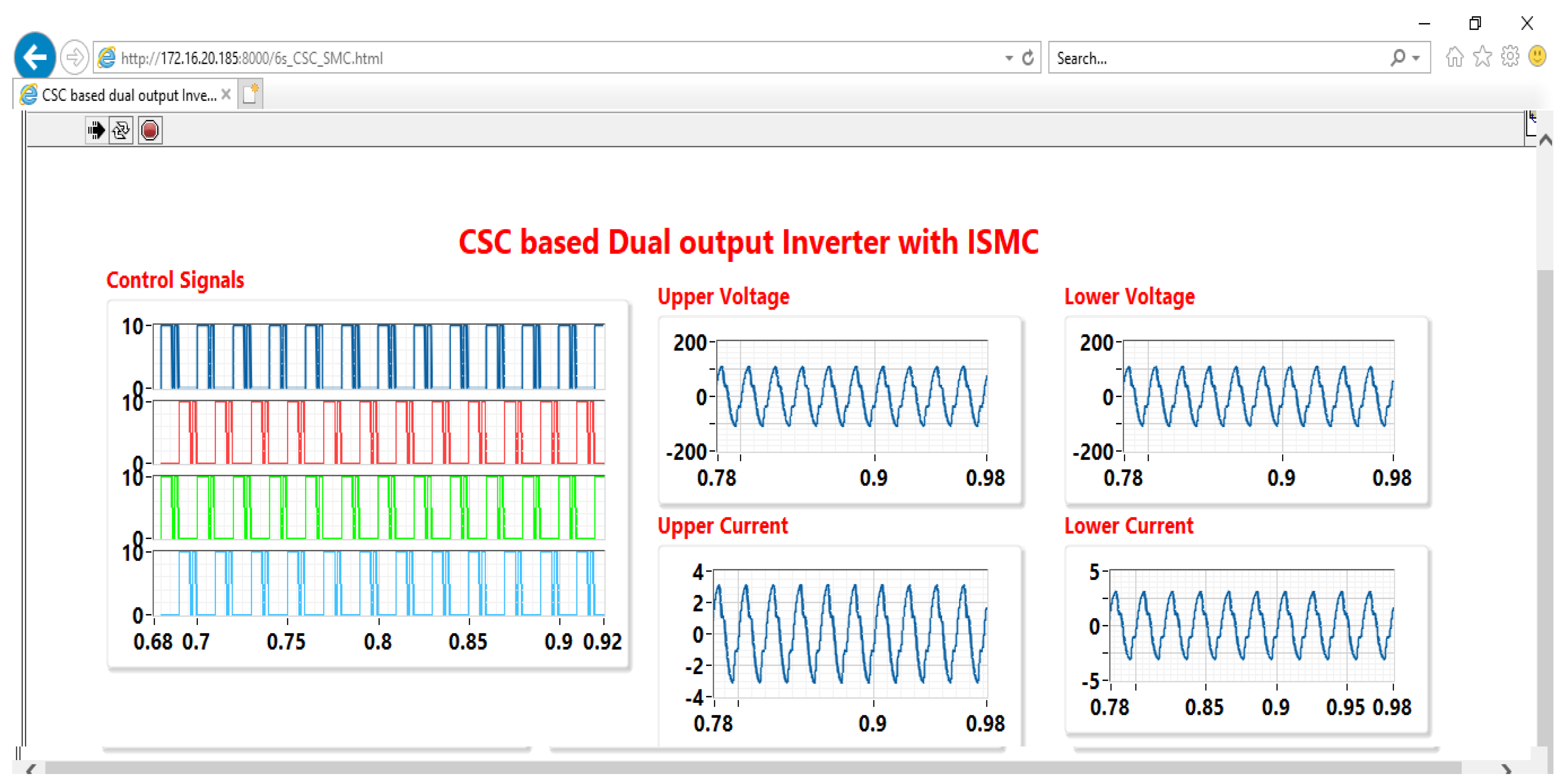
From Figure 10 the online monitoring of dual output CSC inverter performance is displayed. The resilient cyber infrastructure designed using single domain has the advantage of lower transport delay and easy implementation compared to other methods. The network monitoring of server and client is monitored by Total Network Monitor as shown in Figure 6. The incorporation of CPS in the inverter model leads to the development of smart grids, smart manufacturing in industries for controlling inverters in drives and smart learning with decentralized control of multiple systems.
7. Conclusions
The dual output current source inverter topology operating in two different voltage modes is presented. A significant advantage of this topology is that it can supply power simultaneously to two different loads of equal (EV mode) and/or different (DV mode) voltages for microgrid applications. The control strategy based on sliding mode controllers is analyzed. The conventional sliding function has the steady-state error of 10% for voltage control and 5% for current control. To alleviate the steady-state error, an additional integral term is introduced and integral sliding mode control is derived for the dual output current source inverter. The cyber twin approach for the control of power electronics circuits is introduced and notable results are achieved. Reconfigurable Input/Output processors (MyRIO-1900) with cyber physical test bench is developed to implement continuous time-based control strategies, processors with high speed data processing is required. The development the cyber physical system for an inverter leads to the development of virtual laboratories and smart grids.
Author Contributions
Conceptualization, K.S. and I.A.; Methodology, K.S. and I.A.; Supervision, I.A.
Funding
This research received no external funding.
Acknowledgments
The authors like to thanks the smart grid laboratory, power electronics laboratory and advanced drives laboratory, School of Electrical Engineering, Vellore Institute of Technology(VIT), Chennai for carrying out this project.
Conflicts of Interest
The authors declare that they have no conflict of interest.
References
- Pichan, M.; Karimi, M.; Simorgh, H. Improved low-cost sliding mode control of 4-leg inverter for isolated microgrid applications. Int. Trans. Electr. Energy Syst. 2018. [Google Scholar] [CrossRef]
- Li, T.; Cheng, Q. Structure analysis and sliding mode control of new dual quasi-Z-source inverter in microgrid. Int. Trans. Electr. Energy Syst. 2018. [Google Scholar] [CrossRef]
- Jacobina, C.; de Freitas, I.; Lima, A. DC-Link Three-Phase-to-Three-Phase Four-Leg Converters. IEEE Trans. Ind. Electron. 2007, 54, 1953–1961. [Google Scholar] [CrossRef]
- Yu, X.; Starke, M.; Tolbert, L.; Ozpineci, B. Fuel cell power conditioning for electric power applications: A summary. IET Electr. Power Appl. 2007, 1, 643. [Google Scholar] [CrossRef]
- Fatemi, A.; Azizi, M.; Mohamadian, M.; Varjani, A.Y.; Shahparasti, M. Single-Phase Dual-Output Inverters With Three-Switch Legs. IEEE Trans. Ind. Electron. 2013, 60, 1769–1779. [Google Scholar] [CrossRef]
- Nguyen, B.L.H.; Cha, H.; Kim, H.G. Single-Phase Six-Switch Dual-Output Inverter Using Dual-Buck Structure. IEEE Trans. Power Electron. 2017. [Google Scholar] [CrossRef]
- Senthilnathan, K.; Annapoorani, I. Implementation of unified power quality conditioner (UPQC) based on current source converters for distribution grid and performance monitoring through LabVIEW Simulation Interface Toolkit server: A cyber physical model. IET Gener. Transm. Distrib. 2016, 10, 2622–2630. [Google Scholar] [CrossRef]
- Komurcugil, H. Integral sliding-mode-based current-control strategy for single-phase current-source inverters. Electr. Eng. 2011, 93, 127–136. [Google Scholar] [CrossRef]
- Li, R.T.H.; Chung, H.S.; Chan, T.K.M. An Active Modulation Technique for Single-Phase Grid-Connected CSI. IEEE Trans. Power Electron. 2007, 22, 1373–1382. [Google Scholar] [CrossRef]
- Komurcugil, H. Steady-State Analysis and Passivity-Based Control of Single-Phase PWM Current-Source Inverters. IEEE Trans. Ind. Electron. 2010, 57, 1026–1030. [Google Scholar] [CrossRef]
- Kukrer, O.; Komurcugil, H.; Doganalp, A. A Three-Level Hysteresis Function Approach to the Sliding-Mode Control of Single-Phase UPS Inverters. IEEE Trans. Ind. Electron. 2009, 56, 3477–3486. [Google Scholar] [CrossRef]
- Afghoul, H.; Krim, F.; Babes, B.; Beddar, A.; Kihel, A. Design and real time implementation of sliding mode supervised fractional controller for wind energy conversion system under sever working conditions. Energy Convers. Manag. 2018, 167, 91–101. [Google Scholar] [CrossRef]
- Komurcugil, H.; Biricik, S. Time-Varying and Constant Switching Frequency-Based Sliding-Mode Control Methods for Transformerless DVR Employing Half-Bridge VSI. IEEE Trans. Ind. Electron. 2017, 64, 2570–2579. [Google Scholar] [CrossRef]
- Morales, J.; de Vicuna, L.G.; Guzman, R.; Castilla, M.; Miret, J. Modeling and Sliding Mode Control for Three-Phase Active Power Filters Using the Vector Operation Technique. IEEE Trans. Ind. Electron. 2018, 65, 6828–6838. [Google Scholar] [CrossRef]
- Ahmadzadeh, S.; Markadeh, G.A.; Blaabjerg, F. Voltage regulation of the Y-source boost DC–DC converter considering effects of leakage inductances based on cascaded sliding-mode control. IET Power Electron. 2017, 10, 1333–1343. [Google Scholar] [CrossRef]
- Musa, A.; Sabug, L.R.; Monti, A. Robust Predictive Sliding Mode Control for Multiterminal HVDC Grids. IEEE Trans. Power Deliv. 2018, 33, 1545–1555. [Google Scholar] [CrossRef]
- Wang, H.; Ge, X.; Liu, Y.C. Second-Order Sliding-Mode MRAS Observer Based Sensorless Vector Control of Linear Induction Motor Drives for Medium-Low Speed Maglev Applications. IEEE Trans. Ind. Electron. 2018. [Google Scholar] [CrossRef]
- Dai, Y.; Zhuang, S.; Ren, H.; Chen, Y.; He, K. Discrete modelling and state-mutation analysis for sliding mode controlled non-isolated grid-connected inverter with H6-type. IET Power Electron. 2017, 10, 1307–1314. [Google Scholar] [CrossRef]
- Yang, Q.; Saeedifard, M.; Perez, M.A. Sliding Mode Control of the Modular Multilevel Converter. IEEE Trans. Ind. Electron. 2018. [Google Scholar] [CrossRef]
- Sankar, K.; Jana, A.K. Nonlinear multivariable sliding mode control of a reversible PEM fuel cell integrated system. Energy Convers. Manag. 2018, 171, 541–565. [Google Scholar] [CrossRef]
- Instruments, N. NI Single-Board RIO General-Purpose Inverter Controller Features; Technical Report; National Instruments: Austin, TX, USA, 2012. [Google Scholar]
- Balda, J.C.; Mantooth, A.; Blum, R.; Tenti, P. Cybersecurity and Power Electronics: Addressing the Security Vulnerabilities of the Internet of Things. IEEE Power Electron. Mag. 2017, 4, 37–43. [Google Scholar] [CrossRef]
- Van der Meer, A.A.; Palensky, P.; Heussen, K.; Bondy, D.M.; Gehrke, O.; Steinbrinki, C.; Blanki, M.; Lehnhoff, S.; Widl, E.; Moyo, C.; et al. cyber–physical energy systems modeling, test specification, and co-simulation based testing. In Proceedings of the 2017 Workshop on Modeling and Simulation of Cyber–Physical Energy Systems (MSCPES), Pittsburgh, PA, USA, 18–21 April 2017. [Google Scholar]
- Yoo, H.; Shon, T. Challenges and research directions for heterogeneous cyber–physical system based on IEC 61850: Vulnerabilities, security requirements, and security architecture. Future Gener. Comput. Syst. 2016, 61, 128–136. [Google Scholar] [CrossRef]
- Maffei, A.; Srinivasan, S. A cyber–physical Systems Approach for Implementing the Receding Horizon Optimal Power Flow in Smart Grids. IEEE Trans. Sustain. Comput. 2017. [Google Scholar] [CrossRef]
- Ntalampiras, S.; Soupionis, Y. Gaussian Mixture Modeling for Detecting Integrity Attacks in Smart Grids. Electronics 2016, 5, 82. [Google Scholar] [CrossRef]
- Sun, C.C.; Liu, C.C.; Xie, J. cyber–physical System Security of a Power Grid: State-of-the-Art. Electronics 2016, 5, 40. [Google Scholar] [CrossRef]
- Lee, E.A. Computing Foundations and Practice for CPS: A Preliminary Report; Technical Report; University of California: Berkeley, CA, USA, 2007. [Google Scholar]
- Liu, Y.; Peng, Y.; Wang, B.; Yao, S.; Liu, Z. Review on cyber–physical systems. IEEE/CAA J. Autom. Sin. 2017, 4, 27–40. [Google Scholar] [CrossRef]
- Andalam, S.; Ng, D.J.X.; Easwaran, A.; Thangamariappan, K. Contract-based Methodology for Developing Resilient Cyber-Infrastructure in the Industry 4.0 Era. IEEE Embed. Syst. Lett. 2018. [Google Scholar] [CrossRef]
- Nguyen, V.; Besanger, Y.; Tran, Q.; Nguyen, T. On Conceptual Structuration and Coupling Methods of Co-Simulation Frameworks in cyber–physical Energy System Validation. Energies 2017, 10, 1977. [Google Scholar] [CrossRef]
- Gonzalez, I.; Calderon, A.; Andujar, J. Novel remote monitoring platform for RES-hydrogen based smart microgrid. Energy Convers. Manag. 2017, 148, 489–505. [Google Scholar] [CrossRef]
- Zhang, F.; Liu, M.; Zhou, Z.; Shen, W. An IoT-Based Online Monitoring System for Continuous Steel Casting. IEEE Internet Things J. 2016, 3, 1355–1363. [Google Scholar] [CrossRef]
- Moness, M.; Moustafa, A.M. A Survey of cyber–physical Advances and Challenges of Wind Energy Conversion Systems: Prospects for Internet of Energy. IEEE Internet Things J. 2016, 3, 134–145. [Google Scholar] [CrossRef]
- Gonizzi, P.; Ferrari, G.; Gay, V.; Leguay, J. Data dissemination scheme for distributed storage for IoT observation systems at large scale. Inf. Fusion 2015, 22, 16–25. [Google Scholar] [CrossRef]
- Zhou, P.; Huang, G.; Zhang, L.; Tsang, K.F. Wireless sensor network based monitoring system for a large-scale indoor space: Data process and supply air allocation optimization. Energy Build. 2015, 103, 365–374. [Google Scholar] [CrossRef]
- Aslan, Y.E.; Korpeoglu, I.; Ulusoy, O. A framework for use of wireless sensor networks in forest fire detection and monitoring. Comput. Environ. Urban Syst. 2012, 36, 614–625. [Google Scholar] [CrossRef] [Green Version]
- Haag, S.; Anderl, R. Digital twin—Proof of concept. Manuf. Lett. 2018, 15, 64–66. [Google Scholar] [CrossRef]
- Alam, K.M.; Saddik, A.E. C2PS: A Digital Twin Architecture Reference Model for the Cloud-Based cyber–physical Systems. IEEE Access 2017, 5, 2050–2062. [Google Scholar] [CrossRef]
- Zhang, H.; Liu, Q.; Chen, X.; Zhang, D.; Leng, J. A Digital Twin-Based Approach for Designing and Multi-Objective Optimization of Hollow Glass Production Line. IEEE Access 2017, 5, 26901–26911. [Google Scholar] [CrossRef]
- Qi, Q.; Tao, F. Digital Twin and Big Data Towards Smart Manufacturing and Industry 4.0: 360 Degree Comparison. IEEE Access 2018, 6, 3585–3593. [Google Scholar] [CrossRef]
Figure 1.
Block diagram of cyber twin.

Figure 2.
System Configuration.

Figure 3.
Schematic of Mircogrid.

Figure 4.
Performance comparision of SMC and ISMC: (a) Input current, (b) Output Voltage.

Figure 5.
Experimental Setup.

Figure 6.
Network Monitor.

Figure 7.
Prototype Results: (a) DC voltage and current, (b) EV mode output voltage and load current, (c) DV mode output voltage and load current, (d) EV mode output voltage and load current with step change, (e) EV mode output voltage and load current with step change in lower load, (f) EV mode output voltage and load current with step changes in upper load, (g) DV mode output voltage and load current with step changes in load, (h) DV mode output voltage and load current with step change in upper load.

Figure 8.
Prototype Results: (a) Upper output voltage and load current, (b) Lower output voltage and load current, (c) Upper output voltage THD, (d) Lower output voltage THD, (e) Upper Current THD, (f) Lower Current THD.
Figure 8.
Prototype Results: (a) Upper output voltage and load current, (b) Lower output voltage and load current, (c) Upper output voltage THD, (d) Lower output voltage THD, (e) Upper Current THD, (f) Lower Current THD.

Figure 9.
Prototype Results: (a) Upper output voltage and load current, (b) Lower output voltage and load current, (c) Upper output voltage THD, (d) Lower output voltage THD, (e) Upper Current THD, (f) Lower Current THD.
Figure 9.
Prototype Results: (a) Upper output voltage and load current, (b) Lower output voltage and load current, (c) Upper output voltage THD, (d) Lower output voltage THD, (e) Upper Current THD, (f) Lower Current THD.

Figure 10.
Monitoring Screen.


Table 1.
CPS comparison.
| Ref. | Sensors Type | Mode | Network/ Monitoring | Programming Platform |
|---|---|---|---|---|
| [33] | RFID Tag | Zigbee, CAN, RFID | XML | Multi domain |
| [34] | RTU | WSN | CC studio, SCADA/HMI | Multi domain |
| [35] | SenseLab Sensor | WSN | Cooja network simulator | Multi domain |
| [36] | Sensor nodes Green orbs | WSN, Zigbee | Green orbs host computer | Multi domain |
| [32] | Sensors PLC | WIFI | LabVIEW JIL server | Multi domain |
| Proposed | NI Sensors MyRIO | WIFI | LabVIEW VI Server | Single domain |
Table 2.
Comparison of Inverters.
| Inverter Type | Switches | Source Type | EV | DV |
|---|---|---|---|---|
| Dual phase with single DC bus with split Capacitor | 4 | Voltage | Yes | No |
| Dual phase with three wire | 6 | Voltage | Yes | No |
| Dual phase dual DC bus | 4 | Voltage | Yes | No |
| Dual phase with transformer | 4 | Voltage | Yes | No |
| Dual output VSI | 6 | Voltage | Yes | No |
| Single port conventional CSI | 4 | Current | Yes | No |
| Proposed | 6 | Current | Yes | Yes |
Table 3.
System Parameters.
| Parameters | Values (Units) |
|---|---|
| Maximum Rated Power | 1 kW |
| DC Voltage | 120 V |
| Inductor | 10 mH |
| IGBT | IRG4BC30S |
| Controller | NI myRIO 1900 |
| Data Acquisition Systems | NI C-DAQ 9174 |
| Driver Circuit | Texas Instruments SM72295 |
| Server | NI web server |
| Network Monitoring | Total Network Manager (TNM) |
| Oscilloscope | Textronix TPS 2024B four channel |
Table 4.
THD.
| THD | Upper Side THD % | Lower Side THD % | ||
|---|---|---|---|---|
| EV | DV | EV | DV | |
| Voltage THD | 4.7 | 4.7 | 5.3 | 4.3 |
| Current THD | 4.4 | 5.4 | 4.3 | 4.8 |
Table 5.
Loss comparison.
| Inverter Type | No of Outputs | No of Switches | Total Loss (w) |
|---|---|---|---|
| Conventional CSI | 1 | 4 | 11.032 |
| Two conventional CSI | 2 | 8 | 22.064 |
| Proposed dual output CSI | 2 | 6 | 16.548 |
© 2018 by the authors. Licensee MDPI, Basel, Switzerland. This article is an open access article distributed under the terms and conditions of the Creative Commons Attribution (CC BY) license (http://creativecommons.org/licenses/by/4.0/).
Share and Cite
MDPI and ACS Style
Senthilnathan, K.; Annapoorani, I. Multi-Port Current Source Inverter for Smart Microgrid Applications: A Cyber Physical Paradigm. Electronics 2019, 8, 1. https://doi.org/10.3390/electronics8010001
AMA Style
Senthilnathan K, Annapoorani I. Multi-Port Current Source Inverter for Smart Microgrid Applications: A Cyber Physical Paradigm. Electronics. 2019; 8(1):1. https://doi.org/10.3390/electronics8010001
Chicago/Turabian StyleSenthilnathan, Karthikrajan, and Iyswarya Annapoorani. 2019. "Multi-Port Current Source Inverter for Smart Microgrid Applications: A Cyber Physical Paradigm" Electronics 8, no. 1: 1. https://doi.org/10.3390/electronics8010001
Note that from the first issue of 2016, this journal uses article numbers instead of page numbers. See further details here.