Maximal Q Factor for an On-Chip, Fuse-Based Trimmable Capacitor


1
Department of Computer Science, Electrical and Space Engineering, Luleå University of Technology, 971 87 Luleå, Sweden
2
Department of Physics, Imperial College, London SW7 2AZ, UK
*
Author to whom correspondence should be addressed.
Electronics 2019, 8(1), 62; https://doi.org/10.3390/electronics8010062
Submission received: 3 October 2018
/
Revised: 12 December 2018
/
Accepted: 4 January 2019
/
Published: 5 January 2019
(This article belongs to the Special Issue All-Digital Time-Mode Approaches for Mixed Analog-Digital Signal Processing)
Abstract
:This paper presents a circuit for realising a fuse-programmable capacitor on-chip. The trimming mechanism is implemented using integrated circuit fuses which can be blown in order to lower the resulting equivalent capacitance. However, for integrated circuits, the non-zero fuse resistance for active fuses and finite fuse resistance for blown fuses limit the Q factor of the resulting capacitor. In this work, we present a method on how to arrange the fuses in order to achieve maximal worst-case Q factor for the given circuit topology given the process parameters and requirements on capacitance. We also analyse and discuss the accuracy and limitations of the topology with regard to fuse resistance and parasitic elements such as bond pads.
1. Introduction
The goal to design resonant circuits for single-chip RF systems has created the need for trimmable [1] IC capacitors. Applications for such circuits exist in the field of wireless transfer of power directly to a single-chip system, where the RF inductor is integrated on the die. Examples of applications include implantable chips in humans for biomedical purposes [2,3], and sensors for condition monitoring of power semiconductors, where a wireless power supply and communication interface provides galvanic isolation from the high-voltage power semiconductors [4,5].
For both examples, the on-chip coils would be optimised based on the properties of the surrounding materials: tissue data [6] in the case for biomedical implants, and power semiconductor module geometry data [5] in the case for sensors for condition monitoring. In these types of application, a capacitor can be used to form a resonant circuit with the receiver on-chip coil, which boosts the voltage induced in the coil. However, for resonant circuits in single-chip systems such as described above, the obtained resonant frequency may deviate from the desired one because of large tolerances in the IC manufacturing process. Obtaining a specific frequency can be important for RF applications for which the frequency must lie within a frequency band which allows sufficient energy to be radiated, for example an ISM band [7]. Tunability is also important for applications where many devices must be powered by the same transmitter and thus operate at the same frequency. One way to adjust the resonant frequency is to trim the value of the capacitor in an LC circuit.
As an alternative to relatively costly laser-trimmed [8] IC capacitors, in this paper we discuss how to optimise fuse-based binary-weighted trimmable capacitors in order to maximise their Q factors which in turn will maximise the Q factors for any resonant circuits built from such capacitors. One such circuit could be an LC circuit consisting of an RF receiver coil and a resonant trimmable capacitor used for frequency tuning. The main issue we address is the effect of non-zero and finite resistance for active and blown IC fuses, respectively.
Although the theory presented in this work is valid not only for fuses, but also for semiconductor switches such as MOSFETs, this paper addresses only fuses. This decision is motivated by the fact that for applications which require a wireless power supply, no power source is available to bias a semiconductor into a desired switching state. Furthermore, even if semiconductors were to be used, such as in [9], effects from e.g., parasitic capacitance and temperature-dependent leakage current would still have to be taken into account.
Furthermore, because fuses are one-time programmable, if possible, we recommend using capacitive structures which have good temperature and bias stability such as MIM capacitors [10], which also exhibit high Q factors. In contrast, using MOSFET capacitors would introduce a strong dependence on bias for the resulting capacitance [11]. Furthermore, if no power source is available for bias, the MOSFETs would be biased in the region where the capacitance varies the most and the variation in capacitance with voltage would be extremely strong [11], defeating the purpose of trimming.
For biomedical implants, a concern could be that the impedance of an implanted coil would be sensitive to the electromagnetic properties of the surrounding tissue which are only known approximately and may change over time, which in turn would result in a change in resonant frequency. However, the encapsulation of the IC chip can be made comparable in size to the coil diameter, for example a chip with a 1 encapsulation. In such a case, the electromagnetic fields generated by the on-chip coil will extend mainly into the encapsulation material (whose electromagnetic properties are known to a high accuracy and do not change) and not into the surrounding tissue. Thus the resonance frequency can be trimmed before implantation and will not change over time.
The paper is organised as follows. In Section 2, we introduce the circuit and discuss how to optimise it for maximum Q factor and in Section 3 we discuss the accuracy of the optimised circuit. In Section 4, we present an example relating the theory to an application and discuss the results. The conclusion is presented in Section 5.
2. Trimmable Capacitor Bank
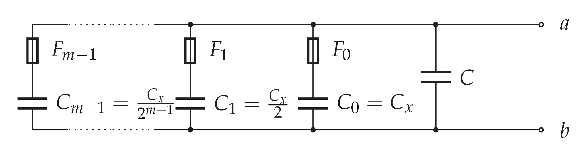
Consider the trimmable capacitor bank shown in Figure 1. The circuit comprises one base capacitor, C, in parallel with m binary-weighed trim capacitors, , distributed as . The trim capacitors can be deactivated by blowing their corresponding fuse in . The equivalent capacitance, , seen between nodes a and b can be written as
where is 0 if fuse n is blown and 1 if it is active. From Equation (1), it can be seen that by letting represent bit n of an m-bit binary number, can be controlled from C to with the resolution of the smallest trim capacitance, . Because is the sum of all the trim capacitances, it can be written as
By solving Equation (2) for , we arrive at the following expression:
Thus, from the base capacitance, C, and trim capacitance, , needed for the application, values can be selected for all the capacitors in the circuit of Figure 1.
2.1. Finite/Non-Zero Fuse Resistance
For ICs, both the fuse on-resistance, , and off-resistance, can be significant. In many process technologies, a unit fuse is available with a fixed on- and off-resistance and for the examples in this work, values of and , relevant to a 180 process, are assumed. It is however possible to realise arbitrary on- and off-resistances, and by connecting a number of fuses in series and/or parallel and then either blowing all or none of the fuses in a branch. Because and are constant, the on-resistance of the resulting network will always be linearly related to its off-resistance by a factor,
The question thus arises on how to select (or, equivalently ) in order to maximise the Q factor for the resulting capacitor for the worst-case configuration of active/blown fuses. It should be noted that both and is highly process dependent, which may make fuse trimming less attractive in some processes than others, particularly those in which is small, which will be demonstrated later in this section.
2.2. Q Factor Optimisation for a Single Branch
Consider starting with the base capacitance, C, and adding a single fuse-controlled branch to that circuit. The resulting Q factor, , for arbitrarily selected component values are plotted in Figure 2 as a function of the fuse scaling factor, , with the fuse resistance, , attaining values for both active and blown fuses. Here is the factor by which a fuse is scaled by a series and/or parallel connection that gives a scaled fuse resistance , and also and . In order to maximise the resulting worst-case Q factor, we want to find the value of for which the worst-case for both cases of is as large as possible. That is, we want to maximise the function
From the figure, it can be seen that the maximum is obtained either for very small values for or for very large values for . In fact, tends towards infinity for such values. The reason for this is that, for very small , the fuse behaves as a short circuit for both its active and blown state and thus does not contribute significantly to the total equivalent resistance of the circuit. The contrary is true for very large , where the fuse behaves as an open circuit for both cases and thus the branch does not contribute significantly to the equivalent impedance. Thus, if we choose such extreme values for , the resulting equivalent capacitance can no longer be controlled by the fuse. Therefore, we must choose a value for in a region where the fuse behaves as a short circuit for active fuses (to the left of the minimum of the blue solid line), and as an open circuit for blown fuses (to the right of the minimum for the red dashed line). It can be seen from Figure 2 that a local maximum for within this region occurs at the intersection point of the of the curves representing the Q factor for and , respectively.
Note that this point represents the fuse resistances for which the Q factor has degraded equally for the active and blown states of the fuse. Deviating from this point increases the Q factor for one of these states, but decreases it for the other. The intersection point thus represents the highest possible worst-case Q factor for the equivalent capacitor. It should also be noted that Figure 2 assumes infinite Q factors for all involved capacitors. If IC capacitors can be manufactured with a Q factor of , for extreme values for , would approach asymptotically instead of tending towards infinity. In fact, this behaviour is shown in a lighter shade in the figure. The simplification is made because it is reasonable to assume that the series resistance contributed to one of the capacitors by a scaled fuse will be much larger than the ESR of the capacitor itself. Thus, for non-extreme values for , which are the values we are interested in, will be much larger than .
In the pursuit to find an expression for the intersection point of Figure 2, consider the equivalent impedance, , resulting from the parallel connection of two impedances, and . Here, symbols R and X denote the resistance and reactance, respectively, of the impedance Z with corresponding index. It can be shown that is given by
Regarding the resulting impedance as a capacitor with a series resistance, the resulting Q factor is given by
To find the intersection point of Figure 2 in terms of the scaled fuse resistance, , we set
where is given by Equation (4) and is the scaling factor which can be obtained by a series and/or parallel connection of fuses. Substituting Equation (7) into Equation (8) yields
Solving Equation (9) for yields
Relating this expression to Figure 1, we substitute , and , where is the added capacitance in the branch currently being added, C is the base capacitance including all thus far added branches, R is the resistance in series with C resulting from all fuse resistances from all thus far added branches and is the angular frequency under which the circuit is intended to operate. Thus, as a function of branch number, n, can be written as
Let Q represent the Q factor given by the series combination of C and R. Then, . Substituting this expression into Equation (11) yields
Thus we have arrived at an expression for how to select the scaled fuse resistance, , when adding one fuse-controlled branch to the base capacitance.
2.3. Q Factor Optimisation for Multiple Branches
In order to find for the fuses in each branch, one possible solution is to use Equation (14) recursively for all the branches. However, there is a challenge associated with this approach. Consider adding the first branch to the base capacitance. In this case, it is obvious which value to use for C. However, for the next branch, C might take on two different values depending on whether the fuse will be active or blown in the first branch, so we would also need to consider the case for when C is substituted for . When adding the third branch, there will be four possible values for C. In fact, the number of values would double for each new branch added.
Because of this complexity, we do not pursue this approach further. Instead, we use Equation (14) to obtain an expression for the Q factor, , of the branch being added when its fuse is active:
If only one branch would be added, we could use Equation (15) to know which Q factor it should have in its active state, which would in turn yield a value for . However, as explained above, we don’t know which value to use for C in the coming branches because the fuse configuration is unknown. Thus, it appears that we can only use Equation (15) to find for one of the branches.
However, consider the case when all branches have the same Q factor with all fuses active. We denote this Q factor . The equivalent Q factor does not change if multiple branches with identical Q factor are connected in parallel. Therefore, for a certain fuse configuration, we would have one equivalent Q factor, , for all active branches and one equivalent Q factor, , for all blown branches. Because the Q factor is inversely proportional to the branch resistance, . If we attempt to increase by increasing the Q factor for a single branch, the Q factor for that branch in its blown state will also increase. While this would result in an increased for when this branch is active, it would decrease it for when it is blown. Refer to Figure 2 and note that at the intersection point, an increased would mean a decreased and thus a decreased scaled fuse resistance, . Following the blue solid line from the intersection point for decreasing yields a higher . However, for , following the red dashed line for decreasing yields a lower .
Similarly, we could try to increase the worst-case by increasing . However, this would also increase it for and, by the same reasoning as before, would result in a lower worst-case . Attempting to change the fuse resistance for multiple branches simultaneously will also not improve the worst-case because for the worst-case, the fuse state resulting in the lowest will be in use for each branch. Thus, we conclude that will be maximised when all branches have the same Q factor. This Q factor can be found by considering the equivalent circuit for all branches with the fuses in their active state and then using Equation (15) and substituting for the equivalent parallel resistance for the branches, , to find the Q factor for a branch, , for all n:
This is an expression for the scaled fuse resistance, , for each branch, which yields the maximal worst-case equivalent Q factor, . Here, was used in order to obtain an expression for as a function of . It should be noted that if the exact value for required by Equation (17) cannot be obtained because a prohibitively large number of fuses would be required, an error will be introduced in . Because the Q factor of a capacitor is given by its reactance divided by its resistance (that is, in the case for , divided by ), the relative error in the worst-case will be no greater than the relative worst-case error in , or equivalently, no greater than the relative error in the fuse scaling factor, , in the fuse with the largest relative scaling mismatch.
To obtain an expression for the resulting worst-case equivalent Q factor when a fuse-controlled branch is connected in parallel with the base capacitance, C, we use Equation (7) and substitute
where is the scaled fuse on-resistance obtained for a branch with as series capacitance. The resulting expression is given by
From Equation (23) it can be seen that increasing the ratio of base capacitance to trim capacitance, , increases . This is intuitive because that increases the ratio of capacitance contributed by capacitors with no series resistance to capacitance contributed by capacitors with series resistance. It can also be seen that a higher ratio, , between off and on resistance for the fuses used will increase , which is also intutive because higher quality fuses should yield better Q factors.
It is interesting to note that highest possible worst-case Q factor, , depends only on the ratio between desired base and trim capacitance as well as on the ratio of resistance between blown and active fuses for the process technology and is thus frequency-independent.
3. Capacitance Accuracy
Because is the result of connecting a capacitor with no series resistance in parallel to a number of capacitors with series resistance, the resulting capacitance value will not be exactly equal to the target capacitance. Another contribution to the mismatch in capacitance comes from parasitic elements such as bond pads used to program (blow) the fuses. In this section, we quantify these mismatches.
3.1. Effects of Fuse Resistance
Consider adding a single branch to the base capacitance, C. If the fuse for that branch is active, the contributed capacitance will be slightly lower than the actual value of the capacitor in that branch, , because of the series resistance of the branch. On the other hand, if the fuse for that branch is blown, the intent is that no capacitance should be contributed, but because of the finite fuse resistance, indeed some capacitance will be contributed. Thus, we see that active branches contribute too little capacitance, whereas blown branches contribute too much capacitance. The magnitude of the mismatch of target capacitance to actual capacitance will thus be largest either for all fuses active or for all fuses blown.
For the case for all fuses active, the equivalent impedance, , can be found from Equation (6). Since we are only interested in the difference in capacitance, we are only interested in the reactive part of . Using the substitutions in Equations (18)–(21), it can be shown that the reactive part of is given by
The maximum difference between the target capacitance, , and the capacitance contributed by is given by
Thus, we have arrived at an expression for the maximum error in capacitance, , for all fuses active. It is interesting to note that Equation (27) can be interpreted as follows: The maximum error in capacitance equals the equivalent capacitance of two series-connected capacitors of capacitance C and , respectively, scaled by the factor .
An expression for for the equivalent reactance for the case for all fuses blown, here denoted , can be obtained from Equation (6) using the substitutions in Equations (19)–(21), and substituting
Utilising Equation (16) and solving for , is given as
The maximum difference between the target capacitance, C, and the capacitance contributed by is given by
It can be shown that substituting Equation (29) into Equation (30) yields
which is exactly equal in magnitude to in Equation (26), but with opposite sign; . The error in capacitance for any fuse configuration, , will thus lie within the interval
In assessing the accuracy we have neglected the effects of capacitance variations with respect to process, voltage and temperature. As stated in the introduction, we recommend using MIM capacitors to realise the trim capacitor presented in this work because of their temperature and voltage stability [10]. However, the capacitors will still be subject some variation, especially as a result of variations in the manufacturing process. Because fuses are one-time programmable, they can not be used to compensate for variations in temperature or voltage which change over time, but they can be used to compensate for process variation. As an example, consider the application of an LC resonator discussed in the introduction. If the low-frequency inductance and the untrimmed resonant frequency are measured, the base capacitance, C, can be estimated from the resonance equation:
where is the resonant frequency and L is the inductance of the resonator. When C is known, Equation (33) can be used again to calculate the value needed for the trim capacitance, , in order to realise the desired value for . If care is taken when designing the chip layout, the variations between C and can be matched to a high degree of accuracy and thus by estimating C, an estimation for can also be obtained.
However, if the on-chip inductance can not be measured with sufficient accuracy or if the parasitic capacitance of the inductive element is significant, a two-step (or multi-step) procedure could be performed in order to estimate values for the reactive elements. One measurement of could be taken before fuse-programming and a second one after blowing the most significant fuse, . Then, a least-squares approximation could be performed in order to obtain estimations of the sought values. However, for this case, because is used for parameter estimations instead of for trimming, the Q factor of the resulting capacitor would decrease compared to a single-step estimation procedure.
3.2. Parasitic Bond Pad Capacitance
To program (blow) a fuse, a large current is required. The current can be supplied through probe needles touching bond-pads on both sides of a fuse during factory testing. However, because bond-pads typically present a parasitic capacitance to ground on the order of hundreds of femtofarads, they can be an obstacle for the accuracy of the trimmable capacitor. This effect becomes significant when the bond pad capacitance becomes comparable to the smallest capacitor in the circuit, . Note also that if a fuse consists of multiple fuses in series, an additional bond pad will be required for each series connection in order to be able to blow every fuse.
If a higher resolution is required than what a bond pad-based system can provide, probe pads could be used instead. Probe pads can typically be made small enough to present a parasitic capacitance to ground of the order of only a few femtofarads.
Another possibility is to let the programming of fuses be controlled by transistors. However, the ratio of capacitance to current-driving capability of transistors as well as the current required to blow a fuse is very dependent on process technology, and thus we do not attempt to assess the viability of this idea further in this work.
4. Discussion and Examples
In this section we discuss the performance of the circuit of this work by relating it to an example application.
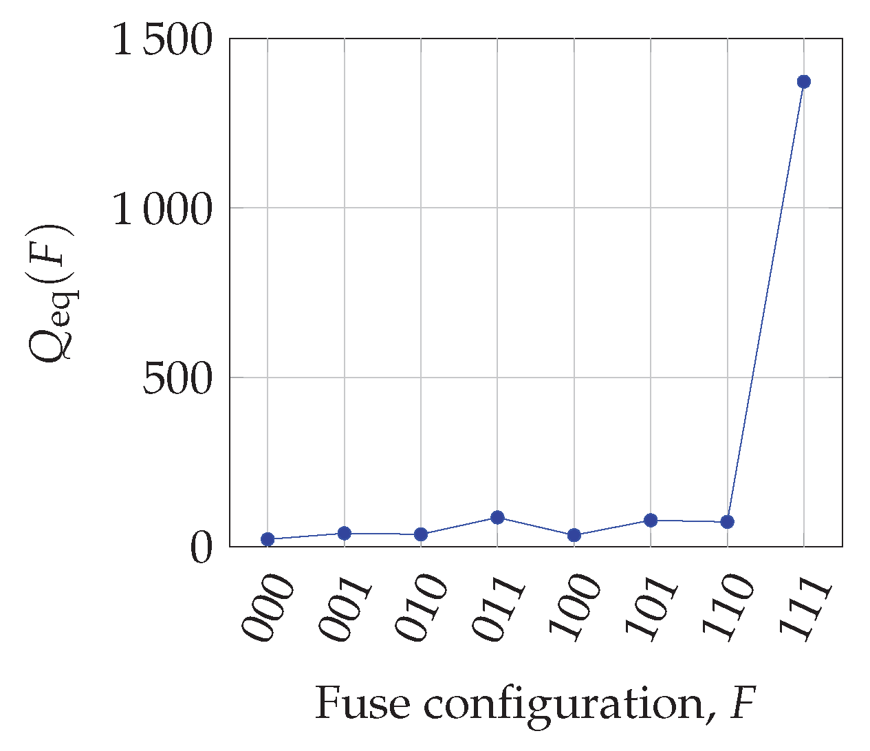
Consider an application where we need a base capacitance, C, of 3 and a trim capacitance, , of 1 with a 3-bit resolution and at an operating frequency of 433 . We thus use the circuit in Figure 1 and choose according to Equation (3). The resolution is thus . The question arises on how to select the scaled fuse resistance for the different fuses, . Consider first the naive design in which all fuses have the same resistance and consist only of a single fuse whose resistance is while active and while blown. Figure 3a shows the resulting equivalent Q factor, , as a function of fuse configuration, F. Here, F is represented by a 3-bit binary number where 1 signifies an active fuse and 0 signifies that a fuse is blown. While the best-case Q factor is high at , the worst-case Q factor is much lower at .
A more balanced equivalent Q factor can be achieved if Equations (16) and (17) are used to obtain an expression for the scaled fuse resistance, . Using these equations, we get
Figure 3b shows the resulting Q factor, , as a function of F. It can be seen from the figure that the Q factor is constant independent of fuse configuration and that the worst-case Q factor has been increased to , a 72 increase compared to the naive design. Note that, as expected, this value for coincides with the value at the intersection point of Figure 2.
The improvement results from the fact that we have identified that some configurations yield a much higher Q factor than others and made appropriate adjustments. By sacrificing the Q factor of the good configurations we have increased it for the worse ones resulting in a better Q factor for the worst case. The variation of the Q factor from 114 to 297 has been reduced to no variation at all.
Because of the potential high fuse count, it may be impractical to realise the values for in Equations (34)–(36) to a high degree of accuracy with a series/parallel combination of a single fuse resistance, . However, the following combinations yield values that are within 6% of the desired ones using only one or two fuses for each branch:
Figure 3c shows the resulting equivalent Q factor, . The worst-case value has now decreased to , a 5% decrease compared to the ideal design. A result of this deviation from the ideal is that the Q factor is once again not completely constant.
The number of bond pads required to be able to blow all fuses amounts to 6 because there are a total of 5 fuses in the circuit and one additional bond pad for the current return path is required. Standard-size bond pads for a 180 process present a capacitance to ground around of 140 per pad. The total amount of capacitance from bond pads would thus be much larger than and we would need to consider a different approach. Scaling down the pad area to , probe pads with a capacitance of approximately per pad can be manufactured. Using such pads to program the fuses results in a total parasitic capacitance contribution from pads of maximum 21 , which is about a factor of 7 smaller than the resolution, . The variation in capacitance due to the non-ideal Q factors of the trim branches amounts to 344 , close to the ideal case of 312 , calculated from Equation (26), which is far below the intended resolution.
In the previous example, the worst-case Q factor for the naive design is smaller than that for the practical design, however, not by a huge factor. This is because the process parameters, and , the desired base and trim capacitances, C and , number of bits, m, as well as the operating frequency happen to be of values which are beneficial for high Q factors. Consider what would happen if both specified capacitances, C and , are decreased by a factor of 10. Equations (16) and (17) show that significantly larger values would be needed for the scaled fuse resistance, . Figure 4 shows the equivalent Q factor, , as a function of fuse configuration, F, for and . Interestingly, identical graphs would be produced if either the operating frequency or and were decreased by a factor of 10 instead of C and . From the figure, it can be seen that the fuse configuration achieves a much more favourable Q factor than the other configurations, with . The worst-case Q factor is significantly lower at . Relating to Figure 2, the reason for this behaviour is that the fuse scaling factor, , for each fuse is not high enough and the operating point ends up to the left of the intersection point yielding very high Q factors for active fuses, but very low ones for blown fuses. Coming back to Figure 4, we see that only the case for all fuses active yields a high Q factor. By scaling the fuses appropriately and because the maximum worst-case Q factor is frequency-independent and constant for constant and , we can again achieve the Q factors of Figure 3b with a worst-case (and best-case) Q factor of .
To illustrate what could happen if care is not taken to ensure a sufficiently high Q factor, consider what would happen if a state-of-the art coil was to be used with the capacitor from the last example to form an LC resonator. Q factors of on-chip coils of [2] and [3] operating at hundreds of have been demonstrated. Connecting one such coil to a capacitor with a worst-case Q factor of , as in the example, the worst-case Q factor of the resulting LC circuit would be reduced by over 30% compared to the original Q factor of the coil. However, if the method described in this work was to be used, the coils could be connected to a capacitor with a worst-case Q factor of 187 as in Figure 3c, reducing the worst-case Q factor of the resulting LC circuit by less than 6%.
Another challenge arises when we attempt to implement a practical circuit approximating the ideal design for this case of smaller capacitances. For instance, the highest resistance we would need to realise is for which 21 fuses would be needed. Such a circuit would require around 40 bond or probe pads which would present a relatively large parasitic pad capacitance, 140 in the worst case, to the trim capacitor, limiting the resolution. Since the desired resolution is even less than that at 100 , the circuit designers should consider accepting a lower resolution, reducing the number of bits and/or reducing the base capacitance, C.
The requirement of high numbers of series fuses arises when the largest scaled fuse resistance, , becomes much larger than . Equations (16) and (17) show that this occurs when
Thus, for higher frequencies, larger specified capacitances, larger fuse resistances or a fewer number of bits than for the previous example, a high number of series fuses would not be an issue. In this case, most fuses will be required in parallel instead, to achieve sufficiently low values for .
5. Conclusions
In this paper, we present a circuit implementing a fuse-based IC trimmable capacitor. A theory is presented on how to choose fuse resistances in order to achieve the highest possible worst-case Q factor for the capacitor. One advantage of a fused-based approach is that it is cheaper than the alternative method of laser trimming. The theory presented in this work is novel in that, to the authors’ knowledge, high-Q, fuse-based trimmable IC capacitors have not previously been published.
We show that proper selection of fuse resistances not only maximises the worst-case Q factor, but also makes it constant and independent of fuse configuration. This makes it possible to build applications such as on-chip tunable LC resonant circuits with a predictable Q factor that is independent of tuned frequency without resorting to laser trimming.
Furthermore the accuracy of the capacitance is discussed and it is concluded that capacitance from bond pads may be a limiting factor. This limitation can to some extent be overcome by the use of smaller, low capacitance probe pads.
Author Contributions
Conceptualization, J.N., J.B. and J.J.; Data curation, J.N.; Formal analysis, J.N.; Funding acquisition, J.B. and J.J.; Methodology, J.N.; Project administration, J.J.; Supervision, J.B. and J.J.; Visualization, J.N.; Writing—original draft, J.N.; Writing—review & editing, J.N., J.B. and J.J.
Funding
This research was funded by Svenska Kraftnät, grant number 2013/734.
Conflicts of Interest
The authors declare no conflict of interest. The founding sponsors had no role in the design of the study; in the collection, analyses, or interpretation of data; in the writing of the manuscript, or in the decision to publish the results.
References
- Olmos, A. A temperature compensated fully trimmable on-chip IC oscillator. In Proceedings of the 16th Symposium on Integrated Circuits and Systems Design (SBCCI 2003), Sao Paulo, Brazil, 8–11 September 2003; pp. 181–186. [Google Scholar] [CrossRef]
- Zargham, M.; Gulak, P. Fully Integrated On-Chip Coil in 0.13 μm CMOS for Wireless Power Transfer through Biological Media. IEEE Trans. Biomed. Circuits Syst. 2015, 9, 259–271. [Google Scholar] [CrossRef] [PubMed]
- Feng, P.; Yeon, P.; Cheng, Y.; Ghovanloo, M.; Constandinou, T.G. Chip-Scale Coils for Millimeter-Sized Bio-Implants. IEEE Trans. Biomed. Circuits Syst. 2018, 12, 1088–1099. [Google Scholar] [CrossRef] [PubMed]
- Nilsson, J.; Borg, J.; Johansson, J. Single chip wireless condition monitoring of power semiconductor modules. In Proceedings of the Nordic Circuits and Systems Conference (NORCAS): NORCHIP International Symposium on System-on-Chip (SoC), Oslo, Norway, 26–28 October 2015; pp. 1–4. [Google Scholar] [CrossRef]
- Nilsson, J.; Borg, J.; Johansson, J. Chip-coil design for wireless power transfer in power semiconductor modules. In Proceedings of the 2018 2nd Conference on PhD Research in Microelectronics and Electronics Latin America (PRIME-LA), Puerto Vallarta, Mexico, 25–28 Febraury 2018; pp. 1–4. [Google Scholar] [CrossRef]
- Gabriel, C. Compilation of the Dielectric Properties of Body Tissues at RF and Microwave Frequencies; Technical Report; King’s College London (United Kingdom), Department of Physics: London, UK, 1996. [Google Scholar]
- International Telecommunications Union. Radio Regulations; International Telecommunications Union: Geneva, Switzerland, 2016; Chapter 1. [Google Scholar]
- Cohen, M.I.; Unger, B.A.; Milkosky, J.F. Laser Machining of Thin Films and Integrated Circuits. Bell Syst. Tech. J. 1968, 47, 385–405. [Google Scholar] [CrossRef]
- Sjöblom, P.; Sjöland, H. Measured CMOS Switched High-Quality Capacitors in a Reconfigurable Matching Network. IEEE Trans. Circuits Syst. II Express Briefs 2007, 54, 858–862. [Google Scholar] [CrossRef]
- Ding, S.J.; Hu, H.; Zhu, C.; Kim, S.J.; Yu, X.; Li, M.F.; Cho, B.J.; Chan, D.S.H.; Yu, M.B.; Rustagi, S.C.; et al. RF, DC, and reliability characteristics of ALD HfO2-Al2O3 laminate MIM capacitors for Si RF IC applications. IEEE Trans. Electron Devices 2004, 51, 886–894. [Google Scholar] [CrossRef]
- Flandre, D.; de Wiele, F.V. A new analytical model for the two-terminal MOS capacitor on SOI substrate. IEEE Electron Device Lett. 1988, 9, 296–299. [Google Scholar] [CrossRef]
Figure 1.
Fuse-based trimmable capacitor.

Figure 2.
Q factor, , for a 3 capacitor in parallel with a series combination of a fuse and a 1 capacitor, plotted as a function of fuse scaling factor, . is plotted for both active and blown fuses corresponding to different fuse resistances. Plots for manufactured capacitors with both infinte Q factors and Q factors of 10000 are shown, with the latter case in a lighter shade.

Figure 3.
Equivalent Q factor, , of a trimmable capacitor of and , operating at 433 as a function of the configuration of 3 fuses, represented by a binary number, F, where the nth bit represents fuse n, . signifies an active fuse, while = 0 signifies that fuse n is blown. Plots are shown for three designs: (a) The naive design, where all fuses have the same resistance, ; (b) The ideal design, where all fuses have been scaled to their optimal resistance ; and (c) The practical design, where all the fuses consist of series/parallel combinations of one or two fuses of resistance in order to approximate .

Figure 4.
Equivalent Q factor, , of a trimmable capacitor as a function of the configuration of 3 fuses with the same resistance, . All parameters are the same as in Figure 3a, except the specified capacitances, C and , have both been decreased by a factor of 10.
Figure 4.
Equivalent Q factor, , of a trimmable capacitor as a function of the configuration of 3 fuses with the same resistance, . All parameters are the same as in Figure 3a, except the specified capacitances, C and , have both been decreased by a factor of 10.

© 2019 by the authors. Licensee MDPI, Basel, Switzerland. This article is an open access article distributed under the terms and conditions of the Creative Commons Attribution (CC BY) license (http://creativecommons.org/licenses/by/4.0/).
Share and Cite
MDPI and ACS Style
Nilsson, J.; Borg, J.; Johansson, J. Maximal Q Factor for an On-Chip, Fuse-Based Trimmable Capacitor. Electronics 2019, 8, 62. https://doi.org/10.3390/electronics8010062
AMA Style
Nilsson J, Borg J, Johansson J. Maximal Q Factor for an On-Chip, Fuse-Based Trimmable Capacitor. Electronics. 2019; 8(1):62. https://doi.org/10.3390/electronics8010062
Chicago/Turabian StyleNilsson, Joakim, Johan Borg, and Jonny Johansson. 2019. "Maximal Q Factor for an On-Chip, Fuse-Based Trimmable Capacitor" Electronics 8, no. 1: 62. https://doi.org/10.3390/electronics8010062
Note that from the first issue of 2016, this journal uses article numbers instead of page numbers. See further details here.