Article

Additive Manufacturing of Monolithic Microwave Dielectric Ceramic Filters via Digital Light Processing

1
College of Mechanical and Electrical Engineering, Nanjing University of Aeronautics and Astronautics, Nanjing 210016, China
2
Department of Engineering and Design, University of Sussex, Sussex House, Brighton BN1 9RH, UK
3
Nanjing Institution of Advanced Laser Technology, Nanjing 210038, China
*
Author to whom correspondence should be addressed.
Electronics 2019, 8(10), 1067; https://doi.org/10.3390/electronics8101067
Submission received: 26 August 2019 / Revised: 16 September 2019 / Accepted: 18 September 2019 / Published: 20 September 2019
(This article belongs to the Special Issue Filter Design Solutions for RF systems)

Abstract

:
Microwave dielectric ceramics are employed in filters as electromagnetic wave propagation media. Based on additive manufacturing (AM) techniques, microwave dielectric ceramic filters with complex and precise structures can be fabricated to satisfy filtering requirements. Digital light processing (DLP) is a promising AM technique that is capable of producing filters with high accuracy and efficiency. In this paper, monolithic filters made from Al2O3 and TiO2, with a molar ratio of 9:1 (0.9 Al2O3-0.1 TiO2), were fabricated by DLP. The difference in the dielectric properties between the as-sintered and post-annealed samples at different temperatures was studied. The experimental results showed that when sintered at 1550 °C for 2 h and post annealed at 1000 °C for 5 h, 0.9 Al2O3-0.1 TiO2 exhibited excellent dielectric properties: εr = 12.4, Q × f = 111,000 GHz, τf = +1.2 ppm/°C. After comparing the measured results with the simulated ones in the passband from 6.5 to 9 GHz, it was concluded that the insertion loss (IL) and return loss (RL) of the filter meet the design requirements.

1. Introduction

In recent years, microwave dielectric ceramics have shown great advantages in the development of miniaturization, weight reduction, and integration of filters [1]. Low dielectric constant microwave dielectric ceramics have fast transmission and response speed, high temperature stability in working environment, high signal transmission quality, low transmission loss, and good frequency selectivity. Owing to these superior qualities, they are widely used in 5G wireless mobile communication, satellite communication, and radar systems.
When the microwave dielectric ceramic is employed on equipment with high communication quality, it is necessary to have a small dielectric constant εr, a quality factor Q as large as possible, and a frequency temperature coefficient τf of near zero in order to meet the requirements of the application. Actually, the microwave communication device is used at different temperatures. If the resonant frequency of the microwave dielectric material changes greatly with temperature, the carrier signal will drift at different temperatures, thereby affecting the performance of the device. It is required that the resonant frequency of the material should hardly change with temperatures. Mg2SiO4, Mg4Nb2O9, and Al2O3 are widely studied as common low dielectric constant microwave dielectric ceramics, though the Q × f value of Al2O3 is significantly higher than that of Mg2SiO4 and Mg4Nb2O9 [2]. As a typical low dielectric constant microwave dielectric ceramic, Al2O3 possesses the qualities of low manufacturing cost, high precision and great thermal conductivity (i.e., 24.5 W m−1 K−1 at room temperature) [3]. Above all, it exhibits outstanding dielectric properties at millimeter wave frequency. Alford reported the microwave dielectric properties of Al2O3: εr = 10, Q × f = 500,000 GHz, and τf = −60 ppm/°C [4]. However, it also has obvious disadvantages. As mentioned above, the τf of Al2O3 is relatively large and the sintering temperature is quite high (1600 °C to 1700 °C), limiting its industrial application. At the same time, TiO2 ceramics have a εr of 100, a Qf of 48,000 GHz, and a positive large τf of + 450 ppm/°C [5]. Therefore, in order to improve the dielectric performance of Al2O3 ceramics, a certain amount of TiO2 is usually added to form Al2O3-TiO2 composite ceramics, allowing a value of τf tending to zero to be obtained. Youshihiro et al. have reported the dielectric properties of the Al2O3-TiO2 system, of which τf is nearly zero when the molar ratio of Al2O3 to TiO2 is 9:1 [6]. Due to different working temperatures, the thermal conductivity of the Al2O3-TiO2 system is a problem that needs to be considered. Generally, high thermal conductivity of typical ceramics can be correlated to common features like simple crystal structure, low atomic mass, strong interatomic forces, high atomic packing density, comparable atomic weight differences among the components in the composition, etc. Moreover, the thermal conductivity has a reciprocal relation with the square root of mean atomic mass in the material [7]. It is worth noting that the elements in 0.9 Al2O3-0.1 TiO2 system possess relatively low atomic weight. The melting temperature of 0.9 Al2O3-0.1 TiO2 is around 1900 °C, which is an indirect indicator of strong interatomic bonding, a prerequisite for high thermal conductivity.
Nowadays, microwave and radio frequency passive devices realized by additive manufacturing (AM) have attracted an increasing amount of attention [8,9,10]. Different materials can be manufactured via AM, including plastics, metals, and ceramics. The latter has been widely used in filters as dielectric resonators. For components made entirely of ceramics, their surface metalization is achieved by employing electroless nickel/copper plating, thereby avoiding the radiation of the electromagnetic field [11]. A remarkable advantage of AM compared to traditional computer numerical control (CNC) milling technology, is that the processed object is accumulated layer by layer, and the processing cost is theoretically only related to the volume of the object (i.e., the amount of raw materials) and does not consider the complexity of its geometric structure. Therefore, in terms of complex geometric structures, the cost of AM is lower than that of traditional CNC milling technology, making AM technology particularly suitable for manufacturing complex and precise mechanical structures. Typically, molding accuracy and efficiency are unable to be simultaneously achieved, particularly for AM methods. The technique of point-by-point scanning molding using 3D Gel Printing (3DGP) and stereolithography (SLA) methods requires a significant amount of shaping time [12]. Digital light processing (DLP) based on the surface exposure AM method can theoretically avoid this shortcoming and does not require scanning path planning [13,14]. Compared with other AM methods, DLP has the characteristics of high precision, small internal size, and fast forming speed. Our team has successfully fabricated bone scaffolds using bio-ceramic material hydroxyapatite via DLP AM technology, which demonstrated the feasibility of the DLP method in manufacturing ceramic materials [15]. This study utilizes DLP AM technology to fabricate microwave dielectric ceramic filters to significantly improve the forming efficiency while also ensuring accuracy.
In this paper, a ceramic suspension with suitable viscosity was prepared using photopolymer, Al2O3, and TiO2 powders. The designed monolithic microwave dielectric ceramic filter was fabricated by DLP technology. The filter sample was then obtained after post treatment processes, including drying, debinding, sintering, post annealing, and metalization. The effects of sintering temperature and annealing process on the dielectric properties of 0.9 Al2O3-0.1 TiO2 ceramics were investigated based on the densification, X-ray diffraction (XRD), and microstructure of the samples. The S-parameters and group delay obtained from the actual test were compared with the simulation results, indicating that the manufactured filter meets the design requirements. The research results show that it is feasible to make sophisticated microwave dielectric ceramic filters using DLP AM technology.

2. Materials and Methods

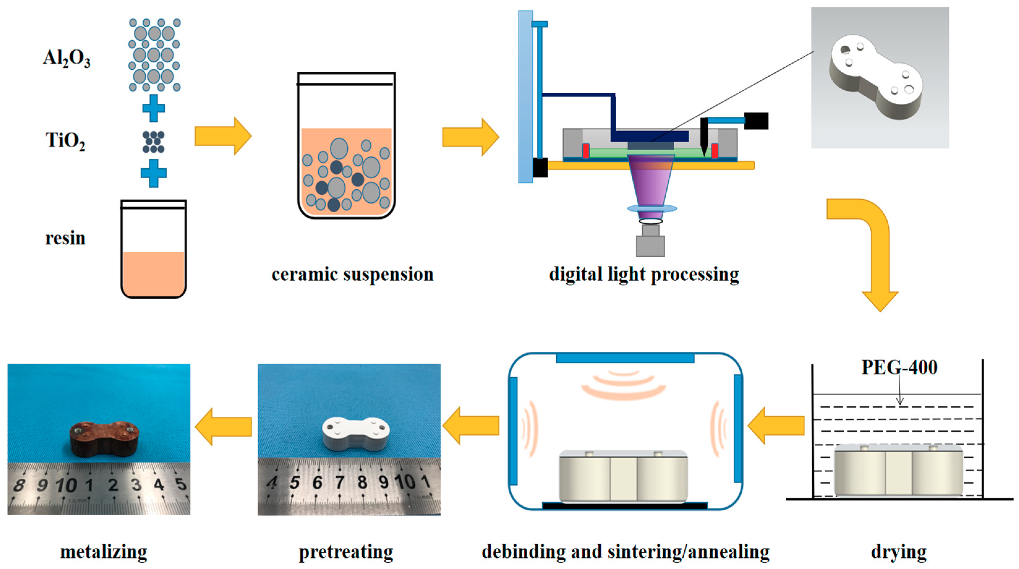
2.1. Preparation of the Ceramic Suspension

Figure 1 shows the complete preparation of the microwave dielectric ceramic filter. In this study, a micro-sized, nano-sized spherical Al2O3 powder and micro-sized spherical TiO2 powder (Al2O3 ≥ 99.9 wt%, TiO2 ≥ 99.5 wt%, Chengdu Kewan Intelligent Technology Co., Ltd, Chengdu, China) were used as the starting material with a particle size of 5 mm, 500 nm, and 1 μm, respectively. Table 1 lists the basic physical parameters of the three powders. The Al2O3 powder of two particle sizes is uniformly mixed at a 1:1 wt ratio, followed by the TiO2 powder being added to the mixed Al2O3 powder at a molar wt ratio of 1:9. The premixed solution used to prepare the ceramic suspension consisted of two components: photosensitive resin (Shanghai Ai Rui Technology Co., Ltd, Shanghai, China) and sodium polyacrylate dispersant (Hebei Jinghong Chemical Co., Ltd, Hebei, China). The as-prepared powder was then added to the premixed solution to form the ceramic suspension. After manual premixing, the ceramic suspension was then ball-milled for 12 h using zirconia balls. The suspension was then degassed for 30 min using a vacuum mixer. In this way, a ceramic suspension with solid content of 45% could be obtained. In this work, the mixing of the nanopowders and the micropowders was performed in order to create a balance between the viscosity of the ceramic slurry and the density of the sintered body. Previous theoretical and experimental studies have demonstrated that the combination of powders with different particle sizes is an effective method for increasing the volume fraction and reducing the viscosity of the ceramic slurry. Moreover, the density of the sintered body made of powders of different particle sizes is higher than that made of a single particle size powder [16].

2.2. Design and Simulation of the Microwave Dielectric Ceramic Filter

As depicted in Figure 2a, a two-pole transverse magnetic (TM) mode microwave dielectric ceramic filter, in which the fundamental resonance is the TM01δ mode, was designed with the following parameters. The center frequency was 8.3 GHz and fractional bandwidth was 1.54%. The height of the filter was 10 mm, whereas the radius of the cylindrical cavity was 7.58 mm. The diameter of the two center posts, acting as resonators, was 3 mm. The thickness of the chamber wall was set to 1 mm, which is convenient for manufacturing and microwave performance testing. Alignment posts were designed to facilitate the placement of Sub-Miniature version A (SMA) connectors for the input and output couplings. After designing the size parameters of the filter, a High Frequency Structure Simulator (HFSS) was utilized for simulation, which is based on the finite element method (FEM). The essential steps are listed below.
(1)
The geometric model of the filter was first created using 3D Modeler according to the size parameters of the design, which are shown in Figure 2b.
(2)
The microwave dielectric material selected in the design was set to have a εr of 12.4.
(3)
According to the defined port and boundary conditions, excitation type was a lumped port excitation, boundary type was set to be Perfect E.
(4)
Then the simulation frequency range needed to be defined. The center frequency of the designed filter was 8.3 GHz, and the simulation frequency range was 6.5–9 GHz.
(5)
After the above operations, the simulation step was run.

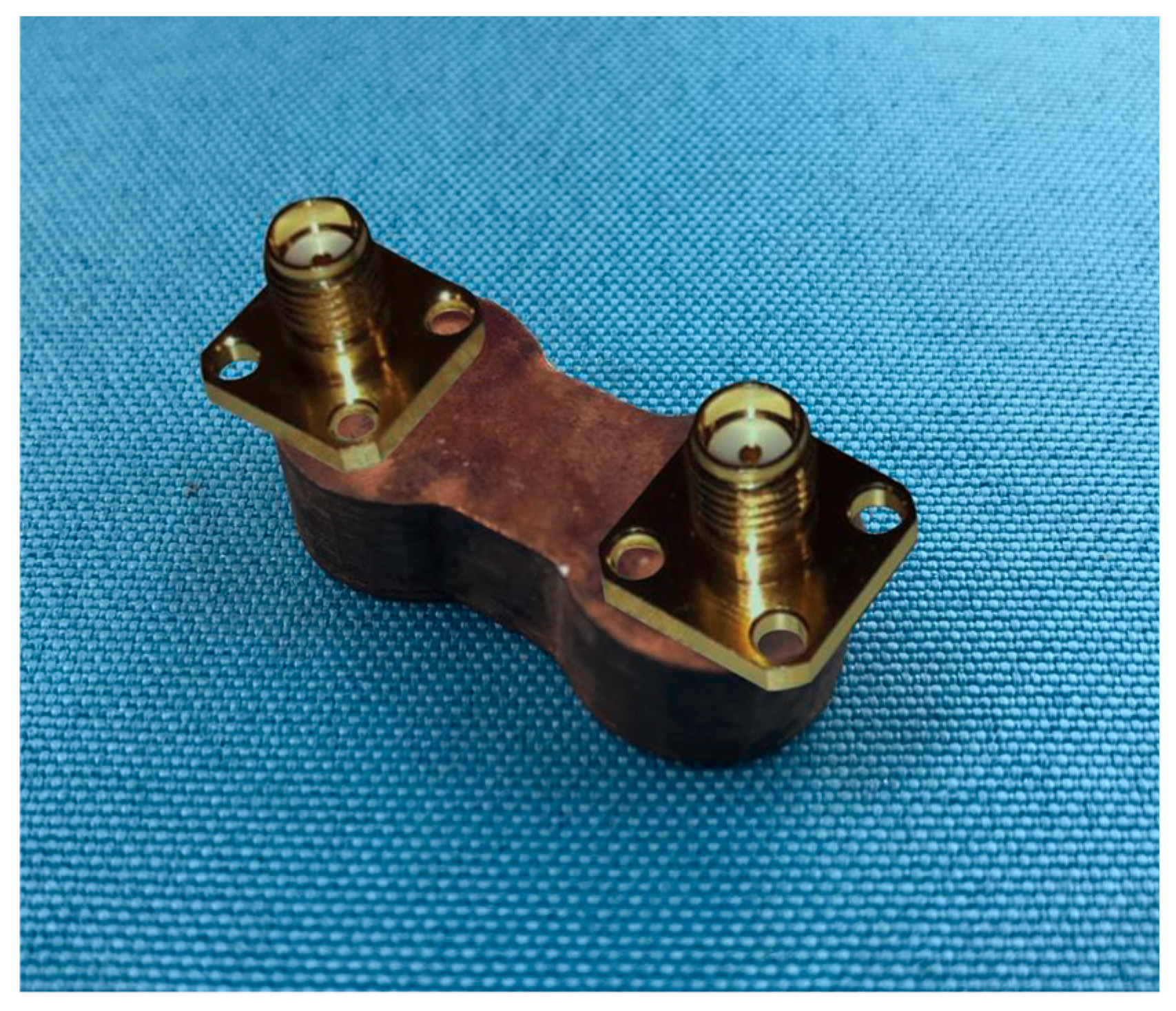
2.3. Fabrication and Post Treatment of the Filters

Firstly, the 3D model was created using the Unigraphics NX (UG) software (Siemens PLM Software, Plano, TX, USA), and then the Magics software was employed to generate the supporting structure and to slice the parts. The final data was output as a stereolithography (STL) file, which was then imported into the DLP printer. The DLP printing machine was developed by the Nanjing University of Aeronautics and Astronautics. The light source of the DLP printer can emit ultraviolet light at a wavelength of 405 nm. The size of the experimental molding substrate was 60 mm × 80 mm, and its z axis accuracy was 10 μm. As shown in Figure 3, selective scanning of the ceramic suspension by ultraviolet light during the molding process cures each layer pattern. After the first layer is cured, the forming platform moves upward and the ceramic suspension was recoated on the cured surface with a blade. The second layer is then cured using the same process. These steps are repeated until the entire ceramic body is finally obtained.
The printed ceramic body then underwent ultrasonic cleaning in alcohol, followed by running tap water. After that, the residual water in the body had to be removed by drying. An innovative method is to use PEG-400. For the PEG-based extraction process, the sample was immersed in PEG-400, which was expected to result in a uniform extraction rate in all directions [17]. With the purpose of removing the polymer binder and achieving densification, the sample then underwent two thermal processes: debinding and sintering. A two-step debinding method was adopted in this work. The first stage under vacuum debinding was to slow down the pyrolysis rate, and a second debinding in the air was conducted to ensure complete removal of residual carbon. The debinding stage is the most time-consuming step since the resin needs to be slowly removed to prevent cracking. As shown in Figure 4, according to the phase diagram of Al2O3-TiO2, the two reacted at 1200 °C to form the Al2TiO5 phase. The appearance of Al2TiO5 depreciates the properties of Al2O3-TiO2 microwave dielectric ceramics [6]. Accordingly, the annealing process is required to eliminate the adverse effects of Al2TiO5. The binder-removed samples were sintered at temperatures of 1450 °C, 1500 °C, 1550 °C, and 1600 °C. They were then kept at the highest temperature for 2 h, and then annealed at 1000 °C for 5 h. The sintered 0.9 Al2O3-0.1 TiO2 ceramic part shrinks, and the shrinkage coefficient of the sample was measured to be approximately 25%. This signifies that the original model must be scaled up accordingly before manufacturing. In order to shield the filter, a 10 μm copper layer was applied to the external surfaces.

2.4. Measurements and Characterizations

The microstructure of the sintered sample was characterized by scanning electron microscope (SEM) (S-4800; Hitachi Instruments, Tokyo, Japan). The relative density was determined by the Archimedes’ displacement method. The samples at different temperatures were investigated by XRD (DMAX2500PC; Rigaku Corp., Tokyo, Japan) under the following conditions: 10°–80° diffraction angle, CuKα radiation (λ = 1.5406 Å), 40 kV, 100 mA, 0.02° step width, and 5°/min scanning speed. Qf and εr were measured by a network analyzer (Agilent 8722E) (Keysight, Santa Rosa, CA, USA) using a pair of parallel conducting Ag and Cu plates in the TE011 mode of modified Hakki and Coleman’s resonator method [18,19]. The Agilent 8722ET network analyzer and incubator were used to measure τf at the temperature range of 20 °C–80 °C. The calculation formula is:
τ f = 1 f 20 f 80 f 20 80 20
in which f80 and f20 are the resonant frequencies at 80 °C and 20 °C, respectively. The designed microwave dielectric ceramic filter was simulated by HFSS, and its insertion loss, return loss, and group delay were obtained. As shown in Figure 5, two SMA connectors were mounted on the fabricated filter structure to enable testing of their microwave performance with the network analyzer (Keysight N5247A) (Keysight, Santa Rosa, CA, USA).

3. Results

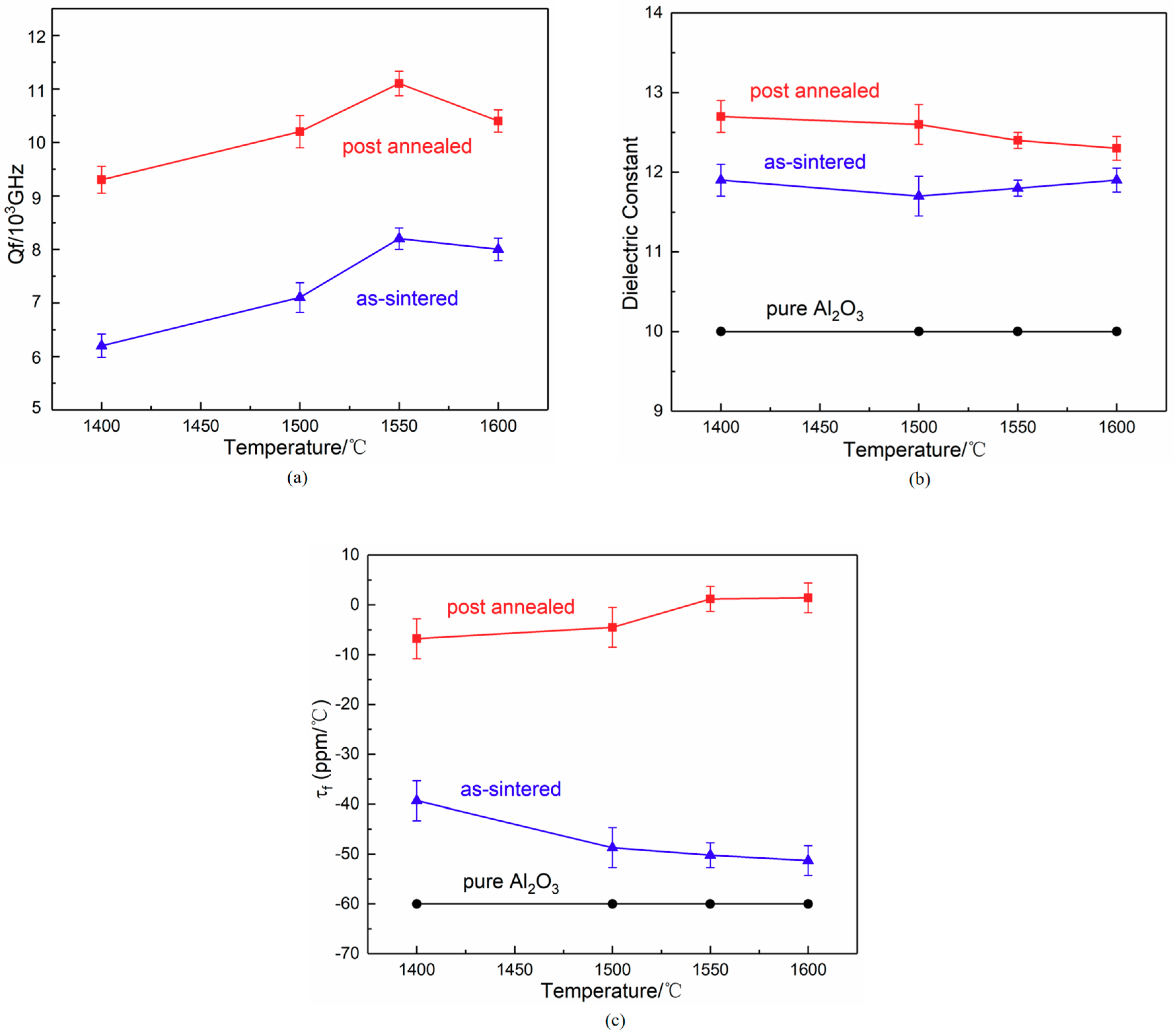
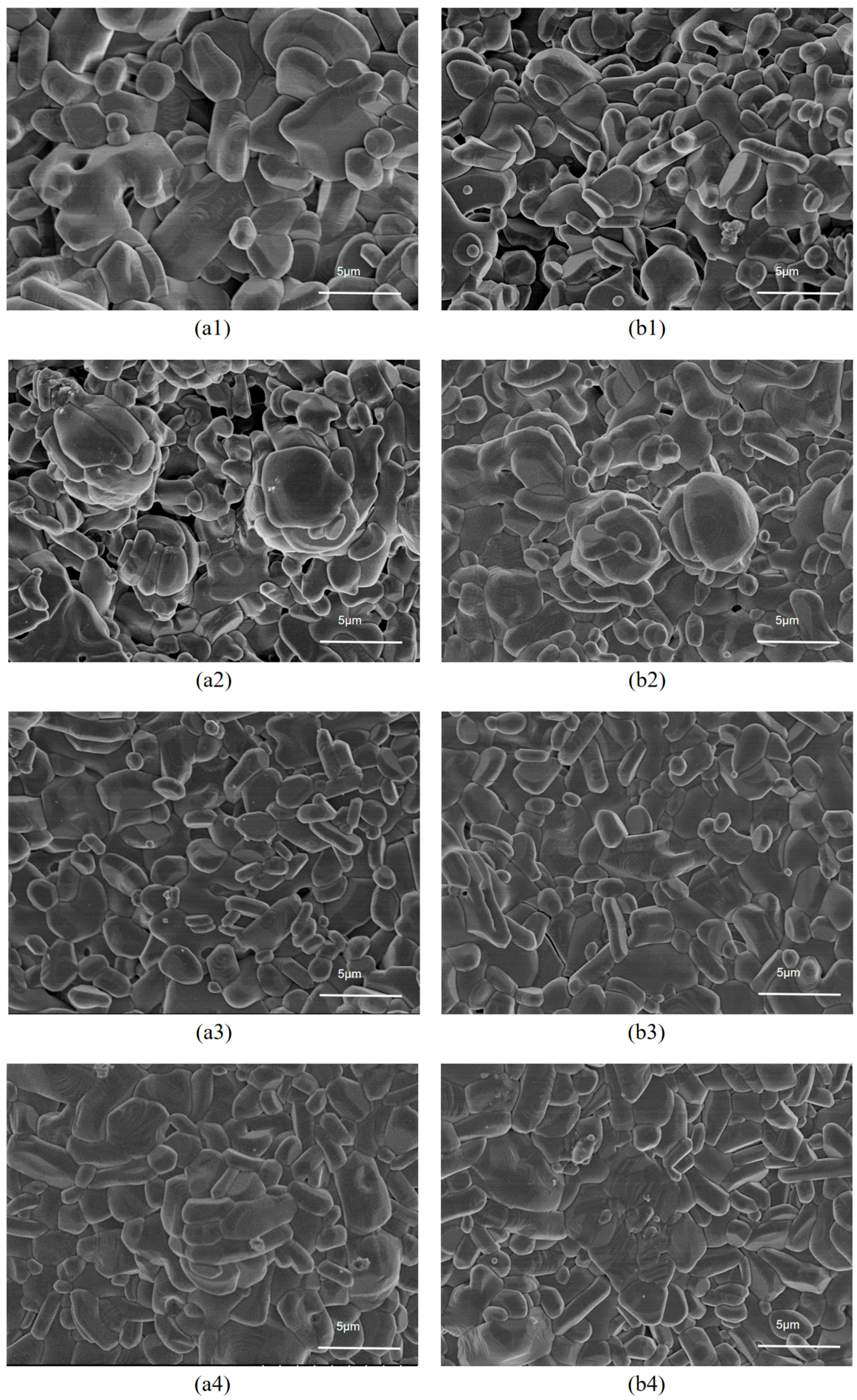
3.1. The Results of the Dielectric Properties

Figure 6 shows the changing trend in the dielectric properties of the 0.9 Al2O3-0.1 TiO2 system, and Table 2 lists the accurate values of the 0.9 Al2O3-0.1 TiO2 system before and after annealing at different sintering temperatures. As shown in Figure 6a, with the increase in sintering temperature, the Qf value of the 0.9 Al2O3-0.1 TiO2 ceramics first increases and then decreases, reaching a maximum at 1550 °C. However, the post-annealed sample had an increase of about 30,000 GHz in Qf value compared to the as-sintered sample at the same temperature. From the point of view of ceramic technology, as long as there exists consistent structure, high density, and uniform grain growth, impurities and defects are reduced. As such, the dielectric loss tanδ can be reduced, thus resulting in an improved Q value. In the Discussion section, dielectric properties will be analyzed based on the relative density, microstructure, and crystal structure of the sample.
Figure 6b shows that the εr of the 0.9 Al2O3-0.1 TiO2 system is larger than that of the pure Al2O3, while the εr of the post-annealed sample is increased compared with the as-sintered sample. It can be seen from Table 2 that the dielectric constant of the 0.9 Al2O3-0.1 TiO2 system after annealing at different temperatures is essentially unchanged, all are around 12.5.
Figure 6c shows the variation of the τf of the 0.9 Al2O3-0.1 TiO2 system at different temperatures. With the increase in temperature, the τf of pure Al2O3 remains basically unchanged, which is approximately equal to −60 ppm/°C. The sample after annealing has a larger improvement than the as-sintered in the τf, and the value of τf differs by more than 30 ppm/°C. After annealing at 1550 °C, the τf of the sample is +1.2 ppm/°C, which is the closest to zero.

3.2. The Results of S Parameters and Group Delay of the Filter

The aforementioned dielectric properties of 0.9 Al2O3-0.1 TiO2 at different temperatures indicates that when sintered at 1550 °C for 2 h and annealed at 1000 °C for 5 h, the composite material exhibits the best performance. The DLP-manufactured filter was treated by this process.
Figure 7a shows the differences of insertion loss (IL) and return loss (RL) of the microwave dielectric ceramic filter between the actual measurement and electromagnetic simulation. The center frequency of the filter was set to be 8.3 GHz in the electromagnetic simulation whereas the measured center frequency deviates from the center frequency by 0.05 GHz, that is the ∆f = 0.6%. As shown in Figure 7a, the IL in the passband of 8.24–8.37 GHz in the actual measurement is 1.16–2.52 dB, which is 1.15–2.49 dB higher than the simulated one. The measured S11 curve shows that the RL is greater than 30 dB in the passband, meeting the performance specifications required for this type of filter. The passband group delay of the filter is plotted in Figure 7b. The actual measurement results show that the group delay in the 3 dB bandwidth (8.24–8.37 GHz) of the passband is 0.87–1.48 ns. Figure 7c indicates that it has good isolation and output RL in actual measurement.

4. Discussion

4.1. Discussion of the Dielectric Properties

The quality of the microstructure has a great influence on the dielectric properties of microwave dielectric ceramics. Figure 8(a1) shows that when the sintering temperature is 1400 °C, the as-sintered sample has different grain sizes and no obvious grain boundaries. However, as is shown in Figure 8(b1), the grains of the annealed sample are improved and the surface pores are reduced. When the sintering temperature rises, the grain size tends to be uniform and the surface pores gradually reduce in number and size. When the sintering temperature rises to 1600 °C, some grains are excessively grown due to over burning. It can be observed in Figure 8(a3,b3) that when the sample is sintered at 1550 °C for 2 h and annealed at 1000 °C for 5 h, the surface is regular, the grain distribution is uniform, the pores on the surface are small, and the grain boundaries are more obvious. This further verified that the 0.9 Al2O3-0.1 TiO2 system shown in Figure 6 has the best dielectric properties when sintered at 1550 °C for 2 h and post annealed at 1000 °C for 5 h.
The Qf value of 0.9 Al2O3-0.1 TiO2 first increases and then decreases with the increase in the sintering temperature, which is the result of increasing density and the appearance of secondary phase Al2TiO5. The Qf value of TiO2 is 500,000 Hz, which is one order of magnitude lower than that of Al2O3 (Qf = 5,000,000 Hz). The 0.9 Al2O3-0.1 TiO2 system can be regarded as adding TiO2 to the Al2O3 system. Firstly, with the addition of TiO2, the Qf value of the system must be lower than the Qf value of Al2O3. As shown in Figure 9, as the sintering temperature gradually increased, the relative density of the sample becomes increasingly higher, reaching a maximum at 1550 °C. Owing to the densification of the material, the tighter the ion binding is, the more difficult the ion movement is. As such, it is difficult for ion relaxation polarization to occur. Overall, there is no polarization loss, except for the electronic and ionic elastic displacement polarization. In addition, when the material is denser, there are fewer pores, thus resulting in the smaller ionization loss caused by gas ionization in the pores. Combining the above two factors, the Qf value first increases. However, when the sintering temperature reaches 1600 °C, some individual particles grow abnormally because of over burning, causing structural defects, which is the main reason for the decrease in the Qf value. Under the joint influence of these factors, the Qf value of the 0.9 Al2O3-0.1 TiO2 system first increases and then decreases with the increase of sintering temperature.
However, the Qf value of the as-sintered sample is lower than that of the annealed one at the same temperature. The reason for this is that the formation of the high loss phase Al2TiO5 reduces the Qf value of the system. It can be observed in Figure 10 that in addition to the diffraction peaks of the two phases of Al2O3 and TiO2, the diffraction peaks of Al2TiO5 appear at different sintering temperatures, indicating that Al2O3 reacts with TiO2 to form Al2TiO5 during sintering. The sample annealed at 1000 °C for 5 h showed only two phases of Al2O3 and TiO2 in the XRD pattern, signifying that the Al2TiO5 phase was decomposed by annealing treatment. According to Figure 4, when the 0.9 Al2O3-0.1 TiO2 system was sintered at 1450 °C, 1500 °C, 1550 °C, and 1600 °C for 2 h, and annealed at 1000 °C for 5 h, the composition of the phases was roughly the same.
Since εr = 10 of Al2O3 and εr = 100 of TiO2, the εr of the system is bound to increase with the addition of TiO2. As shown in Figure 4, when the sintering temperature is higher than 1200 °C and annealing is not performed, the secondary phase Al2TiO5 is formed in the 0.9 Al2O3-0.1 TiO2 system. However, the εr value of the Al2TiO5 is 3.4, which is lower than that of the main phase. Annealing at 1000 °C for 5 h results in the decomposition of Al2TiO5 with low εr and the precipitation of TiO2 with high εr, so the εr of the annealed sample is increased compared to the as-sintered one.
According to microscopic analysis, the εr is a macroscopic physical quantity that comprehensively reflects the polarization behavior of the dielectric. When the polarizing ability of the dielectric under the electric field is stronger, the εr is larger. By Clausius equation
P = N α E i
where P: macroscopic polarizability, α: microscopic polarizability, N: number of molecules per unit volume of dielectric, Ei: effective electric field, and E: average macroscopic electric field. So:
ε r = 1 + N α ε 0 E i E
It can be estimated from Formula (3) that there are three ways to increase εr. The first method is to increase the value of N, that is, to increase the density of the dielectric materials. The second method is to adopt dielectric materials composed of plasmids that have a large polarization α. The last method is by selecting material that have a large effective electric field Ei. The εr of the Al2O3 system mainly depends on the ion polarization, which is predominantly determined by the polarization mode of the lattice vibration. According to RD Shannon [20], the polarizability of Al3+ ions is 0.78 × 10−40 C·m2·V−1, and the polarization of Ti4+ ions is 2.94 × 10-40 C·m2·V−1, which further proves that the introduction of Ti4+ ions will increase the εr of the 0.9 Al2O3-0.1 TiO2 system.
The εr of the material satisfies the formula:
1 ε r = 1 ε g + 1 R ε g b ,
where εg and εgb are the dielectric constants of the grain and the grain boundary layer, respectively, and R is the ratio of the thickness of the grain to grain boundary layer (Dg/Dgb). It can be determined from Figure 8 that as the sintering temperature increases, the pores decrease and the unit cell volume increases, which is beneficial to the intracellular ion vibration. Further, the polarization is enhanced, resulting in an increase in the dielectric constant εg of the grain and the dielectric constant εgb of the grain boundary layer. During the densification of the microstructure, the crystal grains grow uniformly, and the grain boundary layers become thinner, causing R to increase. According to Formula (4), εr is thereby increased.
According to the Lichnetecker Law, the τf of Al2O3 is negative, −60 ppm/°C, while the τf of TiO2 is positive, approximately 450 ppm/°C [21]. With the addition of TiO2, the τf of the system drifts positively, and τf ≈ 0 when annealed at 1550 °C. The τf value of pure Al2O3 ceramics is not affected by the sintering temperature. The τf of the as-sintered 0.9 Al2O3-0.1 TiO2 ceramics is about −45 ppm/°C, which is attributable to the reaction of TiO2 and Al2O3 at high temperature to form the second phase Al2TiO5. As a result of the reduction of TiO2 content in the system, the negative τf of Al2O3 ceramics is not corrected too much. When adopting post-annealment, the Al2TiO5 phase decomposes and the amount of TiO2 increases. The τf value of the 0.9 Al2O3-0.1 TiO2 system changes from negative to positive. As shown in Table 2, the τf value of 1.2 ppm/°C was obtained after being annealed at 1550 °C.

4.2. Error Analysis of the Simulated and Measured Results of the Microwave Dielectric Ceramic Filter

Figure 7 presents the measured results compared with the simulation results. The measured center frequency was shifted backward by 0.05 GHz, which is caused by the uncertainty of the shrinkage of the ceramic sample after debinding and sintering. According to the previous measurements, after the body was sintered, the linear shrinkage was about 25%, so the model is enlarged to 1.34 times of the original size. However, the size of the filter will deviate slightly after sintering. For example, although the actual measurement shows that the wall thickness is 1.15 mm, the wall thickness of the sintered filter is expected to be 1 mm. For such reasons, the results of the measurement may deviate from the simulation results. Compared with the simulation results, the actual measured IL and RL are a little large. This is attributable to the fact that, in addition to the manufacturing errors mentioned above, the influence of the layer thickness and quality of the metal layer on the measurement is also considered. It should be noted that this was not taken into account during the electromagnetic simulation process.

5. Conclusions

In this paper, DLP AM technology and microwave dielectric ceramic material were utilized to fabricate a monolithic microwave dielectric ceramic filter with a complex and precious structure. When sintered at 1550 °C for 2 h and post annealed at 1000 °C for 5 h, the obtained dielectric properties of the 0.9 Al2O3-0.1 TiO2 system were the best: εr = 12.4, Q × f = 111,000 GHz, and τf = +1.2 ppm/°C. The measured value of the central frequency deviates from that of the simulated central frequency by 0.05 GHz, that is, the ∆f = 0.6%. The actual IL value is 1.16–2.52 dB in the passband of 8.24–8.37 GHz and the actual RL value is greater than 30 dB, satisfying the design requirements of this type of filter. This work provides an effective method for manufacturing monolithic microwave dielectric ceramic filters with complex and precious structures, which can be widely used in cellular mobile network systems, communication base stations, television satellite receiving systems, satellite communication, and radar systems, etc. By controlling the composition of the ceramic material and improving the quality of the metalization coating, the dielectric properties of the ceramic material can be further optimized and the applicable frequency band of the filter can be further improved.

Author Contributions

Conceptualization, Q.L. and L.S.; investigation, C.J. and D.X.; methodology, Y.Y. and M.X.; writing—original draft preparation, Q.L.; writing—review and editing, C.W., M.Q. and J.Z.

Funding

This research was funded by the National Key Research and Development Program “Additive Manufacturing and Laser Manufacturing” (Grant No. 2018YFB1105400 and 2018YFB1105801), National Natural Science Foundation of China (Grant No.U1537105 and No.U1532106) and National Key Laboratory of Science and Technology on Helicopter Transmission (Nanjing University of Aeronautics and Astronautics) (Grant No. HTL-A-19G011).

Conflicts of Interest

The authors declare no conflict of interest.

References

  1. Raveendran, A.; Sebastian, M.T.; Raman, S. Applications of Microwave Materials: A Review. J. Electron. Mater. 2019, 48, 2601–2634. [Google Scholar] [CrossRef] [Green Version]
  2. Sebastian, M.T.; Ubic, R.; Jantunen, H. Low-loss dielectric ceramic materials and their properties. Int. Mater. Rev. 2015, 60, 392–412. [Google Scholar] [CrossRef]
  3. Partridge, G. Inorganic materials V. Ceramic materials possessing high thermal conductivity. Adv. Mater. 1992, 4, 51–54. [Google Scholar] [CrossRef]
  4. Alford, N.M.; Penn, S.J. Sintered alumina with low dielectric loss. J. Appl. Phys. 1996, 80, 5895–5898. [Google Scholar] [CrossRef] [Green Version]
  5. Templeton, A.; Wang, X.; Penn, S.J.; Webb, S.J.; Cohen, L.F.; Alford, N.M. Microwave Dielectric Loss of Titanium Oxide. J. Am. Ceram. Soc. 2000, 83, 95–100. [Google Scholar] [CrossRef]
  6. Ohishi, Y.; Miyauchi, Y.; Ohsato, H.; Kakimoto, K.-I. Controlled Temperature Coefficient of Resonant Frequency of Al2O3-TiO2 Ceramics by Annealing Treatment. Jpn. J. Appl. Phys. 2004, 43, 749–751. [Google Scholar] [CrossRef]
  7. Roshni, S.B.; Sebastian, M.T.; Surendran, K.P. Can zinc aluminate-titania composite be an alternative for alumina as microelectronic substrate? Sci. Rep. 2017, 7. [Google Scholar] [CrossRef] [PubMed]
  8. Dimitriadis, A.I.; Debogovic, T.; Favre, M.; Billod, M.; Barloggio, L.; Ansermet, J.-P.; Rijk, D.E. Polymer-Based Additive Manufacturing of High-Performance Waveguide and Antenna Components. Proc. IEEE 2017, 105, 668–676. [Google Scholar] [CrossRef]
  9. Auria, M.D.; Otter, W.J.; Hazell, J.; Gillatt, B.T.W.; Long-Collins, C.; Ridler, N.M.; Lucyszyn, S. 3-D Printed Metal-Pipe Rectangular Waveguides. IEEE Trans. Compon. Packag. Manuf. Technol. 2015, 5, 1339–1349. [Google Scholar] [CrossRef] [Green Version]
  10. Liu, B.; Gong, X.; Chappell, W.J. Applications of layer-by-layer polymer stereolithography for three-dimensional high-frequency components. IEEE Trans. Microwave Theory Tech. 2004, 52, 2567–2575. [Google Scholar] [CrossRef]
  11. Guo, C.; Shang, X.; Lancaster, M.J.; Xu, J. A 3-D Printed Lightweight X-Band Waveguide Filter Based on Spherical Resonators. IEEE Microwave Wireless Compon. Lett. 2015, 25, 442–444. [Google Scholar] [CrossRef]
  12. Zocca, A.; Colombo, P.; Gomes, C.M.; Günster, J. Additive Manufacturing of Ceramics: Issues, Potentialities, and Opportunities. J. Am. Ceram. Soc. 2015, 98, 1983–2001. [Google Scholar] [CrossRef]
  13. Zeng, Y.; Yan, Y.; Yan, H.; Liu, C.; Li, P.; Dong, P.; Zhao, Y.; Chen, J. 3D printing of hydroxyapatite scaffolds with good mechanical and biocompatible properties by digital light processing. J. Mater. Sci. 2018, 53, 6291–6301. [Google Scholar] [CrossRef]
  14. He, R.; Liu, W.; Wu, Z.; An, D.; Huang, M.; Wu, H.; Jiang, Q.; Ji, X.; Wu, S.; Xie, Z. Fabrication of complex-shaped zirconia ceramic parts via a DLP- stereolithography-based 3D printing method. Ceram. Int. 2018, 44, 3412–3416. [Google Scholar] [CrossRef]
  15. Liu, Z.; Liang, H.; Shi, T.; Xie, D.; Chen, R.; Han, X.; Shen, L.; Wang, C.; Tian, Z. Additive manufacturing of hydroxyapatite bone scaffolds via digital light processing and in vitro compatibility. Ceram. Int. 2019, 45, 11079–11086. [Google Scholar] [CrossRef]
  16. Zaman, A.A.; Dutcher, C.S. Viscosity of Electrostatically Stabilized Dispersions of Monodispersed, Bimodal, and Trimodal Silica Particles. J. Am. Ceram. Soc. 2006, 89, 422–430. [Google Scholar] [CrossRef]
  17. Zhou, M.; Liu, W.; Wu, H.; Song, X.; Chen, Y.; Cheng, L.; He, F.; Chen, S.; Wu, S. Preparation of a defect-free alumina cutting tool via additive manufacturing based on stereolithography—Optimization of the drying and debinding processes. Ceram. Int. 2016, 42, 11598–11602. [Google Scholar] [CrossRef]
  18. Hakki, B.W.; Coleman, P.D. A Dielectric Resonator Method of Measuring Inductive Capacities in the Millimeter Range. IEEE Trans. Microwave Theory Tech. 1960, 8, 402–410. [Google Scholar] [CrossRef]
  19. Kobayashi, Y.; Katoh, M. Microwave Measurement of Dielectric Properties of Low-Loss Materials by the Dielectric Rod Resonator Method. IEEE Trans. Microwave Theory Tech. 1985, 33, 586–592. [Google Scholar] [CrossRef]
  20. Shannon, R.D. Dielectric polarizabilities of ions in oxides and fluorides. J. Appl. Phys. 1993, 73, 348–366. [Google Scholar] [CrossRef]
  21. Kobayashi, Y.; Aoki, T.; Kabe, Y. Influence of Conductor Shields on the Q-Factors of a TEO Dielectric Resonator. IEEE Trans. Microwave Theory Tech. 1985, 33, 1361–1366. [Google Scholar] [CrossRef]
Figure 1. Preparation processes of the microwave dielectric ceramic filter.
Electronics 08 01067 g001
Figure 2. Prototype of the designed microwave dielectric ceramic filter. (a) Structure geometry and (b) simulation layout.
Electronics 08 01067 g002
Figure 3. Schematic view of the printing process.
Electronics 08 01067 g003
Figure 4. Phase diagram of TiO2-Al2O3.
Electronics 08 01067 g004
Figure 5. Schematic diagram of mounting position of two SMA connectors on the filter.
Electronics 08 01067 g005
Figure 6. (a) Qf, (b) εr, and (c) τf, of 0.9 Al2O3-0.1 TiO2 ceramics sintered at different temperatures for 2 h and annealed at 1000 °C for 5 h. The results of pure Al2O3 are also plotted in (b,c) for comparison [3].
Electronics 08 01067 g006
Figure 7. (a) Wideband responses of the S11 and S21 parameters. (b) Passband group delay. (c) Measured wideband responses of the S12 and S22 parameters. The inset shows the photograph of the network analyzer.
Electronics 08 01067 g007
Figure 8. SEM images of 0.9 Al2O3-0.1 TiO2 ceramics sintered at (a1) 1400 °C, (a2) 1500 °C, (a3) 1550 °C, (a4) 1600 °C. (b1b4) are post-annealed samples of (a1a4), respectively.
Electronics 08 01067 g008
Figure 9. Relative density of 0.9 Al2O3-0.1 TiO2 ceramics sintered at different sintering temperatures and annealed at 1000 °C for 5 h.
Electronics 08 01067 g009
Figure 10. XRD patterns of 0.9 Al2O3-0.1 TiO2 samples sintered at (a1) 1400 °C, (a2) 1500 °C, (a3) 1550 °C, and (a4) 1600 °C. (b1b4) are post-annealed samples of (a1a4), respectively.
Electronics 08 01067 g010
Table 1. Characteristic parameters of the raw material.
AL-1AL-2TiO2
D50 (μm)50.52
Density (g·cm−3)3.7263.7424.124
Density (g·cm−3)2.13610.99613.216
Table 2. Microwave dielectric properties of 0.9 Al2O3-0.1 TiO2 ceramics.
Heat Treatmentf
(GHz)
εrτf
(ppm/°C)
1400 °C as-sintered62,00011.9−39.3
1400 °C post annealed93,00012.7−6.8
1500 °C as-sintered71,00011.7−48.7
1500 °C post annealed102,00012.6−4.5
1550 °C as-sintered82,00011.8−50.2
1550 °C post annealed111,00012.4+1.2
1600 °C as-sintered80,00011.9−51.3
1600 °C post annealed104,00012.3+1.4

