A Comparison of Filtering Approaches Using Low-Speed DACs for Hardware-in-the-Loop Implemented in FPGAs


HCTLab Research Group, Universidad Autonoma de Madrid, 28049 Madrid, Spain
*
Author to whom correspondence should be addressed.
Electronics 2019, 8(10), 1116; https://doi.org/10.3390/electronics8101116
Submission received: 25 August 2019
/
Revised: 26 September 2019
/
Accepted: 1 October 2019
/
Published: 3 October 2019
(This article belongs to the Special Issue Hardware in the Loop for Electrical Systems: Techniques, Algorithm and Circuits)
Abstract
:The use of Hardware-in-the-Loop (HIL) systems implemented in Field Programmable Gate Arrays (FPGAs) is constantly increasing because of its advantages compared to traditional simulation techniques. This increase in usage has caused new challenges related to the improvement of their performance and features like the number of output channels, while the price of HIL systems is diminishing. At present, the use of low-speed Digital-to-Analog Converters (DACs) is starting to be a commercial possibility because of two reasons. One is their lower price and the other is their lower pin count, which determines the number and price of the FPGAs that are necessary to handle those DACs. This paper compares four filtering approaches for providing suitable data to low-speed DACs, which help to filter high-speed input signals, discarding the need of using expensive high-speed DACS, and therefore decreasing the total cost of HIL implementations. Results show that the selection of the appropriate filter should be based on the type of the input waveform and the relative importance of the dynamics versus the area.
1. Introduction
Digital control for power converters has been increasingly used during the last few decades. For instance, it has been applied in many fields such as for DC-DC converters [1,2], AC-DC converters [3,4], motor controllers [5,6], etc. However, the debugging of digital controllers is a complicated, expensive, and sometimes even dangerous process. It usually requires plenty of resources and design efforts. Therefore, the need for a safe and cheap technique triggered the current popularity of using Hardware-In-the-Loop (HIL) simulations. HIL simulations provide an effective platform for real-time testing of a variety of systems such as aerospace vehicles [7], electric cars [8], robots [9], motor drives [10], renewable energy plants [11,12], battery management [13], smart grids [14], satellites [15], and many other kinds of power converters [16,17,18]. A lot of modern research is dedicated to developing and improving power converter models for HIL [19,20,21,22,23]. In reference [19], a model of multilevel Packed U-Cell Converter (PUC) was presented, while in reference [20], a resonant LLC model is shown. In reference [21], Li et al. show a method to obtain the equivalent circuits of multilevel converters for HIL applications. In reference [22], the importance of the arithmetic used for implementing a converter model is shown. Finally, in reference [23] an HIL methodology to model basic converters is shown, using a Digital Signal Processor (DSP).
The main idea of HIL in power electronics is to substitute for a power converter using its HIL model, which consists of two parts: a digital model of the power converter and Digital-to-Analog Converters (DACs). However, low-cost DACs remain an almost unexplored research area. To the best of the authors’ knowledge, there is no recent research in this special topic, except for references [24,25], where a new architecture of the FPGA-driven (Field Programmable Gate Array) Σ–Δ DAC in HIL is described, and this architecture is optimized mainly for triangular waveforms and focused on the increase in the bandwidth. The main advantage of the architecture proposed in references [24,25] is the decrease in the number of necessary FPGA pins for driving the DACs, which is only one pin per DAC channel. Although that is an extreme reduction, the fact is that the number of pins per DAC channel varies from more than 10 in most high-speed DACs, usually with parallel protocols, to two pins in most low-speed DACs with serial protocols. As the number of DAC channels in most HIL applications is potentially quite high, the reduction of the number of pins per channel is also a driving force to use lower speed DACs.
In commercial HIL systems, using expensive DACs (starting from 20 dollars) does not cause a big difference in comparison with the overall HIL cost (which is generally thousands of dollars) [26,27,28]. In the meantime, for ad-hoc HIL simulators developed using low-cost FPGA boards (which normally cost only 100–300 dollars) [29,30,31], the expenses needed for a fast off-the-shelf DAC are becoming significant. For instance, in reference [30], a Xilinx Zynq-7000 FPGA is used which price is under 175 dollars, while reference [31] uses a Xilinx Spartan 3 FPGA, proving that even an old low-cost FPGA can be used to model simple power converters. The solution for the ad-hoc implementations is to use economical low-speed DACs with serial protocols, which cost around 1-2 dollars per unit. The problem with this approach is that low-speed DACs are not able to represent high-speed signals correctly. The speed of such DACs is normally less than 10 MSPS, while the switching frequency of power converters nowadays can reach more than 100 kHz with the traditional technology, and more than 10 MHz with the new GaN and SiC switching technologies, which are becoming increasingly popular [32,33]. For example, authors in reference [32] show a buck converter being operated at 40 MHz, while authors in reference [33] show a boost converter operating at 75 MHz. One of the possible solutions for this problem can involve filtering the high-speed input signals produced by the model. This is useful to provide the DAC input data adapted to its update frequency and data width. It has to be taken into account that the high-speed component of these signals is mainly the switching ripple. However, its average value over each switching period is the most important information of the signal, which can be appropriately represented using a low-speed DAC if the signal is previously filtered.
This paper compares four different filtering approaches in terms of an FPGA-based HIL design: the mathematical average, maximum-minimum point, low-pass, and hybrid low-pass filter approach. All of these approaches have their pros and cons, and a specific one must be chosen for each application target. The paper analyzes area and time results of these filters, their output latency, and their maximum frequency.
The rest of the paper is organized as follows: Section 2 describes the digital schematic of the proposed filters, represents their mathematical formulae, and makes brief theoretical assumptions of the expected results. Section 3 shows the results of the simulation and implementation of the filters, compares utilization results, and gives some recommendations about the choice of the appropriate approach depending on the input waveform and the aim of the designer. Lastly, conclusions are given in Section 4.
2. Proposed Filters
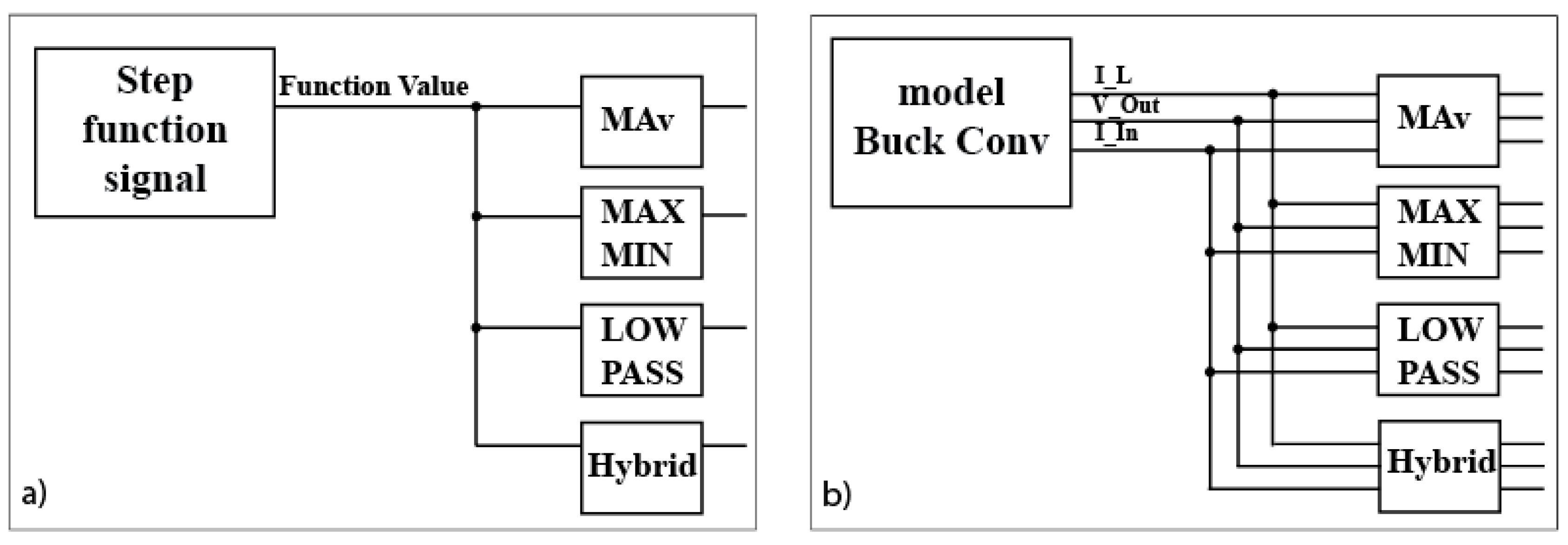
The objective of the paper is to define the most efficient and low-cost algorithm for a filter, the aim of which is obtaining the average value of the input signal. The main difference from other common filters should be its adaptive character. The new filter will represent the average value during each switching period. The switching period can vary from cycle to cycle and is defined by a different signal, which is the input/s to the switch/es (i.e., the gate signals). These control signals (SW in the figures) are auxiliary inputs to the proposed filters, which are binary (on or off).
This paper presents four digital filters applied to generate the output signal of an HIL system. All the proposed filters consider signed signals so they can handle positive and negative numbers. The hardware architecture of these filters is proposed and mapped onto a Xilinx Artix-7 field FPGA with fixed-point representation.
There are four types of filters based on different mathematical approaches proposed in this paper:
2.1. Mathematical Average Filter (MAv)
The approach used in this filter is based on the mathematical operation of summarizing the input signal in a defined interval in the discrete domain (which is equivalent to integration in the continuous domain) and dividing the result by the number of terms in the sum. The mathematical formula of the MAv filter can be represented as:
where x(i) is the value of the input signal in sample i, N is the number of samples in the current switching cycle, and Y(n) is the value of the output signal.
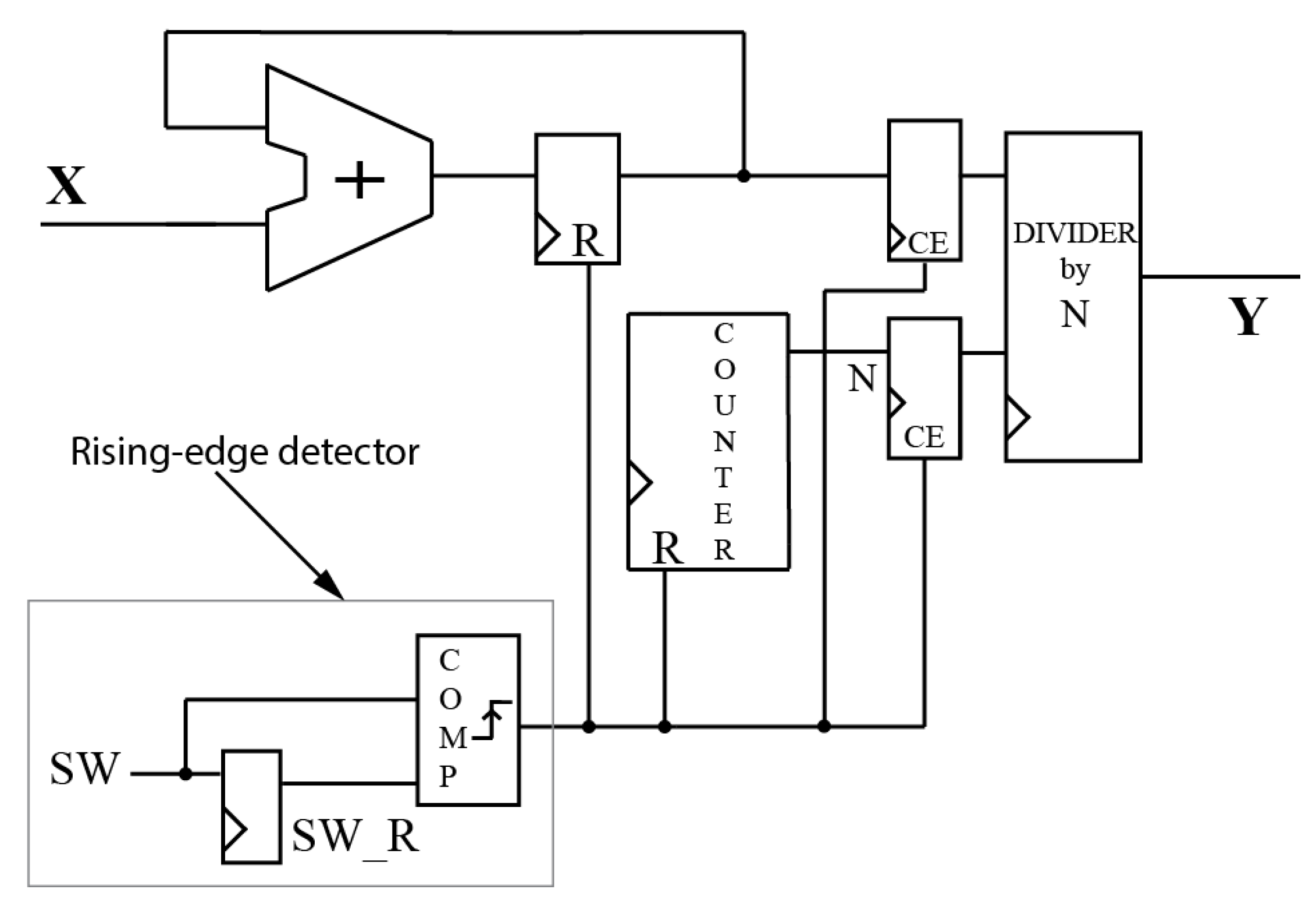
The digital schematic of the Mathematical Average filter is shown in Figure 1. Unfortunately, it is impossible to replace the division with an arithmetic right shift, since shifting can only be used for division by powers of 2, which is not necessarily true in the case of this filtering approach. If N was known a priori, the division could be replaced with a constant (1/N) that is multiplied by the summation. However, an HIL system must be implemented to work with any possible switching frequency without the need for resynthesizing the DAC interface. For this approach, a detector for the rising-edge of the switching signal is used to reset (R input) a counter that measures N, which is used for the division.
In fact, the algorithm represents the definition of the average value in the discrete domain itself. Therefore, the main advantage of this filter is the best level of accuracy which can be obtained and the possibility of applying it to any waveform. However, the only, but significant disadvantage of this method is the need for using a complex hardware operator of division. This causes a decrease in speed and an increase in hardware resources. For that reason, there is a need for an alternative algorithm to reduce the hardware resources while keeping good accuracy.
2.2. Maximum-Minimum Point Filter (MAX-MIN)
The MAX-MIN method is possibly the simplest intuitive approach for obtaining the average value of a signal. The algorithm of this filter is based on detecting the last two extrema of the input signal and calculating the average value of them. The mathematical formula of MAX-MIN filter can be represented as:
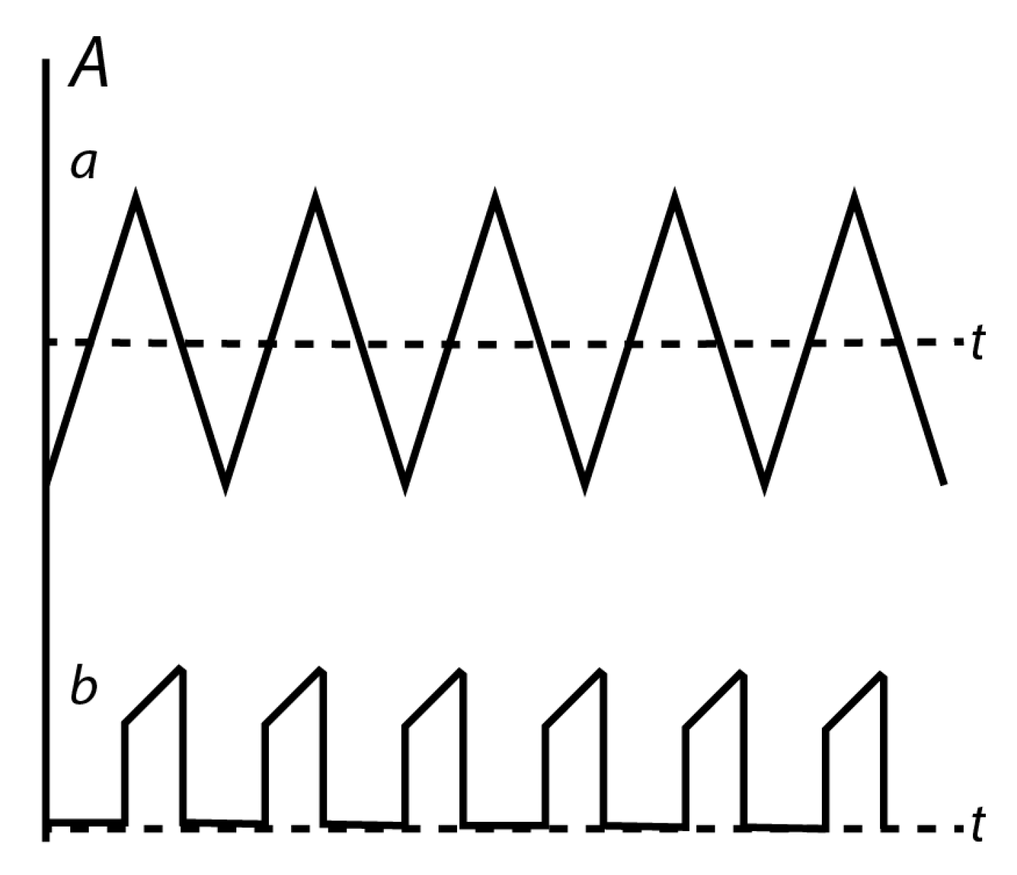
where , are the values of the input signal in the maximum and minimum points in the previous switching period step and is the new value of the output signal. Taking into account that the average value of many typical power waveforms, like the triangular waveform of Figure 2 is the same in both slopes, the output of this filter can be updated twice per switching period. One value represents the average during the on-time and the other represents the average during the off-time. In this way, the latency is reduced to half compared to MAv.
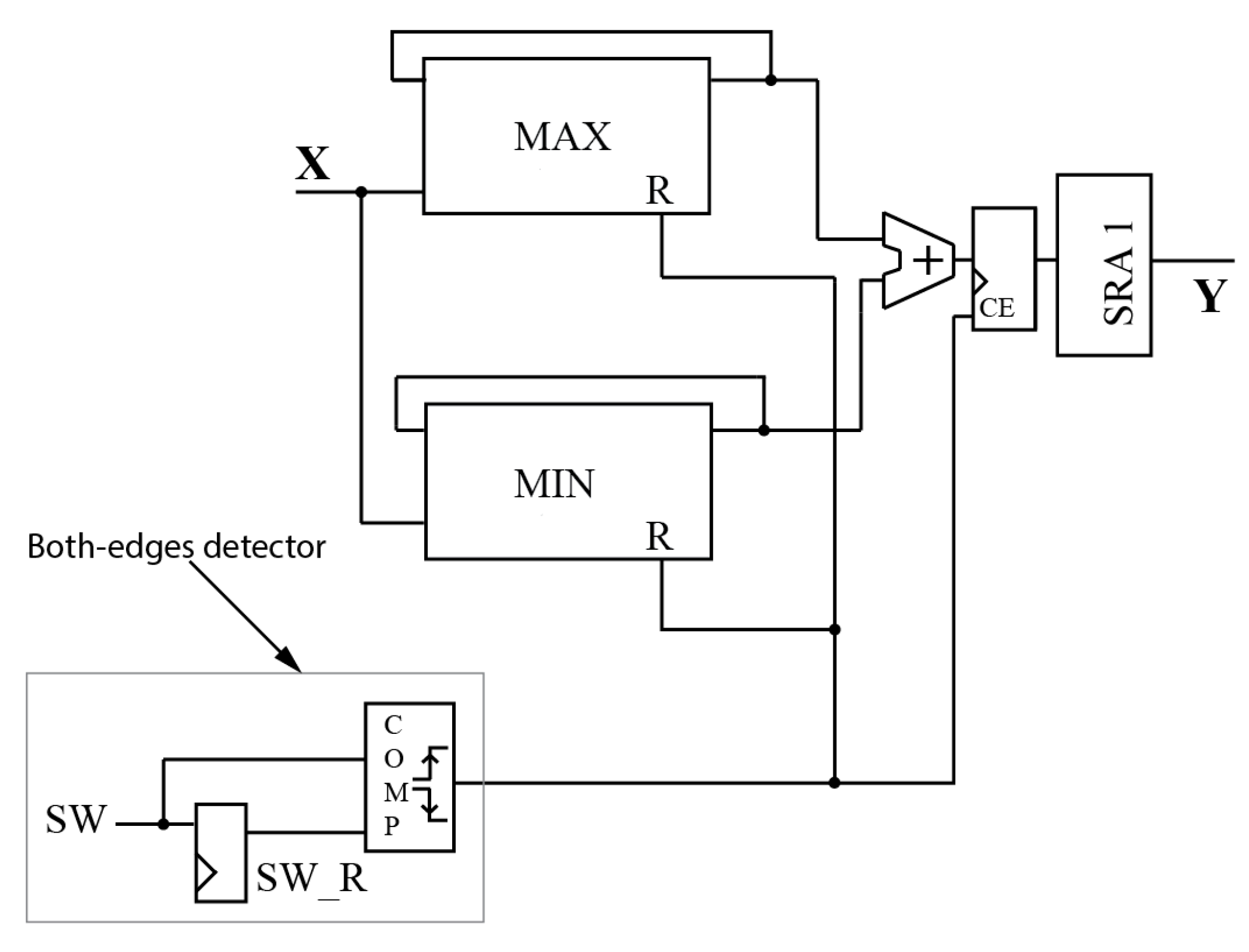
Figure 3 shows the digital schematic of the proposed filtering algorithm. As can be seen from the schematic, a rising-edge detector of the switching signal is used to reset the MAX and MIN blocks (R input) to the opposite side – the lowest value for the MAX block and the highest value for the MIN block. This is used to delete all data from the previous switching period. In addition, there is another switching period event detector which detects both edges to update the filter output. Using both edges to do this allows the system to increase the output frequency. In order to use fewer hardware resources, the operation of division by 2 is made by an arithmetic right shift by 1 (SRA1 in Figure 3), since these two operations are interchangeable in fixed-point notation.
Considering that no division is required to calculate the output, this algorithm obtains a significant efficiency advantage over the previous MAv algorithm. A serious disadvantage of the method is that the filtering operation can be applied only for continuous waveforms. For example, two different types of probable input signals are shown in Figure 2. The wave of the first type (a) can be processed with excellent accuracy using the MAX-MIN algorithm, while the wave of the second type (b), which is discontinuous, cannot be filtered correctly using this method. Hence, the second algorithm can be used in continuous waveforms in which the average is equal to Equation (2).
2.3. Low-Pass and Hybrid Low-Pass Filters (LOW-PASS, Hybrid)
The third and the fourth filters are an infinite impulse response filter (IIR), specifically, a non-delay version of first-order low-pass filters with gain [34]. The transfer function of the filters can be expressed as Equation (3) and its finite difference equation in Equation (4).
where is a constant coefficient value, which depends on the cut-off frequency (5). The cut-off frequency should be chosen depending on the desired attenuation:
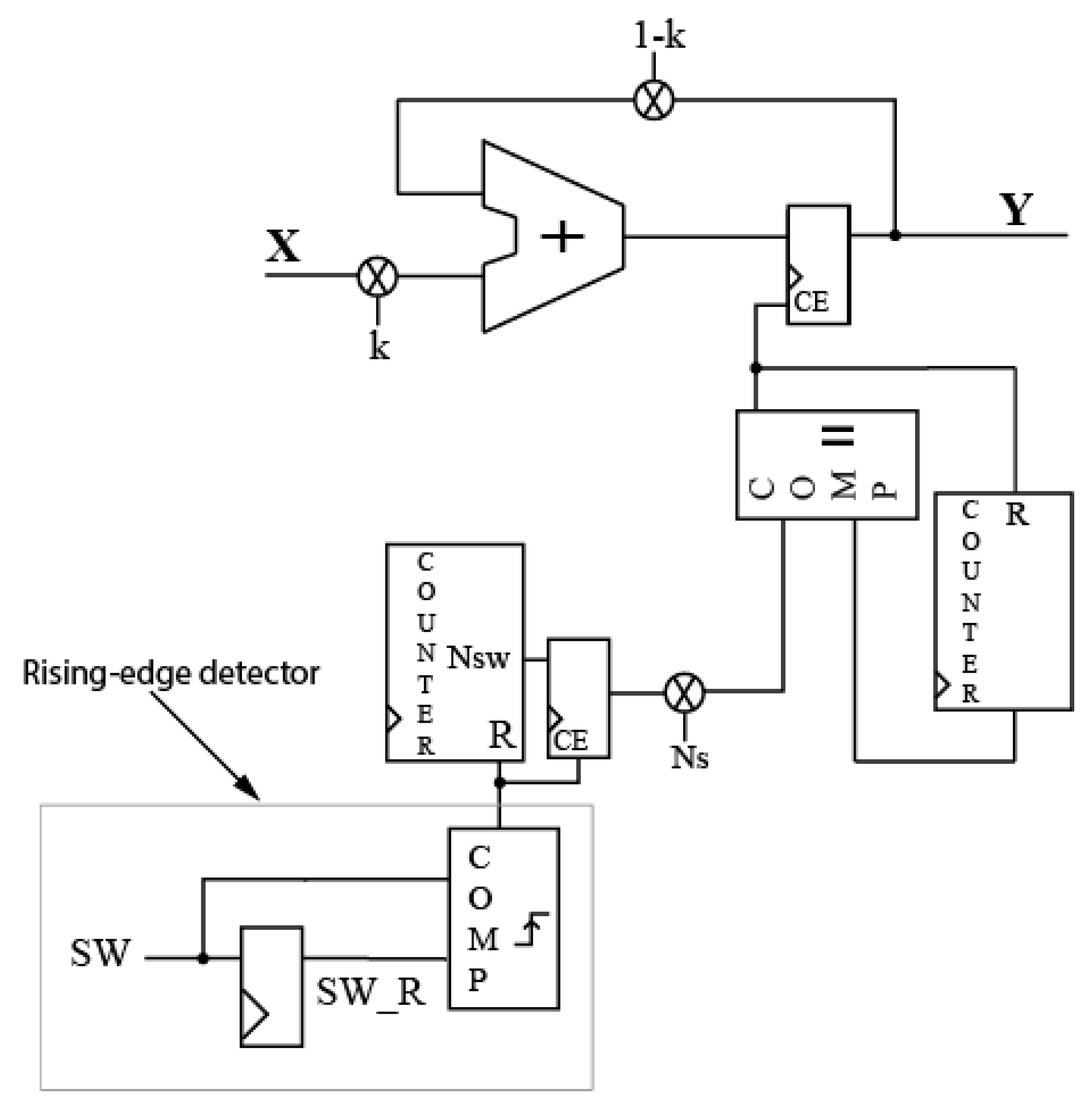
where is the desired attenuation, is the switching frequency, is the filter sampling frequency, and is the clock frequency. The filters have been designed in order to obtain 128 samples per switching period as can be seen in Equation (6). The number 128—power of two—was chosen with the aim of optimizing the filter, using arithmetic right shifting instead of dividing, as for the second filter. This can be seen from the digital schematic in Figure 4.
The maximum of the sampling frequency is equal to the clock frequency of , therefore the filter can be applied only to frequencies, which correspond to the condition Equation (7). The sampling frequency is being adapted proportionally to the switching frequency, which consequently causes the change of cut-off frequency without changing the constant . Therefore, the adaptive algorithm of the LOW-PASS filter provides the same level of attenuation for all the possible switching frequencies. To do that, the left counter of Figure 4 obtains the number of clock cycles in a switching period (Nsw). When the switching period has finished—using the rising-edge detector of the switching cycle—that number is multiplied by Ns. Ns is a constant defined as , so the system always takes 128 samples per switching cycle.
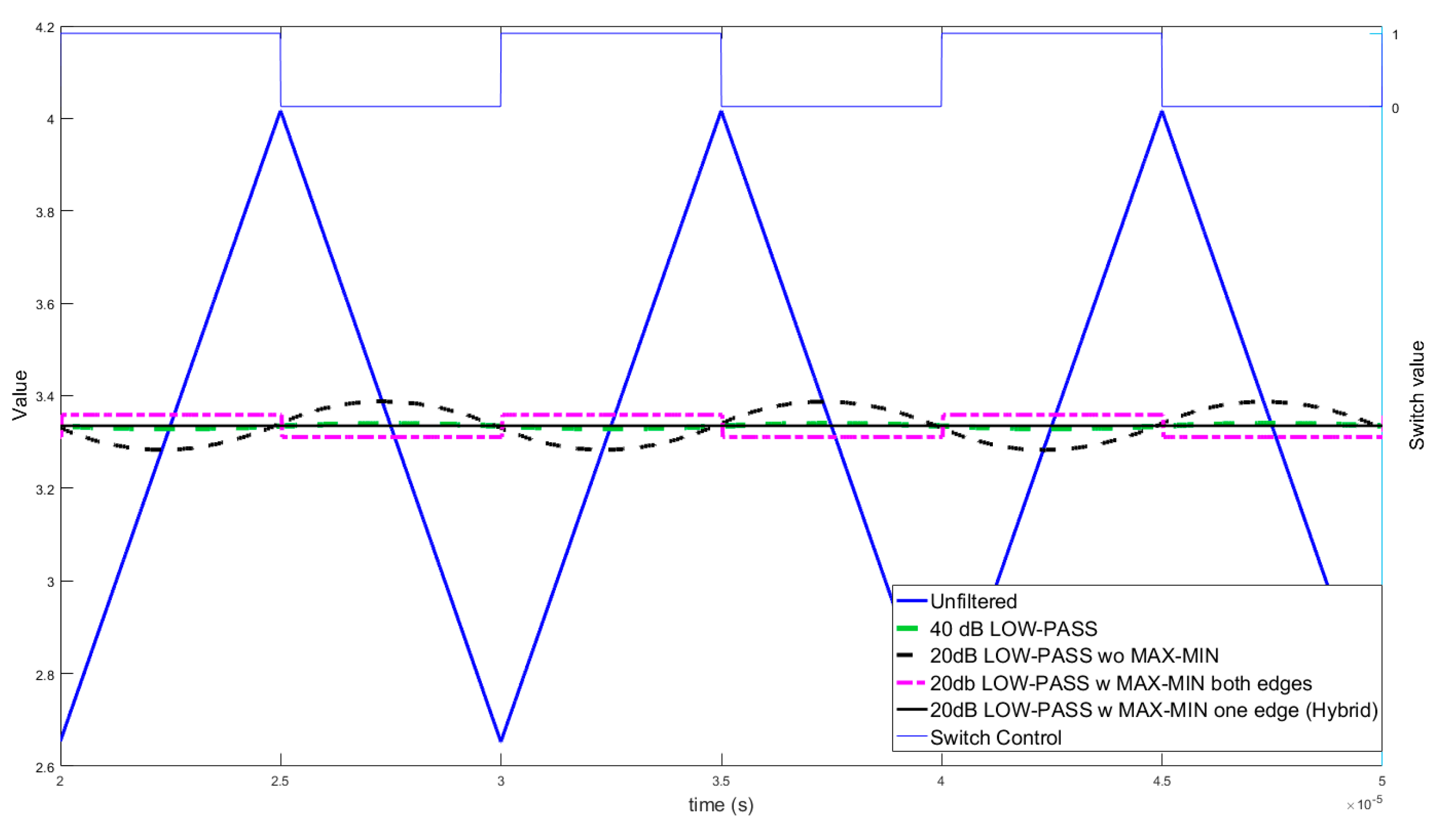
The choice of the attenuation is not trivial. The aim of the filter is to reduce the ripple of the values generated by the HIL model, so higher attenuations will provide better accuracy, i.e., an output signal without switching ripple. However, the increase in attenuation leads to a proportional increase in the delay of the filter output. Figure 5 shows an example of a triangular wave, a 40 dB filter output with a negligible ripple and a 20 dB filter output with a significant ripple. Regarding accuracy, the 40 dB filter is clearly better. However, the delay is proportional to the attenuation, as it will be shown in Figure 8. Therefore, in order to have better accuracy, higher attenuation leads to a higher delay.
A trade-off situation between delay and accuracy should be reached. A lower attenuating filter, which is faster, can be used and its output can be driven to an additional MAX-MIN filter. Figure 5 also shows the output of the 20 dB filter combined with MAX-MIN in two cases. The original MAX-MIN filter updates on both edges of the switch control signal. This is not appropriate for the output of the LOW-PASS filter because its average is different during the on and off time, and two average values are obtained. The solution is to update the MAX-MIN filter only once per switching period, thereby obtaining the real average per switching cycle. Figure 6 shows the schematic of the proposed Hybrid architecture that combines a low pass filter with the MAX-MIN algorithm applied only in the rising-edge of the switching signal.
3. Results
In this section, a comparison of the four proposed filters is presented. In order to demonstrate the difference between the effect of algorithms, several simulations and implementations were made (see Figure 7). The first one is the direct simulation of the filters with a step-function input to check their dynamics in a simple test. The second experiment is the integration of the proposed filters with a real-time HIL model of an asynchronous buck converter so the dynamics of the full system are shown. Finally, this section presents a comparison of the impact on the area and minimum achievable period clock. Design tools such as ModelSim and Vivado, respectively, were used for this aim.
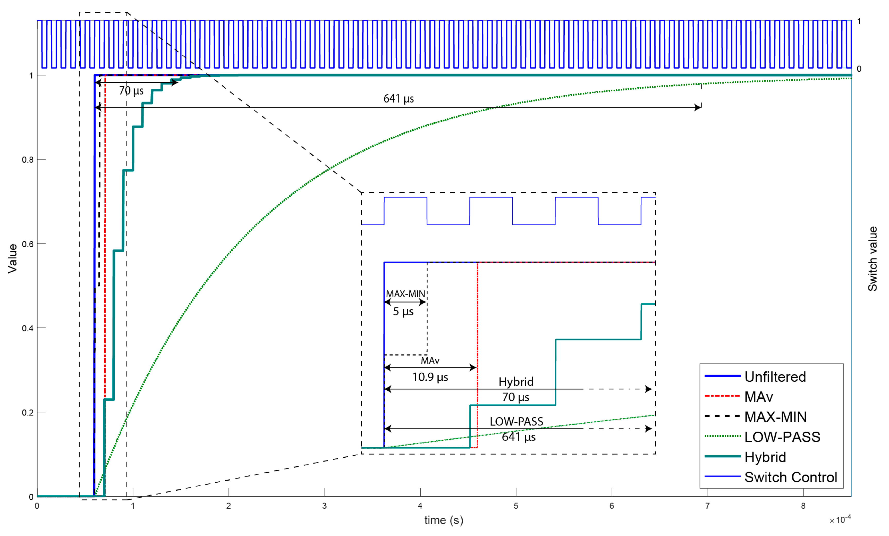
The first simulation experiment was carried out by connecting a step function signal to the input of the filters, as shown in Figure 7a. This experiment was made with the aim of proving the theoretical working principles of the proposed algorithms. Figure 8 proves that the experimental results of all MAv, MAX-MIN, LOW-PASS, and Hybrid filters meet the theoretical expectations. It can be seen that the MAv filter is being applied to each rising edge of the control signal with a small delay, caused by the delay of the hardware and medium algorithm complexity. The MAX-MIN filter is being updated during every event of the control signal, which can be also observed in Figure 8. In the first event of the control signal after the input is 1, the MAX-MIN filter gives an output of 50%, because it considers the current value (1) and the previous value (0). In the next control signal event, the output gets the final value, which is 100%. As can be seen, the MAX-MIN filter has the smallest, almost unnoticeable, latency time among the proposed filters, according to its simplest algorithm. In contrast with the MAX-MIN filter, the 40 dB LOW-PASS filter shows the slowest dynamic, caused mainly by the delay of the algorithm, while the Hybrid filter which uses an attenuation of 20 dB is about 10 times faster but still slower than the MAv and the MAX-MIN. To conclude the results of the step signal filtering, it must be said that all the proposed filters obtain the correct result after the corresponding latencies, so the mathematical approaches for these filters were chosen correctly.
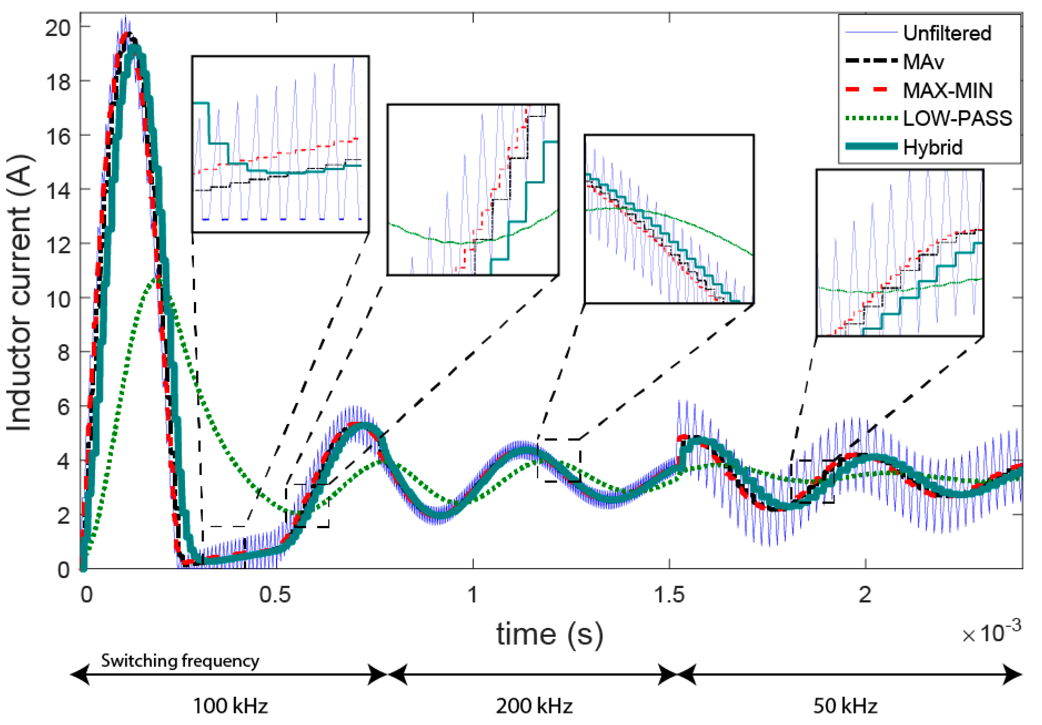
The second simulation experiment was done by connecting the inputs of the filters to the outputs of a real-time HDL model of an asynchronous buck converter as can be seen in Figure 7b. The outputs of the HIL model are inductor current (I_L), output voltage (V_Out) and input current (I_In). The implementation of the buck converter model is described in reference [30]. The selected physical buck converter parameters used for experimental results are presented in Table 1.
Figure 9 shows a transition from power off to nominal operation using a constant duty cycle. The accuracy of the LOW-PASS filter is significantly worse than the accuracy of MAv and MAX-MIN filters because of its slow dynamic. Considering this, the following experimental conclusion can be made: the 40 dB LOW-PASS filter is not applicable for use during transients. However, the hybrid filter shows better dynamics. We have to take into account that the switching frequency is not constant in many applications. Therefore, during the experiment made for Figure 9, the switching frequency has been changed from the original one, 100 kHz, to 200 kHz and 50 kHz in order to test the behavior. The experiment shows that the proposed filters are updated correctly for the different frequency ranges. It is also noticeable that if the switching frequency is lower, and therefore closer to the natural frequencies of the power converter, the relative importance of latency increases. For example, when the switching frequency is 50 kHz (right part of Figure 9) the phase delay of the Hybrid filter is clearly visible. However, when the switching frequency is 200 kHz, the phase delay is much smaller. The results of the output voltage and input current have the same behavior, so they are not shown in this paper for the sake of shortness.
It is also important to notice that during discontinuous mode (between 0.25 and 0.5 ms) the MAX-MIN filter cannot lead to proper results because the average of the extrema is not the real average of the current. As can be seen in the first zoomed figure, the current filtered by the MAX-MIN method has a significant deviation, as was predicted in Section 2.2. In this case, this filter output higher is above the real average. However, during the rest of the time this filter gives accurate results, since the current is in continuous mode.
Finally, the proposed filters were implemented and tested on a Xilinx FPGA Artix-7 chip XC7A35TICSG324-1L using the design tool Vivado 2018.3. Table 2 presents the synthesis results of the emulation systems after the implementation. The table shows the results in area and speed. Two different syntheses were carried out. 1) The HIL system from the second experiment, which includes the buck converter and different filtering architectures, one for each output signal (I_L, V_Out, I_In). 2) Only one filter did not have any model connected to it, to check the hardware resources needed for all the proposed methods so they can be compared to the resources used for the power converter model.
All the systems have been also synthesized without using DSP blocks to perform a fair comparison of the logic usage. Of course, in a real application, this is not recommended because the minimum period can become significantly higher. According to the table, the MAv filter needs much more hardware resources than the other three filters. The reason for this is that the fixed-point divider, used in the mathematical average filter, is a complex operation that requires a large number of resources. For example, most part of the LUTs needed for the MAv filter without the model, specifically 778 out of 798, were used for the division. The smallest quantity of hardware resources is taken for the MAX-MIN filter because of its simplicity. And the LOW-PASS filters require more resources than the simplest MAX-MIN, but still need much less than the MAv. Regarding synthesis time results, the table II shows that the maximum frequency that can be obtained for the MAX-MIN filter is 1.16 times higher than the MAv, around 2.79 times higher than the LOW-PASS, and 2.84 times higher than the LOW-PASS hybrid. However, it must be underlined that in the current situation area, resources of the filters play a much more important role than the time resources. In the end, the minimum period of a complete system is defined by the speed of the model, not the filters (as it can be also seen in Table 2).
Table 2 also shows the CPI (Cost Performance Index) of all the proposed methods. The CPI has been defined following the formula:
The latency number is the one obtained in the experiment shown in Figure 8. In the case of the low-pass filters, their settling times (98%) have been used. This index has been applied only for the non-DSP versions so they can be compared fairly in terms of area (LUTs). For the CPI, latency has been chosen instead of the minimum clock period because the filter latency is the most important factor for the user. In the previous formula, filters with higher values have a better trade-off between dynamics and area usage. The latency would change with the switching frequency because all the filters are executed with that reference. As the latency will grow proportional to the switching cycle in all cases, the CPI ratio between filters will remain basically the same.
From all the above, a proper filtering approach must be chosen depending on the input waveform. The MAX-MIN filter shows significantly better CPI than the other three filters because it is the fastest and simplest filter. Therefore, if the type of waveform allows proper filtering via the MAX-MIN (continuous waveform), it is highly recommended to use it. On the other hand, the 40 dB low-pass filter should be discarded because it has no clear advantage compared with the hybrid architecture: it has a much higher latency and similar area.
If the type of waveform is not suitable for the MAX-MIN method, the MAv and Hybrid methods should be considered. MAv approach has better CPI and therefore better global performance. But in each application, the relative importance of latency and area should be considered. If latency is very important—e.g., if the switching frequency is relatively low—MAv should be chosen. However, if the area is more important than the latency, the Hybrid filter may be a good choice.
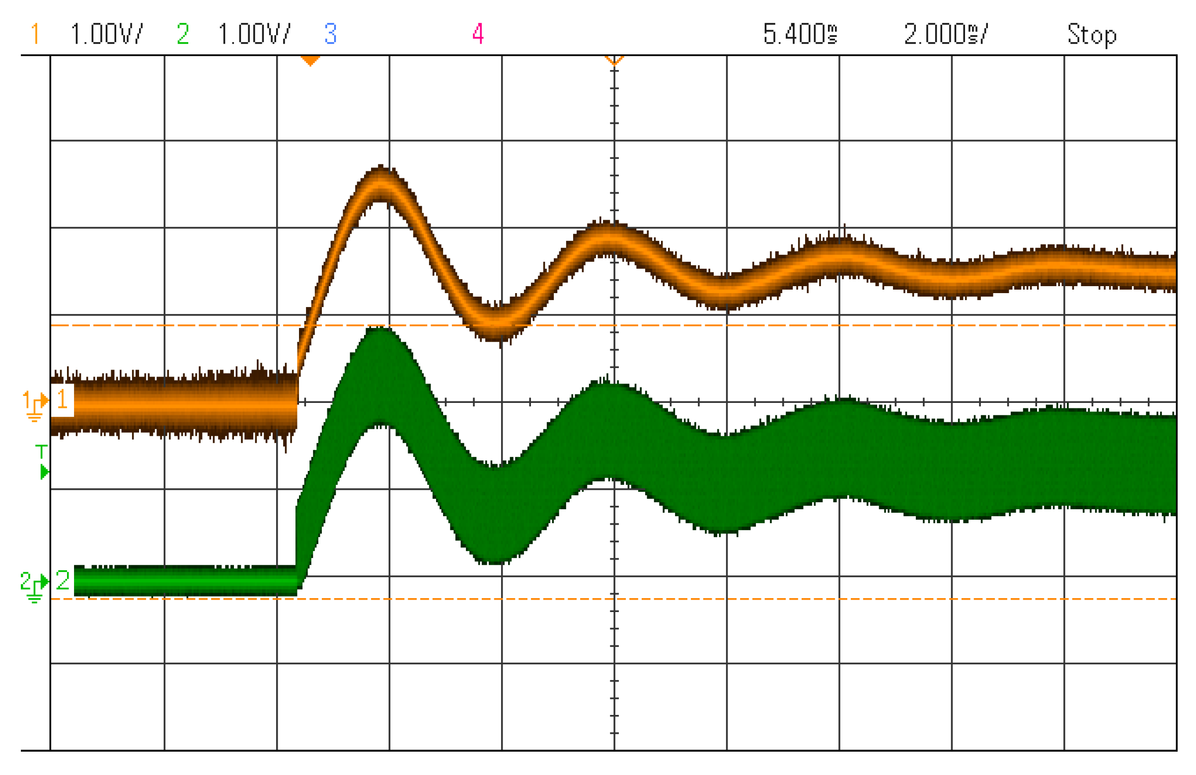
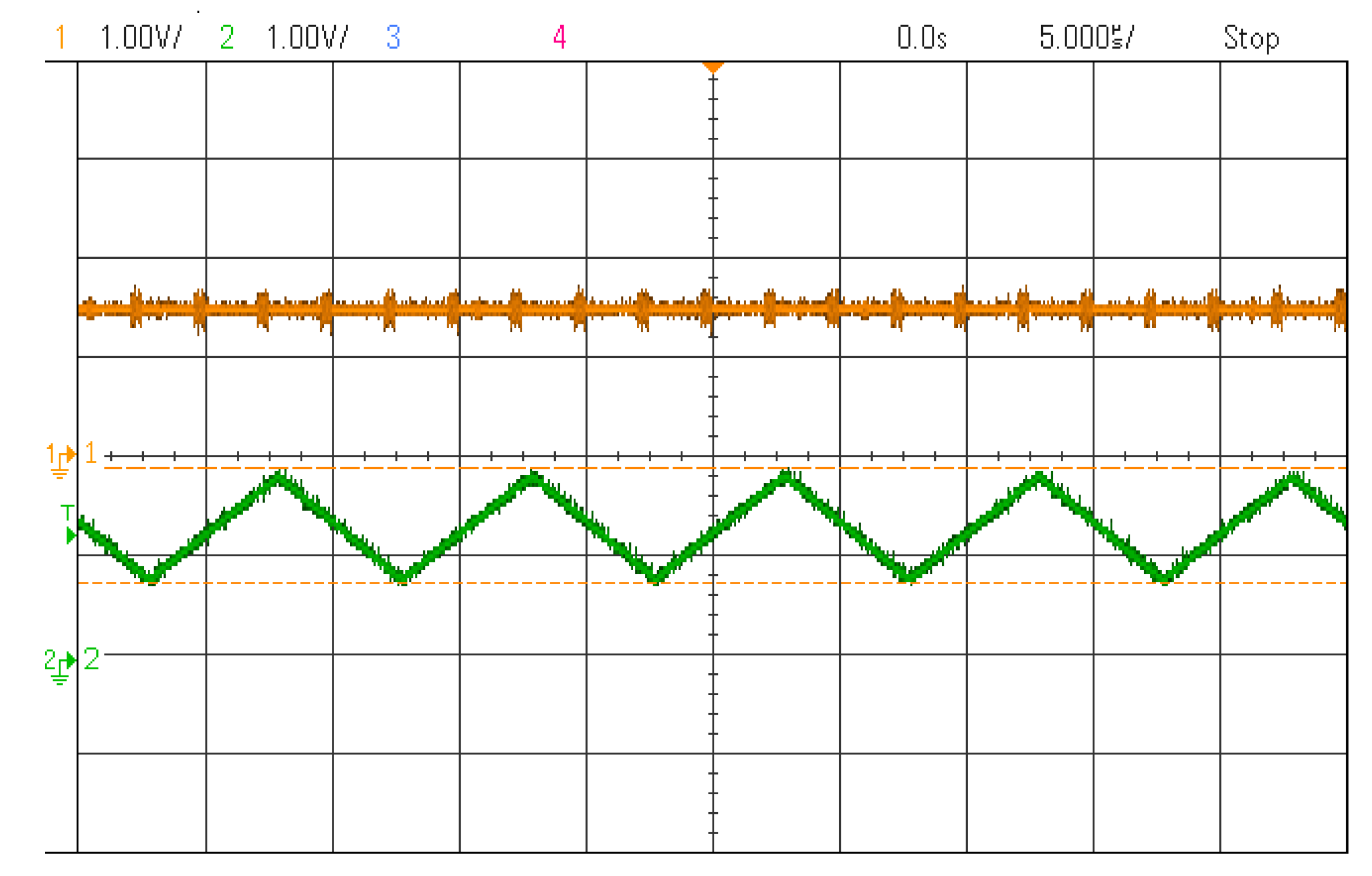
Finally, all the models have been downloaded to a Digilent Arty A7-35 to check the integration of the complete HIL system (model and DACs). Figure 10 shows the transient process of the inductor current of a buck converter with two different DACs: a high-speed DAC (AD9767 from Analog Devices)—lower line—and a low-speed DAC (PMOD DA2 from Digilent)—higher line. The output that goes to the low-speed DAC has been previously filtered using the MAX-MIN filter. Therefore, the ripple has been removed while having the same numerical average results. Likewise, Figure 11 shows the steady-state of both DACs. It is obvious that a high-speed DAC offers a more realistic analog output but, as was explained in Section 1, high-speed DACs have parallel interfaces so they require a lot of FPGA output pins to be used. As the number of output analog channels of a HIL system is growing in importance and the overall cost of HIL platforms is decreasing, the use of cheaper and lower pin count DACs must be taken into account. As these DACs offer lower speed, using the proposed filters may be considered as an alternative.
4. Conclusions
This paper presents a comparison between four different filtering methods to interface low-speed DACs in HIL applications. The filters were designed to be implemented in FPGAs and experimentally applied to the most common types of waveforms (triangular and non-triangular types) of switched power converters. MAX-MIN is based on taking two samples every half-cycle and getting their average. The MAv method gets the average of as many samples as can be taken at the system clock frequency. 40 dB LOW-PASS implements a classic first-order low-pass filter with high attenuation. Finally, a Hybrid architecture merges a 20 dB low-pass filter with the MAX-MIN method, getting more ripple after the classic low-pass filter but removing it with MAX-MIN.
The first conclusion is that the MAX-MIN method is the simplest and fastest filter (15% faster than MAv, 275% faster than 40 dB LOW-PASS, and 320% faster than Hybrid), but it cannot be applied for discontinuous waveforms. In that case, another method is necessary.
Results show that MAv is the method with the lowest latency that can be applied to any waveform. However, it requires the largest area (135% more LUTs than 40 dB LOW-PASS, and 93% more than Hybrid). LOW-PASS filters significantly decrease the area at the expense of the latency. Latency can be decreased reducing the attenuation of the filter, but the switching ripple would increase, going against the objective of these filters. A trade-off can be reached using a hybrid architecture composed by a low-attenuation LOW-PASS filter followed by a MAX-MIN filter.
Finally, from the methods which can be applied to any waveform, MAv has the best global performance measured by CPI (25 times better than 40 dB LOW-PASS, and 3.3 times better than Hybrid), but the final decision should be taken while considering the relative importance of the latency and area. When latency is the key factor, MAv is the best choice, while a hybrid filter is the best option for the area.
Author Contributions
Conceptualization, M.Y., A.S. and A.d.C.; methodology, M.Y. and A.d.C.; software, M.Y. and A.S.; validation, M.Y., A.S., A.d.C. and M.S.M.-G.; writing—original draft preparation, M.Y. and A.S.; writing—review and editing, M.Y., A.S. and M.S.M.-G.; and Supervision, A.d.C.
Funding
This research was funded by Spanish Ministerio de Economía y Competitividad grant number TEC2013-43017-R.
Conflicts of Interest
The authors declare no conflict of interest.
References
- Patella, B.; Prodic, A.; Zirger, A.; Maksimovic, D. High-frequency digital PWM controller IC for DC-DC converters. IEEE Trans. Power Electron. 2003, 18, 438–446. [Google Scholar] [CrossRef]
- An, F.; Song, W.; Yang, K. Direct power control of dual-active-bridge DC-DC converters based on unified phase shift control. J. Eng. 2019, 16, 2180–2184. [Google Scholar] [CrossRef]
- Buso, S.; Malesani, L.; Mattavelli, P. Comparison of current control techniques for active filter applications. IEEE Trans. Ind. Electron. 1998, 45, 722–729. [Google Scholar] [CrossRef]
- Van de Sype, D.M.; Gusseme, K.D.; Van den Bossche, A.P.M.; Melkebeek, J.A. Duty-ratio feedforward for digitally controlled boost PFC converters. IEEE Trans. Ind. Electron. 2015, 52, 108–115. [Google Scholar] [CrossRef]
- Salehifar, M.; Moreno-Eguilaz, M.; Putrus, G.; Barras, P. Simplified fault-tolerant finite control set model predictive control of a five-phase inverter supplying BLDC motor in electric vehicle drive. Electr. Power Syst. Res. 2016, 132, 56–66. [Google Scholar] [CrossRef]
- Tir, Z.; Malik, O.P.; Eltamaly, A.M. Fuzzy logic based speed control of indirect field oriented controlled double star induction motors connected in parallel to a single six-phase inverter supply. Electr. Power Syst. Res. 2016, 134, 126–133. [Google Scholar] [CrossRef]
- Wang, M.; Xu, L.; Wang, K.; Zheng, Z.; Li, Y.; Grada, C.; Zhang, H. Hardware-in-the-loop real-time platform for more electric aircraft. J. Eng. 2018, 2018, 446–452. [Google Scholar] [CrossRef]
- Abdelrahman, A.S.; Algarny, K.S.; Youssef, M.Z. A Novel Platform for Powertrain Modeling of Electric Cars with Experimental Validation Using Real-Time Hardware in the Loop (HIL): A Case Study of GM Second Generation Chevrolet Volt. IEEE Trans. Power Electron. 2018, 33, 9762–9771. [Google Scholar] [CrossRef]
- Tong, Z.; Zhang, H.; Ye, Z.; Han, J. RCP-based HIL Simulation and Control for 2-DOF Tracking Robot of Maneuvering. In Proceedings of the 2009 International Asia Conference on Informatics in Control; Automation and Robotics (CAR), Bangkok, Thailand, 1–2 February 2009; pp. 121–125. [Google Scholar] [CrossRef]
- Aiello, G.; Cacciato, M.; Scarcella, G.; Scelba, G. Failure analysis of AC motor drives via FPGA-based hardware-in-the-loop simulations. Electr. Eng. 2017, 99, 1337–1347. [Google Scholar] [CrossRef]
- Chilipi, R.S.R.; Sayari, N.A.; Hosani, K.A.; Beig, A.R. Adaptive notch filter based multipurpose control scheme for grid-interfaced three-phase four-wire DG inverter. In Proceedings of the 2016 IEEE Industry Applications Society Annual Meeting, Portland, OR, USA, 4–6 October 2016; pp. 1–8. [Google Scholar] [CrossRef]
- Vijay, A.S.; Doolla, S.; Chandorkar, M.C. Real-Time Testing Approaches for Microgrids. IEEE J. Emerg. Sel. Top. Power Electron. 2017, 5, 1356–1376. [Google Scholar] [CrossRef]
- Barreras, J.V.; Fleischer, C.; Christensen, A.E.; Swierczynski, M.; Schaltz, E.; Andreasen, S.J.; Sauer, D.U. An Advanced HIL Simulation Battery Model for Battery Management System Testing. IEEE Trans. Ind. Appl. 2010, 52, 5086–5099. [Google Scholar] [CrossRef]
- Sparn, B.; Krishnamurthy, D.; Pratt, A.; Ruth, M.; Wu, H. Hardware-in-the-Loop (HIL) Simulations for Smart Grid Impact Studies. In Proceedings of the 2018 IEEE Power & Energy Society General Meeting (PESGM), Portland, OR, USA, 5–9 August 2018; pp. 1–5. [Google Scholar] [CrossRef]
- Corpino, S.; Stesina, F. Verification of a CubeSat via hardware-in-the-loop simulation. IEEE Trans. Aerosp. Electron. Syst. 2014, 50, 2807–2818. [Google Scholar] [CrossRef]
- Luo, Y.; Li, Z.; Xu, L.; Xiong, X.; Li, Y.; Zhao, C. An Adaptive Voltage-Balancing Method for High-Power Modular Multilevel Converters. IEEE Trans. Power Electron. 2018, 33, 2901–2912. [Google Scholar] [CrossRef]
- Said, S.B.; Saad, K.B.; Benrejeb, M. HIL simulation approach for a multicellular converter controlled by sliding mode. Int. J. Hydrog. Energy 2017, 42, 12790–12796. [Google Scholar] [CrossRef]
- Sandre-Hernandez, O.; Rangel-Magdaleno, J.; Morales-Caporal, R.; Bonilla-Huerta, E. HIL simulation of the DTC for a three-level inverter fed a PMSM with neutral-point balancing control based on FPGA. Electr. Eng. 2018, 100, 1441–1454. [Google Scholar] [CrossRef]
- Grégoire, L.; Al-Haddad, K.; Nanjundaiah, G. Hardware-in-the-Loop (HIL) to reduce the development cost of power electronic converters. In Proceedings of the 2011 India International Conference on Power Electronics, New Delhi, India, 28–30 January 2011; pp. 1–6. [Google Scholar] [CrossRef]
- Ji, F.; Fan, H.; Sun, Y. Modelling a FPGA-based LLC converter for real-time hardware-in-the-loop (HIL) simulation. In Proceedings of the 2016 IEEE 8th International Power Electronics and Motion Control Conference (IPEMC-ECCE Asia), Hefei, China, 22–26 May 2016; pp. 1016–1019. [Google Scholar] [CrossRef]
- Li, W.; Jean, B. An equivalent circuit method for modelling and simulation of modular multilevel converter in real-time HIL test bench. In Proceedings of the 2017 IEEE Power & Energy Society General Meeting, Chicago, IL, USA, 16–20 July 2017; p. 1. [Google Scholar] [CrossRef]
- Sanchez, A.; Todorovich, E.; De Castro, A. Exploring the Limits of Floating-Point Resolution for Hardware-In-the-Loop Implemented with FPGAs. Electronics 2018, 7, 219. [Google Scholar] [CrossRef]
- Rosa, A.H.R.; Silva, M.B.E.; Campos, M.F.C.; Santana, R.A.S.; Rodrigues, W.A.; Morais, L.M.F.; Seleme, I.S., Jr. SHIL and DHIL Simulations of Nonlinear Control Methods Applied for Power Converters Using Embedded Systems. Electronics 2018, 7, 241. [Google Scholar] [CrossRef]
- Kokenyesi, T.; Durbák, N.; Varjasi, I. FPGA-synthesizable filter model based bitstream DAC for hardware-in-the-loop simulators. In Proceedings of the 21st IMEKO TC-4 International Symposium and 19th International Workshop on ADC Modelling and Testing, Budapest, Hungary, 7–9 September 2016; pp. 202–207. [Google Scholar]
- Kokenyesi, T.; Hegedus, M.; Vereb, S.; Balogh, A.; Suto, Z.; Varjasi, I. FPGA-Driven DAC with Second Order Sliding Mode Control of Filter Model for Hardware-In-the-Loop Simulators. In Proceedings of the 2018 IEEE 18th International Power Electronics and Motion Control Conference (PEMC), Budapest, Hungary, 26–30 August 2018; pp. 824–829. [Google Scholar] [CrossRef]
- Typhoon HIL. Available online: https://www.typhoon-hil.com (accessed on 11 December 2017).
- dSPACE. Available online: https://www.dspace.com (accessed on 11 December 2017).
- OPAL-RT. Available online: https://www.opal-rt.com (accessed on 11 December 2017).
- Fernández-Álvarez, A.; Portela-García, M.; García-Valderas, M.; López, J.; Sanz, M. HW/SW Co-Simulation System for Enhancing Hardware-in-the-Loop of Power Converter Digital Controllers. IEEE J. Emerg. Sel. Top. Power Electron. 2017, 5, 1779–1786. [Google Scholar] [CrossRef]
- Sanchez, A.; de Castro, A.; Garrido, J. Parametrizable fixed-point arithmetic for HIL with small simulation steps. IEEE J. Emerg. Sel. Top. Power Electron. 2018, 1, 1–9. [Google Scholar] [CrossRef]
- Sanchez, A.; de Castro, A.; Garrido, J. A Comparison of Simulation and Hardware-in-the-Loop Alternatives for Digital Control of Power Converters. Ieee Trans. Ind. Inform. 2012, 8, 491–500. [Google Scholar] [CrossRef]
- Rodríguez, M.; Zhang, Y.; Maksimović, D. High-Frequency PWM Buck Converters Using GaN-on-SiC HEMTs. IEEE Trans. Power Electron. 2014, 29, 2462–2473. [Google Scholar] [CrossRef]
- Kassakian, J.G.; Jahns, T.M. Evolving and Emerging Applications of Power Electronics in Systems. IEEE J. Emerg. Sel. Top. Power Electron. 2013, 1, 47–58. [Google Scholar] [CrossRef]
- Oppenheim, A.V.; Schafer, R.W.; Buck, J.R. Discrete-Time Signal Processing, 2nd ed.; Prentice-Hall: Upper Saddle River, NJ, USA, 1999. [Google Scholar]
Figure 1.
Digital schematic of the mathematical average (Mav) filter.

Figure 2.
Some possible types of the waveform.

Figure 3.
Digital schematic of the maximum-minimum point (MAX-MIN) filter.

Figure 4.
Digital schematic of the LOW-PASS filter.

Figure 5.
Comparison of the low pass and hybrid filter.

Figure 6.
Digital schematic of the Hybrid filter.

Figure 7.
Architecture of the experiments shown in this section. (a) Model of the step function signal connected to the filters. (b) Model of the buck converter, connected to the filters.
Figure 7.
Architecture of the experiments shown in this section. (a) Model of the step function signal connected to the filters. (b) Model of the buck converter, connected to the filters.

Figure 8.
Comparison of the filters, applied to the step function signal.

Figure 9.
Comparison of the filters applied to the inductor current of a buck converter model.

Figure 10.
Comparison between a high-speed (lower wave) and low-speed (higher wave) DACs (Digital-to-Analog Converters). The transient process of a buck converter following the architecture of Figure 7b.
Figure 10.
Comparison between a high-speed (lower wave) and low-speed (higher wave) DACs (Digital-to-Analog Converters). The transient process of a buck converter following the architecture of Figure 7b.

Figure 11.
Comparison between a high-speed (lower wave) and low-speed (higher wave) DACs. The steady-state of a buck converter following the architecture of Figure 7b.
Figure 11.
Comparison between a high-speed (lower wave) and low-speed (higher wave) DACs. The steady-state of a buck converter following the architecture of Figure 7b.


Table 1.
Buck Converter Parameters.
| Parameter | Value |
|---|---|
Table 2.
Comparison of used field programmable gate array (FPGA) resources.
| System | HIL Model + 3 Filters | Without Model (1 Filter) | Overall Results | |||||||
|---|---|---|---|---|---|---|---|---|---|---|
| Min Period (ns) | terms of area (LUTs) | FFs | Digital Signal Processors (DSPs) 25 × 18 | Min Period (ns) | LUTs | FFs | DSPs 25 × 18 | Latency (μs) | ||
| MAv | 15.692 | 2739 | 7502 | 2 | 3.271 | 798 | 2467 | 0 | - | - |
| MAv(no DSPs) | 15.785 | 2828 | 7501 | 0 | - | - | - | - | 10.9 | 114.9 |
| MAX-MIN | 15.023 | 450 | 260 | 2 | 2.825 | 38 | 53 | 0 | - | - |
| MAX-MIN (no DSPs) | 15.331 | 560 | 259 | 0 | - | - | - | - | 5 | 5263.2 |
| 40 dB LOW-PASS | 17.822 | 720 | 423 | 14 | 9.116 | 122 | 91 | 4 | - | - |
| 40 dB LOW-PASS (no DSPs) | 16.995 | 1495 | 339 | 0 | 10.589 | 339 | 78 | 0 | 641 | 4.6 |
| Hybrid (20dB + MAX-MIN) | 16.302 | 857 | 605 | 14 | 9.299 | 191 | 133 | 4 | - | - |
| Hybrid (20dB + MAX-MIN) (no DSPs) | 17.713 | 1687 | 502 | 0 | 11.850 | 414 | 133 | 0 | 70 | 34.5 |
© 2019 by the authors. Licensee MDPI, Basel, Switzerland. This article is an open access article distributed under the terms and conditions of the Creative Commons Attribution (CC BY) license (http://creativecommons.org/licenses/by/4.0/).
Share and Cite
MDPI and ACS Style
Yushkova, M.; Sanchez, A.; de Castro, A.; Martínez-García, M.S. A Comparison of Filtering Approaches Using Low-Speed DACs for Hardware-in-the-Loop Implemented in FPGAs. Electronics 2019, 8, 1116. https://doi.org/10.3390/electronics8101116
AMA Style
Yushkova M, Sanchez A, de Castro A, Martínez-García MS. A Comparison of Filtering Approaches Using Low-Speed DACs for Hardware-in-the-Loop Implemented in FPGAs. Electronics. 2019; 8(10):1116. https://doi.org/10.3390/electronics8101116
Chicago/Turabian StyleYushkova, Marina, Alberto Sanchez, Angel de Castro, and M. Sofía Martínez-García. 2019. "A Comparison of Filtering Approaches Using Low-Speed DACs for Hardware-in-the-Loop Implemented in FPGAs" Electronics 8, no. 10: 1116. https://doi.org/10.3390/electronics8101116
Note that from the first issue of 2016, this journal uses article numbers instead of page numbers. See further details here.