Article

Improvement of Stability in a PCM-Controlled Boost Converter with the Target Period Orbit-Tracking Method

1
School of Electric Power, South China University of Technology, Guangzhou 510641, China
2
School of Automation, Guangdong University of Technology, Guangzhou 510640, China
*
Author to whom correspondence should be addressed.
Electronics 2019, 8(12), 1432; https://doi.org/10.3390/electronics8121432
Submission received: 24 October 2019 / Revised: 23 November 2019 / Accepted: 27 November 2019 / Published: 30 November 2019
(This article belongs to the Special Issue Power Converters in Power Electronics)

Abstract

:
Thee peak-current-mode (PCM) control strategy is widely adopted in pulse width-modulated (PWM) DC-DC converters. However, the converters always involve a sub-harmonic oscillating state or chaotic state if the active duty ratio is beyond a certain range. Hence, an extra slope signal in the inductor-current loop is used to stabilize the operation of the converter. This paper presents a new technique for enlarging the stable range of PCM-controlled DC-DC converters, in which the concept of utilizing unstable period-1 orbit (UPO-1) of DC-DC converters is proposed and an implementation scenario based on the parameter-perturbation method is presented. With the proposed technique, perturbations are introduced to the reference current of the control loop, and the converters operating in a chaotic state can be tracked, and thus be stabilized to the target UPO-1. Therefore, the stable operating range of the converters is extended. Based on an example of a PCM-controlled boost converter, simulations are presented as a guide to a detailed implementation process of the proposed technique, and comparisons between the proposed technique and techniques in terms of ramp compensation are provided to show the differentiation in the performance of the converter. Experimental results in the work confirm the effectiveness of the proposed technique.

1. Introduction

Pulse width-modulated (PWM) DC-DC converters are typical piecewise-smooth dynamical systems [1], and an external control loop is required for them to produce a precise and stable output voltage. Because of some desirable features, such as fast dynamic response, automatic overload protection, good current sharing, current limiting, and so on [2], the peak-current-mode (PCM) control has been widely applied [3].
However, it is commonly accepted that converters with PCM control are confronted with instability issues [4,5]. A wide variety of nonlinear dynamic phenomena, such as bifurcations and chaos, have been observed in these converters [6,7,8,9,10,11,12,13], which could deteriorate the performances of the converters, and are undesired in practice. As a result, the active duty ratio of PCM control in DC-DC converters is usually restricted in the range of (0, 1/2) in continuous-conduction-mode (CCM) and (0, 2/3) in discontinuous-conduction-mode (DCM) [14,15]. Hence, these limitations in turn lead to a restrained application of DC-DC converters. In renewable energy grid-connected power systems, for example, DC-DC converters with high step-up gain are needed, yet the classical boost topology cannot service the request in these scenarios [16]. An approach to overcoming this drawback is to build new topologies [17,18,19,20,21]. Unfortunately, some unavoidable features of these new proposed topologies, especially a complicated structure, have brought difficulties in design and burdened costs in scalable applications.
Building new topologies is not the only solution that can be found; in fact, improving control strategies is another option. For example, hybrid predictive control is designed to improve the features of a boost converter operating in both CCM and DCM operation [22,23]. Additionally, slope compensation is the conventional strategy preferred by engineers [24]. According to analysis works on PCM-controlled DC-DC converters with CCM operation, when the active duty ratio is beyond the range of (0, 1/2), the quality factor, Q, of the control-to-inductor transfer function is negative [24,25]. It means that the eigenvalues of the converters distribute on the right half of the S plane, and the converters are in an unstable state. However, by adding a sufficient compensation ramp signal to the current loop, the factor can turn into a positive value, which causes the converters to return to a stable state.
Unfortunately, for the conventional ramp compensation technique, there is an over-compensation (low Q) or under-compensation (high Q) problem that would limit the control bandwidth. Therefore, a dynamic ramp compensation scheme was put forward in [26]. Another drawback associated with the conventional ramp compensation technique is that the use of constant slope compensation reduces some of the benefits of PCM control. For example, the peak value of the inductor current deviates from the desired reference, which is not desirable in applications where accurate tracking of the reference signal is needed [27]. Hence, a self-compensation technique was proposed in [27], which can provide a more accurate current limiting capacity and does not require an external slope generator. In [28], a time-varying ramp compensation technique was presented to eliminate the fast-scale instability of a PCM-controlled power factor correction (PFC) boost converter. In [29], adaptive ramp compensation was proposed to improve the robustness of the conventional ramp compensation technique. Yet, the inherent over-compensation or under-compensation problem has still not been solved well.
In this paper, a new technique based on the parameter-perturbation method [30] is proposed, which can make PCM control work in a wider duty ratio range without using ramp compensation. The parameter-perturbation method is a recently proposed chaos control strategy, which aims to stabilize a chaotic system to a desired unstable period orbit (UPO). This method applies only very small perturbations to a carefully chosen system parameter once per control period. Compared with some classical chaos control methods [31], the parameter-perturbation method does not require the unstable fixed point to be a saddle node, and thus there is no limitation on the types of targeting UPOs. Hence, this method is applied to enhance the performance of a PCM-controlled DC-DC converter. In some works on nonlinear dynamic analysis of PCM-controlled DC-DC converters [8,10,13], the duty cycle of PCM control can be simply approximated by a function of the reference current. Therefore, the reference current of PCM control is used as a parameter to be perturbed in this paper. Then, the UPO-1 of the converters can be calculated by the real-time sampling data of inductor current and capacitor voltage, and the stabilizer can be designed.
The rest of the paper begins with a quick glimpse of the typical limitations of a boost converter with classical PCM control in Section 2. The principles of the parameter-perturbation method and the detailed procedures of implementing this method are presented in Section 3. Section 4 analyzes the performances of the boost converter with the proposed control scheme. In Section 5, experiments are performed for a further verification of the proposed scheme. Finally, the conclusion is outlined in Section 6.

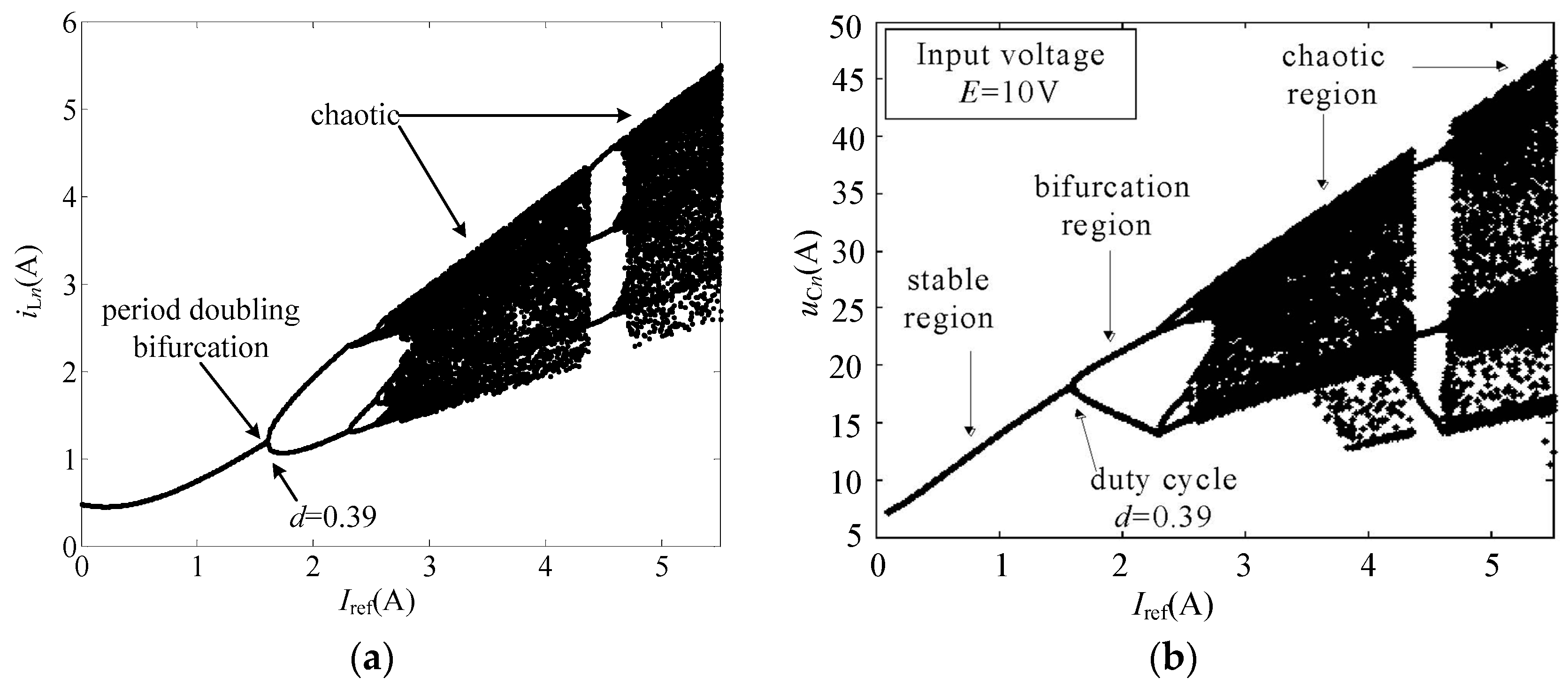
2. Typical Limitation of Boost Converter with Classical PCM Control Scheme

The circuit diagram of the boost converter is shown in Figure 1a, where rL, rC, and rT denote the parasitic resistances of the inductor, L, the capacitor, C, and the switch, ST, respectively. The control loop consists of a comparator, and an R-S flip-flop. The operation can be briefly described as follows. The flip-flop is set periodically by the clock signal, turning on the switch, ST. Then, the inductor current, iL, goes up linearly, and is compared with the reference level, Iref. When the peak value of iL reaches the level, Iref, the output of the comparator resets the flip-flop, thereby turning off ST. When ST is off, the inductor current falls almost linearly.
Assuming that the converter operates in CCM, there are two operating modes depending on whether or not ST is on, and typical waveforms of iL and the clock signal are shown in Figure 1b. The PCM-controlled boost converter can be described by:
{ x ˙ = A 1 x + B 1 E , n T s t < ( n + d n ) T s x ˙ = A 2 x + B 2 E , ( n + d n ) T s t < ( n + 1 ) T s ,
where E, Ts, and dn denote the input voltage, switching period, and duty ratio in the nth cycle, respectively. The state vector was set to be x = [iL, uO]Tr, where the superscript ‘Tr’ means the transposition of a matrix. The system matrices, Ai (i = 1, 2) and Bi (i = 1, 2), are given by:
A 1 = [ r T + r L L 0 0 1 C ( R + r C ) ] ,   A 2 = [ r L L 1 L R ( L r C r L C ) C ( R + r C ) L + R C r C L C ( R + r C ) ] ,
and:
B 1 = [ 1 L 0 ] ,   B 2 = [ 1 L R r C L ( R + r C ) ] .
A stroboscopic map is a discrete map or iterative map obtained by sampling a continuous system periodically, which describes the dynamics of a discrete variable in terms of a difference equation. According to (1), the stroboscopic map can be obtained as:
x n + 1 = F ( x n ,   I ref ) = Φ 2 ( ( 1 d n ) T s ) [ Φ 1 ( d n T s ) x n + Ψ 1 ( d n T s ) E ] + Ψ 2 ( ( 1 d n ) T s ) E ,
in which xn and xn+1 denote the state vector at the instant of t = nTs and t= (n + 1)Ts, respectively. Φi(ξ) and Ψi(ξ) are calculated by the following equations as:
Φ i ( ξ ) = e A i ( ξ ) = I + k = 1 1 k ! A i k ξ k , Ψ i ( ξ ) = 0 ξ Φ i ( τ ) B i d τ ,
where ‘I’ is a symbol of the unit matrix, and the subscript i = 1, 2. The switching function is defined as:
s ( x n ,   d n ) = d n ( I ref i Ln ) / m 1 T s ,
in which m1 = E/L is the rising slope of iL, and dn can be determined by setting the switching function to be zero, i.e., s(xn, dn) = 0.
Parameters of the converter are listed in Table 1, which were chosen to be the same as those in [32]. When Iref is changed from 0.5 to 5.5 A, typical bifurcation diagrams of iL and uC versus Iref can be obtained by numerical simulation. Bifurcation is the sudden change of the qualitative behavior of a system when one or more parameters are varied. Bifurcation literally means splitting into two parts. In nonlinear dynamics, the term has been used to mean the splitting of the behavior of a system at a threshold parameter value into two qualitatively different behaviors, corresponding to parameter values below and above the threshold. So, a bifurcation diagram is a summary chart of the behavioral changes as some selected parameters are varied. DC-DC converters are typically nonlinear, and the bifurcation diagram has become a very common tool for analysis of the dynamic behaviors of converters. It can be seen in Figure 2 that the period doubling bifurcation occurs at Iref = 1.52 A with d = 0.39 and the voltage set-up ratio M = 1.64. Along with the increase of Iref, the converter undergoes several period doubling bifurcations, and evolves into a chaotic state eventually. Obviously, when the system operates in a chaotic state, there are usually different kinds of values of uC corresponding to the same Iref. Then, it is desirable to stabilize the system from a chaotic state to the target period-1 orbit with larger uC, by some kind of chaotic control method, such as the method based on parameter perturbation.

3. An Improving Scheme Based on the Target UPO Tracking Method

3.1. Principle of the Parameter-Perturbation Method

The parameter-perturbation method is designed to stabilize a discrete chaotic system on a desired unstable period-1 orbit (UPO-1) [30]. For a two-dimensional discrete system, it can be described by the following equation as:
x n + 1 = F ( x n ,   p n ) ,
where F(·) is a smooth vector function, x R 2 is state vector of the system, P is a parameter that can be changed in a neighborhood of a nominal value of P [30], and the subscript n denotes the nth iteration. Assuming that the system is in chaotic state, and has an unstable fixed point, XP, the following equation can be obtained:
X P = F ( X P ,   P ) .
Then, in a sufficiently small neighborhood of XP, the system (Equation (7)) can be approximated by a linear map as:
x n + 1 = J x ( x n X P ) + J p ( p n P ) + X P ,
where the coefficient matrices, Jx and Jp, are defined as:
J x = F ( x n ,   p n ) x | ( X p ,   P ) ,   J p = F ( x n ,   p n ) p | ( X p ,   P ) .
According to Equation (9), two steps of perturbations are needed for the selected parameter, the iterative function for xn+2 can be obtained, that is:
x n + 2 = J x 2 ( x n X p ) + [ J x J p J p ] [ p n P p n + 1 P ] + X p ,
and it is the expression for the UPO-1 that corresponds to XP.
When the system is stabilized to the desired UPO-1, then xn+2 = xn+1 = XP, and the following perturbation increments for Pn can be acquired by:
[ Δ p n Δ p n + 1 ] = [ p n P p n + 1 P ] = [ J x J p J p ] 1 J x 2 ( X p x n ) = M ( X p x n ) .

3.2. Implementation Scenario

This subsection provides a scenario to illustrate the common functionality that can be implemented in a PCM-controlled boost converter. Based on dynamic analysis of the boost converter with a classical PCM control scheme, one ensures that the converter operates in a chaotic state when the reference level is set to be Iref = 3 A, and the other parameters are shown in Table 1. According to the basic principle of the parameter-perturbation method above, let xn+1 = xn in Equation (4), one can obtain the unstable fixed point as:
X p = [ I L p ,   U O p ] Tr = [ 2.4344 ,   26.2895 ] Tr .
The perturbing values for the reference current can be calculated according to Equation (12), and the reference current becomes:
I refn ( p ) = Δ I refn + I ref .
By using the above computed perturbations, the UPO-1 of the converter can be found, which will be in the form of Equation (11). The schematic diagram of the stabilizer can be designed. As shown in Figure 3, in addition to the conventional peak current mode control scheme, a perturbation module is added to generate the disturbance increments for the controlled parameter. Additionally, the reference level in each period is the sum of the nominal value, Iref, and the disturbance increments, ∆Irefn, which is calculated by the perturbation module at the beginning of the nth period according to Equation (14). The additional switch, S, in the control loop is used to enable and disable this target orbit control scheme.
Figure 4a,b respectively show the simulated time-domain waveforms and the phase trajectories of the state variables at Iref = 3 A. Obviously, it can be seen from Figure 4a that before t = 0.02 s, the conventional PCM-controlled boost converter operates in a chaotic state, with larger ripples accompanying the inductor current and output voltage. When the switch, S, is enabled at the instant of t = 0.02 s, the proposed control scheme comes into force. Additionally, the system can be stabilized quickly from the chaotic state to the desired target period-1 orbit (UPO-1), as shown in Figure 4b. Moreover, the peak-peak values of the inductor current and output voltage are reduced to 0.57 A and 5.5 V from 1.45 A and 15 V, respectively.

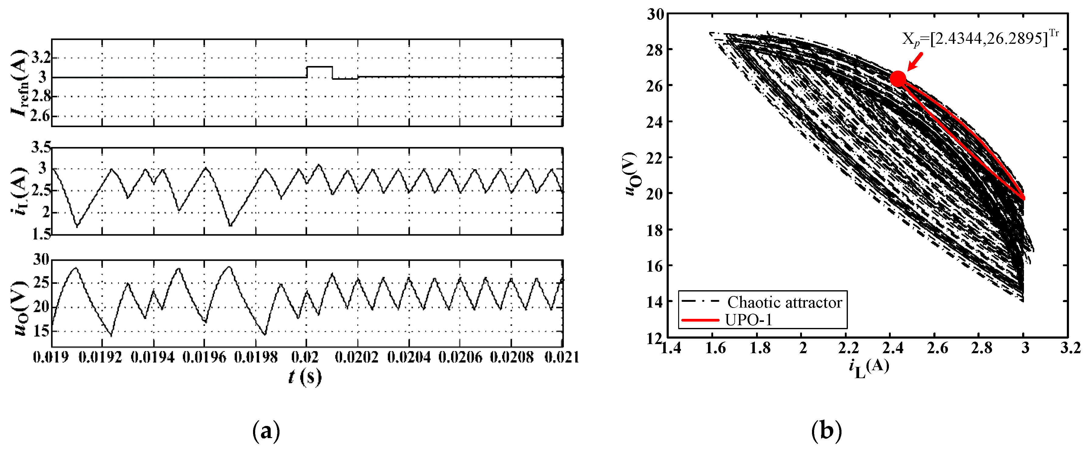
3.3. Performance Assessment

The performances of the converter can be evaluated by checking the movement of the eigenvalues when some chosen circuit parameters are varied. Any crossing from the interior of the unit circle to the exterior indicates a bifurcation. Particularly, if a real eigenvalue goes through −1 as it moves out of the unit circle, a period-doubling occurs.
According to the stroboscopic map of the boost converter, the Jacobian matrix evaluated in the neighborhood of Xp (the equilibrium point) is defined as:
J ( X p ) = F x n F d n ( s d n ) 1 s d n | x n = X p ,
one can get the following derivatives by using Equations (4) and (6):
F x n = Φ 2 ( ( 1 d n ) T s ) Φ 1 ( d n T s ) ,
F d n = T s Φ 2 ( ( 1 d n ) T s ) ( A 1 A 2 ) Φ 1 ( d n T s ) x n T s A 2 Φ 2 ( ( 1 d n ) T s ) A 2 1 B 2 E + Φ 2 ( ( 1 d n ) T s ) A 1 1 B 1 ,   E [ T s A 2 Φ 2 ( ( 1 d n ) T s ) + T s A 1 Φ 1 ( d n T s ) + T s A 2 ]
s d n = ( r L + r T ) T s L ( i L E r L + r T ) e r L + r T L d n T s ,
s d n = [ 0.5042 e r L + r T L d n T s ,   0.0002 ] .
Additionally, by introducing the above derivatives into Equation (15), it leads to the following characteristic equation as:
d e t ( λ I J ( X p ) ) = 0 .
Then, eigenvalues can be obtained by solving Equation (20).
When the reference level is set to be Iref = 3 A, the loci of eigenvalues of the converter with the proposed control technique is provided in Figure 5, in which the load and source disturbances are considered. For the variation of the load resistance, R, from 1 to 90 Ω, the loci of the eigenvalues can be obtained as shown in Figure 5a. From Figure 5a, the boost converter is stable when the load resistance is in the range of 1 to 57.4 Ω. The first point of period doubling bifurcation occurs at R = 57.4 Ω when one of the eigenvalues equals −1. After that, an eigenvalue moves out of the unit circle with the increase of the load resistance, R. For the variation of the input voltage, E, from 1 to 20 V, the loci of eigenvalues is depicted in Figure 5b. One can see that the converter is stable when the input voltage, E, is in the range of 4.95 to 20 V. Otherwise, the converter will be in an unstable state.
As a comparison, the loci of eigenvalues of the converter with the conventional PCM control technique is provided in Figure 6. It can be seen from Figure 6 that with the conventional PCM control scheme, the boost converter is stable for the load resistance being in the range of 1 to 3.06 Ω, and the source voltage, E, being in the range of 18.78 to 20 V.
From Figure 5 and Figure 6, the stable operating range for input disturbance is expanded remarkably from 18.78 to 20 V to 4.95 to 20 V, and similarly, the stable range for the load variation is also enlarged from 1 to 3.06 Ω to 1 to 57.4 Ω. Obviously, the performances of the classical PCM control scheme can be improved with the proposed stabilizer.

4. Comparison and Discussion

The general remedy to avoid the chaotic operation state of PCM-controlled converters is to introduce a compensating ramp to Iref. The basic circuit diagram of a PCM-controlled boost converter with ramp compensation and the typical steady-state waveforms are shown in Figure 7, where mc denotes the slope of the compensating signal.
According to the ramp compensation technique as shown in Figure 7, the reference current is given by the following equation:
I ref ( c ) = I ref m c ( t mod   T ) ,
where the term ‘t mod T’ means a modulo operation, which is equivalent with ‘t-kT’, and k is the integer quotient of t/T. Additionally, if the self-compensation technique in [25] is adopted, the reference can be described by:
I ref ( s ) = I ref 1 T 0 t [ I ref m 1 D T 2 i L ( τ ) ] d τ .
In Equations (21) and (22), m1 is the rising slope of the Boost converter. The reference current of the converter is set to be Iref = 3 A, and all the other circuit parameters are chosen as the same as those listed in Table 1. Additionally, to confirm that the converter with a constant slope of mc operates in a stable state, bifurcation analysis is performed. According to the results in Figure 8, period-doubling bifurcation occurs when mc = 3220 V/s. Then, in the following simulations, the value of mc is set to be 3250 V/s, and the converter can attain a higher voltage output than that in the case of mc > 3250 V/s.
To perform a comparison, both the conventional ramp compensation technique and the self- compensation technique are adopted in simulations. The behaviors and characteristics of the converter are put together with the proposed technique. The waveforms of applying different techniques to stabilize the PCM-controlled boost converter can be seen in Figure 9, where a transition from a chaotic state to a stable state is depicted.
In Figure 9, the red and black solid lines represent the reference current and the inductor current of the converter, respectively. It can be seen when stabilizers come into effect at t = 0.02 s, the converter with both the self-compensation technique and the proposed technique can be stabilized quickly. Yet, the converter with the conventional ramp compensation technique takes more than 20 switching cycles to enter a stable state.
Furthermore, the simulated stable current and voltage waveforms of the boost converter with different control strategies are provided in Figure 10. The black solid lines represent the results with the conventional ramp compensation technique, the blue dotted lines are obtained by using the self-compensation technique, and the red solid lines result from the proposed technique. It is seen that the three control techniques can be used to stabilize the converter from a chaotic state. Additionally, by setting UPO-1 as the control objective, the proposed technique can achieve a performance very close to that of using the self-compensation technique. However, the output voltage of the converter with the conventional ramp compensation technique is a little lower than those with the self-compensation technique and the proposed technique. Moreover, both the self-compensation technique and the proposed technique can ensure that the peak value of the inductor current does not deviate from the desired reference, whereas the conventional slope compensation technique cannot.
Additionally, with variations of the load from 2 to 80 Ω, and the input voltage from 0.5 to 20 V, respectively, the performances of the boost converter with three different kinds of control technique are compared, as listed in in Table 2. According to the simulation results summarized in Table 2, the boost converter has almost the same voltage gain under the proposed control technique and the self-compensation method. Both methods provide an accurate current limiting capacity, and their robustness is better than the conventional ramp compensation technique.

5. Experiments

In this section, experiments are performed, and the schematic diagram is shown in Figure 11. The experimental system includes the main circuit and the control loop, where the main circuit parameters are listed in Table 1. In the control loop, a hall sensor CSM050LX with the transfer ratio of 0.8 Ω is adopted to acquire the inductor current signal, so the value obtained from the oscilloscope should be divided by this coefficient. The amplifier AD620 is used to collect the output voltage signal. The conversion of A/D, and calculation of the disturbance increment of the controlled parameter are processed by an ARM-based 32-bit MCU (Microcontroller Unit) STM32F103C8T6. The 12-bit Digital-to-Analog Converter TLV5618 is adopted to perform the conversion of D/A. The voltage comparison and the RS flip-flop function are completed by LM339 and HD74LS02P, respectively. An optical coupler is used to drive the MOSFET, and it can also achieve the isolation between the main circuit and the control loop.
The experimental setup and the experimental results are shown in Figure 12. As shown in Figure 12b,c, the upper curves represent the inductor current and the lower curves represent the output voltage. The waveforms of the converter operating from the chaotic state to a stable state are shown in Figure 12a. The close-up views of the state variables in the chaotic and stable period-1 states are shown in Figure 12b,c respectively. It can be seen from Figure 12a that when the converter operates in the stable state, the sampling values for the inductor current at the bottom and peak point are 1.915 and 2.42 V, corresponding to the real inductor current values of 2.394 and 3.025 A, respectively. Additionally, the transfer ratio of the current sensor is 0.8 Ω. Thus, the peak-peak value of the inductor current is about 0.63 A. For the output voltage, as shown in Figure 12c, the valley and peak values are 18.78 and 25.01 V, respectively. It can also be seen from Figure 12 that when the converter returns to a stable state from a chaotic state, the peak-peak value of the output voltage is reduced to 6.228 from 13.56 V, and that of the inductor current is almost cut in half, i.e., from about 1.25 to 0.63 A.
Moreover, for the boost converter operating in a stable state with the proposed control scheme, a comparison of the data from both the simulation and experiment is summarized in Table 3. It should be noticed that the experimental value for the output voltage is about 1.3 V less than the simulated value, which is caused by the output diode. Thus, considering the conductance voltage drop of the Schottky diode, the experimental results agree quite well with the simulations. Another noteworthy thing is that in order to observe the effect of the proposed control method, the parameters of the example circuit, which result in the converter having larger ripples with the state variables, were chosen to be the same as those in [32].

6. Conclusions

A novel scheme for improving the classical PCM control method was presented in this paper, in which the principle of the parameter-perturbation method was introduced and adopted. The converter can be stabilized to operate in the target period orbit from the chaotic state. By applying this scheme to the DC-DC boost converter, the performances of the converter were improved, such as the converter’s stability range, the accuracy of current limiting, and so on. Moreover, compared to the conventional ramp compensation method, the proposed scheme demonstrated some advantages as follows. The transition time of the converter from the chaotic state to the steady state was greatly shortened. The capacity of the resisting load and source disturbances was expanded significantly, which means a better robustness was accomplished with the proposed control scheme. In addition to those mentioned above, the proposed method can achieve the same effect as the self-compensation method yet does not require an external signal generator for the ramp as in both the conventional ramp compensation and self-compensation scheme. The results from both simulations and experiments support the theoretical analysis, which indicates that the proposed technique can be used as an alternative to improve the performances of PCM-controlled DC-DC converters.

Author Contributions

Conceptualization, B.Z., and Y.C.; methodology, Y.C.; software, X.C., and Z.L.; validation, F.X.; formal analysis, X.C., and Z.L.; investigation, Z.L.; resources, B.Z., and D.Q.; data curation, F.X.; writing—original draft preparation, X.C., and Z.L.; writing—review and editing, Y.C., D.Q., and G.Z.; visualization, Y.C.; supervision, B.Z., and Y.C.; project administration, B.Z., and F.X.; funding acquisition, B.Z.

Funding

This research was funded by the Key Program of Natural Science Foundation of China, under Grant No.2018YFB0905804.

Conflicts of Interest

The authors declare no conflict of interest.

References

  1. Bernardo, M.; Budd, C.; Champneys, A.R.; Kowalczyk, P. Piecewise Smooth Dynamical Systems: Theory and Applications; Springer: London, UK, 2008. [Google Scholar]
  2. Leppäaho, J.; Suntio, T. Characterizing the Dynamics of the Peak-Current-Mode-Controlled Buck-Power-Stage Converter in Photovoltaic Applications. IEEE Trans. Power Electron. 2014, 29, 3840–3847. [Google Scholar] [CrossRef]
  3. Lu, W.; Lang, S.; Zhou, L.; Iu, H.H.; Fernando, T. Improvement of Stability and Power Factor in PCM Controlled Boost PFC Converter with Hybrid Dynamic Compensation. IEEE Trans. Circuits Syst. I 2015, 62, 320–328. [Google Scholar] [CrossRef]
  4. Tse, C.K. Complex Behavior of Switching Power Converters; CRC Press: New York, NY, USA, 2004. [Google Scholar]
  5. Tse, C.K.; Li, M. Design-oriented Bifurcation Analysis of Power Electronics Systems. Int. J. Bifurc. Chaos 2011, 21, 175–187. [Google Scholar] [CrossRef]
  6. Chen, Y.; Chi, K.T.; Qiu, S.S.; Lindenmuller, L.; Schwarz, W. Coexisting fast-scale and slow-scale instability in current-mode controlled DC/DC converters: Analysis, Simulation and Experimental Results. IEEE Trans. Circuits Syst. I 2008, 55, 3335–3348. [Google Scholar] [CrossRef]
  7. Yang, R.; Zhang, B.; Xie, F.; Iu HH, C.; Hu, W. Detecting bifurcation types in DC-DC switching converter by duplicate symbolic sequence and weight complexity. IEEE Trans. Ind. Electron. 2013, 60, 3145–3156. [Google Scholar] [CrossRef]
  8. Huang, L.; Qiu, D.; Xie, F.; Chen, Y.; Zhang, B. Modeling and Stability Analysis of a Single-Phase Two-Stage Grid-Connected Photovoltaic System. Energies 2017, 10, 2176. [Google Scholar] [CrossRef]
  9. Luo, Z.; Xie, F.; Zhang, B.; Qiu, D. Quantifying the Nonlinear Dynamic Behavior of the DC-DC Converter via Permutation Entropy. Energies 2018, 11, 2747. [Google Scholar] [CrossRef]
  10. Bao, B.; Zhou, G.; Xu, J.; Liu, Z. Unified Classification of Operation-State Regions for Switching Converters with Ramp Compensation. IEEE Trans. Power Electron. 2011, 26, 1968–1975. [Google Scholar] [CrossRef]
  11. Ma, W.; Wang, M.; Liu, S.; Li, S.; Yu, P. Stabilizing the average current-mode-controlled boost PFC converter via washout-filter-aided method. IEEE Trans. Circuits Syst. Express Briefs 2011, 58, 595–599. [Google Scholar] [CrossRef]
  12. Fan, J.W.T.; Chung, H.S.H. Bifurcation Phenomena and Stabilization with Compensation Ramp in Converter with Power Semiconductor Filter. IEEE Trans. Power Electron 2017, 32, 9424–9434. [Google Scholar] [CrossRef]
  13. Wang, Y.; Yang, R.; Zhang, B.; Hu, W. Smale horseshoes and symbolic dynamics in buck-boost DC-DC converter. IEEE Trans. Ind. Electron. 2018, 65, 800–809. [Google Scholar] [CrossRef]
  14. Suntio, T. Analysis and Modeling of Peak-Current-Mode-Controlled Buck Converter in DICM. IEEE Trans. Ind. Electron. 2001, 48, 127–135. [Google Scholar] [CrossRef]
  15. Suntio, T. Dynamic Profile of Switched-Mode Converter: Modeling, Analysis and Control; Wiley-VCH: Weinheim, Germany, 2009. [Google Scholar]
  16. Cha, H.; Peng, F.Z.; Yoo, D.W. Distributed Impedance Network (Z-Network) DC-DC Converter. IEEE Trans. Power Electron. 2010, 25, 2722–2733. [Google Scholar] [CrossRef]
  17. Hu, X.; Gong, C. A High Gain Input-Parallel Output-Series DC/DC Converter with Dual Coupled Inductors. IEEE Trans. Power Electron. 2015, 30, 1306–1317. [Google Scholar] [CrossRef]
  18. Zhang, G.; Zhang, B.; Li, Z.; Qiu, D.; Yang, L.; Halang, W.A. A 3-Z-Network Boost Converter. IEEE Trans. Ind. Electron. 2015, 62, 278–288. [Google Scholar] [CrossRef]
  19. Shen, H.; Zhang, B.; Qiu, D.; Zhou, L. A Common Grounded Z-Source DC-DC Converter with High Voltage Gain. IEEE Trans. Ind. Electron. 2016, 63, 2925–2935. [Google Scholar] [CrossRef]
  20. Shen, H.; Zhang, B.; Qiu, D. Hybrid Z-Source Boost DC-DC Converters. IEEE Trans. Ind. Electron. 2017, 64, 310–319. [Google Scholar] [CrossRef]
  21. Zhang, Y.; Liu, Q.; Li, J.; Sumner, M. A Common Ground Switched-Quasi-Z-Source Bidirectional DC-DC Converter with Wide-Voltage-Gain Range for EVs With Hybrid Energy Sources. IEEE Trans. Ind. Electron. 2018, 65, 5188–5200. [Google Scholar] [CrossRef]
  22. Shabestari, P.M.; Gharehpetian, G.B.; Riahy, G.H.; Mortazavian, S. Voltage controllers for DC-DC boost converters in discontinuous current mode. In Proceedings of the 2015 International Energy and Sustainability Conference (IESC), Farmingdale, NY, USA, 12–13 November 2015. [Google Scholar] [CrossRef]
  23. Hejri, M.; Mokhtari, H. Hybrid predictive control of a DC–DC boost converter in both continuous and discontinuous current modes of operation. Optim. Control Appl. Methods 2011, 32, 270–284. [Google Scholar] [CrossRef]
  24. Qian, T.; Lehman, B. An adaptive ramp compensation scheme to improve stability for DC-DC converters with ripple-based constant on-time control. In Proceedings of the 2014 IEEE Energy Conversion Congress and Exposition (ECCE), Pittsburgh, PA, USA, 14–18 September 2014; pp. 14–18. [Google Scholar] [CrossRef]
  25. Liu, P.H.; Yan, Y.; Lee, F.C.; Mattavelli, P. Universal Compensation Ramp Auto-tuning Technique for Current Mode Controls of Switching Converters. IEEE Trans. Power Electron. 2018, 33, 970–974. [Google Scholar] [CrossRef]
  26. Chen, W.W.; Chen, J.F.; Liang, T.J.; Wei, L.C.; Ting, W.Y. Designing a Dynamic Ramp with an Invariant Inductor in Current-Mode Control for an On-Chip Buck Converter. IEEE Trans. Power Electron. 2014, 29, 750–758. [Google Scholar] [CrossRef]
  27. El Aroudi, A.; Mandal, K.; Giaouris, D.; Banerjee, S. Self compensation of DC-DC converters under peak current mode control. Electron. Lett. 2017, 53, 345–347. [Google Scholar] [CrossRef]
  28. Cheng, W.; Song, J.; Li, H.; Guo, Y. Time-Varying Compensation for Peak Current-Controlled PFC Boost Converter. IEEE Trans. Power Electron. 2015, 30, 3431–3437. [Google Scholar] [CrossRef]
  29. Morcillo, J.D.; Burbano, D.; Angulo, F. Adaptive ramp technique for controlling chaos and subharmonic oscillations in DC-DC power converters. IEEE Trans. Power Electron. 2016, 31, 5330–5343. [Google Scholar] [CrossRef]
  30. Jimenez-Triana, A.; Chen, G.; Gauthier, A. A parameter-perturbation method for chaos control to stabilizing UPOs. IEEE Trans. Circuits Syst. II Express Briefs 2015, 62, 407–411. [Google Scholar] [CrossRef]
  31. Schöll, E.; Schuster, H.G. Handbook of Chaos Control, 2nd ed.; Wiley-VCH: Weinheim, Germany, 2008. [Google Scholar]
  32. Ayati, M. Chaos control of Boost converter via the fuzzy delayed-feedback method. In Proceedings of the 2016 4th International Conference on Control, Instrumentation, and Automation (ICCIA), Qazvin, Iran, 27–28 January 2016; pp. 324–328. [Google Scholar] [CrossRef]
Figure 1. Boost converter with a classical PCM control scheme: (a) Basic circuit diagram; (b) typical steady-state waveforms.
Electronics 08 01432 g001
Figure 2. Bifurcation diagram of a classical PCM-controlled boost converter: (a) For the inductor current iL versus Iref; (b) For the output capacitor voltage uC versus Iref.
Electronics 08 01432 g002
Figure 3. Circuit diagram of a PCM-controlled boost converter with a parameter-perturbation module.
Electronics 08 01432 g003
Figure 4. Simulations of the boost converter with the proposed control scheme: (a) Time-domain waveforms of state variables; (b) chaotic attractor and the stabilized UPO-1.
Electronics 08 01432 g004
Figure 5. Loci of eigenvalues of a PCM-controlled boost converter with the proposed technique: (a) Arrows indicate the direction of movement of the eigenvalues with R increasing, (b) Arrows indicate the direction of movement of the eigenvalues with E increasing.
Electronics 08 01432 g005
Figure 6. Loci of eigenvalues of the classical PCM-controlled boost converter: (a) Arrows indicate the direction of movement of the eigenvalues with R increasing; (b) Arrows indicate the direction of movement of the eigenvalues with E increasing.
Electronics 08 01432 g006
Figure 7. PCM-controlled boost converter with ramp compensation: (a) Basic circuit diagram; (b) typical steady-state waveforms.
Electronics 08 01432 g007
Figure 8. Bifurcation diagram of a PCM-controlled boost converter with constant ramp compensation.
Electronics 08 01432 g008
Figure 9. Stabilizing PCM-controlled boost converter by different techniques.
Electronics 08 01432 g009
Figure 10. Stable waveforms of the PCM-controlled boost converter with different techniques.
Electronics 08 01432 g010
Figure 11. Schematic diagram.
Electronics 08 01432 g011
Figure 12. (a) Experimental setup and experimental waveforms (channel 1: Inductor current iL; Channel 2: Output voltage uO): (b) From chaotic state to period-1 state, (c) chaotic operation, (d) period-1 operation.
Electronics 08 01432 g012
Table 1. Circuit parameters of the PCM-controlled boost converter.
ParametersValuesUnits
Input voltage E10V
Switching frequency f10kHz
Inductance L1mH
Capacitance C10μF
Load resistance R20Ω
On resistance rT50
Parasitic resistance rC30
Parasitic resistance rL40
Reference current Iref0.5 to 5.5A
Table 2. Comparison of performance quotas.
The Proposed TechniqueSelf-CompensationConventional Ramp Compensation
Duty cycle d0.56750.56610.5527
Voltage gain M2.31212.30472.2356
Peak values of iL3.0033 A3.0016 A2.8170 A
Transition time3 switching cycles6 switching cyclesmore than 20 switching cycles
Stable range for R(2 to 57.4) Ω(12.2 to 70) Ω(2 to 20.6) Ω
Stable range for E(4.95 to 20) V(5.96 to 20) V(10.1 to 20) V
Table 3. Results from simulation and experiment of the PCM boost converter with the proposed control.
ParametersSimulationExperiment
Duty cycle d0.56750.59
Voltage gain M2.312.19
Variation range of iL(2.43 to 3) A(2.394 to 3.025) A
Peak-peak value of inductor current iL0.57 A0.6312 A
Variation range of uO(19.5 to26.3) V(18.78 to 25.01) V
Peak-peak value of output voltage uO6.8 V6.228 V

