Generalized Cascaded Symmetric and Level Doubling Multilevel Converter Topology with Reduced THD for Photovoltaic Applications


SRM Institute of Science and Technology, Kattankulathur 603203, India
*
Author to whom correspondence should be addressed.
Electronics 2019, 8(2), 161; https://doi.org/10.3390/electronics8020161
Submission received: 1 October 2018
/
Revised: 31 December 2018
/
Accepted: 11 January 2019
/
Published: 1 February 2019
(This article belongs to the Special Issue Applications of Power Electronics)
Abstract
:In this paper, two different converter topologies for a basic new switched capacitor diode converter with a reduced number of power electronics components, suitable for grid connected photovoltaic applications were proposed. The two different structures of switched diode multilevel converter proposed were: (i) cascaded switched diode and (ii) cascaded switched diode with doubling circuit. The switched-diode multilevel converter was compared with other recent converters. In addition, a new dc offset nearest level modulation technique was proposed. This proposed dc offset technique offers low voltage total harmonic distortion (THD) and high RMS output voltage. The proposed modulation technique was compared with conventional nearest level modulation (NLM) and modified NLM control techniques. The performance of the proposed dc offset modulation technique was implemented using a FPGA Spartan 3E controller and tested with a novel switched capacitor-diode multilevel converter. However, to prove the authenticity of the switched-diode multilevel converter and modulation technique, a laboratory-based prototype model for 7-level and 13-level converters was developed.
1. Introduction
The multilevel converter is a promising power electronic converter for DC–AC high-power applications because it offers low electromagnetic interference (EMI), low dv/dt stress, and high efficiency. The conventional multilevel converters are (i) the neutral point clamped diode, (ii) flying capacitor, and (iii) cascaded H-bridge. The conventional multilevel converters have their own merits and demerits which are listed in References [1,2]. However, these conventional multilevel converters require a large number of power switches (IGBTs) for a higher number of levels, which is a major drawback. Many researchers are working towards the design of a novel multilevel converter with reduced power switches [3]. Several multilevel converters were recently proposed for are reduced number of dc sources and switches [4,5,6,7,8]. Another switched diode topology is presented in Reference [4], which requires single DC source and series connected DC-link capacitors to generate the maximum number of output voltage levels. These topologies have high blocking voltage stresses across the full bridge converter switches. To double the output voltage, a series of connected half-bridge circuits are presented in References [5,6]. These topologies produce a higher number of voltage levels with a greater number of switches and DC sources. The switched diode multilevel inverters for symmetric and asymmetric topologies with reduced DC sources and switches are presented in References [7,8]. Another recent topology is proposed with a lesser number of DC sources in Reference [9]. This topology generates a 11-level output. In order to increase the output voltage level, the cascaded connection is recommended. This topology produces a higher number of voltage levels with reduced switches, but it requires more isolated DC sources. The combined T-type and cross-connected topologies presented in Reference [10] with a self-capacitor voltage balancing. The proposed topology uses unidirectional switches and bidirectional switches without an anti-parallel diode. The presented topology requires a single DC source and multiple capacitors, therefore the switching complexity will increase as thenumber of levels increases. However, these topologies suffer from a greater number of power components like IGBTs, diodes, DC-link capacitors and complex pulse generation circuits. The full bridge inverter unit is used to change the polarity of the output voltage and current. As the number of levels increases, the voltage stress across the full bridge inverter with packed H-bridge inverter will also increase. This leads to many practical issues and hence increases the cost of the inverter [11].
The reduction of output voltage harmonics is still a challenge in power electronics DC/AC converters. In order to minimize the harmonics, different modulation techniques are developed by the researchers. The modulation techniques are classified into two categories: (i) low switching frequency and (ii) high switching frequency. The conventional modulation techniques are: multicarrier-based pulse width modulation (PD, POD, and APOD), hybrid modulation and hysteresis modulation. The multicarrier modulation technique will produce low THD by increasing the switching frequency, but it leads to high switching losses and a need for a complex cooling system which in turn degrades the reliability of the power switches. These modulation techniques are more suitable for medium power applications. For high power applications, low switching frequency modulation schemes are preferred. The low switching frequency modulation techniques are Nearest Space Vector Modulation (NSVM), Nearest Level Modulation (NLM) and space vector PWM (SVPWM) [12,13,14,15,16,17,18,19]. These modulation techniques produce low THD compared to conventional low switching frequency schemes, but the generation of gating pulses is more complicated as the number of level increases, except in the NLM technique. In addition, different offline PWM control strategies are employed for low switching frequency, which is used to find the optimum angles to minimize the harmonics in the output voltage [20,21]. However, these types of modulation techniques are used in open loop applications like uninterrupted power supplies (UPS), whereas it is not suitable for closed loop real-time applications like PV systems, since it takes more computational time.
The nearest level modulation technique [22] is another fundamental frequency method, which is operated at 50 Hz, but it is suitable for higher number of voltage levels. For a lower number of voltage levels, it produces high THD. The modified NLM technique has been presented [23], which has a DC offset value of 0.25 instead of 0.5 in the conventional NLM. The modified NLM increases the level and reduces the DC offset losses but is suitable for a modular multilevel converter. In this paper, a new multilevel converter with optimum nearest level modulation technique is presented. The DC offset value is chosen so that it minimizes the THD for a lower number of levels and increases the RMS voltage up to 17th level. This paper is organized as follows: In Section 2, the new multilevel converter basic unit is proposed with the various modes of operation. In order to increase the number of output voltage level, a cascaded connection of basic unit with and without half-bridge converter are presented and a comparison of the proposed multilevel converter with other recent topologies is made. In Section 3 Analysis of the proposed NLM technique with suitable illustrations is presented and the comparison of proposed modulation technique with other modulation methods is discussed. In Section 4 Experimental results are presented to confirm the objective of this paper. In Section 5 a suitable application and the advantages of the proposed methods are highlighted, in the Conclusions.
2. Proposed Multilevel Converter
2.1. Proposed Basic Unit
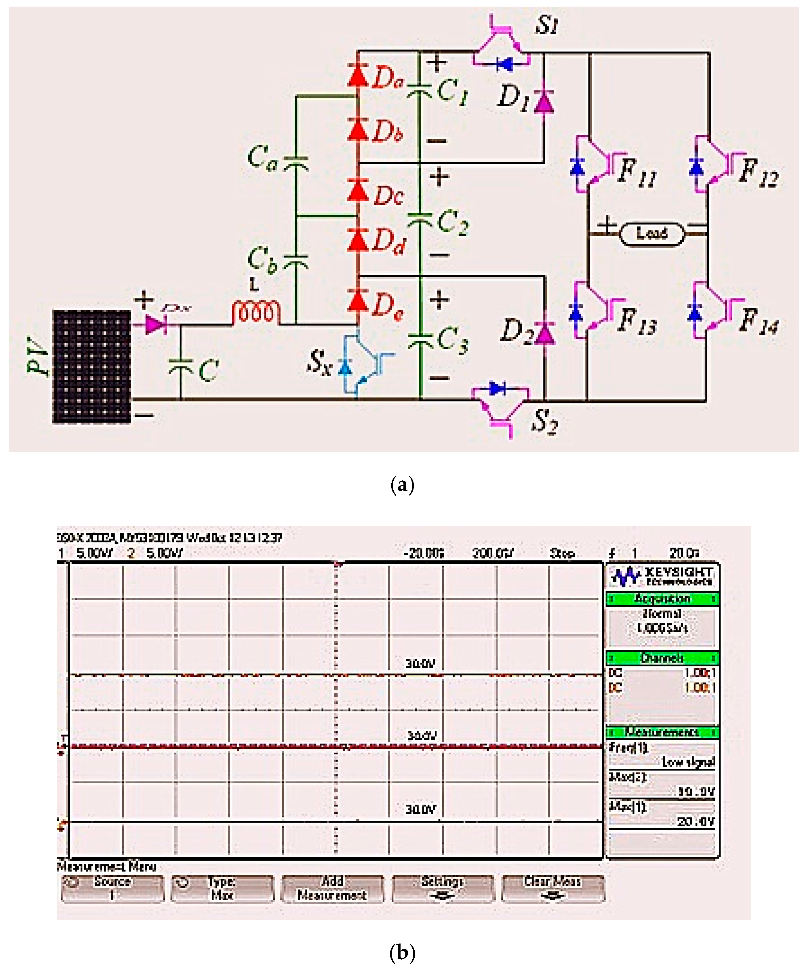
Figure 1 shows the proposed basic unit of the multilevel converter which consists of a single DC source with three DC-link capacitors (C1, C2, and C3) connected parallel to the source. The upper and lower capacitor voltages were tapped through switches S1 and S2. Floating capacitor C2 provides the current through diodes D1 and D2. The full bridge circuit (F11–F14) was used to alter the polarity of both the voltage and current paths through the load. Since the topology is symmetric, and it generates a maximum of seven levels of output voltage. The switch pairs (F11, F13) and (F12, F14) were not turned on simultaneously to avoid short circuit. The switching sequence for the basic unit is given in Table 1 and various modes of operation are illustrated in Figure 2.
Mode 0: The switch pairs, either (F11, F12) or (F13, F14), were turned on to produce the zero state. Mode 1: Diodes D1 and D2 were made to conduct to produce the level one output voltage level from the floating capacitor C2. Mode 2: The floating capacitor C2 was added with either a upper or lower capacitor by switching the S1 or S2 to generate the second level. Mode 3: Both S1 and S2 switches were turned on simultaneously to produce the level-3 voltage by connecting all the capacitors together. The full bridge converter switches (F11, F14) were turned on for the positive half cycle as shown in Figure 2a–c, and (F12, F13) were turned on for the negative half cycle in Figure 2d–f. Furthermore, the DC-link capacitor voltage balancing is another serious problem in series connected capacitors. This balancing was done either by switching techniques or by providing external circuits. In this paper, an external circuit, proposed in References [22,23], was used for balancing the capacitors.
2.2. Proposed Cascaded Topologies
The basic unit given was able to generate a maximum of 7-level output voltage with six switches and two diodes. To generate a higher number of voltagelevels, two different cascaded topologies were proposed and these topologies were named as switched capacitor-diode (SCDCAS) cascaded multilevel converter, where CAS referred to cascaded topology.
The first topology given in Figure 3a consists of a series connection of “n” number of basic units and each unit requires a separate DC source with three dc-link capacitors. In unit-1, capacitor voltages were named as V11, V12,V13. In unit-2 as V21,V22, V23 and in nth unit as Vn1, Vn2, Vn3. The maximum blocking voltage on the switches was the sum of all these dc source values. Another topology as a switched-diode half-bridge (SCDHBCAS) multilevel converter and is shown in Figure 3b. The half-bridge inverter was cascaded with a series connection of basic units to double the output voltage level.
The expression to find the number of levels, number of switches, isolated dc sources, capacitors, maximum blocking voltage and total blocking voltage are given in Table 2. These topologies can also be configured in the asymmetric mode, but in this paper only symmetric configuration was considered. The output voltage of SCDHBCAS topology was double that of the SCDCAS topology with minimum switches. The SCDHBCAS topology requires additional dc sources and reduce output voltage magnitude because the half-bridge circuit output voltage was always half that of the input voltage.
The topologies presented in References [5,6,7,8] were considered for the comparison and are shown in Figure 4. Total blocking voltage was one of the important parameters that decides the cost of the converter. If the blocking voltage was less, the cost of the switch would be lower. As shown in Figure 4a, the proposed topology SCDHBCAS has a lower total blocking voltage than the other topologies. In other words, the number of level was higher with reduced blocking voltage. The DC source is another parameter to be considered while designing a multilevel converter. From Figure 4b it is evident that the topologies referred in [7,8] requires more number of sources than the proposed converters. In Figure 4c, the number of switches is plotted against the number of levels. The proposed topology SCDHBCAS requires a minimum number of switches when compared to other topologies.
3. Modified DC-Offset Value in the NLM Method
The conventional NLM technique was more suitable for a higher number of levels because it produced a higher THD for a lower number of levels [2]. To get better THD and RMS output voltage, the optimum nearest modulation technique was proposed. In the NLM technique, the DC offset value was 0.5 (also called a half integer type), but in the case of optimal nearest level modulation (ONLM), the DC offset value was changed from 0.5 to 0.4.
where NLevel was the number of output levels and ‘ma’ was the modulation index. The output voltage for various modulation indices was calculated using Equation (1), where x1, x2 and x3 were the variables and this was compared with the voltage reference signal, to generate the pulses as shown in Figure 4. The intersection of reference signal and variables x1, x2 and x3 gavedifferent pulse widths with a duty cycle of D1, D2 and D3. The voltage RMS of the converter depends on the duty cycle of the switches.
Vout = ma × (NLevel − 1)/2 × Vdc × cos (ωt)
Here, the D3 has maximum duty cycle when compared with D2 and D1. Each intersection point gave a different switching angle θ1, θ2 and θ3 as shown in Figure 5. The variables x1, x2 and x3 directly affected the switching angle and duty cycle. The mathematical expression to find the RMS value was given in Equation (2).
T was the time period of the pulse from zero and V(t) was the magnitude of voltage. For simplicity V(t) was replaced by ‘a’ and Equation (3) is rewritten as:
Equation (3) was the voltage RMS of the pulses. RMS voltage for multilevel output was calculated by choosing the duty cycle of each level and multiplied with corresponding magnitude as discussed below:
The magnitude between each level was symmetric and hence a1 = a2 = a3 = … an = Vdc.
The switching angle calculation for the proposed modulation technique was given below:
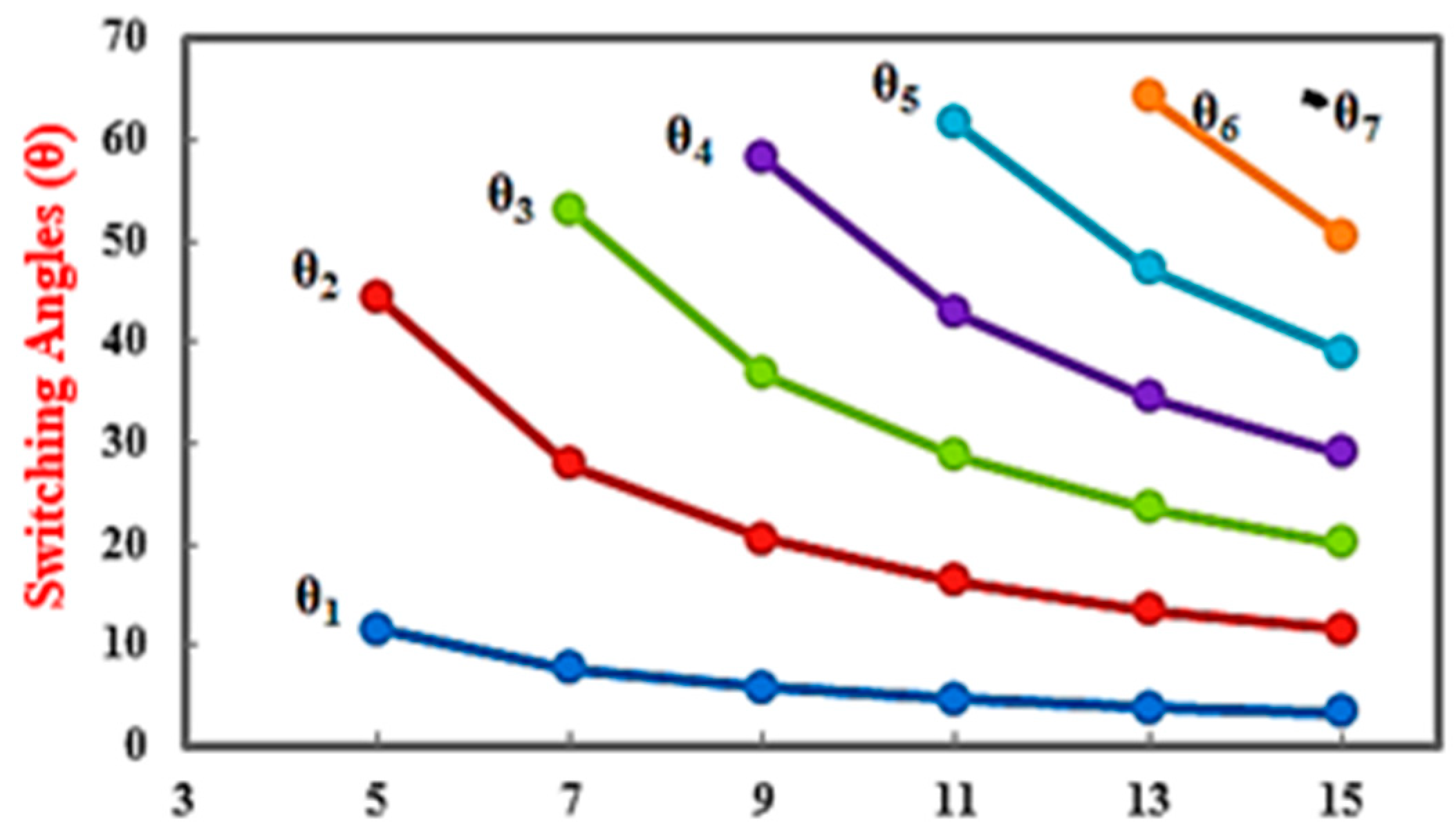
‘m’ is the number of levels. The different switching angle against the number of levels is shown in Figure 6. In this, if the number of level is increased, the switching angle (θ) value is reduced gradually. The key variables x1, x2 and x3 decides the switching angles and duty cycles. Instead of x1, x2 and x3 variables, constant DC offset was used in the modulation techniques. The DC offset value of 0.5 was used in the conventional NLM technique which is more suitable for a higher number of output voltage levels, but for lower voltage levels it produces high THD.
The functional block diagram of the proposed system is shown in Figure 7a To minimize the THD in lower numbers of levels, a new DC offset value of 0.4 was proposed. The reason for choosing 0.4 as the DC offset was illustrated in Figure 7b with a reference waveform. The magnitude of individual harmonics orders is presented on the left side of the Y axis and on the right side, variations of voltage RMS were presented in per unit value. The X-axis was the variation of DC offset which is varied from 0.1 to 0.9. Up to the 15th odd harmonics orders were considered for selection of DC offset value.
The lower order harmonics like 3rd, 5th and 7th were lower in the region of DC offset from 0.4 to 0.5. The 3rd order harmonic voltage was low, whereas the RMS voltage was high for a DC offset of 0.4. Therefore, a DC offset of 0.4 was considered optimum in this paper. This DC offset value was valid for a lower number of output voltage levels, up to the 17th-level. In the half integer type method (conventional NLM), the error (DC losses) between the two levels was always maintained at 0.5Vdc. In the proposed method, the error was minimized to 0.4Vdc, as shown in Figure 7c. The RMS value of the output voltage and current was higher than the conventional methods.
4. Simulation and Experimental Results
In this, the FPGA Spartan 3E was used to generate the pulse for the proposed converter. In terms of hardware, the RC delay circuit was used to provide the dead time of 2 µs between the pulses to avoid short circuit. The subsystem of the PV Simulink module is shown in Figure 8. This PV model was designed based on a single diode model as used in Reference [19]. In this model, the temperature is kept at 298 K and due to the variations in irradiance; the output voltage and current were varied. To extract the maximum power from the PV panel, the basic perturb and observe MPPT method was implemented and the regulated output voltage was obtained. However, this is not in the scope of this paper. The PV model consists of one diode for cell polarization and series/shunt resistance for the losses. The Ipv (Vpv) of this model was calculated as follows:
Rs and Rsh were series and shunt resistance, Iph was the photocurrent, Io was the reverse saturation current of the diode, q was the electron charge, K was constant, Tj was the junction temperature of the panel, Id was the intrinsic diode current, and Vpv and Ipv was the voltage and current in the panel. The DC/DC converter boosts the voltage from 40 V to 82 V. As per the single-phase grid, standard voltage is .
Ipv = Iph − Id − IRsh
The multilevel inverter output peak voltage was given below:
- Vpp = 3 × 110 = 330 V, Vrms = Vpp/sqrt (2)
- Vrms = 330/sqrt (2) = 232.2 V
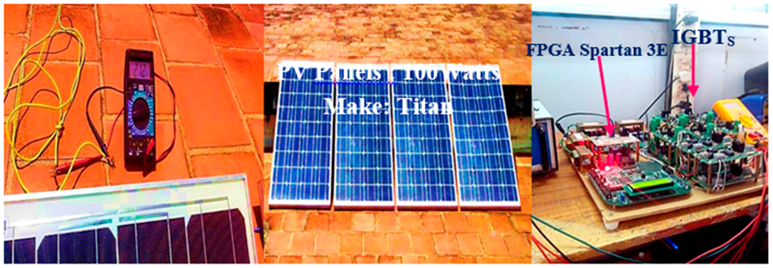
To prove the dynamic performance of the proposed topology, the modulation scheme was implemented using MATLAB/Simulink and experimentally verified with the hardware developed. The details of the PV panel and other hardware ratings were listed in Table 3.
4.1. Seven Level Inverter
The proposed 7-level inverter with voltage balancing circuit is shown in Figure 9a along with its balance output voltage in Figure 9b. To determine the performance of the multilevel inverter and modulation technique, the dynamic (without DC/DC converter) and steady-state output voltage (with DC/DC converter) were shown in Figure 10a–i for different irradiance values. In the basic unit, the DC/DC boost converter was used to regulate the output voltage to 90 V and each capacitor was balanced to 30 V; when the full irradiance was present with a minimum duty ratio of 0.12. The corresponding output voltage and current waveforms are shown in Figure 10a. The current THD depended on the load inductance value, because this acted as a low pass filter to produce a sinusoidal waveform, but here the resistance value is higher than the inductance value. Here it is worth mentioning that the voltage THD of the proposed modulation technique was 11.81% as shown in Figure 10c, which was higher than in Reference [21]. It was confirmed that the proposed modulation technique was suitable for a lower number of voltage levels with increased output RMS voltage. To regulate the PV output voltage, the non-isolated DC/DC converter was used. The experimental output voltage and current waveforms were shown in Figure 11 with the THD spectrum. The load resistance was 150 Ω and inductance was 70 mH which gives the maximum output power of 20.938 W with a power factor of 0.89 as shown in Figure 11b. The voltage RMS of the 7-level inverter was 65.11 V and current RMS was 0.36 A, which was higher than the theoretical value of 63.63 for given input.
4.2. Thirteen-Level Inverter
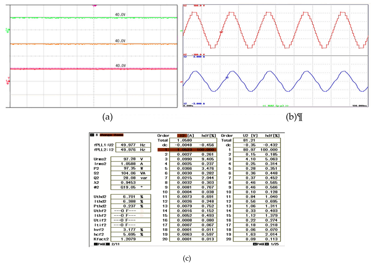
In this configuration the SCDHBCAS topology was used to generate the 13th-level. Each DC link capacitors voltage were regulated to 40 V and the half-bridge inverter voltage was 20 V.
For the 13-level inverter the maximum voltage RMS value was 126.28 V and current RMS was 1.05 A with a power factor of 0.94. The maximum output power was 86.35 W with the boost converter duty ratio of 0.35 to maintain the output voltage at 120 V with each DC-link capacitor voltage of 40 V, as shown in Figure 12a.The corresponding inverter output voltage and current waveforms were shown in Figure 12b. Voltage THD was 6.701% and current THD was 6.388%, the power factor was 0.94 which is close to unity, as illustrated in Figure 12c,d. In Figure 13, different loading conditions were used and the corresponding outputs were captured using DSO. In this way, the load values were changed ranging from purely resistive to inductive and a combination of both as illustrated in Figure 13a. A zoomed view of the load changes considered is shown in Figure 13b.
The proposed NLM technique produced high voltage RMS of 97.28 V, whereas 98.85 V was the theoretical value. From the proposed modulation it was confirmed that it generates low THD and high voltage RMS for a lower number of levels. The laboratory-based prototype model of the proposed multilevel converter for the 13th-level is shown in Figure 14 with PV as the input source.
5. Conclusions
The generalized cascaded multilevel converter was proposed with the optimum nearest level modulation technique in this paper. Basic units and the cascaded connection of basic units were discussed with half-bridge and without half-bridge circuits. With the half-bridge converter, it produced the maximum output voltage for higher voltage levels than it did without the half-bridge circuit. The proposed modified nearest level modulation technique was presented which generated the low THD and high voltage RMS. The experimental validation of the proposed converter and modified NLM technique was compared with the simulation results. The modified NLM technique was proved to be more suitable for a lower number of output voltage levels and was found suitable for photovoltaic applications.
Author Contributions
K.D: design, analysis, simulation and hardware implementation of proposed system; V.K: comparison and validation of results; J.S.M: formatting and English editing.
Funding
This research received no external funding.
Conflicts of Interest
The authors declare no conflict of interest.
References
- Rodriguez, J.; Lai, J.-S.; Peng, F.Z. Multilevel inverters: A survey of topologies, controls, and applications. IEEE Trans. Ind. Electron. 2002, 49, 724–738. [Google Scholar] [CrossRef]
- Franquelo, L.G.; Rodriguez, J.; Leon, J.I.; Kouro, S.; Portillo, R.; Prats, M.A.M. The age of multilevel converters arrives. IEEE Trans. Ind. Electron. Mag. 2008, 2, 28–39. [Google Scholar] [CrossRef]
- Gupta, K.; Ranjan, A.; Bhatnagar, P.; Sahu, L.; Jain, S. Multilevel Inverter Topologies with Reduced Device Count: A Review. IEEE Trans. Ind. Electron. 2016, 31, 135–151. [Google Scholar] [CrossRef]
- Lee, S.S. Single-Stage Switched-Capacitor Module (S3CM) Topology for Cascaded Multilevel Inverter. IEEE Trans. Power Electron. 2018, 33, 8204–8207. [Google Scholar] [CrossRef]
- Liu, J.; Cheng, K.W.E.; Ye, Y. A Cascaded Multilevel Inverter Based on Switched-Capacitor for High-Frequency AC Power Distribution System. IEEE Trans. Power Electron. 2014, 29, 4219–4230. [Google Scholar] [CrossRef]
- Ye, Y.; Cheng, K.W.E.; Liu, J.; Ding, K. A Step-Up Switched-Capacitor Multilevel Inverter with Self-Voltage Balancing. IEEE Trans. Ind. Electron. 2014, 61, 6672–6680. [Google Scholar] [CrossRef]
- Taghvaie, J.A.; Rezanejad, M. A Self-Balanced Step-Up Multilevel Inverter Based on Switched-Capacitor Structure. IEEE Trans. Power Electron. 2018, 33, 199–209. [Google Scholar] [CrossRef]
- Barzegarkhoo, R.; Moradzadeh, M.; Zamiri, E.; Kojabadi, H.M.; Blaabjerg, F. A New Boost Switched-Capacitor Multilevel Converter with Reduced Circuit Devices. IEEE Trans. Power Electron. 2018, 33, 6738–6754. [Google Scholar] [CrossRef]
- Raman, S.R.; Cheng, K.W.E.; Ye, Y. Multi-Input Switched-Capacitor Multilevel Inverter for High-Frequency AC Power Distribution. IEEE Trans. Power Electron. 2018, 33, 5937–5948. [Google Scholar] [CrossRef]
- Liu, J.; Wu, J.; Zeng, J. Symmetric/Asymmetric Hybrid Multilevel Inverters Integrating Switched-Capacitor Techniques. IEEE J. Emerg. Sel. Top. Power Electron. 2018, 6, 1616–1626. [Google Scholar] [CrossRef]
- Prabaharan, N.; Palanisamy, K. Analysis of cascaded H-bridge multilevel inverter configuration with double level circuit. IET Power Electron. 2017, 10, 1023–1033. [Google Scholar] [CrossRef]
- Carrara, G.; Gardella, S.; Marchesoni, M.; Salutari, R.; Sciutto, G. A new multilevel PWM method: A theoretical analysis. IEEE Trans. Power Electron. 1992, 7, 497–505. [Google Scholar] [CrossRef]
- McGrath, B.P.; Holmes, D.G. Multicarrier PWM strategies for multilevel inverters. IEEE Trans. Ind. Electron. 2002, 49, 858–867. [Google Scholar] [CrossRef]
- Franquelo, L.G.; Prats, M.A.M.; Portillo, R.C.; Galvan, J.I.L.; Perales, M.A.; Carrasco, J.M.; Diez, E.G.; Jimenez, J.L.M. Three dimensional space-vector modulation algorithm for four-leg multilevel converters using ABC coordinates. IEEE Trans. Ind. Electron. 2006, 53, 458–466. [Google Scholar] [CrossRef]
- McGrath, B.P.; Holmes, D.G.; Lipo, T. Optimized space vector switching sequences for multilevel inverters. IEEE Trans. Power Electron. 2003, 18, 1293–1301. [Google Scholar] [CrossRef]
- Govindaraju, C.; Baskaran, K. Efficient Sequential Switching Hybrid-Modulation Techniques for Cascaded Multilevel Inverters. IEEE Trans. Power Electron. 2011, 26, 1639–1648. [Google Scholar] [CrossRef]
- Shukla, A.; Ghosh, A.; Joshi, A. Hysteresis Modulation of Multilevel Inverters. IEEE Trans. Power Electron. 2011, 26, 1396–1409. [Google Scholar] [CrossRef]
- Rahim, N.A.; Selvaraj, J.; Chaniago, K. A novel PWM multilevel inverter for PV application. IEICE Electron. Express 2009, 6, 1105–1111. [Google Scholar] [CrossRef] [Green Version]
- Rekioua, D.; Matagne, E. Optimization of Photovoltaic Power Systems, Modelization, Simulation and Control; Springer: London, UK, 2012; pp. 31–87. [Google Scholar]
- Rathore, A.K.; Holtz, J.; Boller, T. Synchronous optimal pulsewidth modulation for low-switching-frequency control of medium-voltage multilevel inverters. IEEE Trans. Ind. Electron. 2010, 57, 2374–2381. [Google Scholar]
- Rathore, A.; Holtz, J.; Boller, T. Generalized optimal pulsewidth modulation of multilevel inverters for low-switching-frequency control of medium-voltage high-power industrial ac drives. IEEE Trans. Ind. Electron. 2013, 60, 4215–4224. [Google Scholar] [CrossRef]
- Karthikeyan, D.; Krishnasamy, V.; Sathik, M.A.J. Development of a switched diode asymmetric multilevel inverter topology. J. Power Electron. 2018, 18, 418–431. [Google Scholar]
- JagabarSathik, M.A.; Abdel Aleem, S.H.E.; Kannan, R.; Zobaa, A.F. A New Switched DC-Link Capacitor-based Multi-level Converter (SDC2MLC). Electr. Power Compon. Syst. 2017, 45, 1001–1015. [Google Scholar] [CrossRef]
Figure 1.
Proposed basic unit.

Figure 2.
(a–f) Various modes of operation of the proposed basic unit.

Figure 3.
Proposed switched-diode cascaded topology; (a) without doubling circuit and (b) with doubling circuit.
Figure 3.
Proposed switched-diode cascaded topology; (a) without doubling circuit and (b) with doubling circuit.

Figure 4.
Comparison of proposed multilevel converter with other topologies (a) NSwitches vs. NLevel; (b) TBVp.u vs. NLevel and (c) NLevel vs. Nsource.
Figure 4.
Comparison of proposed multilevel converter with other topologies (a) NSwitches vs. NLevel; (b) TBVp.u vs. NLevel and (c) NLevel vs. Nsource.

Figure 5.
Variation of duty cycle with respect to DC offset value x1, x2 and x3.

Figure 6.
Number of levels vs switching angle.

Figure 7.
(a) A functional block diagram of the proposed system (b) DC offset 0.4 compared with reference waveform and pulse generation method; (c) the various DC offset values with corresponding THD.
Figure 7.
(a) A functional block diagram of the proposed system (b) DC offset 0.4 compared with reference waveform and pulse generation method; (c) the various DC offset values with corresponding THD.
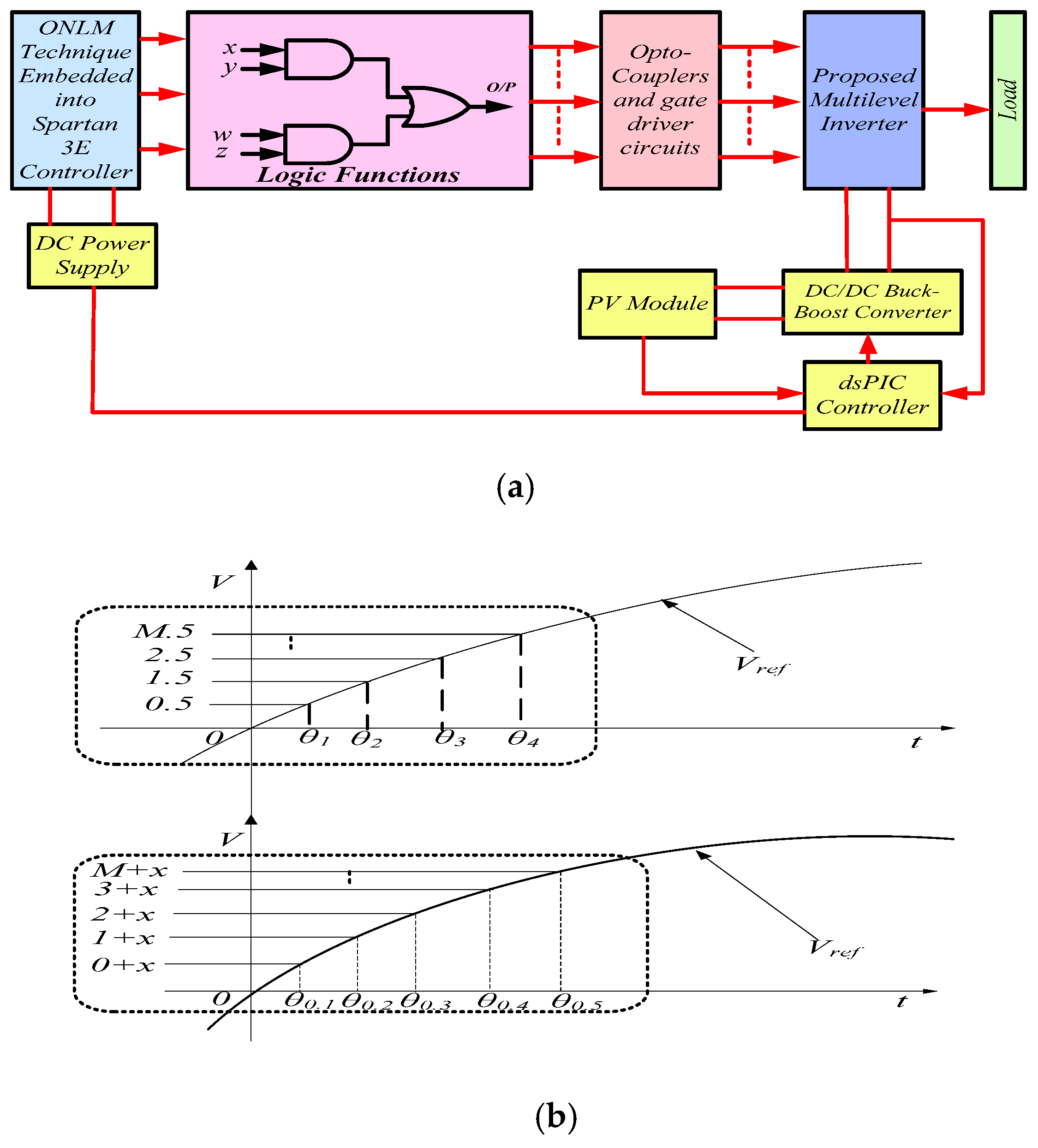
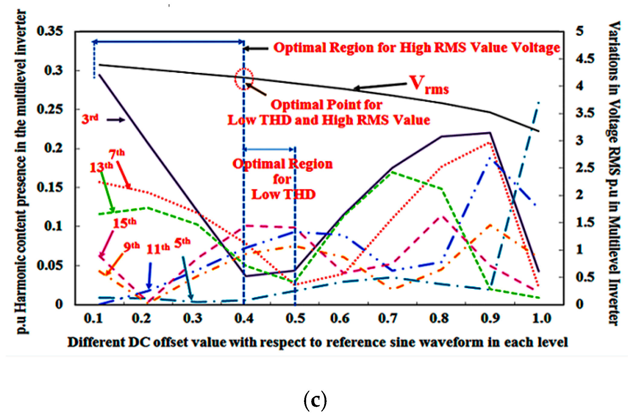
Figure 8.
Simulation of PV module.
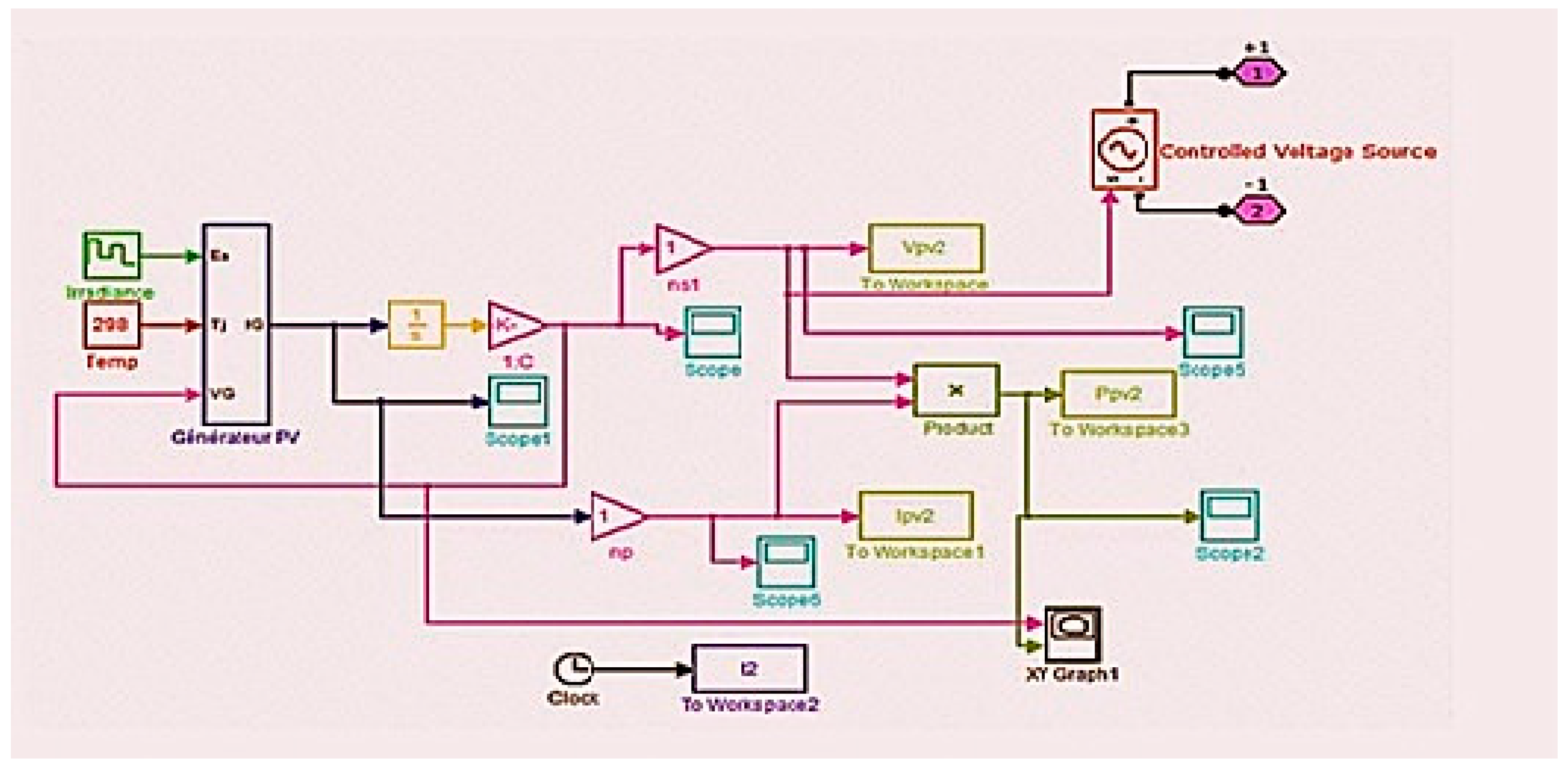
Figure 9.
(a) Proposed seven-level inverter with voltage balancing circuit. (b) Proposed capacitor balancing circuit output voltage.
Figure 9.
(a) Proposed seven-level inverter with voltage balancing circuit. (b) Proposed capacitor balancing circuit output voltage.

Figure 10.
Multilevel inverter voltage waveform (a) without voltage balancing circuit; (b) with voltage balancing circuit; (c) steady-state voltage, multilevel inverter current waveform and (d) without voltage balancing circuit; (e) with voltage balancing circuit; (f) steady-state current; (g) current and voltage across the H-bridge switches; (h) output voltage and (i) variation in irradiance.

Figure 11.
Experimental results for 7-level inverter (a) output voltage and current waveform (b) output from power quality analyzer and (c) voltage harmonics.
Figure 11.
Experimental results for 7-level inverter (a) output voltage and current waveform (b) output from power quality analyzer and (c) voltage harmonics.

Figure 12.
Experimental results of thirteen-level converter (a) capacitor voltages after balancing (b) output voltage and current waveform and (c) voltage harmonics.
Figure 12.
Experimental results of thirteen-level converter (a) capacitor voltages after balancing (b) output voltage and current waveform and (c) voltage harmonics.

Figure 13.
Experimental results of thirteen-level converter; (a) different loading conditions and (b) zoomed view of load changes.
Figure 13.
Experimental results of thirteen-level converter; (a) different loading conditions and (b) zoomed view of load changes.

Figure 14.
Photograph of experimental setup.


Table 1.
Switching sequence for the basic unit.
| State | On State Switches | Full Bridge Switches | Output Voltage Level |
|---|---|---|---|
| 0 | − | F11,F12 | 0 V |
| F13,F14 | |||
| 1 | D1, D2 | F11,F14 | +Vdc/3 |
| F12,F13 | −Vdc/3 | ||
| 2 | (S1, D2) or (S2, D1) | F11,F14 | +2Vdc/3 |
| F12,F13 | −2Vdc/3 | ||
| 3 | S1, S2 | F11,F14 | +Vdc |
| F12,F13 | −Vdc |
Table 2.
Comparison of power components in the proposed topologies.
| S.No | Various Parameters | (SCDCAS) Topology | (SCDHBCAS) Topology |
|---|---|---|---|
| 1. | NLevel | 6n + 1 | 12n + 1 |
| 2. | NSwitches | 6n | 6n + 2 |
| 3. | Ndiode | 2n | 2n |
| 4. | Ncapacitors | 3n | 3n + 1 |
| 5. | Nsource | n | N + 1 |
| 6. | Maxblock | Vdc | Vdc |
| 7. | Tblock | n6 Vdc | (6n + 2) Vdc |
Table 3.
Parameters used for hardware.
| Description | Specifications |
| PV System | |
| PV Model 12100 | 04 Nos |
| Open Circuit Voltage | 26.8 V |
| Short Circuit Current | 6.2 A |
| Maximum Voltage (Vm) | 21.8 V |
| Maximum Current (Im) | 5.62 A |
| Maximum system DC Voltage | 1000 V |
| Power Tolerance | ±5% |
| Load | |
| Resistance (R) | 150 Ω & 80 Ω |
| Inductor (L) | 70 mH & 80 mH |
| Multilevel Converter | |
| IRF 460 500 V/21 A | 06 & 08 Nos |
| Gate Driver-HCPL316j | 06 & 08 Nos |
| Capacitors | 150 µF |
| FPGA Spartan3E | 1 |
| Snubber Circuits | RCD |
| Results | |
| Output Voltage | 90 V & 120 V |
| Output Current | 0.5 A & 1.51 A |
© 2019 by the authors. Licensee MDPI, Basel, Switzerland. This article is an open access article distributed under the terms and conditions of the Creative Commons Attribution (CC BY) license (http://creativecommons.org/licenses/by/4.0/).
Share and Cite
MDPI and ACS Style
D, K.; K, V.; M, J.S. Generalized Cascaded Symmetric and Level Doubling Multilevel Converter Topology with Reduced THD for Photovoltaic Applications. Electronics 2019, 8, 161. https://doi.org/10.3390/electronics8020161
AMA Style
D K, K V, M JS. Generalized Cascaded Symmetric and Level Doubling Multilevel Converter Topology with Reduced THD for Photovoltaic Applications. Electronics. 2019; 8(2):161. https://doi.org/10.3390/electronics8020161
Chicago/Turabian StyleD, Karthikeyan, Vijayakumar K, and Jagabar Sathik M. 2019. "Generalized Cascaded Symmetric and Level Doubling Multilevel Converter Topology with Reduced THD for Photovoltaic Applications" Electronics 8, no. 2: 161. https://doi.org/10.3390/electronics8020161
Note that from the first issue of 2016, this journal uses article numbers instead of page numbers. See further details here.