Perylene-Diimide Molecules with Cyano Functionalization for Electron-Transporting Transistors
by
 , ,
, ,
Mario Barra
1 ,
,
Fabio Chiarella
1,*,
Federico Chianese
2,1,
Ruggero Vaglio
2,1 and
Antonio Cassinese
2,1 1
CNR-SPIN, c/o Dipartimento di Fisica “Ettore Pancini”, P.le Tecchio, 80, I-80125 Naples, Italy
2
Physics Department “Ettore Pancini”, University of Naples ‘Federico II’, P.le Tecchio, 80, I-80125 Naples, Italy
*
Author to whom correspondence should be addressed.
Electronics 2019, 8(2), 249; https://doi.org/10.3390/electronics8020249
Submission received: 30 January 2019
/
Revised: 14 February 2019
/
Accepted: 18 February 2019
/
Published: 22 February 2019
(This article belongs to the Special Issue Organic Semiconductors and Their Electronic Application)
Abstract
:Core-cyanated perylene diimide (PDI_CY) derivatives are molecular compounds exhibiting an uncommon combination of appealing properties, including remarkable oxidative stability, high electron affinities, and excellent self-assembling properties. Such features made these compounds the subject of study for several research groups aimed at developing electron-transporting (n-type) devices with superior charge transport performances. After about fifteen years since the first report, field-effect transistors based on PDI_CY thin films are still intensely investigated by the scientific community for the attainment of n-type devices that are able to balance the performances of the best p-type ones. In this review, we summarize the main results achieved by our group in the fabrication and characterization of transistors based on PDI8-CN2 and PDIF-CN2 molecules, undoubtedly the most renowned compounds of the PDI_CY family. Our attention was mainly focused on the electrical properties, both at the micro and nanoscale, of PDI8-CN2 and PDIF-CN2 films deposited using different evaporation techniques. Specific topics, such as the contact resistance phenomenon, the bias stress effect, and the operation in liquid environment, have been also analyzed.
1. Introduction
Today, organic field-effect transistors (OFET) receive considerable attention in view of their possible use in the development of complex circuits for electronic applications. Since the early advancements of organic electronics, a fundamental issue posing a severe obstacle to this perspective has been the identification of n- and p-type semiconductors exhibiting effective charge transport properties even under ambient conditions. Both electron- and hole-transporting compounds are, indeed, required to fabricate complementary logic circuits [1], which are characterized by lower power consumption, higher noise immunity, and smaller physical layout in comparison to unipolar configurations.
While a wide number of p-type semiconductors with robust electrical response have been synthesized [2,3,4,5,6], today being available for the fabrication of transistors with mobility values (μ) up to 10 cm2/V⋅s, the same performances have not yet been achieved by the n-type counterparts [7,8]. Several n-type compounds still suffer from poor air-stability and they rarely enable devices exhibiting mobility values close to 1 cm2/V⋅s [9]. This occurrence can first be ascribed to the difficulty of getting good electron injection given the large energy barrier between the typical lowest unoccupied molecular orbital (LUMO) values of n-type semiconductors and the Fermi level of reliable metal electrodes as gold. Radical anions show an intrinsically lower ambient stability since they are more easily oxidized by water and oxygen. These features hampered for long time the clear observation of the electron accumulation phenomenon in organic transistors based on SiO2 barriers, where Si−OH groups act as effective trapping centers on the dielectric surface [10]. To overcome these issues, various strategies have been proposed by modifying the chemical properties of the interface between the semiconductor and the dielectric barrier (e.g., SiO2 treatment with hydrophobic monolayers) or by designing new molecular compounds featuring lower LUMO levels. Several experimental works have demonstrated that this second approach allows considerable improvement of the ambient stability of n-type compounds since it enhances the radical anion robustness versus the oxidative processes due to the ambient agents [11,12,13]. Among the various molecular families (e.g., fullerenes, fluorinated phtalocyanines, or thiophenes), which have so far been considered as n-type materials, perylene and naphtalene diimide derivatives have gained a central role thanks to their ability to be easily functionalized at the main core with various chemical electron-withdrawing groups that can largely tune the LUMO level [14,15,16,17,18,19].
The first report about the use of a perylene diimide (PDI) derivative for the achievement of n-type organic transistors dates back to 1996 when Howorowitz and co-authors revealed the electron accumulation phenomenon in devices based on evaporated films of N,N′-diphenyl-3,4,9,10-perylenetetracarboxylic-diimide [20]. In that case a maximum mobility of ≈10−5 cm2/V⋅s was extracted in air, but it was found that the device’s electrical response rapidly degraded after only few days of storage under ambient conditions. This result boosted an increasing interest for PDI molecules, culminating with the work of the IBM’s group, which in 2002, measured a maximum mobility value of 0.6 cm2/V⋅s for N,N′-dioctyl-3,4,9,10-perylene tetracarboxylic diimide thin films [21]. A further improvement was reported in the following years for transistors with N,N′-ditridecyl-3,4,9,10-perylenetetracarboxylic-diimide active channels, where the use of C13H27- side chains allowed achieving mobility values up to 2.1 cm2/V⋅s [22,23,24] upon a post-deposition annealing at 140 °C. It should be mentioned that all these remarkable charge transport properties were observed only in vacuum, while the devices did not display a proper response in air.
During the first half of the 2000s, the group led by Antonio Facchetti at Northwestern University of Chicago undertook an intense research effort focused on the synthesis and the electrical characterization of several types of PDI derivatives functionalized in the bay region by the addition of various electron withdrawing moieties [13,14]. The accurate work of these researchers clarified that the introduction of intramolecular non-bonded repulsions in the structures of core-substituted PDIs can lead to the occurrence of significant torsional distortions in the main core [13]. This phenomenon is particularly relevant when halogen groups are used for the bay functionalization, providing a significant alteration of the crystal packing motif in the thin-film structures and the subsequent deterioration of the electrical properties. On the contrary, when small cyano (C≡N) groups are used, the molecular core distortion was found to be much lower. This characteristic allows for preserving the good self-assembling properties of the un-substituted PDI molecules but in presence of much lower LUMO levels and improved electrical stability under ambient conditions. The optimized charge transport properties of core-cyanated (PDI_CY) perylene diimide derivatives were further confirmed by Weitz and co-authors who analyzed the impact of various fluorinated imide substituents [25].
From the intense screening activity on PDI_CY compounds, N,N′–bis(n-octyl)-1,6-dicyanoperylene-3,4:9,10-bis(dicarboximide) (PDI8-CN2) and N,N′-1H,1H-perfluorobutyl-1,6-dicyanoperylene-3,4:9,10-bis(dicarboximide) (PDIF-CN2) emerged as the most interesting materials, having very low LUMO levels (i.e., −4.3 and −4.5 eV, respectively). The molecular structures of these compounds (Figure 1) differ only for the side chains at imide positions, being C8H17- and CH2C3F7- for PDI8-CN2 and PDIF-CN2, respectively. As discussed in the following sections, this feature impacts considerably on the self-assembling properties of these oligomers and the structural properties of the related thin films.
The group at Northwestern University focused its efforts in determining the deposition parameters that were able to optimize the field-effect response of evaporated PDI8-CN2 and PDIF-CN2 films. It was demonstrated for PDI8-CN2 that top-contact transistors with mobility values of 0.1 cm2/V⋅s could be obtained on standard silicon dioxide (SiO2) barriers by keeping the substrate temperature (TSUB) during the deposition slightly higher than 90 °C [14]. Mobility values for evaporated PDI8-CN2 films rise by about one order of magnitude when TSUB is increased from 70 °C to 130 °C. The behavior of PDIF-CN2 evaporated films was observed to be very different, with the electrical performances improving exponentially with TSUB [14]. On bare SiO2, a maximum mobility value of 0.64 cm2/V⋅s was achieved for PDIF-CN2 when TSUB was 130 °C, while further mobility enhancement at still increasing TSUB was hampered by the formation of structural cracks corrupting the film homogeneity over micrometer scales. PDIF-CN2 films were deposited by evaporation also on very thin (<5 nm) gate dielectrics composed of AlOx and self-assembled monolayers based on a fluoroalkyl-phosphonic acid. In this way, flexible n-type top-contact transistors displaying mobility values up to 0.4 cm2/V⋅s were fabricated on plastic substrates [26]. Different from PDI8-CN2, PDIF-CN2 has been used even to grow high-quality single crystals, exhibiting remarkable performances in terms of mobility values and operation stability under ambient conditions [27,28,29]. The research group lead by Alberto Morpurgo at the University of Geneva carried out very accurate studies on PDIF-CN2 single-crystal transistors turning this compound into the reference material for analyzing the fundamental properties of electron-transporting organic semiconductors [30,31]. PDIF-CN2 single crystals were usually fabricated by laminating thin (<1 µm) crystals on different back-gated substrates, bearing a dielectric barrier and pre-patterned gold electrodes. The charge transport properties of PDIF-CN2 transistors were found to be quite sensitive to the specific dielectric barrier and the related permittivity (εr). It was shown that, similar to what reported for Rubrene (even if at a minor extent, thanks to the spacing action from the dielectric surface of the fluorocarbon side chains), field-effect mobility values of PDIF-CN2 crystals tend to rise when the dielectric constant (εr) is reduced [30]. This phenomenon is basically ascribed to the presence of the interfacial dipolar disorder, which, increasing with εr, broadens the density of states of the organic semiconductor and provides reduced field-effect mobility values. Consistent with this scenario, the best-performing PDIF-CN2 single-crystal transistors were achieved using vacuum gaps as dielectric barriers (εr = 1), thus measuring mobility values approaching 4 cm2/V⋅s and a band-like behavior (µ increasing at decreasing temperatures) down to T = 200 K [30].
As a whole, since their introduction, PDI8-CN2 and PDIF-CN2 have demonstrated themselves to be very versatile molecules that can be processed by different deposition techniques to get solid-state structures featuring enhanced electron-transporting properties. Another merit of these compounds has been to suggest the general use of the cyano groups to be employed for the functionalizaton of alternative (i.e., naphtalene, ovalene, anthracene) molecular cores in order to achieve effective n-type semiconductors. A detailed discussion about the properties of these newly-synthesized cyano-functionalized molecules is beyond the scope of this paper, but has been included in other excellent and recent reviews [32,33].
In this work, we discuss the main results that our group has achieved in the last 10 years by fabricating and characterizing field-effect transistors based on thin films of PDI8-CN2 and PDIF-CN2. Our efforts have first been devoted to correlating the deposition conditions, mainly based on evaporation processes, and the charge transport properties, including the occurrence of electrical instabilities and non-idealities, of PDI8-CN2 and PDIF-CN2 thin films for field-effect transistor applications. The possibility to use these compounds for the development of nanoscale devices or sensors to be applied in liquid environment has also been considered.
Pointing out that the electronic phenomena at PDI_CY/metal interfaces investigated by advanced techniques will be summarized elsewhere, the present paper is organized as follows: Section 2 deals with the morphological and electrical properties of PDI8-CN2 and PDIF-CN2 films grown using organic molecular beam deposition (OMBD) and supersonic molecular beam deposition (SuMBD). In Section 3, the analysis of the contact resistance phenomenon performed by Kelvin probe microscopy is reported. Section 4 focuses on the bias stress effect and its possible physical origins for n-type devices. In Section 5, the biocompatibility properties and the operation capability in liquid are discussed. Experimental results about the charge transport properties at the nanoscale of these compounds are the subject of Section 6, while Section 7 contains conclusions and guidelines for future activities.
2. Morphological and Electrical Properties of PDI8-CN2 and PDIF-CN2 Films for OFET Applications
In our work, the goal to fabricate highly performing PDI8-CN2 and PDIF-CN2 transistors was basically pursued by using evaporation processes. Two different techniques were considered to obtain high-quality films with low contaminant concentrations and large crystalline islands: the organic molecular beam deposition (OMBD) and the supersonic molecular beam deposition (SuMBD). PDI8-CN2 and PDIF-CN2 powders (commercially known as ActivInk N1200 and N1100, respectively) were purchased from Polyera Corporation (now Flexterra) and employed without any purification step.
The OMBD technique is a standard process to deposit small-molecule thin films for organic devices [34]. This physical vapor deposition process is generated using a Knudsen cell producing an effusive molecular beam, from the powder of the precursor in high vacuum conditions (base pressure of 10−7 mbar). The condensation process occurs on a target substrate sited at a distance of about 20 cm from the beam source with a typical growth rate in the range 1.0–0.5 Å/s. In our OMBD system, for most depositions, the entire vacuum chamber was heated at about 100 °C for 24 h to guarantee a uniform warming of the substrates and thermal stability of the process [35]. Film thickness and growth rate were measured in situ using a calibrated oscillating quartz thickness monitor. Film thicknesses were also checked ex situ using atomic force microscopy (AFM) performed with a Xe-100 Park instrument operated in air. The same microscope, equipped with PPP-NCHR Nanosensors tips, was used to investigate the microstructural analysis of the film surfaces.
The SuMBD deposition process [36] is an alternative approach that is able to provide additional degrees of freedom in driving the film formation. Here, molecules are seeded in a free-expanding high-pressure gas stream and the molecular beam is generated by the sublimation of a raw material from a reservoir. Different from the Knudsen-based technique, the molecular beam is seeded in a much higher pressure of a lighter gas (e.g., H2, He, or Ar) through a nozzle beam. In this way, an isoentropic expansion into vacuum occurs and the molecules can reach kinetic energies (Ek) up to some eVs (against Ek < 0.5 eV, which is typical of the OMBD process). Then, passing through an aerodynamic collimator (skimmer), the beam is skimmed by the carrier gas, going in a second vacuum chamber (base pressure of 10−8 mbar) where the deposition on the substrate occurs, as illustrated in the scheme in Figure 2. By decoupling the control of Ek from the deposition rate (R), this technique allows achieving unconventional deposition regimes [37,38,39].
Unless otherwise stated, PDI8-CN2 and PDIF-CN2 transistors were fabricated using standard multilayer structures equipped with 500-µm thick highly-doped silicon (Si++) acting as a gate electrode, a 200-nm thick SiO2 dielectric barrier and 150-nm thick (having a chromium adhesion layer) pre-patterned source/drain gold electrodes with interdigitated layout. The gaps between the gold electrodes provide active channels with values of the W/L ≈550 (where W and L are the width and length of the channel, respectively), which makes these structures suitable to estimate mobility down to 10−6 cm2/V⋅s and to characterize the electrical properties of different types of organic materials, even with dominant insulating behavior (e.g., melanin, as reported in Reference [40]). Before the introduction in the high-vacuum system, Si++/SiO2 bare substrates were cleaned using sonication in acetone and ethanol baths followed by a drying in pure nitrogen gas. For some of the substrates, SiO2 surface treatment was carried out by applying HMDS (hexamethyldisilazane) self-assembling monolayers using a process lasting 7 days and described in detail in Reference [41]. Water-contact angle (θC) was about 60° for the bare substrates, while θC was increased to about 110° after the HMDS treatment due to the formation of a more hydrophobic surface.
2.1. PDI8-CN2 Devices Fabricated Using Evaporation and Ink-Jet Printing
From morphological and structural analyses of PDI8-CN2 films evaporated using standard Knudsen cells on bare SiO2, it was verified that, for this compound, the same crystal structure forms in the bulk material and in thin films sublimated on the SiO2 surface [42,43]. In thin films, no polymorphism was observed and PDI8-CN2 molecules orient with the main molecular axis (c-axis) almost perpendicular to the growth surface (i.e., the π-stacking direction parallel to the surface), resulting in a very favorable structural arrangement for the charge transport properties. Moreover, it was found that, while films deposited with TSUB = 25 °C follow a basic 3D growth mode, a layer-by-layer growth mechanism dominates the molecular packing for TSUB > 80 °C [42]. This occurrence is accompanied by an improvement of the charge transport properties, with the mobility enhanced by more than one order of magnitude.
Our main experimental efforts were devoted to analyzing the effects of the SiO2 surface functionalization on the growth of PDI8-CN2 films, while TSUB was kept at about 100 °C [44,45]. As shown in Figure 3, the morphological differences between films deposited on HMDS-treated and bare substrates are not obvious. In both cases, the layers are composed by the coalescence of crystalline islands featuring a characteristic elongated shape with the length of the largest side approaching 1 μm. This phenomenon originated through a spiral growth around a screw or a half-loop dislocation and can be mainly ascribed to the strong in-plane anisotropy of the crystal lattice.
A more careful inspection of the AFM images in Figure 3a,b reveals a slight diversity in the shape and sharpness of the island boundaries, which seem to be more precise and faceted in the case of the films on HMDS-treated substrates. Although the crystalline domains are randomly oriented in the ab plane, the preferential c-axis orientation is confirmed by the X-ray diffractogram plotted in Figure 3c. The layered structure with the presence of molecular terraces can also be deduced by the AFM analysis of the height distribution, giving an average height of the top layers of (2.0 ± 0.1) nm in very good agreement with what reported in Reference [42]. The growth mode of PDI8-CN2 in the adopted deposition conditions was investigated by observing the thin-film morphology evolution as a function of the thickness (going from 15 nm to about 90 nm) [46]. This AFM study highlighted the occurrence of a continuous transition from uniform two-dimensional growth to a mainly three-dimensional growth increasing the thickness.
More recently, high-resolution surface morphologies were acquired inside single crystalline domains of PDI8-CN2 films, confirming the good agreement with the bulk structural model [47]. Through the inspection of single monomolecular terraces, it the presence of well-ordered surface ripples of wavelength 8/9 Å and 2/3 Å height were demonstrated, elongating coherently over distances of several tens of nanometers. Lattice-resolved topographies attest that the rippled surface originates from the regular arrangement of individual units, according to the anisotropic unit cell. Surface ripples were found to elongate along the crystallographic a axis [47].
In agreement with the morphological properties, the comparison between PDI8-CN2 transistors fabricated on bare and HMDS-treated SiO2 surfaces indicates that their electrical responses are quite comparable (Figure 4a,b). Mobility reaches in both cases maximum values of about 5 × 10⁻² cm2/V⋅s in the saturation regime. However, PDI8-CN2 transistors on HMDS-treated SiO2 surfaces are characterized by the substantial lack of hysteretic effects, which instead are quite evident for devices on bare SiO2, especially when considering transfer-curves recorded at low drain-source voltage (VDS) [44]. The transfer curves in Figure 4d also reveal that these PDI8-CN2 transistors tend to exhibit negative onset voltages (VON) (i.e., the gate-source voltage (VGS) where the IDS current starts increasing rapidly in the semi-log plot). This feature means that these devices are able to carry a significant IDS current even at VGS = 0 V. As shown, this occurrence is poorly correlated with the active layer morphology but tends to be enhanced for devices fabricated on bare SiO2. In Section 4, we will discuss this behavior in the framework of the so-called proton migration model, outlining how this effect is magnified for molecules characterized by large electron affinity [48].
Besides the OMBD technique, we assessed also the response of bottom-contact PDI8-CN2 devices with the active layers deposited by ink-jet printing [49]. Due to their quite poor solubility in common solvents, both PDI8-CN2 and PDIF-CN2 molecules have been only partially investigated in solution-based devices [50,51]. In our work, PDI8-CN2 films were deposited (using again the Si++/SiO2/gold multilayered structures introduced at the beginning of this section), using an ink-jet printer with a piezoelectric drop on demand technology, to eject droplets with a volume of about 20 pL through a microhead printhead having an opening nozzle of 30 µm. In order to print films with improved uniformity, a mixture of solvents (i.e., o-dichlorobenzene (DCB) and chloroform (CF)) with different boiling points and surface tensions were employed for the film deposition. In this way, we identified the optimized solvent mixture (3:2 DCB:CF) able to guarantee the best electrical performances for inkjet-printed PDI8-CN2 transistors, providing a maximum mobility in the saturation region of about 4 × 10⁻³ cm2/V⋅s. In these conditions, PDI8-CN2 films exhibit a uniform microstructure, where larger grain domains (average size ≈15 μm) are intercalated with smaller crystallites (with average size ≈2 μm). Significantly, the crystallites are mostly oriented along the printing direction, being, in our case, transverse to the interdigitated electrode fingers [49]. The transfer curve in Figure 4d shows a typical response in the saturation regime recorded for these devices. The occurrence of still larger negative VON voltages is evident, implying that these transistors are able to provide larger ON/OFF current ratios if operated as depletion-mode devices (VGS scanned between −50 V and 0 V; see the output curves in Figure 4c) rather than as accumulation-mode ones.
2.2. PDIF-CN2 Devices Fabricated Using the OMBD Technique
The experimental work focused on the evaporation of PDIF-CN2 films demonstrated that this compound is very sensitive to the hydrophobic degree of the surface growth. On bare SiO2 in particular, the structural and morphological quality of PDIF-CN2 films is very poor with the presence of small rounded grains even keeping TSUB at about 100 °C during deposition [52]. Consistently, the electrical characterization of these devices demonstrates the occurrence of strong non-idealities and their response can be modeled very roughly by the basic MOSFET equations. On the other hand, PDIF-CN2 films evaporated on HMDS-treated SiO2 display much better properties, both in structural and electrical terms. Hence, our efforts were mainly devoted to investigating the PDIF-CN2 film growth using OMBD on functionalized SiO2 as a function of TSUB and the deposition rate (R). On the basis of the results previously reported by the group at Northwestern University [14], our attention was focused on TSUB values ranging between 90 °C and 140 °C, with the goal to clarify the correlation between the electrical properties (i.e., mobility values) and the corresponding morphological features of the deposited films.
Within the investigated TSUB range, polycrystalline PDIF-CN2 films exhibit a long-range order with the presence of islands showing molecular terraces. For all these layers, the Stranski–Krastanov growth regime predominates. Both the shape of the crystalline domains and the height of the molecular terraces, however, were found to be dependent on the specific TSUB. For TSUB values up to about 120 °C, the shape of islands was mainly circular (see the AFM image in Figure 5a) with irregular boundaries and diameters of several hundreds of nanometers, in agreement with previous reports [25]. In this case, owing to the high quality of the AFM images, it was also possible to investigate the height distributions of the surface terraces in order to estimate the average step height. Considering 10 × 10 μm2 AFM scans, these distributions can be well-fitted using Gaussian curves (at the bottom of Figure 5a) and the distance between the different peaks gives a precise estimation of the height (d = 1.85 ± 0.05 nm) of the three surface terraces visible using AFM analysis. This d value is compatible with the alignment of the long molecular axis close to the direction perpendicular to the substrate.
Upon further increasing TSUB above 120 °C, we verified the occurrence of a new growth mode of PDIF-CN2 on HMDS-treated SiO2, which strongly affects the film morphology with the appearance of well-separated domains, faceted walls, and screw dislocations (see the AFM image included in Figure 5b). For these layers, even if the presence of several surface steps does not allow for performing a satisfying fit of the height histogram using Gaussian curves, the step height was locally estimated by analyzing single linear profiles as reported at the bottom of Figure 5b. Here, d tended to be around 2 nm and this could be indicative of the presence of a polymorph strictly related to TSUB. The presence of different polymorphic phases was also invoked by H. Klauk and co-authors discussing the morphological properties of similar PDIF-CN2 films evaporated at TSUB = 140 °C on octadecyltrichlorosilane-treated SiO2 [25]. It is natural that the more complex behavior of PDIF-CN2 in comparison with PDI8-CN2 has to be fully ascribed to the presence of the fluorinated chains, which in comparison with the simple alkyl chains, tend to provide a higher overall steric hindrance and to hamper the crystallization phenomenon [53]. The ultimate reason for this effect might be found in the bulkiness and the larger van der Waals radius of fluorine atoms that reduce the flexibility of the related chains. It is also interesting to observe that the hydrophobic degree of the SiO2 surface plays a crucial role in the appearance of the polymorphic phases here discussed [25,53].
According to our results, the evolution of the morphological properties with TSUB is also accompanied also by the change of the electrical response of PDIF-CN2 transistors. This phenomenon is well represented by the plot in Figure 6a showing the mobility values extracted in the saturation regime as a function of TSUB and R. Maximum μ values close to 0.5 cm2/V⋅s were found in the TSUB region around 110 °C, while a significant reduction (μ < 0.1 cm2/V⋅s) was observed for the PDIF-CN2 films grown at TSUB = 140 °C (see also the comparison between the transfer curves measured in saturation in Figure 6c).
This mobility lowering, associated with the latter morphology, also agrees with the observations of Reference [25] and can be explained in terms of a partial dewetting of the material from the surface, which is ascribable to the polymorph presence. This feature makes the crystalline islands less spatially connected and basically tends to enhance the detrimental impact of the grain boundaries on the overall charge transport properties. Significantly, we also observed that, in the TSUB region able to provide the best mobility performances, no significant effect was achieved by changing the deposition rate. This indicates a good stability of the deposition process as a function of R in the range between 0.1 and 0.6 nm/min. On the other hand, throughout our work, we notice that the quality of evaporated PDIF-CN2 films is particularly critical with respect to the HMDS treatment, which is to be carefully performed to guarantee the best possible reproducibility of the experimental results.
Exploiting the knowledge gained in the characterization of devices based on SiO2 substrates, the OMBD technique was also employed for the realization of flexible PDIF-CN2 transistors [54]. In this case, staggered top-gate devices were fabricated by evaporating PDIF-CN2 films (TSUB = 100°C) on 100 μm thick polyethylene-naphtalate (PEN) substrates, equipped with photo-lithographically pre-patterned source/drain gold contacts, separated by gaps going from 2 to 100 µm. For some devices, the PEN surface was functionalized using HMDS. Then, the transistor structure was completed by spin-coating a 550 nm thick layer of the highly hydrophobic polymer (CytopTM εr ≈ 2.1, for more information see Appendix A) as a gate dielectric and by photo-lithographically patterning evaporated aluminum gate electrodes. The electrical characterization of these transistors confirmed the beneficial action played by the HMDS functionalization. PDIF-CN2 devices with a channel length of L = 100 µm, indeed, exhibit on HMDS-treated PEN a maximum mobility of 0.4 cm2/V⋅s versus a maximum value of 0.1 cm2/V⋅s extracted for the transistors on bare PEN. It should be remembered that, for this top-gate configuration, the region where the charge transport occurs does not directly involve the PEN-HMDS/PDIF-CN2 interface but rather the PDIF-CN2/CytopTM one. Hence, the observed mobility enhancement on HMDS should be ascribed to a better morphological organization of the PDIF-CN2 film on the PEN/HMDS surface [54].
Finally, it is worth mentioning that, for all the fabricated PDIF-CN2 devices, very negative VON voltages (in average between −10 and −20 V on 200-nm-thick SiO2) were recorded, confirming that, in comparison with PDI8-CN2, this phenomenon is enhanced when molecules with increasing electron affinity are considered.
2.3. PDIF-CN2 Thin Films Using the SuMBD Technique
Starting from the awareness that the evaporation using Knudsen cells (i.e., the OMBD technique) allows for achieving high-performance PDIF-CN2 devices only if heated surfaces are used (supplementary tests performed using our OMBD set-up keeping TSUB at 25 °C confirmed that mobility values do not exceed 10−4 cm2/V⋅s), we investigated the growth of PDIF-CN2 films using supersonic molecular beam deposition (SuMBD) with a He-seeded beam. The SuMBD technique was applied to check whether the kinetic energy (Ek) enhancement of the depositing molecules could relax the requirement for TSUB in such a way as to preserve the occurrence of the crystallization processes during the PDIF-CN2 film growth. This phenomenon, also known as a superheating effect, was already reported in the past for other organic compounds [55]. This perspective was soon confirmed for PDIF-CN2 in a first run of SuMBD experiments, where the substrate temperature was kept at about 90 °C. As shown by the AFM images in Figure 7, in these conditions, SuMBD allows for reproducing the same film morphology that was achieved using OMBD at TSUB = 140 °C.
Most of our work with this technique, however, was concentrated on depositions performed on HMDS-treated SiO2 substrates kept at room temperature. In Reference [56], we demonstrated that even under this constraint, it is possible to get PDIF-CN2 devices to show mobility values up 0.2 cm2/V⋅s using a deposition rate of 0.08 nm/min and a kinetic energy of the impinging molecules of about 17 eV. Significantly, this mobility value is about three orders of magnitude higher than that achieved using conventional OMBD technique with TSUB at room temperature.
In a following set of experiments, the analysis was deepened by finely tuning the deposition rate (R) in the range between 0.01 and 0.3 nm/min, while all the other parameters were kept unchanged. Combining high kinetic energies and very low deposition rates, the film growth mode was discovered to exhibit a largely dominant 3D character. Immediately after the deposition, the deposited condensate was not compact but nanostructured, being formed by well-separated rounded islands with a typical diameter of about 150 nm (see AFM images in the panels at the bottom of Figure 8).
The surface density of these islands is dependent on the growth rate, which consequently affects the related degree of interconnectivity. Quite surprisingly, during the post-deposition period, we observed the occurrence of a spontaneous slow wetting process or spreading of the deposited nanodrops that ends up with the formation of a continuous film. This exotic phenomenon evolves with very long timescales, going from days to months, which are also affected by the initial deposition rate. The nanostructuration persists, in particular, when the deposition rate used to form the film is very low (<0.05 nm/min). As a consequence of the film morphology evolution, an increase by orders of magnitude of the charge mobility was recorded over time. A graphical overview of these results is presented in Figure 8 (from Reference [39]). Stable mobility values can be measured for these films only after the completion of the spreading process, with the best results (μ = 0.1 cm2/V⋅s) achieved for R ≈ 0.1 nm/min.
This unconventional spreading effect and the related phenomenology were systematically analyzed for a period of about one year, where the dependence of the spreading phenomenon from the deposition rate can be inferred from Figure 8. During this long-term observation, the acquired AFM surface topography was used to monitor the post-deposition transition from partial wetting to the complete wetting and to quantify the characteristic morphological lengths via statistical analysis. A continuum equation approach was also used to simulate both the growth and post-deposition relaxation. This analysis outlined the presence of a local mechanism of molecular correlation related to the balance between nematic elasticity and long-range van der Waals force [57]. Summarizing the reported results, PDIF-CN2 films deposited using the SuMBD technique on an HMDS-treated SiO2 surface kept at room temperature follow a peculiar nanostructured 3D growth, which is basically promoted by a non-equilibrium hyperthermal condensation process, in addition to a strong imbalance between the molecule−molecule and molecule−surface interactions. These latter are affected by the enhanced hydrophobicity degree of the depositing surface due to the HMDS treatment. These conditions bring the system in a mesophase, where the fluorinated functional groups of the PDIF-CN2 should play a crucial role for the completion between the nematic elasticity and long-range molecular interactions. It is worth mentioning that the spreading phenomenon cannot be observed for PDI8-CN2 films and when bare SiO2 substrates were considered for the SuMBD experiments.
In concluding this section, for the sake of completeness, we report in Table 1 the maximum mobility values measured in the saturation regime for the bottom-contact PDI_CY devices fabricated on SiO2 substrates with interdigitated gold electrodes. For all these devices, mobility values in saturation are always larger (typically by at least a factor 2×) than those in the linear regime. This feature is mainly related to the contact resistance phenomenon, which will be widely discussed in the following section.
3. Contact Resistance Phenomenon in Bottom-Contact PDI_CY Transistors
As highlighted in a large number of scientific reports, the contact resistance (RC) phenomenon has a deep impact on the performances of the organic field effect transistors and on their suitability for the development of complex electronic circuits [58,59]. Because of the contact resistances, the electrical response of an OFET with channel lengths down to few microns is strongly contact-limited and the expected scaling laws, defined by the MOSFET theory, are no longer satisfied. This issue considerably affects the operation of these devices in the frequency regime higher than 1 MHz and represents the main bottleneck to further extend their switching speed [60]. The physical reasons behind the contact resistance phenomenon are of different origins, being mainly dependent on the specific transistor configuration and the related properties of the interfacial regions between the organic layers and the metal electrodes [58,59].
The energetic mismatch between the Fermi level (EF) of the metal electrodes and the LUMO (the highest occupied molecular orbital - HOMO) level of the n-type (p-type) semiconductor gives rise to the formation of energy barriers hampering the injection or the extraction of the charge carriers in and from the device channel. In other cases, and in particular when the organic layer is deposited on pre-patterned electrodes, morphological issues related to a possible defective growth mode of the semiconducting film in the vicinity of the electrodes tend to play a major role in determining the final RC values. In the top-contact configuration (i.e., metal electrodes deposited on the semiconducting film), the magnitude of the RC effects is also linked to the semiconductor layer thickness and to the related “access” resistance, being proportional to the distance between the injection/extraction regions and the thin zone at the organic/dielectric interface where the charge transport occurs [61].
During our work on PDI8-CN2 or PDIF-CN2 thin-film transistors, we verified that the RC contribution was particularly significant in the linear regime, when small VDS values were applied. A magnified view (Figure 9a) of the output curves of a PDIF-CN2 device fabricated by OMBD (µ = 0.3 cm2/V⋅s) on a HMDS-treated SiO2 substrate, for instance, reveals the presence of a diode-like IDS current behavior in the low VDS region. Moreover, by measuring the transfer curves in a linear regime, when downscaling the value of the applied VDS voltage (5, 2, 1, 0.5, and 0.2 V), and plotting the corresponding device conductance (i.e., IDS/VDS) curves (Figure 9b), it was found that these curves fail to overlap in opposition to the MOSFET theory predictions.
Given this occurrence, the IDS slope decrease induced by the downscaling of the applied VDS is directly translated into a progressive reduction of the apparent field-effect mobility (Figure 9c), according to the MOSFET-based equation in the linear regime:
3.1. RC Evaluation Using Kelvin Probe Microscopy
Among the different methods to investigate the RC phenomenon, the most powerful approach, provided the direct accessibility of the semiconducting film surface, is the scanning Kelvin probe microscopy (SKPM). It allows for directly visualizing the potential distribution along the semiconducting channel during the transistor operation. By using this technique, contact resistances are measured through the acquisition of the potential difference building up between the tip of an AFM cantilever and the sample surface. In this way, the contributions of source and drain electrodes can be directly and separately measured, in contrast with alternative techniques such as the transmission line method (TLM) and the gated four-probe configuration [58]. Motivated by the substantial lack of SKPM data reported for n-type devices, we performed a systematic analysis of the RC effects in PDI8-CN2 and PDIF-CN2 thin-film bottom-contact transistors [62,63]. Our attention was basically focused on devices fabricated by the OMBD technique on HMDS-treated SiO2 substrates and in the optimized conditions.
Typical surface SKPM profiles acquired in air for a PDIF-CN2 device are reported in Figure 10a. It should be outlined that, in qualitative terms, similar results were observed for both PDI8-CN2 and PDIF-CN2 devices. In this case, they were achieved by keeping the VGS value fixed at 30 V and setting VDS to different values (5, 4, 3, 2, 1, 0.5, and 0.2 V). From these curves, it is immediate to observe that the theoretical linear behavior is well respected only in the channel central portion, whereas additional voltage drops are present at both the source (ΔVS) and drain (ΔVD) electrodes, involving interfacial regions extending apparently for several hundreds of nanometers. The former feature can be interestingly exploited to get an alternative estimation of the charge carrier mobility, which excludes any RC contribution. This evaluation is based on the extraction from the SKPM measurements of the voltage value (ΔVCh) dropping across the central linear zone and of the related length of this region (LCh). Hence, by measuring the current IDS flowing across the device during the SKPM profile acquisition, the contact-free mobility µCFree can be calculated using [63]:
It is easy to show that the mobility values in the linear regime extracted in this way are not depending on the specific applied VDS values, different from what achieved in Figure 9c using the MOSFET equation (i.e., Equation (1)).
Focusing our attention on the voltage drops occurring in the interfacial regions, a more exhaustive description about the contact resistance phenomenon is given in Figure 10a,b. Here, the overall RC values, estimated as:
where RS and RD are the source and drain contact resistances, respectively, are plotted as a function of VDS (with VGS = 30 V) and VGS (with VDS = 5 V). As a whole, the data represented in Figure 10 allow us to make some interesting conclusions. First, it is evident that the contact resistance phenomenon in the investigated devices is not simply related to the presence of a Schottky junction at the source electrode, as expected by considering the nominal values of the EF ≈ −5 eV) and of PDI8-CN2/PDIF-CN2 LUMO level (−4.3/−4.5 eV, respectively). If this were the case, the value of the contact resistance (RS) at the source electrode should be considerably larger than that at the drain electrode (RD), as described also by the general diffusion-limited thermionic model, which was recently invoked to explain the contact resistance occurrence in several organic transistor configurations [64]. For our bottom-contact PDI_CY devices, RS and RD were at least comparable. This scenario seems to be basically different from what occurs in top-contact devices where ballistic electron emission microscopy studies confirmed the presence of an energy barrier of 0.8–0.9 eV between a gold contact and a PDI_CY film when the former was evaporated on the latter [65,66].
Second, RC values results were strongly (i.e., exponentially) dependent on the applied VDS, whereas a much weaker dependence (RC ≈ 1/(VGS − VTh)) was found as a function of VGS. In general, these findings clarify that RC values tend to rise considerably when the IDS current flowing across the device is reduced. Consequently, the definition of “contact resistance” is to be meant in “differential” terms, thus requiring that the voltage polarization conditions should be explicitly indicated for a proper quantification of the contact resistance contribution. Considering the region at low VDS (e.g., at 0.5 V), for our best devices with not-functionalized gold electrodes, we estimated typical RC values of about 100 and 40 kΩ⋅cm for PDI8-CN2 and PDIF-CN2, respectively. Further SKPM measurements also demonstrated that RC effects tend to be magnified when the thickness of the organic layer is decreased down to 10 nm. As an example, for the PDI8-CN2 OFET, the RC value is enhanced by a factor larger than 5× when the organic layer thickness goes from 20 to 6 nm [62]. Taking inspiration from a previous work by the Northwestern University’s group [67], we also verified, for PDI8-CN2 transistors, the possibility to reduce the impact of the contact resistance effect by using a suitable functionalization of the gold electrodes with a 4-chlorobenzenemethanethiol self-assembling monolayer. Despite a beneficial effect being unambiguously verified in this way, the overall reduction of RC was quite limited to a factor between 30% and 15% depending on the film thickness [62].
Supplementary efforts were carried out to investigate the RC behavior as a function of temperature. SKPM profiles were acquired for PDIF-CN2 transistors in the temperature range between 300 K and 350 K and under the application of different VDS values [63]. Summarizing, we observed that the voltage drops at the source (ΔVS) and drain (ΔVD) electrodes exhibited a rather weak dependence on the temperature, which was further attenuated when VDS is reduced. On the contrary, the behavior of the IDS current flowing across the active channel (and equivalently of the contact-free mobility) was clearly thermally-assisted, following a typical Arrhenius-like law, with an activation energy very close to 100 meV. As a consequence, the contact resistance thermal evolution (Figure 11a) was fully dictated by the IDS behavior, and for the investigated devices, RC values typically halved when the temperature increased from 300 to 350 K. As a whole, the overall set of SKPM experiments suggest that, for the investigated bottom-contact devices, the RC effects are ruled by the charge transport properties of the organic film regions close to the electrodes. In these “access” zones, which from the SKPM potential profiles, appear in most cases to extend for lengths approaching 1 µm, the electrical response of the organic layer seems to be of lower quality in comparison to what is observed in the central region of the channel. A more detailed analysis of this issue was performed by using the SKPM profiles to identify the specific current/electric field (or voltage) characteristics of the “access” regions. An example of this procedure is reported in Figure 11b, where it is shown that, in these interfacial zones, the current displays, with good approximation, a quadratic dependence on the electric field (or voltage). In several studies, this feature is associated with the space charge-limited current regime featuring the presence of localized space charge [68]. However, it cannot be excluded that the observed non-linear I–E (or I–V) relation could be related to a non-negligible dependence between mobility and the longitudinal electric field because of a larger density of structural defects acting as charge-trapping centers in the investigated regions [69].
3.2. Attenuation of Contact Resistance Effect in Bottom-Contact PDI_CY Transistors
In a recent work, our group confirmed that the charge transport quality of the PDI_CY films in the regions adjacent to the electrodes is a crucial issue impacting on the magnitude of the contact resistance phenomenon [70]. In this case, we fabricated PDI8-CN2 bottom-contact transistors using very thin (20 nm) gold electrodes deposited on the SiO2 surface, without any adhesion layer. Before the semiconductor layer growth, moreover, the substrate bearing the patterned electrodes underwent a careful cleaning process using oxygen plasma. Following this procedure, we fabricated a number of devices having W and L values ranging between 2 µm and 100 µm. In this case, the RC values were estimated by using the classical TLM [58], resulting to be lower than 40 kΩ⋅cm at low VDS (the RC exponential dependence on VDS was observed again). Very interestingly, for devices with W = 40 µm or 100 µm and L = 10 µm, we found a maximum field-effect mobility between 0.1 and 0.2 cm2/V⋅s with electrical performances overcoming those of all our previously investigated PDI8-CN2 devices and being comparable with the best results ever reported in literature for both top- and bottom-contact PDI8-CN2 devices [14,71,72]. As revealed by AFM analyses, for these transistors having very thin electrodes, the morphological structure of the PDI8-CN2 films was identical on both gold and SiO2 surfaces, suggesting the absence of defective transition regions in the organic film was deposited close the electrodes. More in general, although further efforts are required, the use of thin electrodes seems to be a promising route for the optimization of bottom-contact OFETs based on evaporated PDI_CY films, with the specific goal of further reducing the RC value and obtaining performances comparable to the best top-contact counterparts [26].
4. Bias Stress (BS) Instabilities in Bottom-Contact PDI_CY Transistors
The bias stress (BS) effect is undoubtedly the most significant electrical instability that affects the response of organic field-effect transistors and could seriously hamper their practical application. BS arises during the OFET operation under fixed voltage (VGS and VDS) polarizations driving the transistor into the charge accumulation regime and producing the decay over time of the drain-source current (IDS). It was also demonstrated that this decrease can be mostly ascribed to the shift of the transistor threshold voltage (VTh) toward the applied VGS, with a minor influence on the charge carrier mobility [73,74]. Usually, BS is a reversible phenomenon and the initial transistor response can be recovered after a period of adequate duration, keeping the device unbiased. In phenomenological terms, this effect consists of the continuous immobilization of free charge carriers that are no longer able to take part in the IDS current flow and, in the form of spatially fixed charge, tend to screen the external gate voltages.
Since BS was observed for several types of organic transistors with very different features, referring both to the solid-state structure of the semiconducting channel and to the nature of the dielectric barrier, it is in principle possible to state that the physical mechanisms behind the BS effect (i.e., the origin of the basic microscopic processes inducing the charge carrier immobilization) are not universal but depend largely on the specific combination of the organic semiconductor and the insulator [75]. For a p-type OFET based on semiconducting thin films and SiO2 barriers, which in the last few years have been the most-studied class of organic transistors, two possible mechanisms have been proposed for the BS. A former scenario suggests that, during the device operation, mobile carriers are trapped for a long time in energy states being much less favorable to the charge transport and corresponding to structural defects (e.g., grain boundaries in polycrystalline thin films). The latter type of explanation, instead, is focused on the charge trapping mechanisms induced by the presence of ambient agents, primarily humidity and oxygen, and the occurrence of related electrochemical processes producing the free charge immobilization at the SiO2/semiconductor interface. This particular hypothesis was further elaborated by the Philips’ group in the so-called proton migration model [48,76]. This model proposes that, during the p-type OFET operation, the mobile holes react electrochemically with water molecules absorbed on the SiO2 surface generating oxygen and protons (H+), with these latter being able to diffuse toward the dielectric bulk under the application of negative VGS. This scenario was experimentally corroborated by the observation, through SKPM experiments, of the presence of mobile positive ions moving on the SiO2 surface, even in absence of the semiconducting organic channel [74].
4.1. BS Analysis in Bottom Contact PDI_CY Transistors
In our work, large efforts have been spent to analyze the BS phenomenon in PDI_CY transistors with the goal to deeply investigate its physical origins and to pose the basis for further improving the operational stability of n-type devices. These studies were mostly carried out by directly observing the IDS(t) current behavior over time, upon fixing various polarization levels. According to the literature, when OFETs are operated for long periods in accumulation mode and a linear regime (VGS − VTh >> VDS), the observed IDS decay can be modeled using the stretched exponential equation:
featuring the two parameters β and τ. The τ parameter, in particular, has been widely employed to compare the BS sensitivity of different transistor typologies [48]. Ideally, this expression states that, for infinite time, the IDS flowing in the active channels is completely zeroed since the device threshold voltage tends to equalize the applied stressing VGS voltage (i.e., at VGS = VTh, according to the MOSFET equations in the linear regime (Equation (1)), IDS is nullified).
Our attention was initially focused on the BS performances of PDI8-CN2 transistors achieved using different techniques. We considered mainly experiments performed in vacuum, since, as widely reported in literature for p-type OFET, ambient agents, such humidity and O2, are known to enhance the BS effect [48]. Figure 12a shows the comparison among IDS(t) curves, normalized to the initial value IDS(0) and recorded for PDI8-CN2 devices with the active layers evaporated on both bare and HMDS-treated SiO2. This was a quite interesting case study, since, as discussed above, the morphology of PDI8-CN2 evaporated films was found to be scarcely influenced by the SiO2 functionalization. The experimental data demonstrated unambiguously that the devices on HMDS-treated SiO2 are much less affected by the BS occurrence. Using Equation (4), the τ parameter estimated for these OFET was about 107 s, being larger by a factor close to 50× in respect to the values typically observed for PDI8-CN2 transistors on bare SiO2. This simple comparison highlighted the role of the trapping mechanisms related to the amount of water molecules absorbed on the SiO2 surface and active also in vacuum. It is significant to remember also that, in long-term experiments (i.e., with a duration larger than 1 day, ≈105 s) performed on PDI8-CN2 devices with HMDS-treated SiO2, we observed the occurrence of saturation effects with the IDS(t) curves stopping the characteristic monotonous decay and starting to follow an oscillating trend over time [45].
Another set of interesting data was obtained for inkjet-printed PDI8-CN2 transistors (on bare SiO2), which were found to be even more sensitive to the BS effect that the devices with evaporated channels [77]. As shown in Section 2, since inkjet-printed PDI8-CN2 transistors exhibit larger negative VON voltages, being able to work more properly as depletion-mode transistors, we extended our analysis by also recording IDS(t) curves under the application of negative VGS values (ranging between −40 and 0 V). In this way, it was possible to notice a rather unconventional phenomenon: for negative VGS, IDS(t) curves tend to rise rapidly over time at a rate that gets larger at more negative VGS (see Figure 12b). The IDS growth under negative VGS was found to evolve even faster than the conventional decay observed in the accumulation regime [77].
BS effects for PDIF-CN2 OFET achieved via evaporation on HMDS-treated SiO2 (the case on bare SiO2 was not taken into consideration given the poor electrical behavior) was investigated mainly using long-term experiments to quantitatively assess the operational stability of these devices. Figure 12c shows an IDS(t) curve measured for a PDIF-CN2 channel evaporated on a 35-nm thick SiO2 barrier. These transistors are able to work satisfactorily in the voltage range between −3 and 5 V with a mobility higher than 0.1 cm2/V⋅s in saturation (in this case VDS = 5 V). The curve in Figure 12c was recorded in air for a period of about 4 days (≈3.5 × 10⁵ s) and is characterized by peculiar features. First of all, although acquired in the accumulation regime, the IDS current displayed a rising behavior in the first part (about 103 s) followed by a conventional decay. After a period slightly larger than 1 day of continuous VGS stressing, however, the IDS current started oscillating with an amplitude of about 4% with respect to the initial value. The oscillation period was about 1 day, suggesting that this phenomenon is mainly related to the regular variation of environmental factors (in particular, temperature and humidity degree) which change constantly throughout the 24 h of a day.
According to our experiments, also for PDIF-CN2 devices, the IDS current can be largely enhanced via the application of a negative VGS [52]. In this case, the observations were further supported using SKPM data demonstrating how, for prolonged operation at a negative VGS, the presence of the typical potential well along the channel, which should hinder the injection of charge carriers, tends to completely disappear. This phenomenon induces the shift of the onset voltage (VON) toward negative values.
4.2. Proton Migration Model for n-Type Devices
The BS phenomenology occurring in bottom-contact PDI_CY devices employing SiO2 as a dielectric barrier is quite rich, and in some aspects, rather unconventional if compared with the findings usually reported in literature for a hole-transporting OFET in a similar configuration. However, we found that, at least in qualitative terms, our findings agree pretty well with the predictions of a modified version of the aforementioned proton migration model [48]. According to this adapted version of the Philips’ model, the charge trapping and generation phenomena observed in the different polarization conditions are ruled by the electrochemical reactions described by the equation:
In this expression, H+ (partially created also from the hydrolysis of Si–OH groups on the SiO2 surface) and O2 are protons and oxygen, respectively. is the PDI_CY radical anion, thus representing the negative charge transporter. On the right side, instead, OS is the neutral form of the organic semiconductor, while H2O refers to water molecules absorbed on the SiO2 surface where the electrochemical reaction occurs.
It is interesting to outline that, according to the inverse reaction described in this equation, the organic semiconductor is able to react with the water molecules providing free charge carriers and protons H+. Hence, this mechanism is suitable to explain the reasons for observing negative values of the onset voltage (VON), which produces a consistent IDS current even in the absence of an applied VGS. The higher is the amount of water absorbed on SiO2, the more negative should be the value of VON, in perfect agreement with experimentally observed comparable devices on bare and HMDS-treated SiO2. At the same time, the inverse reaction in Equation (5) can justify the fact that inkjet-printed active channels, deposited in air and on bare SiO2, tend to exhibit more negative VON values than evaporated transistors. Both conditions favor the absorption of water at the dielectric–semiconductor interface and in the semiconductor bulk.
The application of a VGS signal during the OFET operation induces a change in the concentration of the chemical species present in Equation (5), bringing the system out of equilibrium. Consequently, the need to restore the initial conditions is the actual driving force behind the IDS rise or decay phenomena that have been introduced above. When the n-type OFETs are operated into the accumulation regime (i.e., positive VGS are applied), the injection of electrons into the device channel provides further negative charge carriers in such a way that the system tries to get a new equilibrium by using protons and oxygen to transform (a free negative charge) into neutral OS. The related consumption of protons at the dielectric–semiconductor interface, which can be partially compensated by the diffusion of protons from the SiO2 bulk, creates unbalanced groups (immobilized negative charges) that screen the applied VGS and explain the shift of VTh toward more positive values during the stress experiment (i.e., the decay of IDS over time).
When a negative VGS is applied, the transistor active channel is depleted of negative charge carriers while protons H+ are further pushed toward the SiO2 bulk. These processes move the equilibrium of Equation (5) toward the inverse semi-reaction generating new charge carriers which give birth to the observed IDS increase over time. This scenario is also able to explain why the IDS(t) growth, achieved through the application of negative VGS voltages, is usually much faster than the IDS(t) decay observed in the accumulation mode (VGS > 0 V). To this end, it could be considered that the proton diffusion rate from the organic semiconductor/dielectric interface toward the SiO2 bulk (VGS < 0) is faster than that characterizing proton diffusion in the reverse direction (VGS > 0). This hypothesis seems plausible since, for VGS > 0 V, protons should move across the thin layer of water absorbed on the SiO2 surface, while under negative VGS, they move across the compact SiO2 bulk. Using similar arguments, the observation that the IDS current decay under positive VGS can saturate over very long times can be justified assuming that the organic/dielectric interface is completely depleted of protons such that electron immobilization according to the direct reaction in Equation (5) cannot take place anymore.
The occurrence of an initial rise of the IDS current as that reported in Figure 12c is compatible with more complex scenarios based on the presence of the non-uniform density of accumulated electrons along the channel. This condition can be produced via water electrolysis effects occurring close the drain electrode (when VDS is applied), where the charge carrier concentration can increase, inducing a rise of the IDS current [74]. This transient phenomenon is simultaneously accompanied by the diffusion of protons, always created by the water electrolysis, toward the source contact until reaching a new steady state condition where the electron trapping effect dictated by Equation (5) becomes dominant again. Besides analyzing the BS response of devices based on SiO2, in our studies, we also assessed the behavior of PDIF-CN2 transistors employing the fluoro-polymer CytopTM as a dielectric. In a first report [31], the BS effect was investigated for PDIF-CN2 single-crystal transistors demonstrating how the combination between a crystalline active layer and a highly hydrophobic dielectric surface allows for achieving n-type devices with very low sensitivity to BS. For an experiment carried out in air, we found that the IDS current was decreased by only 10% under the application of a positive VGS for an entire week (≈ 6 × 10⁵ s). Using Equation (4), the τ parameter was estimated to be higher than 109 s, being one of the largest values ever reported for an organic transistor. Also in this case, however, comparing the BS performances in air and vacuum, we realized that the residual trapping effects can basically be ascribed to the action of the ambient gases, which for this bottom-gate configuration, were still able to diffuse toward the active layer.
In testing the BS phenomenon in top-gate PDIF-CN2 thin-film devices, where CytopTM played the twofold role of dielectric and self-encapsulating barrier, very good performances were observed in terms of charge transport stability both in air and vacuum [54]. In this case, even in the presence of semiconducting films with apparently poor morphological quality, detectable changes of the transistor response induced by a continuous application of positive VGS voltages could be recorded only over time scales of hours. These findings again show that an effective protection against the electrochemical reactions induced by humidity and oxygen is by far the main requirement for improving the operational stability of n-type organic transistors.
5. PDI_CY Films for Biosensing Applications
Besides their technological appeal for the realization of low-cost electronics on flexible and large area substrates, organic semiconductors are also of interest for the development of a new generation of devices to be applied in the bio-sensing field. Owing to their mechanical properties and chemical composition, these “soft” materials represent an ideal technological platform for the fabrication of smart electronic interfaces that are able to work in intimate and non-invasive contact with the living matter. Moreover, this perspective goes well together with the specific feature of these compounds to carry electrical charge, even in liquid environments.
In the last few years, several studies have been devoted to support this applicative scenario by deeply investigating the properties of specific organic semiconductors [78]. Similar to other subjects, most of these efforts have been focused on p-type organic materials [79,80], whereas very few experimental data have been reported for n-type compounds [81]. In our work, we analyzed the possibility of PDI_CY compounds to be utilized in bio-oriented applications assessing the biocompatibility degree of both PDI8-CN2 and PDIF-CN2 evaporated films, and in parallel, the capability of the related transistors to work steadily in liquid media.
5.1. Biocompatibility Properties of PDI_CY Films
For the biocompatibility tests, in agreement with previous studies discussed in the literature, we used immortalized cell lines, which were in vitro cultivated directly on the surface of PDI8-CN2 and PDIF-CN2 films evaporated on SiO2 or glass substrates. The use of transparent surfaces was particularly useful to simply analyze, through optical microscopes, the capability of the considered cells to adhere and proliferate on the surface of the investigated films.
Our attention was primarily focused on two cell types with the capability to form confluent monolayers: epithelial HeLa cells and Chinese hamster ovary (CHO) cells. In both cases, cells were first cultivated in vitro using specialized culture liquids and well-established growth protocols (i.e., controlled temperature at 37 °C, in a mixed atmosphere made of humidified 95% air and 5% CO2). Then, a controlled number of these cells (from tens to hundreds of thousands) were seeded in 10 × 10 cm2 substrates partially covered by PDI8-CN2 or PDIF-CN2 films. Prior to the cell seeding, the film surface was sterilized by UV irradiation for an adequate amount of time. The experimental data collected on PDI_CY films were compared with those achieved simultaneously on other surfaces (i.e., polystyrene, poly-L-lysine), which are known to be well suited for the in vitro growth of the considered cellular lines. Besides directly analyzing the adhesion degree of the investigated cells using optical microscopy, their viability properties were investigated through the use of fluorescent markers. To this aim, a standard fluorescein diacetate (FDA) - propidium iodide (PI) exclusion method was used to count the number of living and dead cells, respectively. Briefly, both HeLa and CHO cells were stained using PI (70 μM) and FDA (30 μM). Positive cells were counted in ten random fields of independent cultures, while cell death was determined using the ratio of the number of PI-positive cells/total number of cells.
Figure 13 summarizes the results achieved 48 h after plating, for CHO cells cultivated on the surface of PDIF-CN2 films (in qualitative terms, similar results have been obtained for HeLa cells grown on PDI8-CN2 layers) [41,82].
By comparing the cell morphology on PDIF-CN2 films with and without the poly-L-lysine coating, Figure 13a demonstrates that the presence of poly-L-lysine considerably improves the adhesion of CHO cells, being characterized by the classical spindle shape when they are in the ideal adherent growth conditions. On bare PDIF-CN2 surfaces, CHO cells are much less numerous, displaying a non-adherent round shape for several individuals.
In order to get a more exhaustive understanding about the behavior of CHO cells on PDIF-CN2 films, their growth rates were monitored for about 3 days, using alternative substrates as control conditions (see Figure 13d). A statistical approach relying on the analysis of variance (ANOVA) test clarified that the use of poly-L-lysine coating on PDIF-CN2 is mandatory to guarantee that the CHO cell adhesion degree can be comparable with that observed on polystyrene control substrates after 48 and 72 h of cultivation. On the other hand, Figure 13b,c,e reveal that, even if the bare PDIF-CN2 surface reduces cell adhesion, it does not interfere with cell vitality. FDA staining, showing living cells, confirmed that the number of cells is substantially lower on bare PDIF-CN2 substrates, in agreement with cell counting data. However, the PI staining analysis demonstrated that the percent of dead cells (PI positive red-colored cells) was not significantly different on the various substrates, bringing about the conclusion that the organic semiconductor is not toxic for the investigated cells. As a whole, biocompatibility tests on PDI8-CN2 and PDIF-CN2 films allow us to state that these films do not exhibit deleterious toxic effects against the investigated cellular lines. Due to the high hydrophobic character, the surface of these layers slows down the formation of confluent cellular populations to such an extent that the functionalization using extra-coating bio-layers (i.e., poly-L-lysine) is strictly required for the possible development of cell-based biosensors.
5.2. Operation in Liquid Environments of PDI_CY Transistors
To test the operation of PDI_CY transistors in aqueous environments, devices able to work in the voltage range between −5 and 5 V were fabricated using highly-doped silicon substrates bearing 35 nm thick SiO2 dielectric barriers and pre-patterned interdigitated gold electrodes. SiO2 functionalization using HMDS was always considered to get an OFET with improved electrical response. It is important to outline that, for a proper operation in liquid, the voltage applied between the drain and source contacts should never be kept larger than 0.6 V to avoid unwanted effects induced by the water electrolysis. On the basis of the results discussed in the previous sections on the contact resistance phenomena, this is a rather hard requirement to be fulfilled for bottom-contact PDI_CY devices. When these devices are operated in linear regime under the application of very small (<1 V) VDS voltages, the apparent mobility is reduced by at least one order of magnitude in comparison with the maximum values achievable in the saturation regime. In our work, the operation of PDI8-CN2 and PDIF-CN2 low-voltage transistors was assessed in both bi-distilled water and Dulbecco modified Eagle’s medium (DMEM) cell culture liquid [41,82]. Basically, the device’s active channels were completely covered with drops of the liquid under consideration (see sketch in Figure 14d) and the OFET response was observed over time in order to track the evolution of the main electrical parameters (i.e., effective mobility, ON/OFF ratio, threshold voltages, etc). Particular care was taken in order to keep the channel homogeneously immersed in the liquid throughout the measurements. In the first part of our experiments, the highly-doped silicon substrate was used as gate electrode (back-gated configuration). Given their improved electrical performances, here we focus our attention only on the measurements involving PDIF-CN2 devices. Figure 14a,b shows the output curves and a set of transfer curves (VDS = 0.6 V), respectively, recorded for a representative PDIF-CN2 device having the active channel covered by the DMEM liquid.
These measurements demonstrate that PDIF-CN2 devices are able to work properly even in this highly-ionic liquid (electrical conductivity ≈ 1.5 S/m) for several hours, with the IDS current still being controlled by the VGS voltage. Figure 14c presents the dependence on the immersion time of the ON/OFF ratio and apparent mobility values as recorded for three different transistors. For two of the investigated devices, we found that the trans-conductance (and equivalently the apparent mobility according to the MOSFET model) is increased after 4 h of immersion by +10% and +40%, respectively. For the third device, a reduction by about 20% of the maximum trans-conductance was observed at the end of the experiment. More significant in the DMEM liquid appears to be the response change in terms of the ON/OFF ratio. For all the investigated devices, the ratio between the maximum and the minimum currents measured in the transfer curves was limited to values not larger than 10, being reduced by two orders of magnitude in comparison to the response in air. This feature also explains why the saturation regime is not visible in the output curves in Figure 14b, given the equivalent shift toward largely negative values of the threshold voltage. It is also to be noticed that the effect on the ON/OFF ratio is very pronounced during the first minutes of immersion. A similar phenomenology was observed for measurements in bi-distilled water, where, however, the ON/OFF ratio reduction is less severe and tends to stabilize at values of about 60–70 after 60 min [41].
In a more recent set of experiments, we verified the possibility of operating PDIF-CN2 transistors in the so called electrolyte-gate configuration (see sketch in Figure 14e). In this case, a platinum wire, acting as alternative gate electrode, was immersed in the liquid covering the transistor channel. In this working mode, the VGS voltage electrophoretically pushes the free ionic species in the liquid (in our case the cationic species under positive VGS values) at the interface with the semiconducting film, providing the accumulation of the electronic charges inside the active channel, generating the formation of the so-called electric double layer [83,84]. This configuration allows reducing the voltage operation range and creates a direct link between the ion motion in the electrolyte and the electronic current flowing across the device channel. This last feature could be appealing for the development of bio-sensing devices, in combination with the perspective to functionalize the gate electrode in order to make it sensitive and selective versus the specific analyte of interest [85,86]. Figure 15 reports the full characterization of an electrolyte-gated PDIF-CN2 transistor, where bi-distilled water was used as the electrolyte. As shown, the device operates correctly and the accumulation effect is obtained with VGS ranging between 0 and 0.6 V. From the transfer curve in Figure 15, an apparent mobility of about 3 × 10⁻³ cm2/V·s was extracted assuming a capacitance per unit area of 5 µF/cm2 [83]. While testing the PDIF-CN2 transistor response as a function of the immersion time (Figure 15c), it was observed that, although the ON/OFF ratios remain constantly larger than 200, both the maximum current and the effective mobility values tend to monotonously decrease. This behavior was found for all the investigated devices.
Figure 15d reports the dependence on the immersion time of the apparent mobility and the maximum current values averaged for four devices. Even if further investigations are needed, both the reduced mobility values and the apparently inferior stability of the electrical parameters in comparison to the back-gate configuration could be related to the poor morphological quality of the PDIF-CN2 film top surface, similarly to what has been observed in the past for other organic semiconducting films deposited by evaporation [83]. The perspective to fabricate PDI_CY devices, with improved response and enhanced stability in liquid environment, should be pursued by the attenuation of the contact resistance effects, and possibly, by preventing the electrode regions involved in the charge injection and extraction to be in direct contact with the liquid [87].
6. Charge Transport Properties at Nano and Molecular Scale of PDI_CY Films
OFETs with reduced lateral dimensions are highly desirable for the development of integrated electronic circuits operating at high operational frequencies and with minimum supply voltages [88]. Short-channel devices usually show strong non-idealities that, in many cases, manifest already at the micrometer scale [89]. These drawbacks give rise to multiple effects such as the presence of supra-linear current-voltage characteristics dominated by space charge-limited current (SCLC) [68], the absence of current saturation for high drain-source biases, and high off-state currents related to drain-induced barrier lowering [90,91]. Short-channel effects are primarily related to the presence of very intense lateral electric fields (Ex = VDS/L) building up at the organic channel. These fields may easily exceed 106 V/cm for L in the sub-micrometer scale and result in a pseudo-quadratic output current of the form [92]:
The SCLC flows in the entire region of the organic semiconductor as a bulk contribution providing parabolic IDS–VDS characteristics. Moreover, the space charge contribution shifts the pinch-off toward the source electrode and further reduces the effective length of the accumulated channel. As a consequence, the charge transport is dominated by the lateral electric field. Channel depletion is thus hindered by the scarce gate modulation and low ON/OFF current ratios are typically observed.
In the last few years, several studies addressed the influence of short-channel effects in OFETs with sub-micrometric and nanometric architectures [93,94,95,96,97], giving valuable insights on the possible strategies to limit their influence on the response of the final devices. From the previous discussion, it is clear that contact effects at the organic semiconductor/electrode junctions play a key role and a considerable effort is needed to properly engineer the properties of electrical contacts in short-channel architectures. Graphene and graphene-based materials have been recently considered as interesting electrode materials for field-effect devices based on organic semiconductors [98,99], graphene nano-ribbons [100], and single molecule junctions [101]. When used as electrode, graphene takes advantages of its intrinsic semi-metallic nature, in addition to its excellent mechanical and optical properties, and closing the technological gap in terms of sheet resistance and optical transparency [102] with the more common transparent electrodes, such as indium tin oxide and other carbon-based alternatives.
In our work, we followed this scientific trend by testing chemical-vapor-deposited-graphene as electrodes in bottom-contact/distributed-bottom-gate OFET nano-architectures based on PDIF-CN2 thin films as active channels and SiO2 as a dielectric barrier [103]. These devices were characterized using a fixed channel width (W = 2 µm) and sub-micrometer channel lengths L ranging from 140 nm to 1000 nm, which were patterned by means of electron beam lithography (EBL). According to our experimental results, despite PDIF-CN2 films showing similar morphologies inside the active channel of all the investigated devices, the maximum IDS values were found to be reduced by a factor of 5 in the case of graphene-based transistors. This occurrence was ascribed to the major contribution of the contact resistances. On the other hand, the comparison in Figure 16a between the output curves recorded for gold-based and graphene-based nano OFETs highlights the presence of a linear response in the low VDS region only in the latter case, suggesting a general suppression of the SCLC contribution on the overall electrical response. This latest remark appears to be in agreement with several works from other groups, where the presence of robust contact resistances in series with the organic channel was indicated as a healing factor, which prevents the direct application of intense electric fields for increasing VDS and limits the SCLC contribution [104,105]. Further advantages, in terms of the overall performances of devices with graphene electrodes, can be inferred comparing the transfer curves for a fixed drain–source bias VDS = 5 V, reported in Figure 16b,c. For gold-electrode devices, off-state currents (IOFF) under a fixed VDS bias deteriorate progressively at decreasing L: IOFF values increase from ≈10−9A for L = 1000 nm to ≈10−6A for channel lengths approaching 140 nm (Figure 16b). Conversely, off-state currents in graphene-based devices appear to be fixed in the nA scale independently of L (Figure 16c). Different behaviors in terms of IOFF are even more evident under increasing VDS for L = 140 nm, as can be observed in Figure 16e,f. Drain-induced barrier lowering is clearly mitigated in graphene-based architectures, with IOFF pinned in the nA scale for VDS as high as 10 V.
These experimental results were rationalized taking into account the gate-dependent work function in monolayer graphene, which can be effectively tuned using a field-effect with reported variations as high as 0.3 eV [24,106]. In our devices, considering the Fermi level of intrinsically p-doped graphene at zero bias (EF = −5.1 eV as inferred by SKPM measurements) and the LUMO level of PDIF-CN2 (−4.5 eV), a theoretical barrier of about 0.6 eV is expected at the graphene/PDIF-CN2 interface. It is possible to assume that this barrier can be directly modified by the application of the gate field. More specifically, in the case of our organic transistors based on PDIF-CN2 active layers, the functional trend of EF is concordant with the charge accumulation. This means that an enhancement of the interfacial barrier ΦB is expected for negative VGS, hindering at a greater extent the current flow for ( is the onset voltage). Conversely, charge injection is expected to be favored for .
Our attention was also focused on an alternative device configuration combining PDI_CY films and YBa2Cu3O7 (YBCO) superconducting contacts. For this study, PDI8-CN2 thin films were evaporated on Yittrium-stabilized ZrO2 substrates, bearing gold (15 nm)/YBCO (20 nm) electrodes. Channel lengths ranging from 1 μm down to 50 nm were patterned via accelerated gallium ions by means of a focused ion beam [107]. The electrical characterization revealed the ability of PDI8-CN2 nanochannels to carry a detectable current down to 48 K. The experimental J–V curves were also fitted according to an exponential behavior, both at room and cryogenic temperatures, taking into account a metal–insulator–organic structure. We thus considered charge injection as subjected to an effective energy barrier Φeff(T) comprising a standard Schottky barrier (ΦB) in addition to a tunneling contribution ΦT, according to the following relationship:
where q is the electron charge, KB the Boltzmann constant, the parameter δ is the thickness of the interfacial layer that electrons tunnel through, and m the effective mass. The barrier height Φeff was consequently estimated from the J–V curves as a function of temperature, displaying a linear decrease, with temperatures from 0.35 eV at T = 290 K to 0.08 eV at T = 77 K, respectively.
Finally, by considering that the fundamental aspects of the charge transport at the molecular level can provide useful insights about the electrical response of actual organic devices, in collaboration with the Technical University of Delft, we investigated the conductance properties of single PDI8-CN2 molecules by means of mechanically controlled break junctions with gold nano-electrodes [108]. In the experimental set-up, a nanometric sized gap is obtained by pulling away from each other two fused fingers of a ductile metallic material. Contacts are pre-patterned on a flexible substrate and the gap size is continuously controlled, with picometer precision, using a three-point bending mechanism [109]. A large number of conductance curves is typically collected at low biases (<0.1 V), varying the relative distance between the electrodes (Figure 17b). As a function of its structure, a single molecule can spontaneously anchor to both the electrode edges of the opened nanogap. Data are then processed in one- or two-dimensional histograms from which the most probable conductance value G related to the charge transport across the single molecule junction can be inferred [110]. The latter is usually expressed in units of the conductance quantum G0 = 2e2/ h ≈ 77 μS. In the case of PDI8-CN2 with single-molecule junctions, the occurrence of a double conductance regime with a high G value ranging from 10−2 ·G0 to 10−3 ·G0 and a low state with G < 10−4·G0 (see Figure 17c,d) was observed. Experimental results have been compared with theoretical calculations based on density functional theory combined with a non-equilibrium Green’s function formalism, estimating the transmission coefficients trough different paths for a PDI8-CN2 molecule in gas phase. The general picture suggests that, while the low G state is consistent with a transport path linking the pyridil-like terminal nitrogen atoms, the preferential molecular path, exhibiting a high G value, can be ascribed to the functionalization through the insertion of cyano (C≡N) groups in the basic perylene-diimide aromatic core (Figure 17a). The low G value observed here is compatible with single molecule conductances reported for other perylene-diimide compounds in the absence of the cyano functionalization.
7. Conclusions and Outlook
In agreement with the results initially reported by the group at Northwestern University, in the last ten years our group verified, using several experimental approaches, that PDI8-CN2 and PDIF-CN2 are actually two appealing compounds enabling the achievement of n-type transistors with improved electrical response in air when compared to alternative perylene diimide molecules. The combination of very large electron affinity and excellent self-assembling properties give these molecules the capability to condensate under proper deposition conditions in well-structured polycrystalline films on various surfaces. In the following, we report the main conclusions gained from our work, also highlighting specific issues that deserve further investigation and could represent possible guidelines for future activities.
- PDI8-CN2 bearing two linear alkyl chains attached at imide positions display very robust self-assembling properties, forming the same crystal structure in the bulk material and in thin-films. On SiO2 surfaces with different hydrophobic degrees, evaporated PDI8-CN2 films are polycrystalline, being composed through the coalescence of islands with a characteristic elongated shape. The island surface is characterized by the presence of molecular terraces with a height of about 2 nm, as a consequence of the main c-axis molecular orientation. No polymorphism has been so far reported for this compound.
- PIDF-CN2 films reach maximum mobility values up to 0.5 cm2/V⋅s, which are considerably larger than PDI8-CN2 by a factor close to 10× for devices with the same layout. The growth behavior of PDIF-CN2 films is significantly dependent on the deposition conditions (i.e., TSUB) and the specific surface type, meaning that an optimized deposition control is required to get PDIF-CN2 layers with improved structural and electrical quality and to avoid reproducibility issues. This occurrence also makes more challenging the application of this compound in devices based on multilayered organic structures.
- The self-assembling properties of PDIF-CN2 are mainly ruled by the fluoroalkyl side chains, which impact greatly on the solid-state packing that introduces, when compared with simple alkyl chains, a higher degree of steric hindrance for intermolecular interactions. Different from PDI8-CN2, the presence of polymorphs was detected for PDIF-CN2 films deposited using both OMBD and SuMBD. The specific features of the SuMBD technique allow the growth of nanostructured PDIF-CN2 films when high kinetic energy and very low deposition rate are combined. These nanostructured layers should be more carefully investigated in terms of their optical properties and could be used for the fabrication of alternative devices in combination with other organic films.
- Throughout our work, we observed that the electrical responses of PDI8-CN2 and PDIF-CN2 transistors display large negative onset voltages (VON), implying that these devices are able to carry significant IDS current even for VGS = 0 V. According to our studies, the larger the molecular affinity, the more negative the VON value. A similar trend is observed for dielectric surfaces with increasing hydrophilic degree. The presence of significant IDS values at VGS = 0 V is undoubtedly detrimental for the application in digital circuits and this effect needs to be further investigated. More detailed studies about the bulk conductivity of PDI_CY films, on various dielectric surfaces and in different environmental conditions, would be highly desirable.
- For the bottom-contact transistors based on PDI8-CN2 and PDIF-CN2 films and pre-patterned gold electrodes, the contact resistance phenomenon is not directly related to the energy mismatch between the gold Fermi level and the PDI_CY molecular LUMO. The presence of voltage drops at both source and drain electrodes, visualized using Kelvin probe microscopy during the transistor operation, suggests that this effect could be mainly ascribable to the inferior quality of the charge transport in the film regions close the electrodes. This phenomenon might not be due to just morphological issues: in order to shed more light on this delicate subject, further experiments should be focused on the fine molecular organization of the film near the electrodes and on the possible occurrence of gold-catalyzed electrochemical reactions involving water molecules. The use of thinner electrodes seems to be a promising strategy to reduce the contact-resistance contribution. Kelvin probe microscopy analyses involving PDI_CY films and graphene electrodes are currently in progress.
- From the studies about the bias stress phenomenon in various types of PDI_CY transistors, we infer that the reversible electron trapping behind this effect is basically ruled by the interaction of the free charges with water molecules at the dielectric/semiconducting interface. The modified version of the proton migration model we have introduced seems to be able to describe all the main observed phenomenological aspects for PDI_CY devices fabricated on the SiO2 surface. From a technological perspective, the use of a highly hydrophobic dielectric barrier (e.g., insulating fluoro-polymers) in the transistor structure should allow a strong attenuation of the bias stress effect. Additional studies are required to confirm this approach.
- Low voltage PDI_CY devices, and in particular PDIF-CN2 ones, are able to correctly work in a liquid environment, showing appreciable stability over periods of several hours. According to our results, the behavior of back-gated devices seems more robust than that of water-gated transistors. This latter configuration, however, appears more suitable for the development of sensing devices, being able to enhance the selectivity versus the substances of interest through appropriate functionalization of the gate electrode. More experiments are needed in this direction to try to enhance the device time stability and avoiding the direct contact between the liquid and the metal source/drain electrodes.
- Although not toxic for the investigated cell populations, the highly hydrophobic degree of the PDI_CY films makes it quite difficult for the proliferation of cells on their surfaces. This finding suggests that the coverage with hydrophilic extra layers should be required to correctly interface these devices with the living matter. More research efforts are needed to develop this new and exciting field.
A final remark should needs to be made on the exploration of doping effects in PDI_CY films for the realization of devices with improved performances. Several efforts are presently ongoing to achieve charge doping of various n-type semiconductors using molecular dopants, with very low ionization potentials [111,112]. At present, this possibility has not yet been explored for PDI_CY compounds. In this context, it should be outlined that we reported recently the formation of charge accumulation junctions at the interface between PDI8-CN2 and sexithiophene (T6) films [113,114]. Further analyses should be carried out to investigate more deeply the nature of this phenomenon, considering even alternative p-type compounds with enhanced electrical properties.
Author Contributions
Writing—original draft preparation, M.B.; all the authors contributed towards writing—review and editing.
Funding
This research was funded by PRIN 2015 national project PERSEO and by PON national project E-DESIGN.
Conflicts of Interest
The authors declare no conflict of interest.
Appendix A

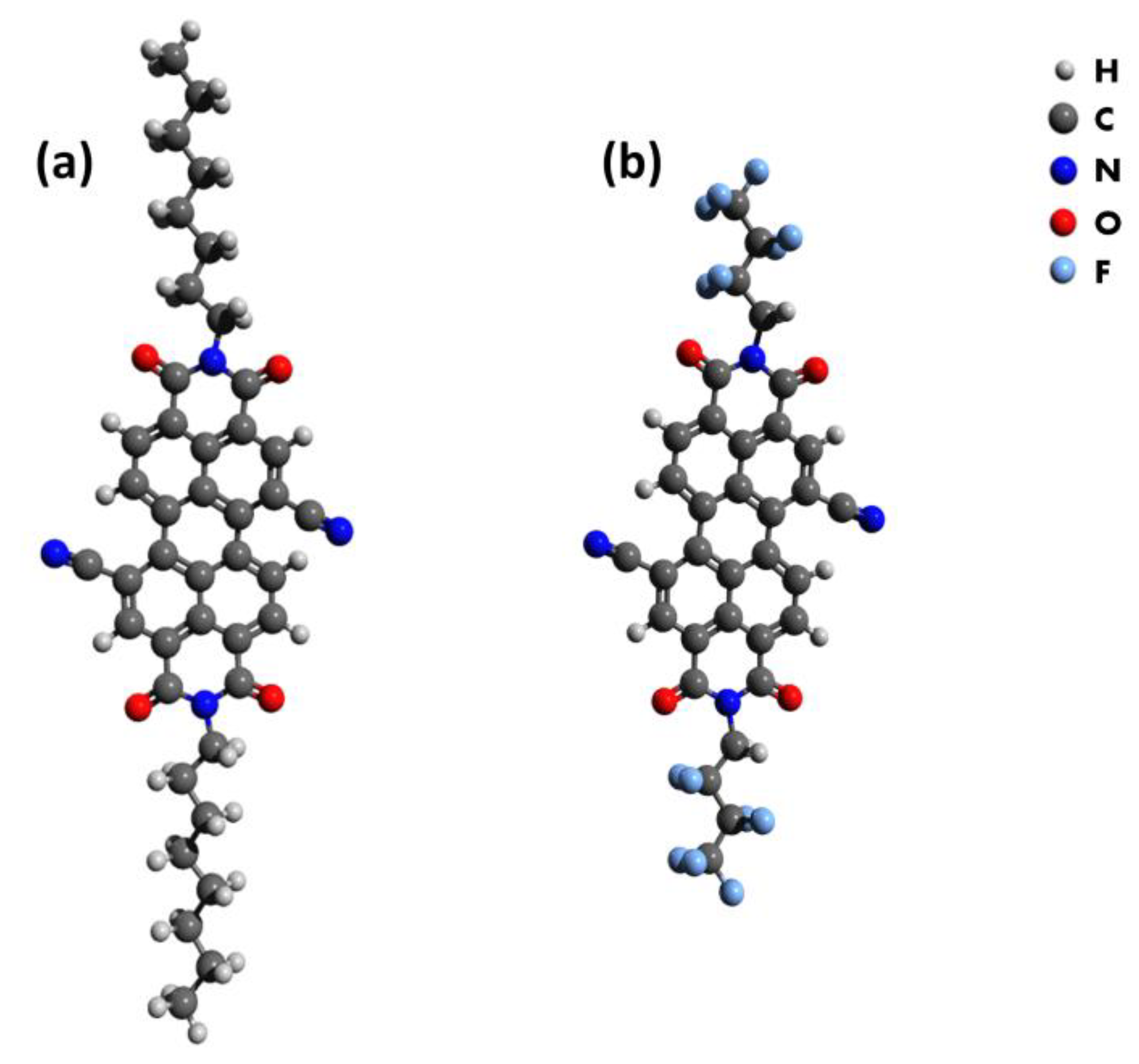
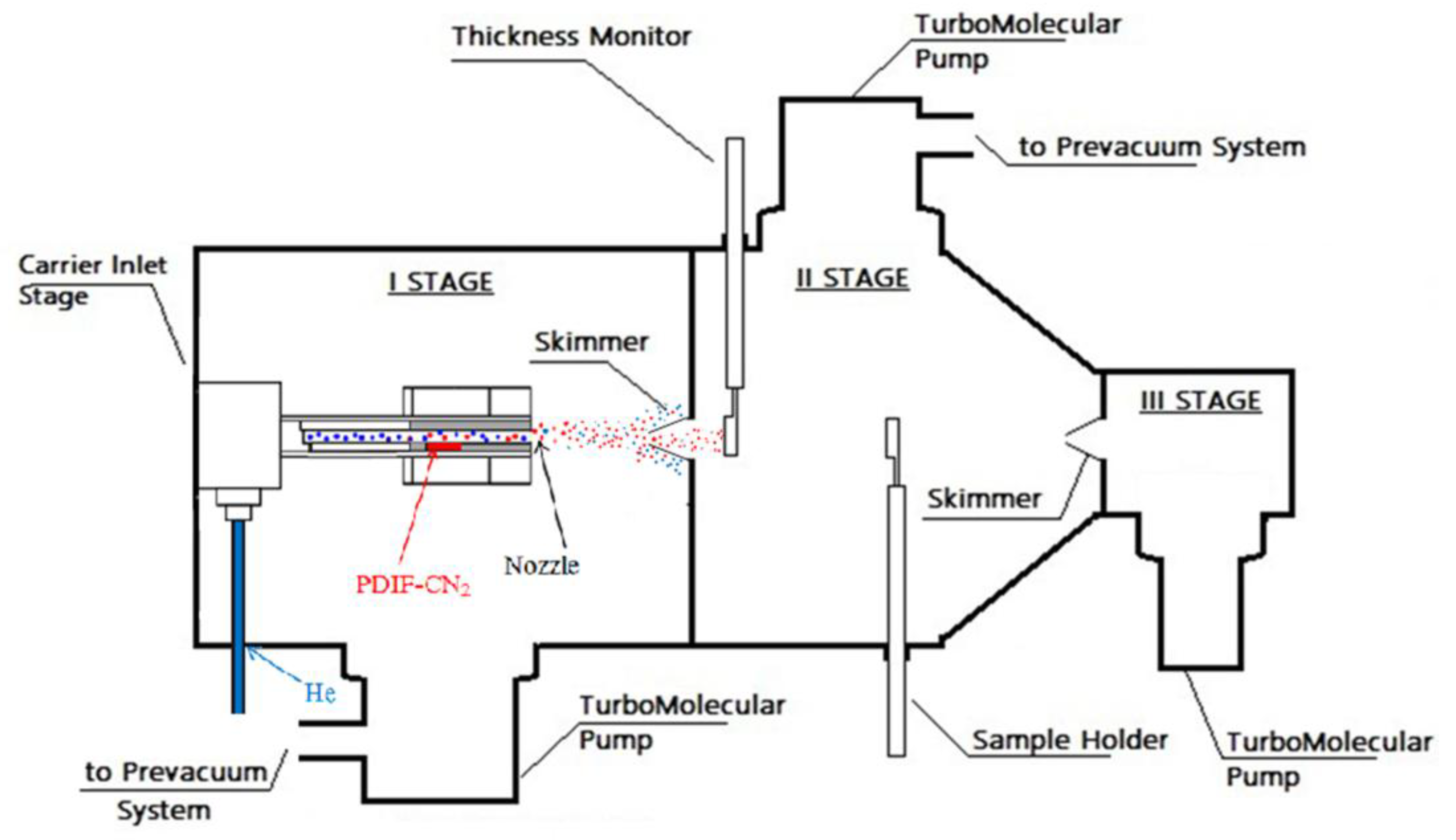
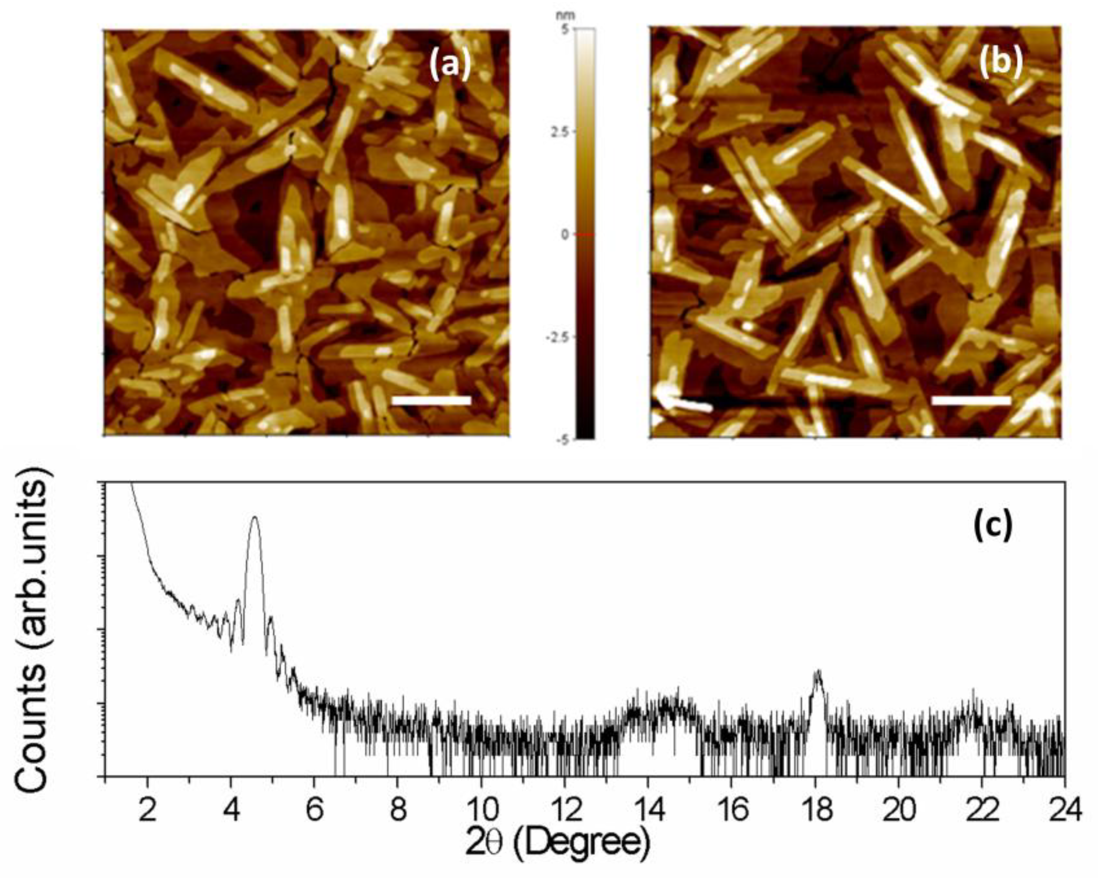
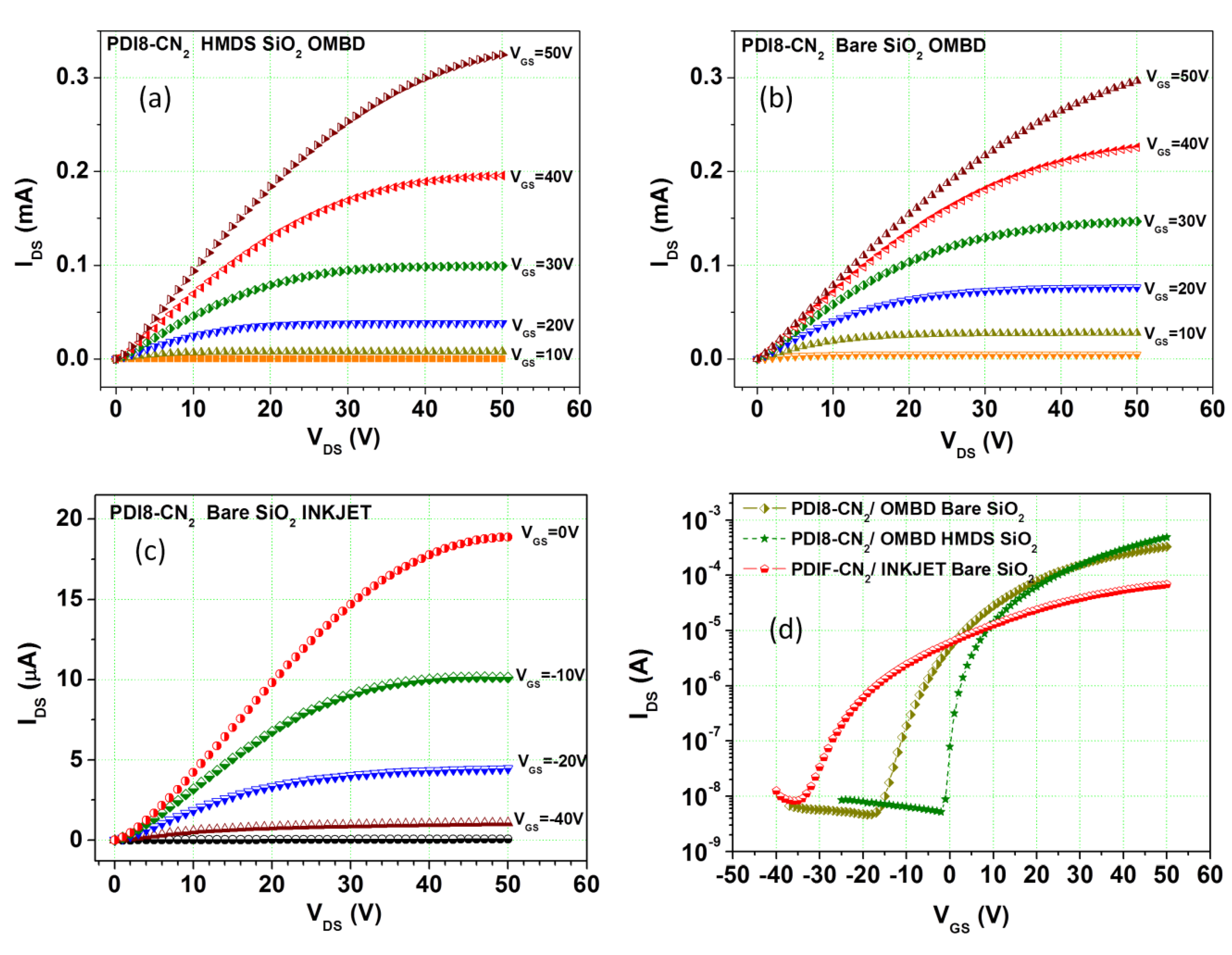
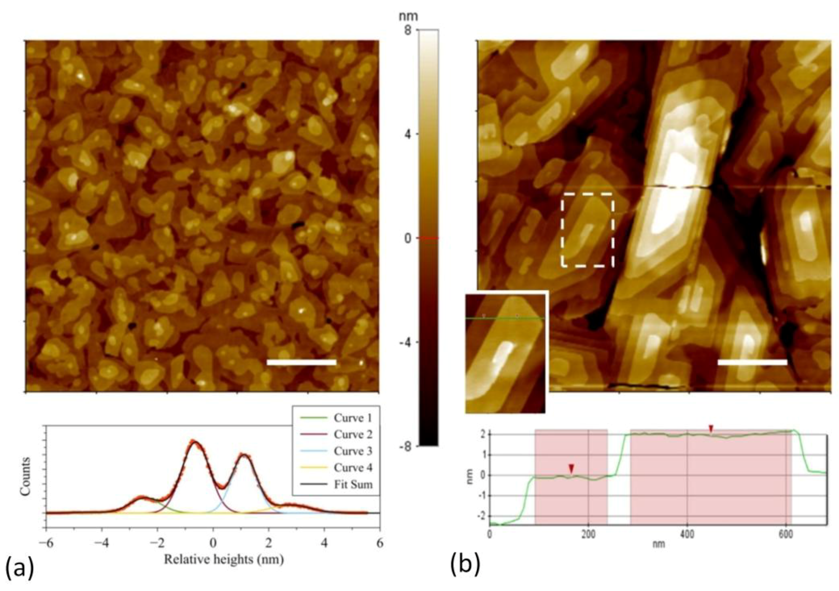
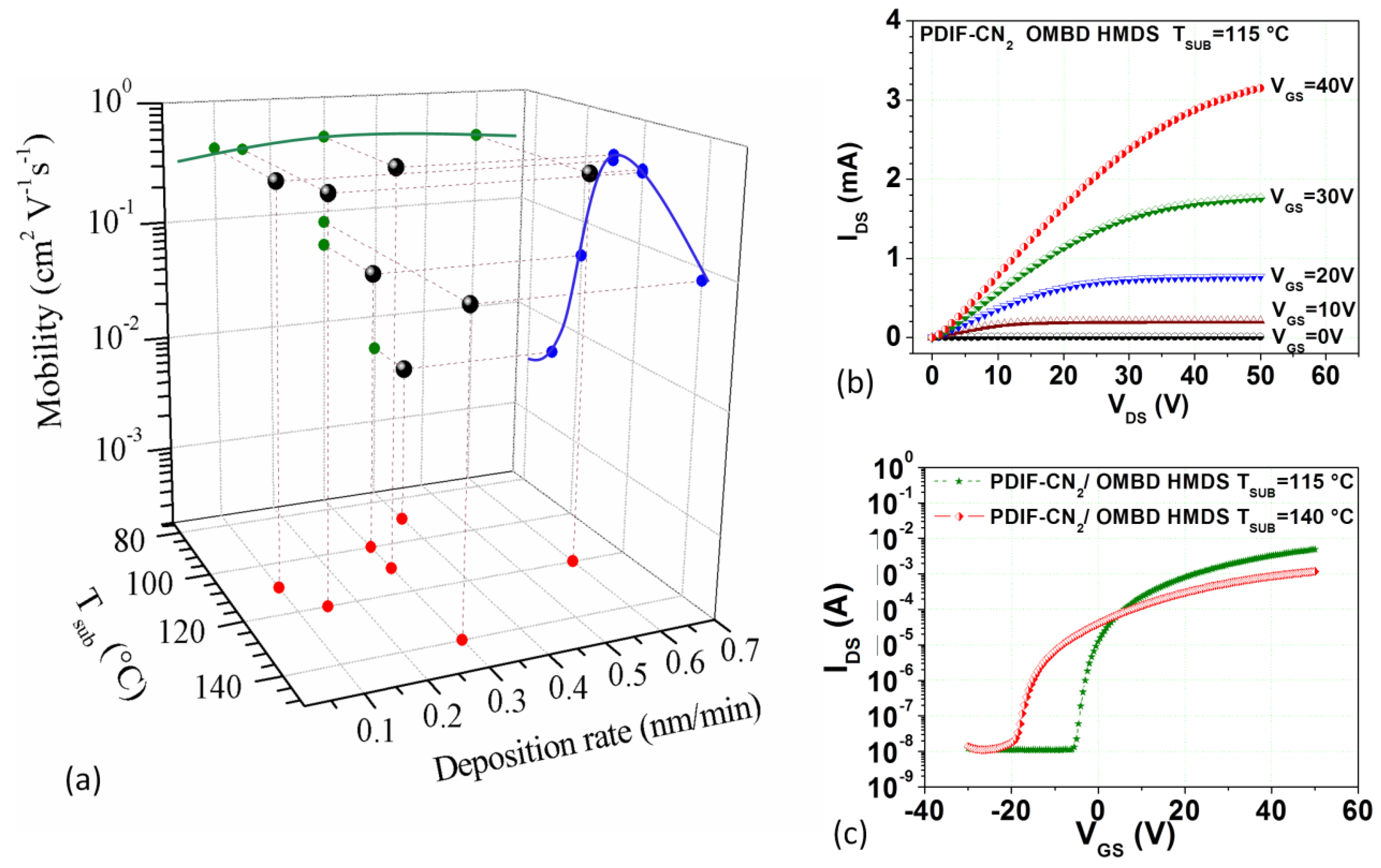
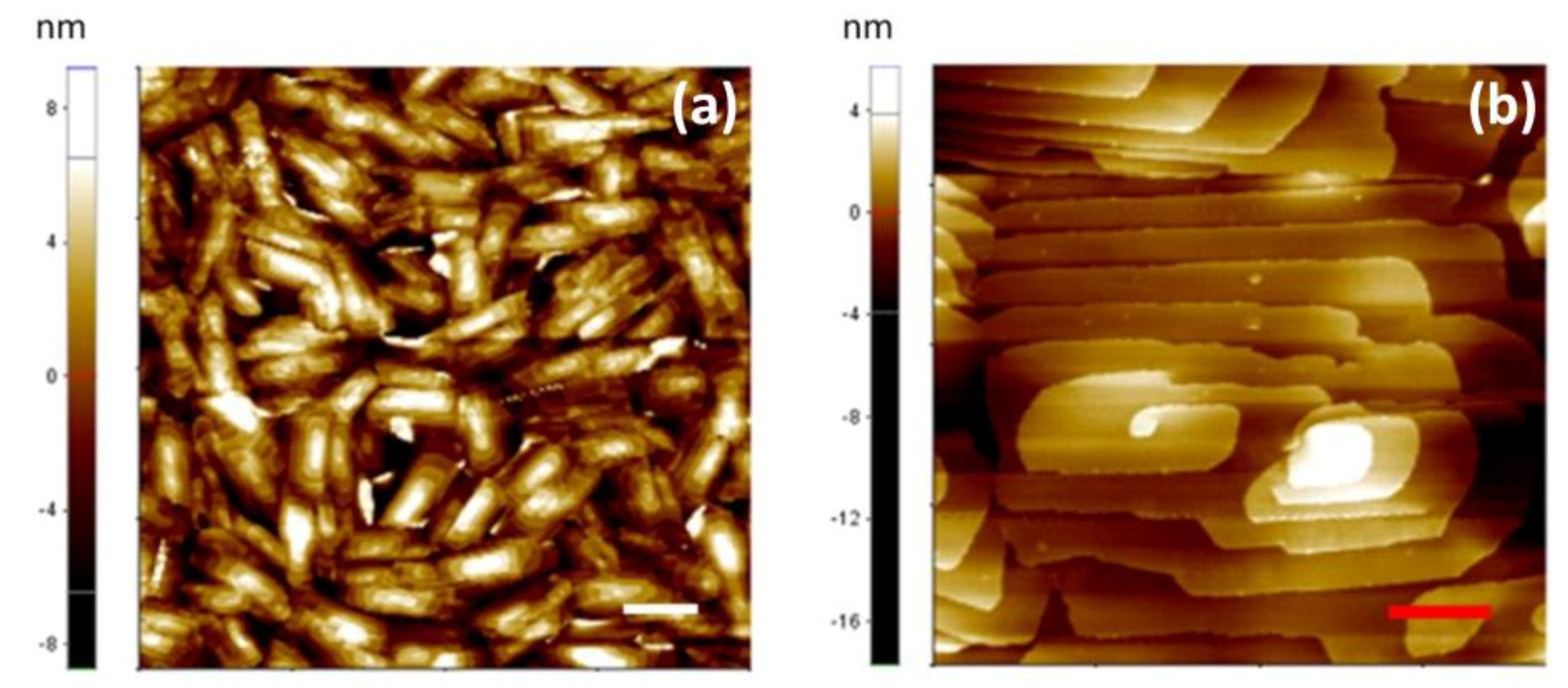
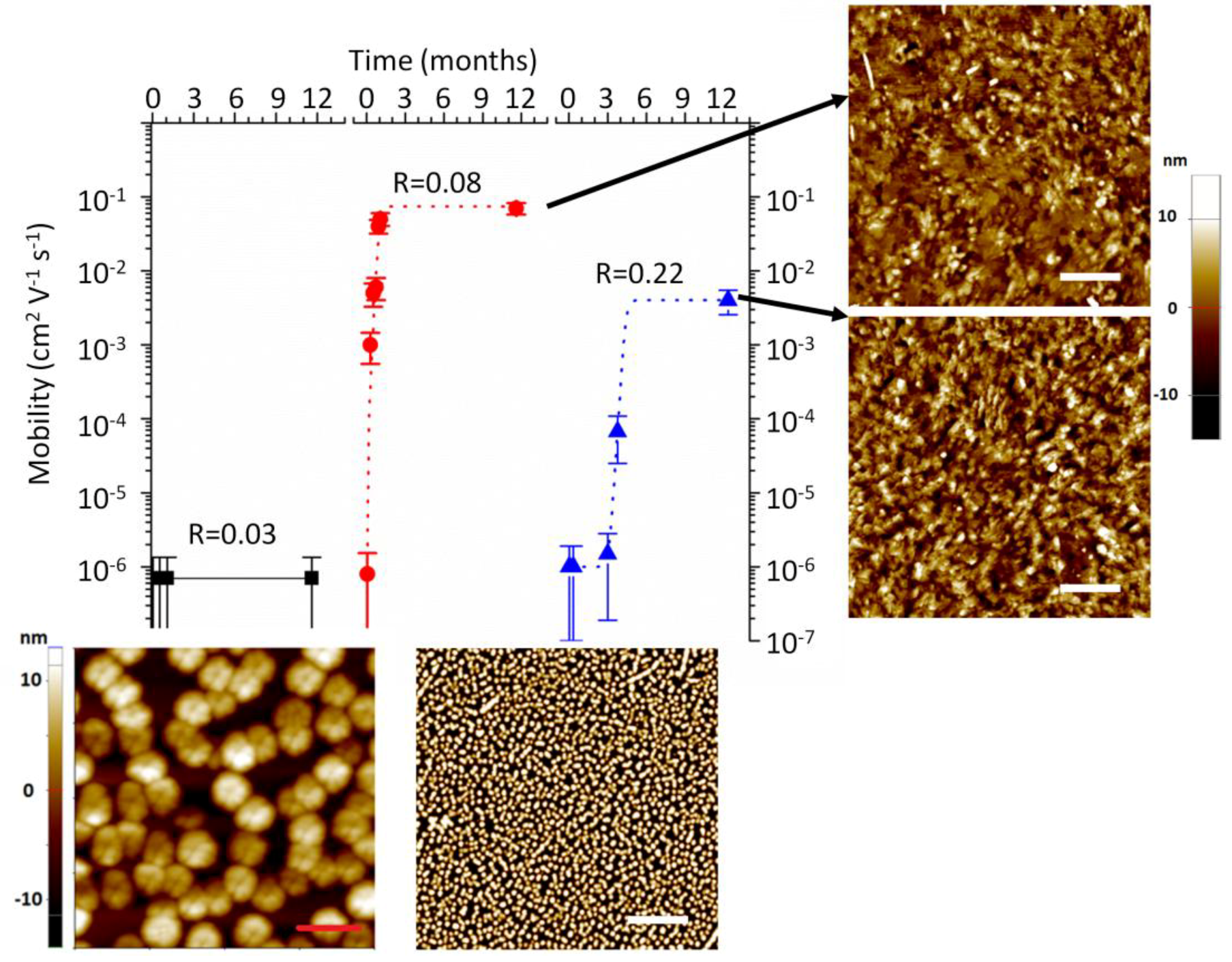
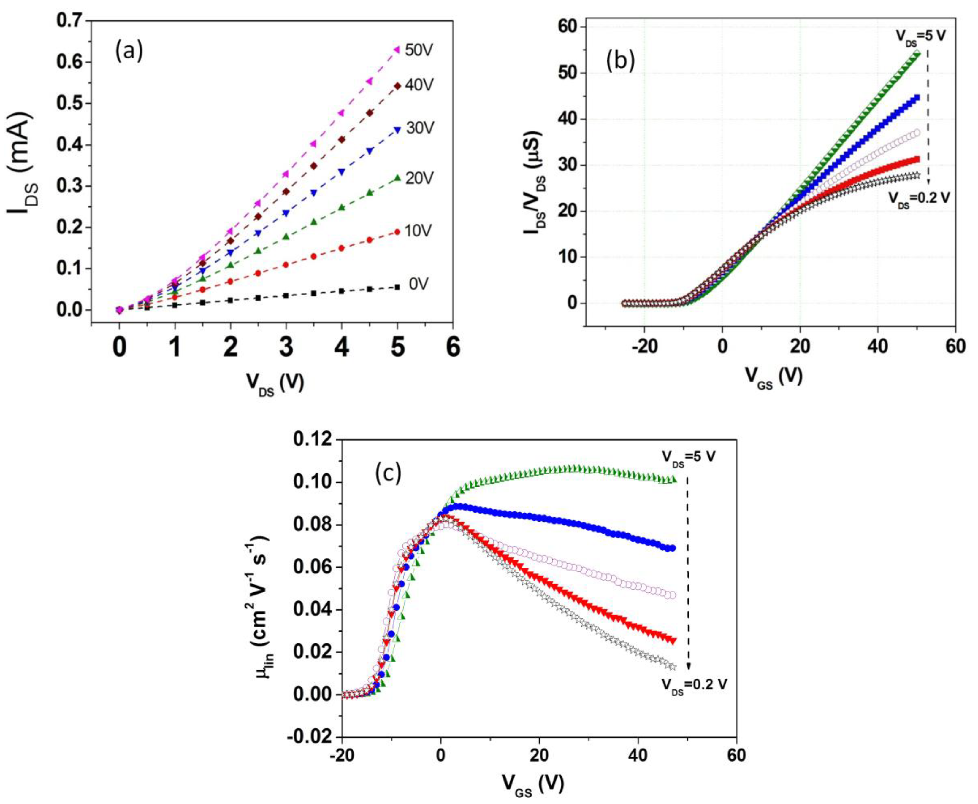
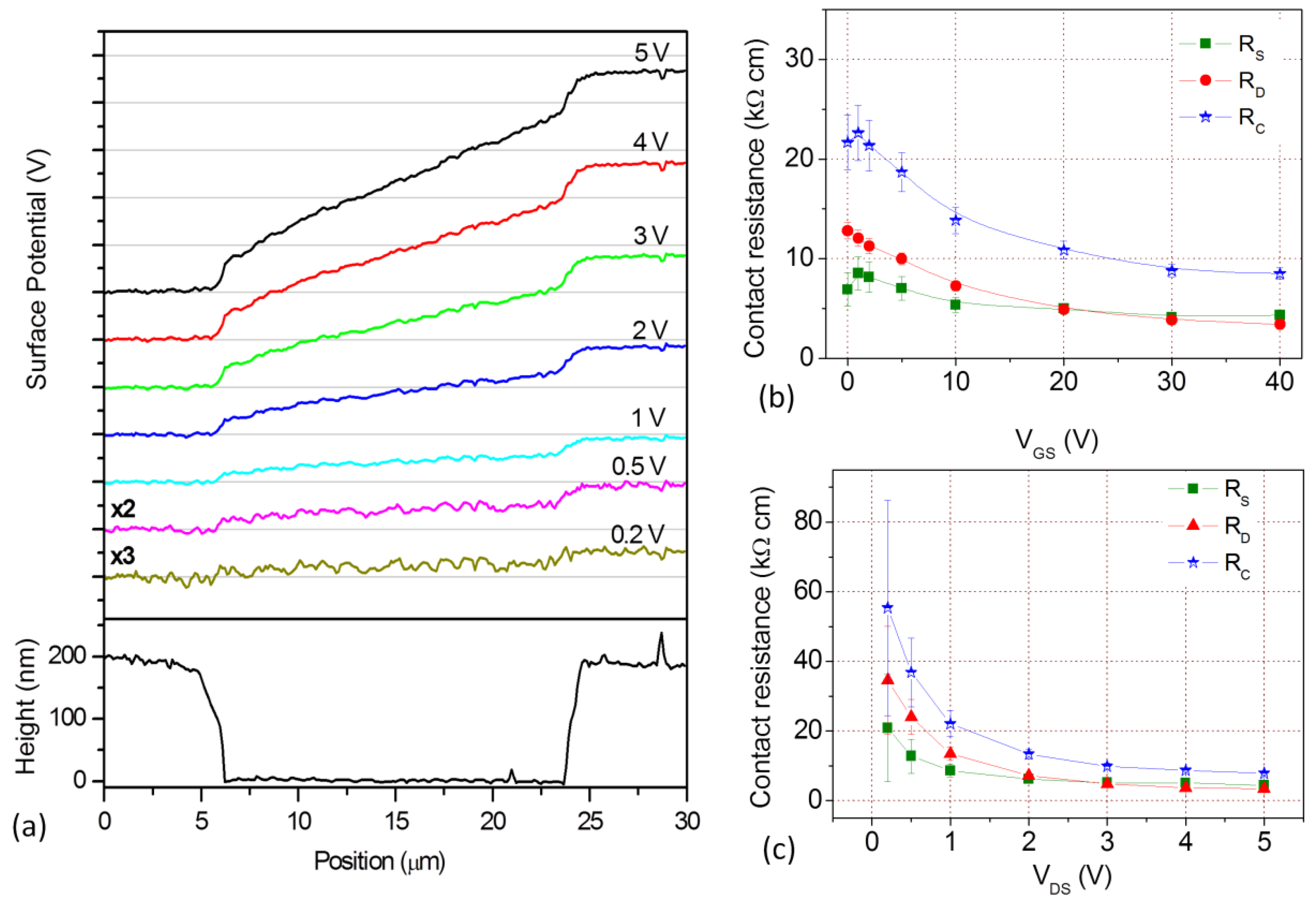
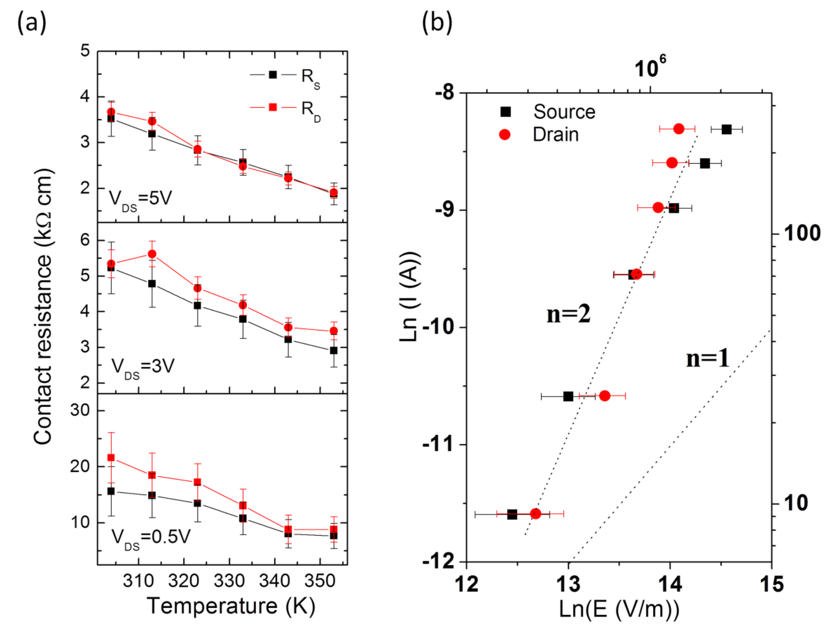
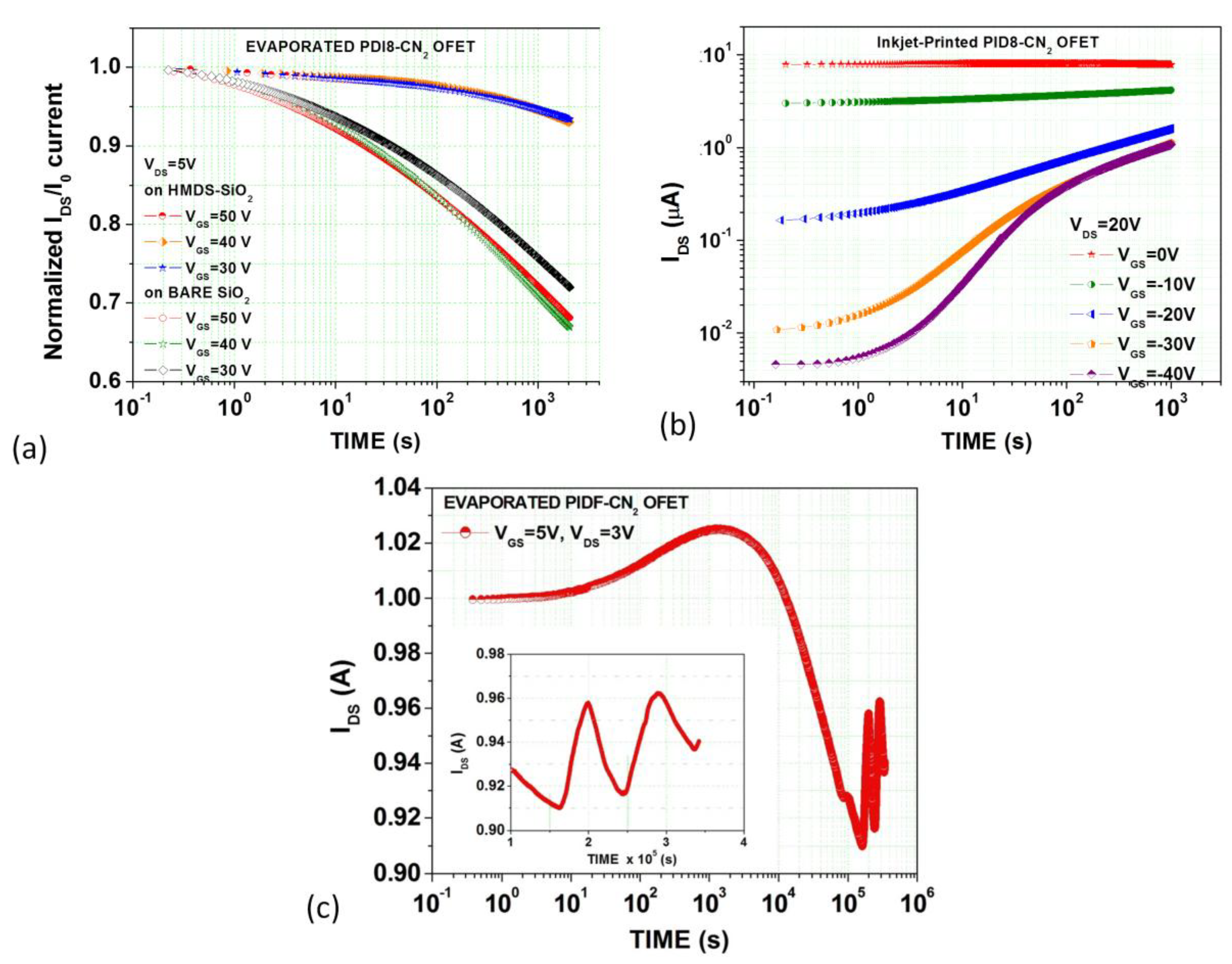
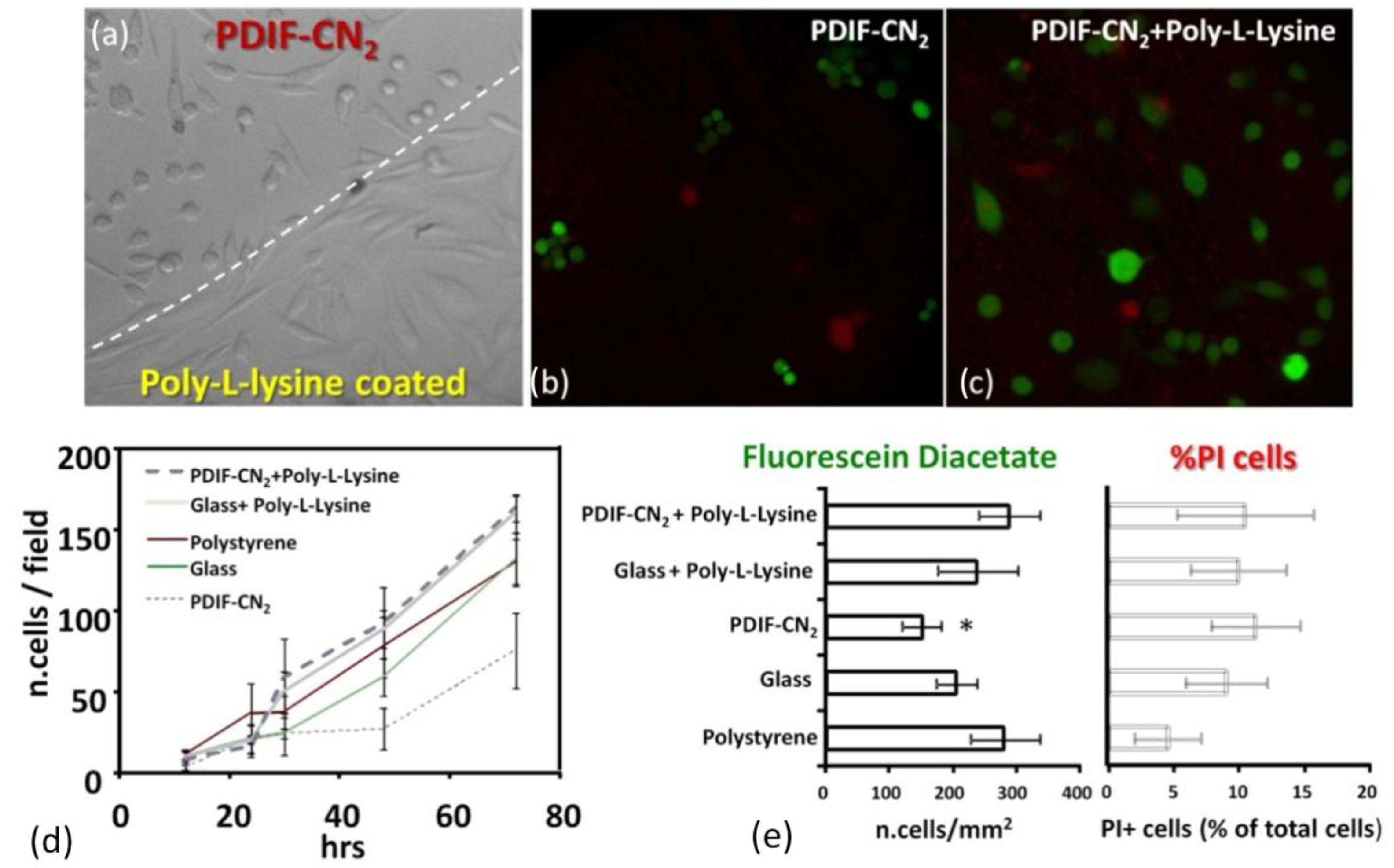
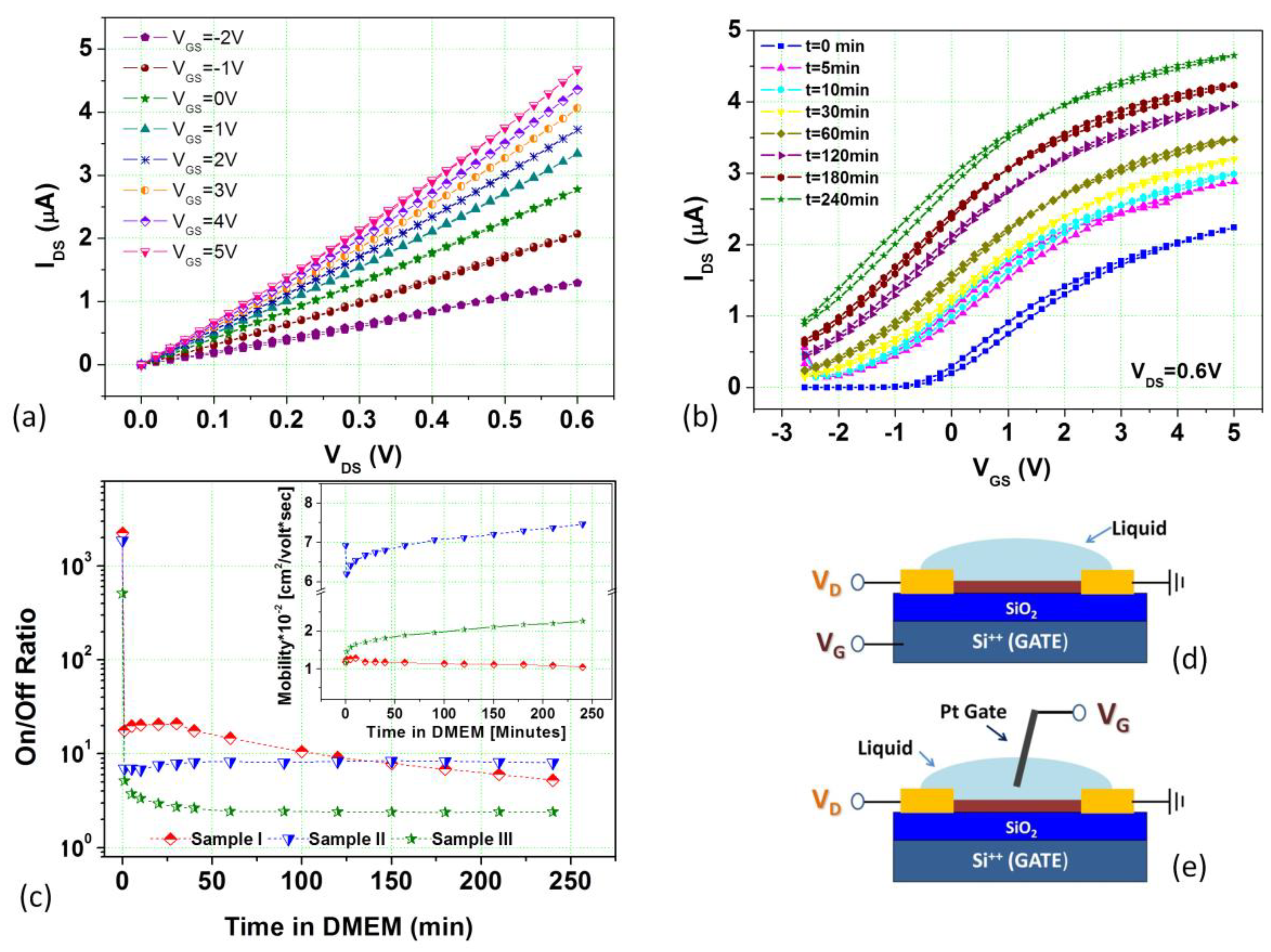
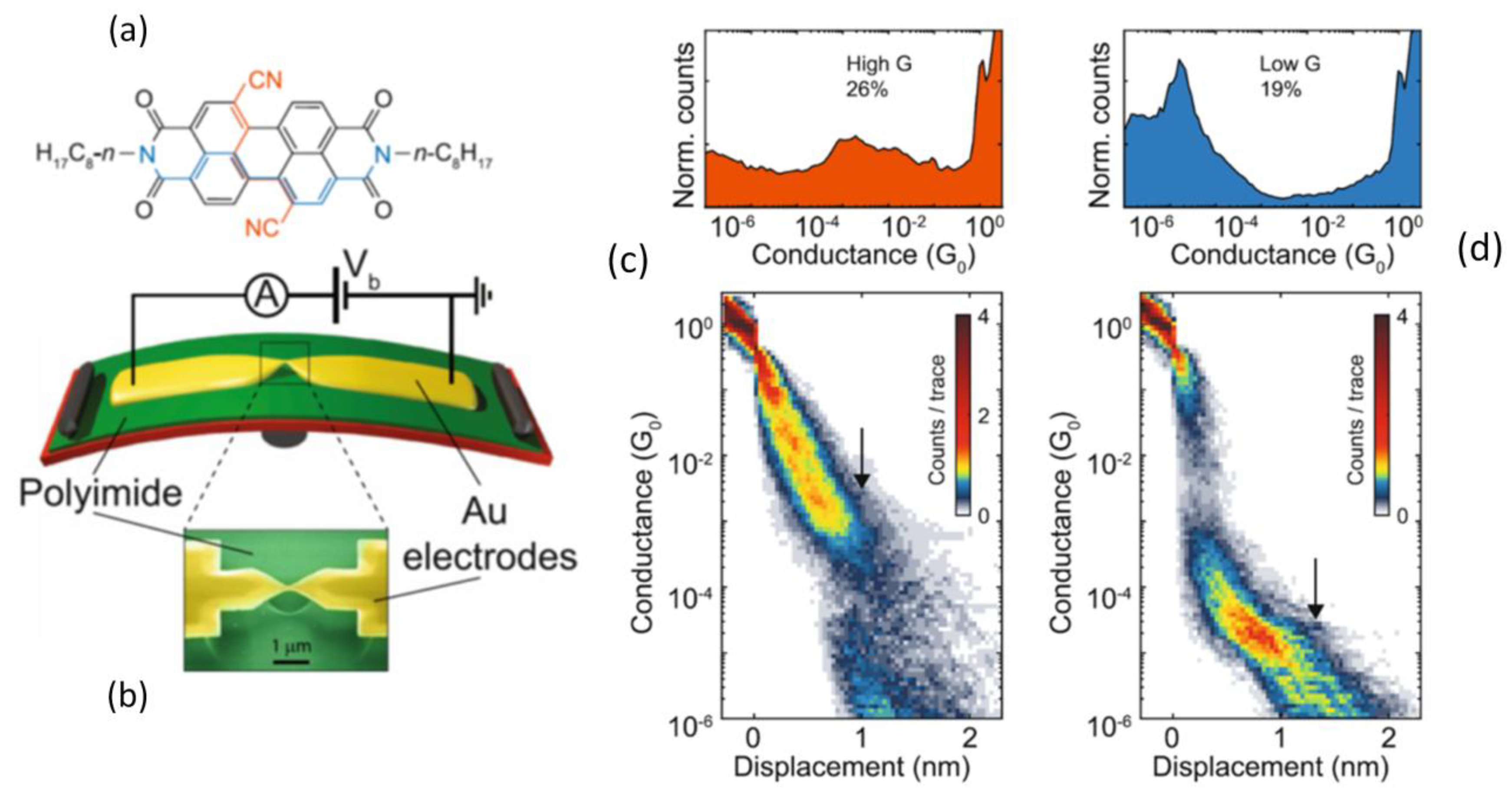
List of Abbreviations.
| Abbreviation | Full Name |
|---|---|
| PDI | Perylene diimide |
| PDI-CY | Core-cyanated perylene diimide |
| PDI8-CN2 | N,N′–bis(n-octyl)-1,6-dicyanoperylene-3,4:9,10-bis(dicarboximide) |
| PDIF-CN2 | N,N′-1H,1H-perfluorobutyl-1,6-dicyanoperylene-3,4:9,10-bis(dicarboximide) |
| LUMO | Lowest unoccupied molecular orbital |
| HOMO | Highest occupied molecular orbital |
| OMBD | Organic molecular bam deposition |
| SuMBD | Supersonic molecular beam deposition |
| AFM | Atomic force microscopy |
| SKPM | Scanning Kelvin probe microscopy |
| TLM | Transmission line method |
| MOSFET | Metal-oxide-semiconductor field-effect transistor |
| OFET | Organic field-effect transistor |
| SCLC | Space charge limited current |
| EBL | Electron beam lithography |
| DCB | O-dichlorobenzene |
| CF | Chloroform |
| PEN | Polyethylene-naphtalate |
| HMDS | Hexamethyldisilazane |
| BS | Bias stress |
| CytopTM | poly(perfluorobutenylvinylether) |
| PI | Propidium iodide |
| CHO | Chinese hamster ovary |
| FDA | Fluorescein diacetate |
| DMEM | Dulbecco modified Eagle’s medium |
| YBCO | YBa2Cu3O7 |
References
- Klauk, H.; Zschieschang, U.; Pflaum, J.; Halik, M. Ultralow-power organic complementary circuits. Nature 2007, 445, 745–748. [Google Scholar] [CrossRef] [PubMed]
- Sundar, V.C.; Zaumseil, J.; Podzorov, V.; Menard, E.; Willett, R.L.; Someya, T.; Gershenson, M.E.; Rogers, J.A. Elastomeric Transistor Stamps: Reversible Probing of Charge Transport in Organic Crystals. Science 2004, 303, 1644–1646. [Google Scholar] [CrossRef] [PubMed]
- Halik, M.; Klauk, H.; Zschieschang, U.; Schmid, G.; Dehm, C.; Schütz, M.; Maisch, S.; Effenberger, F.; Brunnbauer, M.; Stellacci, F. Low-voltage organic transistors with an amorphous molecular gate dielectric. Nature 2004, 431, 963–966. [Google Scholar] [CrossRef] [PubMed]
- Dimitrakopoulos, C.D.; Purushothaman, S.; Kymissis, J.; Callegari, A.; Shaw, J.M. Low-Voltage Organic Transistors on Plastic Comprising High-Dielectric Constant Gate Insulators. Science 1999, 283, 822–824. [Google Scholar] [CrossRef] [PubMed]
- Newman, C.R.; Frisbie, C.D.; da Silva Filho, D.A.; Brèdas, J.L.; Ewbank, P.C.; Mann, K.R. Introduction to Organic Thin Film Transistors and Design of n-Channel Organic Semiconductors. Chem. Mater. 2004, 16, 4436–4451. [Google Scholar] [CrossRef] [Green Version]
- Dimitrakoupoulos, C.D.; Mascaro, D.J. Organic thin-film transistors: A review of recent advances. IBM J. Res. Dev. 2001, 45, 11–27. [Google Scholar] [CrossRef]
- Paterson, A.F.; Singh, S.; Fallon, K.J.; Hodsden, T.; Han, Y.; Schroeder, B.C.; Bronstein, H.; Heeney, M.; McCulloch, I.; Anthopoulos, T.D. Recent Progress in High-Mobility Organic Transistors: A Reality Check. Adv. Mater. 2018, 30, 1801079. [Google Scholar] [CrossRef] [PubMed]
- Choi, H.H.; Cho, K.; Frisbie, D.C.; Sirringhaus, H.; Podzorov, V. Critical assessment of charge mobility extraction in FETs. Nat. Mater. 2018, 17, 2–7. [Google Scholar] [CrossRef]
- Facchetti, A. Semiconductors for organic transistors. Mater. Today 2007, 10, 28–37. [Google Scholar] [CrossRef]
- Chua, L.L.; Zaumseil, J.; Chang, J.F.; Ou, E.C.W.; Ho, P.K.H.; Sirringhaus, H.; Friend, R.H. General observation of n-type field-effect behaviour in organic semiconductors. Nature 2005, 434, 194–199. [Google Scholar] [CrossRef]
- Wurthner, F.; Stolte, M. Naphthalene and perylene diimides for organic transistors. Chem. Commun. 2011, 47, 5109–5115. [Google Scholar] [CrossRef] [PubMed]
- Jones, B.A.; Facchetti, A.; Marks, T.J.; Wasielewski, M.R. Cyanonaphthalene Diimide Semiconductors for Air-Stable, Flexible, and Optically Transparent n-Channel Field-Effect Transistors. Chem. Mater. 2007, 19, 2703–2705. [Google Scholar] [CrossRef]
- Jones, B.A.; Facchetti, A.; Wasielewski, M.R.; Marks, T.J. Tuning Orbital Energetics in Arylene Diimide Semiconductors. Materials Design for Ambient Stability of n-Type Charge Transport. J. Am. Chem. Soc. 2007, 129, 15259–15278. [Google Scholar] [CrossRef] [PubMed]
- Jones, B.A.; Facchetti, A.; Wasielewski, M.R.; Marks, T.J. Effects of Arylene Diimide Thin Film Growth Conditions on n-Channel OFET Performance. Adv. Funct. Mater. 2008, 18, 1329–1339. [Google Scholar] [CrossRef]
- Jung, T.; Yoo, B.; Wang, L.; Dodabalapur, A.; Jones, B.A.; Facchetti, A.; Wasielewski, M.R.; Marks, T.J. Nanoscale n-channel and ambipolar organic field-effect transistors. Appl. Phys. Lett. 2006, 88, 183102. [Google Scholar] [CrossRef]
- Jones, B.A.; Ahrens, M.J.; Yoon, M.H.; Facchetti, A.; Marks, T.J.; Wasielewski, M.R. High-Mobility Air-Stable n-Type Semiconductors with Processing Versatility: Dicyanoperylene-3,4:9,10-bis(dicarboximides). Angew. Chem. Int. Ed. 2004, 43, 6363–6366. [Google Scholar] [CrossRef] [PubMed]
- Schmidt, R.; Oh, J.H.; Sun, Y.S.; Deppisch, M.; Krause, A.M.; Radacki, K.; Braunschweig, H.; Könemann, M.; Erk, P.; Bao, Z.; et al. High-Performance Air-Stable n-Channel Organic Thin Film Transistors Based on Halogenated Perylene Bisimide Semiconductors. J. Am. Chem. Soc. 2009, 131, 6215–6228. [Google Scholar] [CrossRef]
- Ling, M.M.; Erk, P.; Gomez, M.; Koenemann, M.; Locklin, J.; Bao, Z. Air-Stable n-Channel Organic Semiconductors Based on Perylene Diimide Derivatives without Strong Electron Withdrawing Groups. Adv. Mater. 2007, 19, 1123–1127. [Google Scholar] [CrossRef]
- Schmidt, R.; Ling, M.M.; Oh, J.H.; Winkler, M.; Könemann, M.; Bao, Z.; Würthner, F. Core-Fluorinated Perylene Bisimide Dyes: Air Stable n-Channel Organic Semiconductors for Thin Film Transistors with Exceptionally High On-to-Off Current Ratios. Adv. Mater. 2007, 19, 3692–3695. [Google Scholar] [CrossRef]
- Horowitz, G.; Kouki, F.; Spearman, P.; Fichou, D.; Nogues, C.; Pan, X.; Garnier, F. Evidence for n-type conduction in a perylene tetracarboxylic diimide derivative. Adv. Mater. 1996, 8, 242–245. [Google Scholar] [CrossRef]
- Malenfant, P.R.L.; Dimitrakopoulos, C.D.; Gelorme, J.D.; Kosbar, L.L.; Graham, T.O.; Curioni, A.; Andreoni, W. N-type organic thin-film transistor with high field-effect mobility based on a N,N′-dialkyl-3,4,9,10-perylene tetracarboxylic diimide derivative. Appl. Phys. Lett. 2002, 80, 2517. [Google Scholar] [CrossRef]
- Chesterfield, R.J.; McKeen, J.C.; Newman, C.R.; Frisbie, C.D.; Ewbank, P.C.; Mann, K.R.; Miller, L.L. Variable temperature film and contact resistance measurements on operating n-channel organic thin film transistors. Appl. Phys. Lett. 2004, 95, 6396. [Google Scholar]
- Chesterfield, R.J.; McKeen, J.C.; Newman, C.R.; Ewbank, P.C.; da Silva Filho, D.A.; Brèdas, J.L.; Miller, L.L.; Mann, K.R.; Frisbie, C.D. Organic Thin Film Transistors Based on N-Alkyl Perylene Diimides: Charge Transport Kinetics as a Function of Gate Voltage and Temperature. J. Phys. Chem. B 2004, 108, 19281–19292. [Google Scholar] [CrossRef]
- Tatemichi, S.; Ichikawa, M.; Koyama, T.; Taniguchi, Y. High mobility n-type thin-film transistors based on N,N′-ditridecyl perylene diimide with thermal treatments. Appl. Phys. Lett. 2006, 89, 112108. [Google Scholar] [CrossRef]
- Weitz, R.T.; Amsharov, K.; Zschieschang, U.; Barrena Villas, E.; Goswami, D.K.; Burghard, M.; Dosch, H.; Jansen, M.; Kern, K.; Klauk, H. Organic n-Channel Transistors Based on Core-Cyanated Perylene Carboxylic Diimide Derivatives. J. Am. Chem. Soc. 2008, 130, 4637–4645. [Google Scholar] [CrossRef] [PubMed]
- Kraft, U.; Sejfic, M.; Kang, M.J.; Takimiya, K.; Zaki, T.; Letzkus, F.; Burghartz, J.N.; Weber, E.; Klauk, H. Flexible low-voltage organic complementary circuits: Finding the optimum combination of semiconductors and monolayer gate dielectrics. Adv. Mater. 2015, 27, 207–214. [Google Scholar] [CrossRef] [PubMed]
- Molinari, A.S.; Alves, H.; Chen, Z.; Facchetti, A.; Morpurgo, A.F. High Electron Mobility in Vacuum and Ambient for PDIF-CN2 Single-Crystal Transistors. J. Am. Chem. Soc. 2009, 131, 2462–2463. [Google Scholar] [CrossRef] [PubMed]
- Yi, H.T.; Chen, Z.; Facchetti, A.; Podzorov, V. Solution-Processed Crystalline n-Type Organic Transistors Stable against Electrical Stress and Photooxidation. Adv. Funct. Mater. 2016, 26, 2365–2370. [Google Scholar] [CrossRef]
- Willa, K.; Häusermann, R.; Mathis, T.; Facchetti, A.; Chen, Z.; Batlogg, B. From organic single crystals to solution processed thin-films: Charge transport and trapping with varying degree of order. J. Appl. Phys. 2013, 113, 133707. [Google Scholar] [CrossRef]
- Minder, N.A.; Ono, S.; Chen, Z.; Facchetti, A.; Morpurgo, A.F. Band-Like Electron Transport in Organic Transistors and Implication of the Molecular Structure for Performance Optimization. Adv. Mater. 2012, 24, 503–508. [Google Scholar] [CrossRef]
- Barra, M.; Di Girolamo, F.V.; Minder, N.A.; Gutierrez Lezama, I.; Chen, Z.; Facchetti, A.; Morpurgo, A.F.; Cassinese, A. Very low bias stress in n-type organic single crystal transistors. Appl. Phys. Lett. 2012, 100, 133301. [Google Scholar] [CrossRef]
- Gao, X.; Hu, Y. Development of n-type organic semiconductors for thin film transistors: A viewpoint of molecular design. J. Mater. Chem. C 2014, 2, 3099. [Google Scholar] [CrossRef]
- Quinn, J.T.E.; Zhu, J.; Xu, L.; Wang, J.; Li, Y. Recent progress in the development of n-type organic semiconductors for organic field effect transistors. J. Mater. Chem. C 2017, 5, 8654. [Google Scholar] [CrossRef]
- Forrest, S.R. The path to ubiquitous and low-cost organic electronic appliances on plastic. Nature 2004, 428, 911–918. [Google Scholar] [CrossRef] [PubMed]
- Riccio, M.; Irace, A.; Breglio, G.; Rossi, L.; Barra, M.; Di Girolamo, F.V.; Cassinese, A. Current distribution effects in organic sexithiophene FETs investigated by lock-in thermography: mobility evaluation issues. Appl. Phys. Lett. 2008, 93, 243504. [Google Scholar]
- Iannotta, S.; Toccoli, T. Supersonic molecular beam growth of thin films of organic materials: A novel approach to controlling the structure, morphology, and functional properties. J. Polym. Sci. Part B Polym. Phys. 2003, 41, 2501–2521. [Google Scholar]
- Wu, Y.; Toccoli, T.; Koch, N.; Iacob, E.; Pallaoro, A.; Rudolf, P.; Iannotta, S. Controlling the Early Stages of Pentacene Growth by Supersonic Molecular Beam Deposition. Phys. Rev. Lett. 2007, 98, 076601. [Google Scholar] [CrossRef] [PubMed] [Green Version]
- Benvenuti, E.; Gentili, D.; Chiarella, F.; Portone, A.; Barra, M.; Cecchini, M.; Cappuccino, C.; Zambianchi, M.; Lopez, S.G.; Salzillo, T.; et al. Tuning polymorphism in 2,3-thienoimide capped oligothiophene based field-effect transistors by implementing vacuum and solution deposition methods. J. Mater. Chem. C 2018, 6, 5601–5608. [Google Scholar] [CrossRef]
- Chiarella, F.; Chianese, F.; Barra, M.; Parlato, L.; Toccoli, T.; Cassinese, A. Spontaneous Wetting Dynamics in Perylene Diimide n-Type Thin Films Deposited at Room Temperature by Supersonic Molecular Beam. J. Phys. Chem. C 2016, 120, 26076–26082. [Google Scholar] [CrossRef]
- Bloisi, F.; Pezzella, A.; Barra, M.; Alfè, M.; Chiarella, F.; Cassinese, A.; Vicari, L. Effect of substrate temperature on MAPLE deposition of synthetic eumelanin films. Appl. Phys. A 2011, 105, 619–627. [Google Scholar] [CrossRef]
- Barra, M.; Viggiano, D.; Ambrosino, P.; Bloisi, F.; Di Girolamo, F.V.; Soldovieri, M.V.; Taglialatela, M.; Cassinese, A. Addressing the use of PDIF-CN2 molecules in the development of n-type organic field-effect transistors for biosensing applications. Biochim. Biophys. Acta 2013, 1830, 4365–4373. [Google Scholar] [CrossRef]
- Liscio, F.; Milita, S.; Albonetti, C.; D’Angelo, P.; Guagliardi, A.; Masciocchi, N.; Della Valle, R.G.; Venuti, E.; Brillante, A.; Biscarini, F. Structure and Morphology of PDI8-CN2 for N-Type Thin-Film Transistor. Adv. Funct. Mater. 2012, 22, 943–953. [Google Scholar] [CrossRef]
- Liscio, F.; Albonetti, C.; Broch, K.; Shehu, A.; Quiroga, S.D.; Ferlauto, L.; Frank, C.; Kowarik, S.; Nervo, R.; Gerlach, A.; et al. Molecular Reorganization in Organic Field-Effect Transistors and Its Effect on Two-Dimensional Charge Transport Pathways. ACS Nano 2013, 7, 1257–1264. [Google Scholar] [CrossRef] [PubMed]
- Barra, M.; Di Girolamo, F.V.; Chiarella, F.; Salluzzo, M.; Chen, Z.; Facchetti, A.; Anderson, L.; Cassinese, A. Transport Property and Charge Trap Comparison for N-Channel Perylene Diimide Transistors with Different Air-Stability. J. Phys. Chem. C 2010, 114, 20387–20393. [Google Scholar] [CrossRef]
- Di Girolamo, F.V.; Ciccullo, F.; Barra, M.; Carella, A.; Cassinese, A. Investigation on bias stress effects in n-type PDI8-CN2 thin-film transistors. Org. Electron. 2012, 13, 2281–2289. [Google Scholar] [CrossRef]
- Chiarella, F.; Barra, M.; Cassinese, A.; Di Girolamo, F.V.; Maddalena, P.; Santamaria, L.; Lettieri, S. Dicyanoperylene-diimide thin-film growth: A combined optical and morphological study. Appl. Phys. A 2011, 104, 39–46. [Google Scholar] [CrossRef]
- Buzio, R.; Gerbi, A.; Barra, M.; Chiarella, F.; Gnecco, E.; Cassinese, A. Subnanometer resolution and Enhanced Friction Contrast at the Surface of Perylene Diimide PDI8-CN2 Thin Films in Ambient Conditions. Langmuir 2018, 34, 3207–3214. [Google Scholar] [CrossRef] [PubMed]
- Bobbert, P.A.; Sharma, A.; Mathijssen, S.G.J.; Kemerink, M.; De Leeuw, D.M. Operational stability of organic field-effect transistors. Adv. Mater. 2012, 24, 1146–1158. [Google Scholar] [CrossRef]
- Grimaldi, I.A.; Barra, M.; De Girolamo Del Mauro, A.; Loffredo, F.; Cassinese, A.; Villani, F.; Minarini, C. Inkjet printed perylene diimide based OTFTs: Effect of the solvent mixture and the printing parameters on film morphology. Synth. Met. 2012, 161, 2618–2622. [Google Scholar] [CrossRef]
- Piliego, C.; Jarzab, D.; Gigli, G.; Chen, Z.; Facchetti, A.; Loi, M.A. High Electron Mobility and Ambient Stability in Solution-Processed Perylene-Based Organic Field-Effect Transistors. Adv. Mater. 2009, 21, 1573–1576. [Google Scholar] [CrossRef]
- Yoo, B.; Jones, B.A.; Basu, D.; Fine, D.; Jung, T.; Mohapatra, S.; Facchetti, A.; Dimmler, K.; Wasielewski, M.R.; Marks, T.J.; et al. High-Performance Solution-Deposited n-Channel Organic Transistors and their Complementary Circuits. Adv. Mater. 2007, 19, 4028–4032. [Google Scholar] [CrossRef]
- Chiarella, F.; Barra, M.; Ricciotti, L.; Aloisio, A.; Cassinese, A. Morphology, Electrical Performance and Potentiometry of PDIF-CN2 Thin-Film Transistors on HMDS-Treated and Bare Silicon Dioxide. Electronics 2014, 3, 76–86. [Google Scholar] [CrossRef]
- Belova, V.; Wagner, B.; Reisz, B.; Zeiser, C.; Duva, G.; Rozboril, J.; Novak, J.; Gerlach, A.; Hinderhofer, A.; Schreiber, F. Real-Time Structural and Optical Study of Growth and Packing Behavior of Perylene Diimide Derivative Thin Films: Influence of Side-Chain Modification. J. Phys. Chem. C 2018, 122, 8589–8601. [Google Scholar] [CrossRef]
- Rapisarda, M.; Calvi, S.; Barra, M.; Chiarella, F.; Di Capua, F.; Cassinese, A.; Aloisio, A.; Mariucci, L. Staggered top-gate PDIF-CN2 N-type thin film transistors on flexible plastic substrates. Org. Electron. 2018, 57, 226–231. [Google Scholar] [CrossRef]
- Casalis, L.; Danisman, M.F.; Nickel, B.; Bracco, G.; Toccoli, T.; Iannotta, S.; Scoles, G. Hyperthermal Molecular Beam Deposition of Highly Ordered Organic Thin Films. Phys. Rev. Lett. 2003, 90, 206101. [Google Scholar] [CrossRef] [PubMed]
- Chiarella, F.; Toccoli, T.; Barra, M.; Aversa, L.; Ciccullo, F.; Tatti, R.; Verucchi, R.; Iannotta, S.; Cassinese, A. High mobility n-type organic thin-film transistors deposited at room temperature by supersonic molecular beam deposition. Appl. Phys. Lett. 2014, 104, 143302. [Google Scholar] [CrossRef]
- Chiarella, F.; Perroni, C.A.; Chianese, F.; Barra, M.; De Luca, G.M.; Cataudella, V.; Cassinese, A. Post-Deposition Wetting and Instabilities in Organic Thin Films by Supersonic Molecular Beam Deposition. Sci. Rep. 2018, 8, 12015. [Google Scholar] [CrossRef] [PubMed]
- Liu, C.; Xu, Y.; Noh, Y.Y. Contact engineering in organic field-effect transistors. Mat. Today 2015, 18, 79–96. [Google Scholar] [CrossRef]
- Natali, D.; Caironi, M. Charge injection in solution-processed organic field-effect transistors: Physics, models and characterization methods. Adv. Mater. 2012, 15, 1357–1387. [Google Scholar] [CrossRef]
- Klauk, H. Will We See Gigahertz Organic Transistors? Adv. Electron. Mater. 2018, 4, 1700474. [Google Scholar] [CrossRef]
- Dinelli, F.; Murgia, M.; Levy, P.; Cavallini, M.; Biscarini, F.; de Leeuw, D.M. Spatially correlated charge transport in organic thin film transistors. Phys. Rev. Lett. 2004, 92, 116802. [Google Scholar] [CrossRef]
- Chiarella, F.; Barra, M.; Carella, A.; Parlato, L.; Sarnelli, E.; Cassinese, A. Contact-resistance effects in PDI8-CN2 n-type thin-film transistors investigated by Kelvin-probe potentiometry. Org. Electron. 2016, 28, 299–305. [Google Scholar] [CrossRef]
- Chianese, F.; Chiarella, F.; Barra, M.; Carella, A.; Cassinese, A. Scanning Kelvin Probe Microscopy investigation of the contact resistances and charge mobility in n-type PDIF-CN2 thin-film transistors. Org. Electron. 2018, 52, 206–212. [Google Scholar] [CrossRef]
- Liu, C.; Huseynova, G.; Xu, Y.; Long, D.X.; Park, W.; Liu, X.; Minari, T.; Noh, Y.Y. Universal diffusion-limited injection and the hook effect in organic thin-film transistors. Sci. Rep. 2016, 6, 29811. [Google Scholar] [CrossRef] [PubMed] [Green Version]
- Buzio, R.; Gerbi, A.; Marrè, D.; Barra, M.; Cassinese, A. Electron injection barrier and energy-level alignment at the Au/PDI8-CN2 interface via current–voltage measurements and ballistic emission microscopy. Org. Electron. 2015, 18, 44–52. [Google Scholar] [CrossRef]
- Buzio, R.; Gerbi, A.; Marrè, D.; Barra, M.; Cassinese, A. Ballistic electron and photocurrent transport in Au/organic/Si(001) diodes with PDI8-CN2 interlayers. J. Vac. Sci. Technol. B 2016, 34, 041212. [Google Scholar] [CrossRef]
- Youn, J.; Dholakia, G.R.; Huang, H.; Hennek, J.W.; Facchetti, A.; Marks, T.J. Influence of thiol self-assembled monolayer processing on bottom-contact thin-film transistors based on n-type organic semiconductors. Adv. Funct. Mater. 2012, 22, 1856–1869. [Google Scholar] [CrossRef]
- Rose, A. Space-charge-limited currents in solids. Phys. Rev. 1955, 97, 1538–1544. [Google Scholar] [CrossRef]
- Silveira, W.R.; Marohn, J.A. Microscopic view of charge injection in an organic semiconductor. Phys. Rev. Lett. 2004, 93, 2–5. [Google Scholar] [CrossRef]
- Parlato, L.; Sarnelli, E.; Cassinese, A.; Chianese, F.; Chiarella, F.; Nappi, C.; Barra, M. Improving the electrical performance of PDI8-CN2 bottom-gate coplanar organic thin-film transistors. Appl. Phys. A 2018, 124, 708. [Google Scholar] [CrossRef]
- Congyan, L.; Zhuoyu, J.; Guangwei, X.; Nianduan, L.; Ling, L.; Ming, L. Charge-transfer complex modified bottom electrodes for high performance low voltage organic field-effect transistors and circuits. Org. Electron. 2017, 49, 206–211. [Google Scholar]
- Nomoto, K.; Hirai, N.; Yoneya, N.; Kawashima, N.; Noda, M.; Wada, M.; Kasahara, J. A high-performance short-channel bottom-contact OTFT and its application to AM-TN-LCD. IEEE Trans. Electron. Devices 2005, 52, 1519–1526. [Google Scholar] [CrossRef]
- Sirringhaus, H. Reliability of organic field-effect transistors. Adv. Mater. 2009, 21, 3859. [Google Scholar] [CrossRef]
- Mathijssen, S.G.J.; Colle, M.; Gomes, H.; Smits, E.C.P.; de Boer, B.; McCulloch, P.A.; Bobbert, P.; de Leeuw, D.M. Dynamics of threshold voltage shifts in organic and amorphous silicon field-effect transistors. Adv. Mater. 2007, 19, 2785–2789. [Google Scholar] [CrossRef]
- Chen, Y.; Podzorov, V. Bias Stress Effect in “Air-Gap” Organic Field-Effect Transistors. Adv. Mater. 2012, 24, 2679–2684. [Google Scholar] [CrossRef] [PubMed]
- Sharma, A.; Mathijssen, S.G.J.; Smits, E.C.P.; Kemerink, M.; de Leeuw, D.M.; Bobbert, P. Proton migration mechanism for operation instabilities in organic field-effect transistors. Phys. Rev. B 2010, 82, 075322. [Google Scholar] [CrossRef]
- Grimaldi, I.A.; Barra, M.; Carella, A.; Di Girolamo, F.V.; Loffredo, F.; Minarini, C.; Villani, F.; Cassinese, A. Bias stress effects investigated in charge depletion and accumulation regimes for inkjet-printed perylene diimide organic transistors. Synth. Met. 2013, 176, 121–127. [Google Scholar] [CrossRef]
- Berggren, M.; Richter-Dahlfors, A. Organic Bioelectronics. Adv. Mater. 2007, 19, 3201–3213. [Google Scholar]
- Bystrenova, E.; Jelitai, M.; Tonazzini, I.; Lazar, A.N.; Huth, M.; Stoliar, P.; Dionigi, C.; Cacace, M.G.; Nickel, B.; Madarasz, E.; et al. Neural Networks Grown on Organic Semiconductors. Adv. Funct. Mater. 2008, 18, 1751–1756. [Google Scholar] [CrossRef]
- Tonazzini, I.; Bystrenova, E.; Chelli, B.; Greco, P.; Stoliar, P.; Calò, A.; Lazar, A.N.; Borgatti, F.; D’Angelo, P.; Martini, C.; et al. Multiscale Morphology of Organic Semiconductor Thin Films Controls the Adhesion and Viability of Human Neural Cells. Biophys. J. 2010, 98, 2804–2812. [Google Scholar] [CrossRef] [Green Version]
- Benfenati, V.; Toffanin, S.; Bonetti, S.; Turatti, G.; Pistone, A.; Chiappalone, M.; Sagnella, A.; Stefani, A.; Generali, G.; Ruani, G.; et al. A transparent organic transistor structure for bidirectional stimulation and recording of primary neurons. Nat. Mater. 2013, 12, 672–680. [Google Scholar] [CrossRef]
- Barra, M.; Viggiano, D.; Di Capua, R.; Di Girolamo, F.V.; Santoro, F.; Taglialatela, M.; Cassinese, A. Cell viability studies and operation in cellular culture medium of n-type organic field-effect transistors. J. Appl. Phys. 2012, 111, 034702. [Google Scholar] [CrossRef] [Green Version]
- Kergoat, L.; Herlogsson, L.; Braga, D.; Piro, B.; Pham, M.C.; Crispin, X.; Berggren, M.; Horowitz, G. A Water-Gate Organic Field-Effect Transistor. Adv. Mater. 2010, 22, 2565–2569. [Google Scholar] [CrossRef] [PubMed]
- Cramer, T.; Campana, A.; Leonardi, F.; Casalini, S.; Kyndiaha, A.; Murgia, M.; Biscarini, F. Water-gated organic field effect transistors – opportunities for biochemical sensing and extracellular signal transduction. J. Mater. Chem. B 2013, 1, 3728–3741. [Google Scholar] [CrossRef]
- Macchia, E.; Manoli, K.; Holzer, B.; Di Franco, C.; Ghittorelli, M.; Torricelli, F.; Alberga, D.; Mangiatordi, G.F.; Palazzo, G.; Scamarcio, G.; et al. Single-molecule detection with a millimetre-sized transistor. Nat. Commun. 2018, 9, 3223. [Google Scholar] [CrossRef] [PubMed]
- Palazzo, G.; De Tullio, D.; Magliulo, M.; Mallardi, A.; Intranuovo, F.; Mulla, M.Y.; Favia, P.; Vikholm-Lundin, I.; Torsi, L. Detection Beyond Debye’s Length with an Electrolyte-Gated Organic Field-Effect Transistor. Adv. Mater. 2015, 27, 911–916. [Google Scholar] [CrossRef] [PubMed]
- Roberts, M.E.; Mannsfeld, S.C.B.; Queraltó, N.; Reese, C.; Locklin, J.; Knoll, W.; Bao, Z. Water-stable organic transistors and their application in chemical and biological sensors. PNAS 2008, 105, 12134–12139. [Google Scholar] [CrossRef] [PubMed] [Green Version]
- Hoppe, A.; Knipp, D.; Gburek, B.; Benor, A.; Marinkovic, M.; Wagner, V. Scaling limits of organic thin film transistors. Org. Electron. 2010, 11, 626–631. [Google Scholar] [CrossRef]
- Chabinyc, M.L.; Lu, J.P.; Street, R.A.; Wu, Y.; Liu, P.; Ong, B.S. Short channel effects in regioregular poly(thiophene) thin film transistors. J. Appl. Phys. 2004, 96, 2063–2070. [Google Scholar] [CrossRef]
- Bateman, I.M.; Armstrong, G.A.; Magowan, J.A. Drain voltage limitations of short-channel M.O.S. transistors. Solid. State. Electron. 1974, 17, 147. [Google Scholar] [CrossRef]
- Hsu, F.C.; Muller, R.S.; Ko, P.K. A Simple Punchthrough Model for Short-Channel MOSFET’s. IEEE Trans. Electron. Devices 1983, 30, 1354–1359. [Google Scholar]
- Locci, S.; Morana, M.; Orgiu, E.; Bonfiglio, A.; Lugli, P. Modeling of short-channel effects in organic thin-film transistors. IEEE Trans. Electron. Devices 2008, 55, 2561–2567. [Google Scholar] [CrossRef]
- Zhang, Y.; Petta, J.R.; Ambily, S.; Shen, Y.; Ralph, D.C.; Malliaras, G.G. 30 nm Channel Length Pentacene Transistors. Adv. Mater. 2003, 15, 1632–1635. [Google Scholar] [CrossRef]
- Haddock, J.N.; Zhang, X.; Zheng, S.; Zhang, Q.; Marder, S.R.; Kippelen, B. A comprehensive study of short channel effects in organic field-effect transistors. Org. Electron. 2006, 7, 45–54. [Google Scholar]
- Collet, J.; Tharaud, O.; Chapoton, A.; Vuillaume, D. Low-voltage, 30 nm channel length, organic transistors with a self-assembled monolayer as gate insulating films. Appl. Phys. Lett. 2000, 76, 1941–1943. [Google Scholar] [CrossRef]
- Ante, F.; Kälblein, D.; Zschieschang, U.; Canzler, T.W.; Werner, A.; Takimiya, K.; Ikeda, M.; Sekitani, T.; Someya, T.; Klauk, H. Contact doping and ultrathin gate dielectrics for nanoscale organic thin-film transistors. Small 2011, 7, 1186–1191. [Google Scholar] [CrossRef]
- Zaki, T.; Rodel, R.; Letzkus, F.; Richter, H.; Zschieschang, U.; Klauk, H.; Burghartz, J.N. S-parameter characterization of submicrometer low-voltage organic thin-film transistors. IEEE Electron. Device Lett. 2013, 34, 520–522. [Google Scholar] [CrossRef]
- Jeong, Y.J.; Jang, J.; Nam, S.; Kim, K.; Kim, L.H.; Park, S.; An, T.K.; Park, C.E. High-Performance Organic Complementary Inverters Using Monolayer Graphene Electrodes. ACS Appl. Mater. Inter. 2014, 6, 6816–6824. [Google Scholar] [CrossRef]
- Parui, S.; Ribeiro, M.; Atxabal, A.; Llopis, R.; Casanova, F.; Hueso, L.E. Graphene as an electrode for solution-processed electron-transporting organic transistors. Nanoscale 2017, 9, 22–24. [Google Scholar]
- Candini, A.; Martini, L.; Chen, Z.; Mishra, N.; Convertino, D.; Coletti, C.; Narita, A.; Feng, X.; Müllen, K.; Affronte, M. High photoresponsivity in graphene nanoribbon field-effect transistor devices contacted with graphene electrodes. J. Phys. Chem. C 2017, 121, 10620–10625. [Google Scholar] [CrossRef]
- Lumetti, S.; Candini, A.; Godfrin, C.; Balestro, F.; Wernsdorfer, W.; Klyatskaya, S.; Ruben, M.; Affronte, M. Single-molecule devices with graphene electrodes. Dalt. Trans. 2016, 45, 16570–16574. [Google Scholar] [CrossRef] [PubMed]
- Coleman, J.N.; De, S. Are there fundamental limitations on the sheet resistance and transmittance of thin graphene films? ACS Nano 2010, 4, 2713–2720. [Google Scholar]
- Chianese, F.; Candini, A.; Affronte, M.; Mishra, N.; Coletti, C.; Cassinese, A. Linear conduction in N-type organic field effect transistors with nanometric channel lengths and graphene as electrodes. Appl. Phys. Lett. 2018, 112, 213301. [Google Scholar] [CrossRef]
- Fujimori, F.; Shigeto, K.; Hamano, T.; Minari, T.; Miyadera, T.; Tsukagoshi, K.; Aoyagi, Y. Current transport in short channel top-contact pentacene field-effect transistors investigated with the selective molecular doping technique. Appl. Phys. Lett. 2007, 90, 2005–2008. [Google Scholar] [CrossRef]
- Hirose, T.; Nagase, T.; Kobayashi, T.; Ueda, R.; Otomo, A.; Naito, H. Device characteristics of short-channel polymer field-effect transistors. Appl. Phys. Lett. 2010, 97, 95–98. [Google Scholar] [CrossRef]
- Yu, Y.J.; Zhao, Y.; Ryu, S.; Brus, L.E.; Kim, K.S.; Kim, P. Tuning the graphene work function by electric field effect. Nano Lett. 2009, 9, 3430–3434. [Google Scholar] [CrossRef] [PubMed]
- Parlato, L.; Sarnelli, E.; La Ferrara, V.; Barra, M.; Chiarella, F.; Chianese, F.; Delli Veneri, P.; Cassinese, A. Fabrication and characterization of nanoscale n-channel (PDI8-CN2) organic two-terminal planar devices. Appl. Phys. A 2017, 123, 584. [Google Scholar] [CrossRef]
- Frisenda, R.; Parlato, L.; Barra, M.; van der Zant, H.S.J.; Cassinese, A. Single-Molecule break junctions based on a Perylene-Diimide Cyano-functionalized (PDI8-CN2) derivative. Nanoscale Res. Lett. 2015, 10, 305. [Google Scholar] [CrossRef] [PubMed]
- Xiang, D.; Jeong, H.; Lee, T.; Mayer, D. Mechanically Controllable Break Junctions for Molecular Electronics. Adv. Mater. 2013, 25, 4845–4867. [Google Scholar] [CrossRef] [PubMed]
- Frisenda, R.; Perrin, M.L.; Valkenier, H.; Hummelen, J.C.; van der Zant, H.S.J. Statistical analysis of single-molecule breaking traces. Phys. Status Solidi 2013, 250, 2431–2436. [Google Scholar] [CrossRef]
- Lüssem, B.; Keum, C.M.; Kasemann, D.; Naab, B.; Bao, Z.; Leo, K. Doped Organic Transistors. Chem. Rev. 2016, 116, 13714–13751. [Google Scholar] [CrossRef] [PubMed]
- Lussem, B.; Riede, M.; Leo, K. Doping of organic semiconductors. Phys. Status Solidi A 2013, 210, 9–43. [Google Scholar] [CrossRef]
- Aversa, L.; Verucchi, R.; Tatti, R.; Di Girolamo, F.V.; Barra, M.; Ciccullo, F.; Cassinese, A.; Iannotta, S. Surface doping in T6/PDI-8CN2 heterostructures investigated by transport and photoemission measurements. Appl. Phys. Lett. 2012, 101, 233504. [Google Scholar] [CrossRef]
- Di Girolamo, F.V.; Barra, M.; Chiarella, F.; Lettieri, S.; Salluzzo, M.; Cassinese, A. Ambipolar transport and charge transfer at the interface between sexithiophene and N,N-bis(n-octyl)-dicyanoperylenediimide films. Phys. Rev. B 2012, 85, 125310. [Google Scholar] [CrossRef]
Figure 1.
Molecular structures of (a) PDI8-CN2 and (b) PDIF-CN2.

Figure 2.
Scheme of the SuMBD system employed in our work.

Figure 3.
Non-contact AFM topographies of PDI8-CN2 40-nm-thick films deposited on (a) bare and (b) HMDS-treated SiO2 substrates. The white marker is 1 μm. (c) A typical X-ray diffractogram (Cu kα) of a PDI8-CN2 film deposited on HMDS-treated SiO2.
Figure 3.
Non-contact AFM topographies of PDI8-CN2 40-nm-thick films deposited on (a) bare and (b) HMDS-treated SiO2 substrates. The white marker is 1 μm. (c) A typical X-ray diffractogram (Cu kα) of a PDI8-CN2 film deposited on HMDS-treated SiO2.

Figure 4.
Output curves (a), (b), and (c) and transfer-curves in the saturation region (d) measured for PDI8-CN2 transistors fabricated using OMBD and inkjet-printing on (500 µm) Si++/(200 nm) SiO2 substrates equipped with interdigitated gold electrodes.
Figure 4.
Output curves (a), (b), and (c) and transfer-curves in the saturation region (d) measured for PDI8-CN2 transistors fabricated using OMBD and inkjet-printing on (500 µm) Si++/(200 nm) SiO2 substrates equipped with interdigitated gold electrodes.

Figure 5.
AFM images acquired for PDIF-CN2 films deposited using OMBD at (a) TSUB = 115 °C and (b) TSUB = 140 °C on HMDS-treated SiO2 substrates. At the bottom of Figure 5a, height distributions of the surface islands estimated for the film grown at TSUB = 115 °C. At the bottom of Figure 5b, a zoomed-in view of a crystalline island and estimation of the molecular step height for the film grown at TSUB = 140 °C is given. The white marker is 1 μm.

Figure 6.
(a) Mobility values (black symbols) evaluated in the saturation regime for PDIF-CN2 bottom-contact transistors on HMDS-treated SiO2 as a function of the substrate temperature (TSUB) and of the deposition rate. The projections of the black symbols along the three axes are the colored plots. (b) Output curves measured for a PDIF-CN2 transistor fabricated at TSUB = 115 °C. (c) Comparison between transfer-curves in saturation recorded for PDIF-CN2 transistors fabricated at TSUB = 115 °C and TSUB = 140 °C.

Figure 7.
(a) 10 × 10 μm2 and (b) 1.5 × 1.5 μm2 AFM images of a PDIF-CN2 film deposited using SuMBD technique at TSUB = 90 °C. The white and red markers are 1 µm and 250 nm, respectively.
Figure 7.
(a) 10 × 10 μm2 and (b) 1.5 × 1.5 μm2 AFM images of a PDIF-CN2 film deposited using SuMBD technique at TSUB = 90 °C. The white and red markers are 1 µm and 250 nm, respectively.

Figure 8.
Mobility values over time measured for PDIF-CN2 films deposited using SuMBD on HMDS-treated SiO2 with Ek = 17 eV, TSUB = room temperature and R = (0.05, 0.08, 0.22) nm/min. In the AFM images on the right are the film morphologies imaged after 1 year since the deposition for R = 0.08 and 0.22 nm/min. On the bottom are typical AFM images acquired just after the deposition. The white and red markers are 1 μm and 250 nm, respectively. Reproduced with permission [39]. Copyright American Chemical Society, 2016.

Figure 9.
(a) Output curves measured in the low VDS region, and (b) channel conductance (IDS/VDS) and (c) mobility vs VGS extracted from transfer curves measured in the linear regime downscaling the value of the applied VDS voltage (5, 2, 1, 0.5, and 0.2 V). All these measurements refer to a PDIF-CN2 device fabricated using OMBD on HMDS-treated SO2.

Figure 10.
(a) SKPM profiles acquired for a PDIF-CN2 device on HMDS-treated SiO2 by applying different VDS voltages (VGS = 30 V); the corresponding topography of the channel is reported at the bottom of the same figure. (b,c) Contact resistance values evaluated for the same device as a function of VGS (VDS = 5 V) and VDS (VGS = 30 V), respectively. In these plots, the contact resistances estimated from Equation (3) separately at the source and drain electrodes are also presented. Reproduced with permission [63]. Copyright Elsevier, 2018.

Figure 11.
(a) Contact resistance values extracted by Equation (3) for a PDIF-CN2 bottom-contact transistor as function of the temperature. These values were measured with VGS = 30 V and VDS = 5, 3, and 0.5 V from the top to the bottom panels. (b) Current vs electric field curves in a Ln-Ln (natural logarithm) plot evaluated in the access regions close the drain (circles) and source (squares) electrodes. Reproduced with permission [63]. Copyright Elsevier, 2018.

Figure 12.
(a) Comparison between bias stress (BS) IDS(t) curves measured for evaporated PDI8-CN2 films deposited on bare and HMDS-treated SiO2. (b) BS IDS(t) curves measured under the application of negative VGS for an inkjet-printed PDI8-CN2 transistor on bare SiO2. (c) Long-term (about 4 days) BS experiment recorded in air for a PDIF-CN2 device on a HMDS-treated 35 nm thick SiO2 barrier.

Figure 13.
(a) Morphology (phase contrast images) of CHO cells on the border between bare and poly-L-lysine coated PDIF-CN2 layers. (b,c) Representative images of CHO cells grown on bare and poly-L-lysine-coated PDIF-CN2 layers and stained with FDA (viable cells, green) and PI (nuclei of dead cells, red). (d) Typical growth curves of CHO cells on PDIF-CN2 films in presence and in absence of poly-L-lysine, on standard polystyrene substrates, and on glass. The number of cells per field was measured on phase contrast images of cell cultures. (e) Effect of PDIF-CN2 on the vitality of CHO cells after 48 h: (left) is the number of FDA-positive, viable cells per unit area on different substrates; (right) is the number of dead cells stained with PI exclusion technique. Reproduced with permission [41]. Copyright Elsevier, 2013.

Figure 14.
(a) Output curves measured for a PDIF-CN2 transistor after 4 h of immersion in DMEM. (b) Set of transfer curves measured for the same device at different times of immersion in DMEM. (c) ON/OFF ratio and, in the inset, apparent mobility values measured for three PDIF-CN2 devices as a function of the immersion time in DMEM. Sketches of the device operation in liquid in the back-gated (d) and electrolyte-gated configuration (e) are presented.

Figure 15.
(a) Output and (b) transfer curves measured for a PDIF-CN2 transistor in electrolyte-gated configuration (see sketch in Figure 14e) using bi-distilled water and a platinum gate. (c) Set of transfer curves measured for the same device at different times of immersion in bi-distilled water. (d) Maximum mobility and IDS current values as a function of the immersion time in bi-distilled water. The symbols represent the averaged values for four devices. The errors bars are the standard deviations.

Figure 16.
(a,d) Output curves for PDIF-CN2 nanotransistors with L = 140 nm based on graphene and gold electrodes, respectively. (b,c) Transfer curves for different channel lengths of the gold- and graphene-based PDIF-CN2 devices. (e,f) Transfer-curves of the two different architectures acquired using varying the drain–source bias for a fixed channel length (L = 140 nm). Reproduced with permission [103]. Copyright 2018, AIP Publishing.

Figure 17.
(a) Molecular structure of PDI8-CN2 in which the high G and low G path are highlighted in blue and orange, respectively. (b) Scheme of the mechanically controlled break-junction set-up. Inset: colorized scanning electron microscopy image of the central gold constriction. One-dimensional and two-dimensional conductance histograms extracted for high conductance (c) and low conductance (d), respectively. Reproduced with permission [108]. Copyright Springer, 2015.

Table 1.
Maximum mobility values extracted in the saturation regime for PDI8-CN2 and PDIF-CN2 bottom-contact transistors fabricated on SiO2 substrates with 150-nm-thick interdigitated gold electrodes.
Table 1.
Maximum mobility values extracted in the saturation regime for PDI8-CN2 and PDIF-CN2 bottom-contact transistors fabricated on SiO2 substrates with 150-nm-thick interdigitated gold electrodes.
| Molecule | Deposition Techniques | Substrate Temperature | Dielectric | Max. Mobility (cm2/V⋅s) |
|---|---|---|---|---|
| PDI8-CN2 | OMBD | 100 °C | SiO2/Bare | 0.05 |
| PDI8-CN2 | OMBD | 100 °C | SiO2/HMDS | 0.05 |
| PDI8-CN2 | INKJET | 25° C | SiO2/Bare | 4 × 10⁻³ |
| PDIF-CN2 | OMBD | 100 °C | SiO2/Bare | ~10−3 |
| PDIF-CN2 | OMBD | 100 °C | SiO2/HMDS | 0.5 |
| PDIF-CN2 | OMBD | 25 °C | SiO2/HMDS | ~10−4 |
| PDIF-CN2 | SuMBD | 25 °C | SiO2/HMDS | 0.2 |
© 2019 by the authors. Licensee MDPI, Basel, Switzerland. This article is an open access article distributed under the terms and conditions of the Creative Commons Attribution (CC BY) license (http://creativecommons.org/licenses/by/4.0/).
Share and Cite
MDPI and ACS Style
Barra, M.; Chiarella, F.; Chianese, F.; Vaglio, R.; Cassinese, A. Perylene-Diimide Molecules with Cyano Functionalization for Electron-Transporting Transistors. Electronics 2019, 8, 249. https://doi.org/10.3390/electronics8020249
AMA Style
Barra M, Chiarella F, Chianese F, Vaglio R, Cassinese A. Perylene-Diimide Molecules with Cyano Functionalization for Electron-Transporting Transistors. Electronics. 2019; 8(2):249. https://doi.org/10.3390/electronics8020249
Chicago/Turabian StyleBarra, Mario, Fabio Chiarella, Federico Chianese, Ruggero Vaglio, and Antonio Cassinese. 2019. "Perylene-Diimide Molecules with Cyano Functionalization for Electron-Transporting Transistors" Electronics 8, no. 2: 249. https://doi.org/10.3390/electronics8020249
Note that from the first issue of 2016, this journal uses article numbers instead of page numbers. See further details here.