Transformerless Quasi-Z-Source Inverter to Reduce Leakage Current for Single-Phase Grid-Tied Applications


Division of Electronic Engineering, Chonbuk National University, Jeonju 561-756, Korea
*
Author to whom correspondence should be addressed.
Electronics 2019, 8(3), 312; https://doi.org/10.3390/electronics8030312
Submission received: 13 February 2019
/
Revised: 2 March 2019
/
Accepted: 4 March 2019
/
Published: 12 March 2019
(This article belongs to the Special Issue Power Converters in Power Electronics)
Abstract
:The conventional single-phase quasi-Z-source (QZS) inverter has a high leakage current as it is connected to the grid. To address this problem, this paper proposes a transformerless QZS inverter, which can reduce the leakage current for single-phase grid-tied applications. The proposed inverter effectively alleviates the leakage current problem by removing high-frequency components for the common-mode voltage. The operation principle of the proposed inverter is described together with its control strategy. A control scheme is presented for regulating the DC-link voltage and the grid current. A 1.0 kW prototype inverter was designed and tested to verify the performance of the proposed inverter. Silicon carbide (SiC) power devices were applied to the proposed inverter to increase the power efficiency. The experimental results showed that the proposed inverter achieved high performance for leakage current reduction and power efficiency improvement.
1. Introduction
Quasi-Z-source (QZS) inverters have been widely used for grid-tied applications, due to their advantages over the traditional voltage-source inverters (VSIs) using a DC-DC converter [1,2,3,4,5,6,7]. Figure 1 shows the circuit diagram of the QZS inverter for single-phase grid-tied applications [2,3,4]. It has a QZS circuit (L1, L2, C1, C2, D1) and a full-bridge inverter (S1, S2, S3, S4, L3, L4). As it is connected to the grid vg without an isolation transformer, a leakage current ip flows through the parasitic capacitance Cp between the inverter and the grid [5]. This leakage current originated from the common-mode voltage vp, which changes rapidly as the inverter operates with high switching frequency [6]. Due to shoot-through states, the common-mode voltage in the QZS inverter can be higher than that in the conventional VSIs [7]. This leads to a higher leakage current, which decreases the power efficiency of the inverter.
A simple way to reduce the leakage current is to use bipolar pulse-width modulation (PWM) [8]. Power switches are diagonally operated when bipolar PWM is adopted. The common-mode voltage requires only a grid frequency component, yielding a low leakage current. However, as the voltage vAB has two levels VPN and −VPN, the output filter inductors L3 and L4 should have high current ripples and high core losses. Despite its low leakage current characteristic, a QZS inverter with bipolar PWM is not suitable for grid-tied applications because of its reduced power efficiency.
Another method is to use a decoupling circuit to disconnect the inverter from the grid [9,10,11,12,13,14,15]. The decoupling circuit technique has been described for single-phase transformerless inverter applications in [9]. Many advanced transformerless inverters have been developed for voltage source inverters, such as the H5 inverter [10], the highly efficient and reliable inverter concept (HERIC) inverter [11], and the H6 inverter [12]. Many efforts have also been made to develop transformerless inverters by applying decoupling circuits to the current source inverters [16,17]. To date, however, only a few studies [13,14,15] have been reported that apply decoupling circuits to ZS inverters. In [13], a symmetric ZS HERIC inverter was proposed. It uses an additional two power switches for maintaining the common-mode voltage constant. In [14,15], a QZS HERIC inverter was suggested. It uses an additional two power switches and two power diodes for clamping the common-mode voltage. The inverters in [13,14,15] commonly have three distinct switching states, namely powering, freewheeling, and shoot-through states. During powering states, the inverter delivers the DC power into the grid. During shoot-through states, the inverter is decoupled from the grid by turning on all power switches simultaneously in full-bridge inverter legs. After every powering state and shoot-through state, freewheeling states are necessary. During freewheeling states, the grid current circulates through extra power switches, which operate with the grid frequency. However, the previous inverters [13,14,15] have drawbacks such as (1) they still use the bipolar PWM for power switches in full-bridge inverter legs; and (2) they always need freewheeling states for every powering state and shoot-through state. These drawbacks increase the number of switching times for the power switches, causing high switching power losses.
To address the above-mentioned drawbacks, this paper proposes a transformerless QZS inverter, which can effectively reduce the leakage current for single-phase grid-tied applications. Figure 2 shows the circuit diagram of the proposed inverter. The idea behind the proposed inverter was to relate two high-frequency switching legs (S1, S2 and S3, S4) with the grid using a bidirectional switch (S5, S6) and two inductors (L3, L4). The bidirectional switch operates with the grid frequency, providing a current path for clamping the common-mode voltage vp to the neutral and the grid voltage vg, for positive and negative grid cycles, respectively. The leakage current ip can be reduced due to the absence of high-frequency components for vp. Shoot-through states are implemented by turning on two power switches simultaneously in only one switching leg. This leads to low switching power losses compared to the previous inverters in [13,14,15]. A control scheme is suggested for regulating the DC-link voltage VPN and the grid current ig. Since the peak DC-link voltage is controlled by a voltage controller, the grid current control can be directly implemented to regulate ig. In this paper, Section 2 describes the operation principle and the control strategy of the proposed inverter. Section 3 presents the experimental results for a 1.0 kW prototype inverter. Silicon carbide (SiC) power devices were applied to the proposed inverter to increase the power efficiency. Section 4 ends the paper by presenting the conclusion.
2. Proposed Inverter
2.1. Operation Principle
Figure 2 shows a circuit diagram of the proposed inverter. It has a QZS circuit (L1, L2, C1, C2, D1), a full-bridge inverter (S1, S2, S3, S4, L3, L4), and a bidirectional switch (S5, S6). Cp is modeled as the parasitic capacitance between the inverter and the grid voltage vg. Vin is the DC voltage. VPN is the DC-link voltage. VC1 and VC2 are the capacitor voltages for C1 and C2, respectively. iL1 and iL2 are the inductor currents for L1 and L2, respectively. iL3 and iL4 are the inductor currents for L3 and L4, respectively. iL1 ~ iL4 are assumed to be continuous. C1 and C2 are assumed to have large capacitance so that their ripple components are negligible.
The proposed inverter has three switching states, namely the powering, freewheeling, and shoot-through states. For a positive grid cycle, S6 is always turned on. S1 and S2 operate complementarily during the non-shoot-through states. Figure 3 shows the switching circuit diagrams of the proposed inverter for a positive grid cycle. During the powering state in Figure 3a, S1 is turned on. The DC voltage source supplies electric power to the grid as D1 is turned on. ig flows through vg, S6, VPN, S1, and L3. The following voltage equation is obtained as in:
iL1 flows through L1, DSb, C1, and Vin. iL2 flows through L2, C2, and D1. The following voltage equations are obtained as in:
During the freewheeling state in Figure 3b, S2 is turned on. The energy stored in L3 is transferred to vg. ig freewheels through vg, S6, S2, and L3. The following voltage equation is obtained as in:
As L1 and L2 are discharged, C1 and C2 are charged. During the shoot-through state in Figure 3c, S1 and S2 are turned on simultaneously. As D1 is turned off, L1 and L2 are charged. The following voltage equations are obtained as in:
ig flows through vg, S6, S2, and L3, as in the freewheeling state.
Figure 4 shows the switching circuit diagrams of the proposed inverter for a negative grid cycle. S5 is always turned on for a negative grid cycle. S3 and S4 operate complementarily during the non-shoot-through states. The operation principle for a negative grid cycle is not described here because it can be analogously explained as the operation principle for a positive grid cycle.
As shown in Figure 3, S6 provides a closed path for Cp to be clamped to the zero voltage for a positive grid cycle. On the other hand, as shown in Figure 4, S5 provides a closed path for Cp to be clamped to the grid voltage for a negative grid cycle for a negative grid cycle. Then, the common-mode voltage vp can be represented as in:
The parasitic capacitance Cp can be free from the high-frequency components for both positive and negative grid cycles. This leads to the low leakage current ip, regardless of the high-frequency switching operation of the inverter.
Figure 5 shows the signal diagrams for S1 ~ S4 when they operate with high switching frequency. S1 and S3 are the main control switches for positive and negative grid cycles, respectively. S1 (S3) and S2 (S4) operate complementarily during the non-shoot-through states, respectively. A simple boost modulation scheme is adopted for generating the shoot-through duty cycles [18]. The shoot-through state is equally distributed into two parts adjacent with the on-time of the main control switch. Shoot-through states are implemented by turning on two power switches simultaneously in only one switching leg, which leads to low switching power losses, compared to the previous inverters in [13,14,15]. Given that the on-time interval for the main control switch is TON for one switching period TS, from (1) and (4), the average voltage VL3,avg for L3 over TS should be zero, respectively, as in:
The ratio between TON and TS is obtained as in:
where Vg is the positive peak value of vg, and ω is the angular frequency of vg. Given that the time interval during the shoot-through state is TST for TS, the average voltages VL1,avg and VL2,avg for L1 and L2 over TS should be zero, respectively, as in:
From Equations (10) and (11), we have:
From Equation (11), the shoot-through duty cycle DST is represented as in:
From Equations (12) and (13), VC1 and VC2 are represented as in:
Since VPN = VC1 + VC2, from Equations (14) and (15), we have:
2.2. Control Strategy
As the proposed inverter steps down the DC-link voltage VPN to the level of vg, it regulates the DC-link voltage and controls the grid current ig. From Equations (3) and (6), the average voltage for L2 over TS is obtained with the inductor current deviation ∆iL2 as in:
Since VPN = VC1 + VC2, DST is derived as in:
Suppose that L1 = L2 = Li and iL1 = iL2 = ii, DST can be represented as in:
where DST,N is the nominal shoot-through duty cycle and DST,C is the controlled shoot-through duty cycle as in:
V*PN is the reference value for the peak DC-link voltage. To make the peak DC-link voltage to track its reference V*PN, the following proportional-integral (PI) voltage control is used as in:
where kp and ki are the PI control gains, respectively. Here, V*C2 is the reference value for the capacitor voltage VC2, which is utilized for the DC-link voltage control as VPN is a pulsating voltage [19]. V*C2 is given as in:
which is obtained from the following relations as VPN = VC1 + VC2 and Vin = VC1 – VC2.
For the positive grid cycle, from Equations (1) and (4), the average voltage for L3 over TS is obtained with the grid current deviation ∆ig as in:
where D1 is the duty cycle of S1 without considering DST. From Equation (24), D1 is represented as in:
Similarly, the duty cycle D3 of S3 without considering DST for a negative grid cycle can be represented as in:
Supposed that L3 = L4 = Lg, D1 and D3 without considering DST can be represented as the sinusoidal PWM duty cycle DSPWM as in:
where DSPWM,N is the nominal sinusoidal PWM duty cycle and DSPWM,C is the controlled sinusoidal PWM duty cycle as in:
To make the grid current to track its reference i*g, the following proportional (P) current control is used as in:
where kg is the P control gain. i*g is given as in:
where I*g is the peak magnitude of the current reference. Figure 6 shows the control block diagrams of the proposed inverter. Figure 6a shows the control block diagram for the DC-link voltage control. Figure 6b shows the control block diagram for the grid current control. The phase-locked loop (PLL) control is used for the grid synchronization [20]. The duty cycle for the main control switch can be finally obtained by summing DSPWM and DST.
3. Experimental Results
A 1.0 kW prototype inverter was designed for the proposed inverter for vg = 60 Hz/220 Vrms. The valve regulated lead-acid batteries were used for the DC voltage Vin, the nominal voltage of which was 250 V. The V*PN was set to 500 V for DST = 0.25. SiC metal-oxide field-effect transistors (MOSFETs) (C2M0080120D, CREE) were used for Sb. A SiC Schottky diode (C4D20120D, CREE) was used for D1. A digital signal controller (dsPIC30F6015, Microchip) was used for implementing the DC-link voltage and grid current controllers and for generating the duty cycle signals.
The inverter in Figure 1 and the inverter in [15] were designed using insulated gate bipolar transistors (IGBTs). In the conventional inverter in Figure 1, an IGBT (IKW25T120, Infineon) was used for S1 ~ S4 with a switching frequency of 10 kHz. A unipolar PWM was adopted for the conventional inverter, due to its better switching performance than a bipolar PWM. In the inverter in [15], IKW25T120 was used for S1 ~ S4 with a switching frequency of 10 kHz. IKW25T120 and C4D20120D were used for the extra power switches and extra power diodes, respectively. The proposed inverter used IKW25T120 for S1 ~ S4 with a switching frequency of 10 kHz and for S5 and S6 with a switching frequency of 60 Hz, respectively. Figure 7 shows a picture of the prototype inverter. The inductance for L1 ~ L4 was selected as 1.0 mH. L3 and L4 were implemented as a coupled inductor, which simplified the circuit layout. The capacitance for C1 and C2 was selected as 560 μF.
Figure 8 shows the experimental waveforms of the conventional inverter in Figure 1 and the proposed inverter, respectively. Figure 8a shows vg and vp in the conventional inverter. Figure 8b shows vg and ip in the conventional inverter. Figure 8c shows vg and vp in the proposed inverter. Figure 8d shows vg and ip in the proposed inverter. The leakage current in the proposed inverter was greatly reduced compared to that in the conventional inverter.
Figure 9 shows the experimental waveforms of the proposed inverter. Figure 9a shows the Vin, VPN, vg, and ig. The proposed inverter steps up Vin to VPN, and controls ig with high power factor. Figure 9b shows the Vin, VC2, and VPN. The peak DC-link voltage was regulated and the grid current was controlled in the proposed inverter. Figure 9c shows the Vin, VC12, VC2, and iL1. Since the proposed inverter operates in the grid-tied mode, a twice grid frequency DC ripple current was observed on the DC input side. If active power decoupling schemes [17] are adopted, the ripple components as well as the reactive component sizes can be reduced.
Figure 10 shows the power efficiency curves of the inverters. Figure 10a shows the power efficiency curves when the IGBTs have been adopted for the power switches. The inverter in Figure 1 achieved an efficiency of 91.7% at the rated power. The inverter in [15] achieved an efficiency of 92.1% at the rated power. The proposed inverter achieved an efficiency of 92.6% at the rated power, obtaining the highest efficiency of 92.9% at 0.6 kW. The proposed inverter obtained higher power efficiency than the previous inverters. The proposed inverter not only improved the power efficiency by reducing the leakage current, but also alleviated switching power losses by reducing the number of switching times for power switches. Figure 10b shows the power efficiency curves when the SiC MOSFETs were adopted for the power switches. It is observed that the power efficiency was improved when the SiC MOSFETS were used for the power switches. The inverter in Figure 1 achieved an efficiency of 93.6% at the rated power. The inverter in [15] achieved an efficiency of 94.0% at the rated power. The proposed inverter achieved an efficiency of 94.7% at the rated power, obtaining the highest efficiency of 95.1% at 0.6 kW. Regardless of the types of power switches, the proposed inverter achieved higher power efficiency than previous inverters.
4. Discussion
4.1. Power Loss Comparison
A unipolar PWM was used for both the conventional inverter in Figure 1 and the proposed inverter. In both inverters, S1 and S2 (S3 and S4) had one turn-on switching loss and one turn-off switching loss during one switching period, respectively, for the positive (negative) grid cycle. Both inverters had two turn-on switching losses and two turn-off switching losses during one switching period. The number of switching times was identical during one switching period, as one of the switching legs operated at grid frequency. The number of conducted switching devices was also identical during one switching period. Then, both inverters had identical switching and conduction losses. Even though they had identical power losses for the switching devices, the conventional inverter in Figure 1 had a high leakage current, while the proposed inverter had a low leakage current. This is the reason why the proposed inverter achieved higher power efficiency than the conventional inverter in Figure 1.
Figure 11a shows the circuit diagram of the previous inverter in [15]. Figure 11b shows its switching signal diagrams for S1 ~ S4 during one switching period. In the previous inverter in [15], S5 (S6) was always turned on for the positive (negative) grid cycle. S1 and S4 (S2 and S3) operated together during one switching period. In order to generate the shoot-through switching states, S1, S2, S3, and S4 had to be simultaneously turned on during one switching period, as shown in Figure 11b. S1 and S4 (S2 and S3) had two turn-on switching losses and two turn-off switching losses during one switching period, respectively, for the positive (negative) grid cycle. Meanwhile, S2 and S3 (S1 and S4) had one turn-on switching loss and one turn-off switching loss during one switching period, respectively, for the positive (negative) grid cycle. Then, the previous inverter in [15] had six turn-on switching losses and six turn-off switching losses during one switching period. Thus, the previous inverter in [15] had higher switching losses than the proposed inverter, even though the additional switches (S5, S6) in both inverters operated at the grid frequency. In addition, the conduction losses of the previous inverter in [15] were higher than the proposed inverter because of the use of two additional diodes. This is the reason why the proposed inverter achieved higher power efficiency than the previous inverter in [15]. This is also the reason why the previous inverter in [15] achieved lower power efficiency than the conventional inverter in Figure 1. As the power level decreased, the switching power losses became significant, which reduced the light load efficiency.
4.2. Topological Investigation
The decoupling circuits for reducing the leakage current can be divided into two concepts, namely AC-based and DC-based decoupling techniques [9]. The proposed inverter can be derived from the AC-based decoupling technique as the bidirectional switch (S5, S6) and two inductors (L3, L4) provide the current path for clamping the common-mode voltage to the neutral and the grid voltage for the positive and negative grid cycles, respectively. The DC-link voltage between the QZS circuit and the full-bridge inverter pulsates as the shoot-through state is generated. Thus, deriving a DC-based decoupling technique will be quite achievable for the ZS-based inverters. Along with the present state of the art and trend of decoupling circuit techniques [9], the embedded-switch inverter (ESI) [21] and zero-voltage state rectifier (ZVR) [22] concepts can be candidate solutions for extending leakage current reduction schemes to three-phase inverter applications. Furthermore, multilevel inverters using cascaded topologies [23,24,25] can be advanced approaches for QZS inverters to improve the output power quality.
5. Conclusions
A high-efficiency transformerless QZS inverter was proposed for single-phase grid-tied applications. The proposed inverter effectively reduced the leakage current, providing high power efficiency. A bidirectional switch operating with the grid frequency was used, which provided a current path to remove high-frequency components for the common-mode voltage. Switching power losses were also alleviated by reducing the number of switching times for power switches. The operation principle of the proposed inverter was described. A control scheme was suggested for regulating the DC-link voltage and the grid current. A 1.0 kW prototype inverter was designed and tested to evaluate the performance of the proposed inverter. SiC MOSFETs were applied to the proposed inverter to increase the power efficiency. The experimental results showed that the proposed inverter achieved high performance in terms of leakage current reduction and power efficiency improvement.
Author Contributions
W.-Y.C. managed the project, and wrote the manuscript. M.-K.Y. performed the experiments, analyzed the data, and edited the manuscript.
Funding
This research was supported by the National Research Foundation of Korea (NRF-2016R1D1A3B03932350). It was also supported by research funds from Chonbuk National University in 2018.
Conflicts of Interest
The authors declare no potential conflict of interest.
References
- Anderson, J.; Peng, F.Z. A class of quasi-Z-source inverters. In Proceedings of the IEEE Industry Applications Society Annual Meeting, Edmonton, AB, Canada, 5–9 October 2008; pp. 1–7. [Google Scholar]
- Zhou, Y.; Li, H.; Li, H. A single-phase PV quasi-Z-source inverter with reduced capacitance using modified modulation and double-frequency ripple suppression control. IEEE Trans. Power Electron. 2016, 31, 2166–2173. [Google Scholar] [CrossRef]
- Gu, Y.; Chen, Y.; Zhang, B. Enhanced-boost quasi-Z-source inverter with an active switched Z-network. IEEE Trans. Ind. Electron. 2018, 65, 8372–8381. [Google Scholar] [CrossRef]
- Komurcugil, H.; Bayhan, S.; Bagheri, F.; Kukrer, S.; Abu-Rub, H. Model-based current control for single-phase grid-tied quasi-Z-source inverters with virtual time constant. IEEE Trans. Ind. Electron. 2018, 65, 8277–8286. [Google Scholar] [CrossRef]
- Xiao, H.; Xie, S. Leakage current analytical model and application in single-phase transformerless photovoltaic grid-connected inverter. IEEE Trans. Electromagn. Compat. 2010, 52, 902–913. [Google Scholar] [CrossRef]
- Bozorgi, A.M.; Hakemi, A.; Farasat, M.; Monfared, M. Modulation techniques for common-mode voltage reduction in the Z-source ultra-sparse matrix converters. IEEE Trans. Power Electron. 2019, 34, 958–970. [Google Scholar] [CrossRef]
- Noroozi, N.; Zolghadri, M.R. Three-phase quasi-Z-source inverter with constant common-mode voltage for photovoltaic application. IEEE Trans. Ind. Electron. 2018, 65, 4790–4798. [Google Scholar] [CrossRef]
- Mohan, N. Power Electronics: A First Course; John Wiley & Sons: Hoboken, NJ, USA, 2012; pp. 1–270. [Google Scholar]
- Li, W.; Ge, Y.; Luo, H.; Cui, W.; He, X.; Xia, C. Topology review and derivation methodology of single-phase transformerless photovoltaic inverters for leakage current suppression. IEEE Trans. Ind. Electron. 2015, 62, 4537–4551. [Google Scholar] [CrossRef]
- Saridakis, S.; Koutroulis, E.; Blaabjerg, F. Optimization of SiC-based H5 and conergy-NPC transformerless PV inverters. IEEE J. Emerg. Sel. Top. Power Electron. 2015, 3, 555–567. [Google Scholar] [CrossRef]
- Kerekes, T.; Teodorescu, R.; Rodriguez, P.; Vazquez, G.; Aldabas, E. A new high-efficiency single-phase transformerless PV inverter topology. IEEE Trans. Ind. Electron. 2011, 58, 184–191. [Google Scholar] [CrossRef]
- Gonzalez, R.; Lopez, J.; Sanchis, P.; Marroyo, L. Transformerless inverter for single-phase photovoltaic systems. IEEE Trans. Power Electron. 2007, 22, 693–697. [Google Scholar] [CrossRef]
- Li, K.; Shen, Y.; Yang, Y.; Qin, Z.; Blaabjerg, F. A transformerless single-phase symmetrical Z-source HERIC inverter with reduced leakage currents for PV systems. In Proceedings of the IEEE Applied Power Electronics Conference and Exposition (APEC), San Antonio, TX, USA, 4–8 March 2018; pp. 356–361. [Google Scholar]
- Meraj, M.; Iqbal, A.; Brahim, L.; Alammari, R.; Abu-Rub, H. A high efficiency and high reliability single-phase modified quasi Z-source inverter for non-isolated grid connected applications. In Proceedings of the IEEE IECON, Yokohama, Japan, 9–12 November 2015; pp. 4305–4310. [Google Scholar]
- Meraj, M.; Rahman, S.; Iqbal, A.; Ben-Brahim, L. Common mode voltage reduction in a single-phase quasi Z-source inverter for transformerless grid-connected solar PV applications. IEEE J. Emerg. Sel. Top. Power Electron. 2018. [Google Scholar] [CrossRef]
- Guo, X. A novel CH5 inverter for single-phase transformerless photovoltaic system applications. IEEE Trans. Circ. Syst. Ii Express Briefs 2017, 64, 1197–1201. [Google Scholar] [CrossRef]
- Zhang, J.; Ding, H.; Wang, B.; Guo, X.; Padmanaban, S. Active power decoupling for current source converters: An overview scenario. Electronics 2019, 8, 197. [Google Scholar] [CrossRef]
- Peng, F.Z. Z-source inverter. IEEE Trans. Ind. Appl. 2003, 39, 504–510. [Google Scholar] [CrossRef]
- Ellabban, O.; Mierlo, J.V.; Lataire, P. A DSP-based dual-loop peak dc-link voltage control strategy of the Z-source inverter. IEEE Trans. Power Electron. 2012, 27, 4088–4097. [Google Scholar] [CrossRef]
- Golestan, S.; Monfared, M.; Freijedo, F.D.; Guerrero, J.M. Design and tuning of a modified power-based PLL for single-phase grid-connected power conditioning systems. IEEE Trans. Power Electron. 2012, 27, 3639–3650. [Google Scholar] [CrossRef]
- Guo, X.; Yang, Y.; Zhu, T. ESI: A novel three-phase inverter with leakage current attenuation for transformerless PV systems. IEEE Trans. Ind. Electron. 2018, 65, 2967–2974. [Google Scholar] [CrossRef]
- Guo, X.; Zhang, X.; Guan, H.; Kerekes, T.; Blaabjerg, F. Three-phase ZVR topology and modulation strategy for transformerless PV system. IEEE Trans. Power Electron. 2019, 34, 1017–1021. [Google Scholar] [CrossRef]
- Guo, X.; Jia, X. Hardware-based cascaded topology and modulation strategy with leakage current reduction for transformerless PV systems. IEEE Trans. Ind. Electron. 2016, 63, 7823–7832. [Google Scholar] [CrossRef]
- Ge, B.; Liu, Y.; Abu-Rub, H.; Peng, F.Z. State-of-charge balancing control for a battery-energy-stored quasi-Z-source cascaded-multilevel-inverter-base photovoltaic power system. IEEE Trans. Ind. Electron. 2018, 65, 2268–2279. [Google Scholar] [CrossRef]
- Sun, D.; Ge, B.; Liang, W.; Abu-Rub, H.; Peng, F.Z. An energy stored quasi-Z-source cascade multilevel inverter-based photovoltaic power generation system. IEEE Trans. Ind. Electron. 2015, 62, 5458–5467. [Google Scholar] [CrossRef]
Figure 1.
Circuit diagram of the QZS inverter for single-phase grid-tied applications.

Figure 2.
Circuit diagram of the proposed inverter.

Figure 3.
Switching circuit diagrams of the proposed inverter for a positive grid cycle: (a) powering state; (b) freewheeling state; (c) shoot-through state.
Figure 3.
Switching circuit diagrams of the proposed inverter for a positive grid cycle: (a) powering state; (b) freewheeling state; (c) shoot-through state.

Figure 4.
Switching circuit diagrams of the proposed inverter for a negative grid cycle: (a) powering state; (b) freewheeling state; (c) shoot-through state.
Figure 4.
Switching circuit diagrams of the proposed inverter for a negative grid cycle: (a) powering state; (b) freewheeling state; (c) shoot-through state.
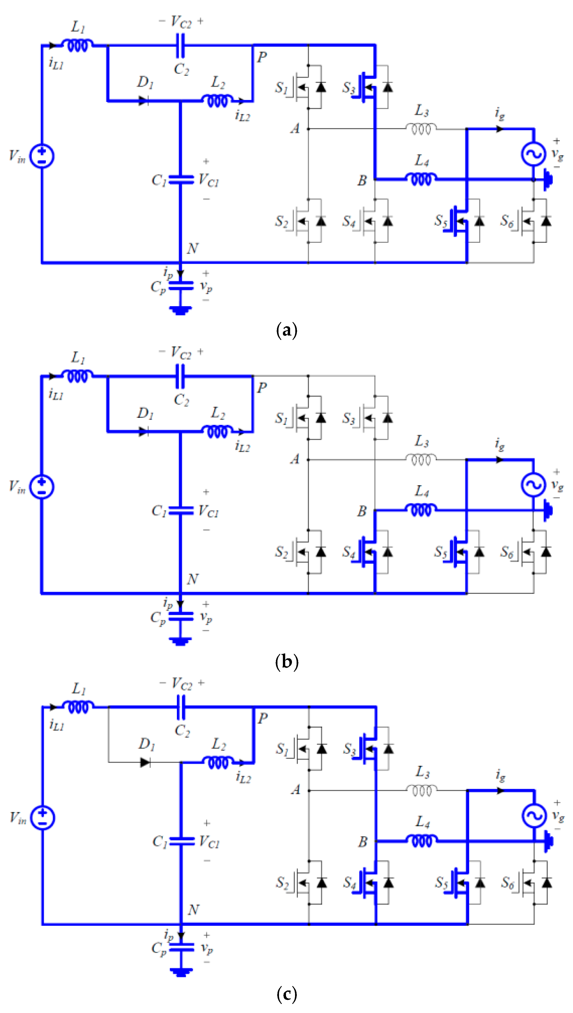
Figure 5.
Signal diagrams for S1 ~ S4 when they operate with high switching frequency.
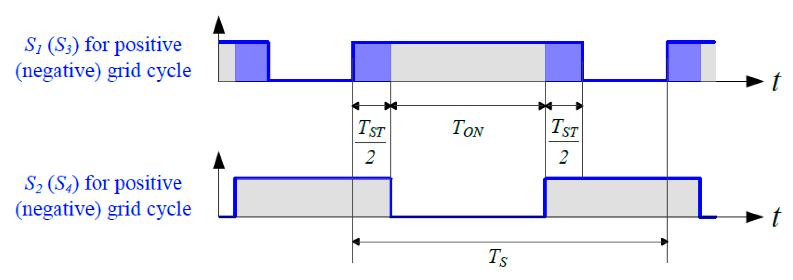
Figure 6.
Control block diagrams of the proposed inverter: (a) DC-link voltage control; (b) grid current control.
Figure 6.
Control block diagrams of the proposed inverter: (a) DC-link voltage control; (b) grid current control.

Figure 7.
Picture of the prototype inverter.

Figure 8.
Experimental waveforms: (a) vg and vp in the conventional inverter; (b) vg and ip in the conventional inverter; (c) vg and vp in the proposed inverter; (d) vg and ip in the proposed inverter.
Figure 8.
Experimental waveforms: (a) vg and vp in the conventional inverter; (b) vg and ip in the conventional inverter; (c) vg and vp in the proposed inverter; (d) vg and ip in the proposed inverter.

Figure 9.
Experimental waveforms of the proposed inverter: (a) Vin, VPN, vg, and ig; (b) Vin, VC2, and VPN; (c) Vin, VC1, VC2, and iL1.
Figure 9.
Experimental waveforms of the proposed inverter: (a) Vin, VPN, vg, and ig; (b) Vin, VC2, and VPN; (c) Vin, VC1, VC2, and iL1.

Figure 10.
Power efficiency curves: (a) when IGBTs were adopted; (b) when SiC MOSFETs were adopted.

Figure 11.
Circuit and signal diagrams of the inverter in [15]: (a) circuit diagram; (b) signal diagram for S1 ~ S4.
Figure 11.
Circuit and signal diagrams of the inverter in [15]: (a) circuit diagram; (b) signal diagram for S1 ~ S4.


© 2019 by the authors. Licensee MDPI, Basel, Switzerland. This article is an open access article distributed under the terms and conditions of the Creative Commons Attribution (CC BY) license (http://creativecommons.org/licenses/by/4.0/).
Share and Cite
MDPI and ACS Style
Choi, W.-Y.; Yang, M.-K. Transformerless Quasi-Z-Source Inverter to Reduce Leakage Current for Single-Phase Grid-Tied Applications. Electronics 2019, 8, 312. https://doi.org/10.3390/electronics8030312
AMA Style
Choi W-Y, Yang M-K. Transformerless Quasi-Z-Source Inverter to Reduce Leakage Current for Single-Phase Grid-Tied Applications. Electronics. 2019; 8(3):312. https://doi.org/10.3390/electronics8030312
Chicago/Turabian StyleChoi, Woo-Young, and Min-Kwon Yang. 2019. "Transformerless Quasi-Z-Source Inverter to Reduce Leakage Current for Single-Phase Grid-Tied Applications" Electronics 8, no. 3: 312. https://doi.org/10.3390/electronics8030312
Note that from the first issue of 2016, this journal uses article numbers instead of page numbers. See further details here.