Low Cost Test Pattern Generation in Scan-Based BIST Schemes


Abstract
1. Introduction
2. BMSIC-TPG Structure
2.1. BMSIC-TPG
2.2. LFSR Structure and Johnson Counter Structure
2.3. XOR Network
2.4. Broadcaster
2.5. The Process of BMSIC-TPG
- Clock control module generates CLK1 and CLK2. CLK1 drives the LFSR to update the seed vector, and CLK2 drives the reconfigurable Johnson counter to update the J vector and enables the scan to move in.
- Original scan chain generation module is made up of the LFSR, reconfigurable Johnson counter, and XOR network. The LFSR generates the S vector. The reconfigurable Johnson counter generates the J vector. The XOR network operates the bit-XOR between the S vector and the J vector to generate the original scan chain data.
- Broadcast module is used to extend the original scan chain.
3. BMSIC-TPG Mathematical Features
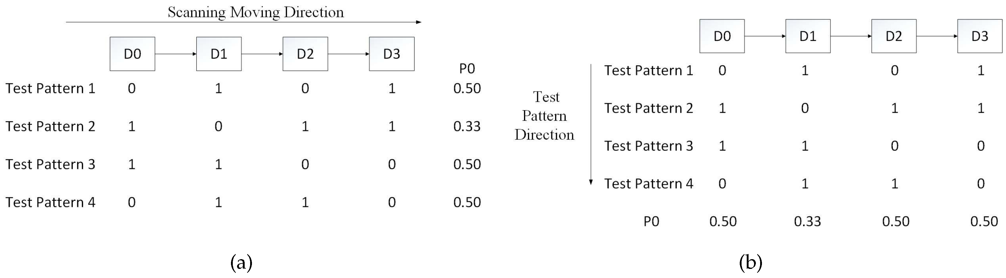
3.1. Periodicity
3.2. Transition
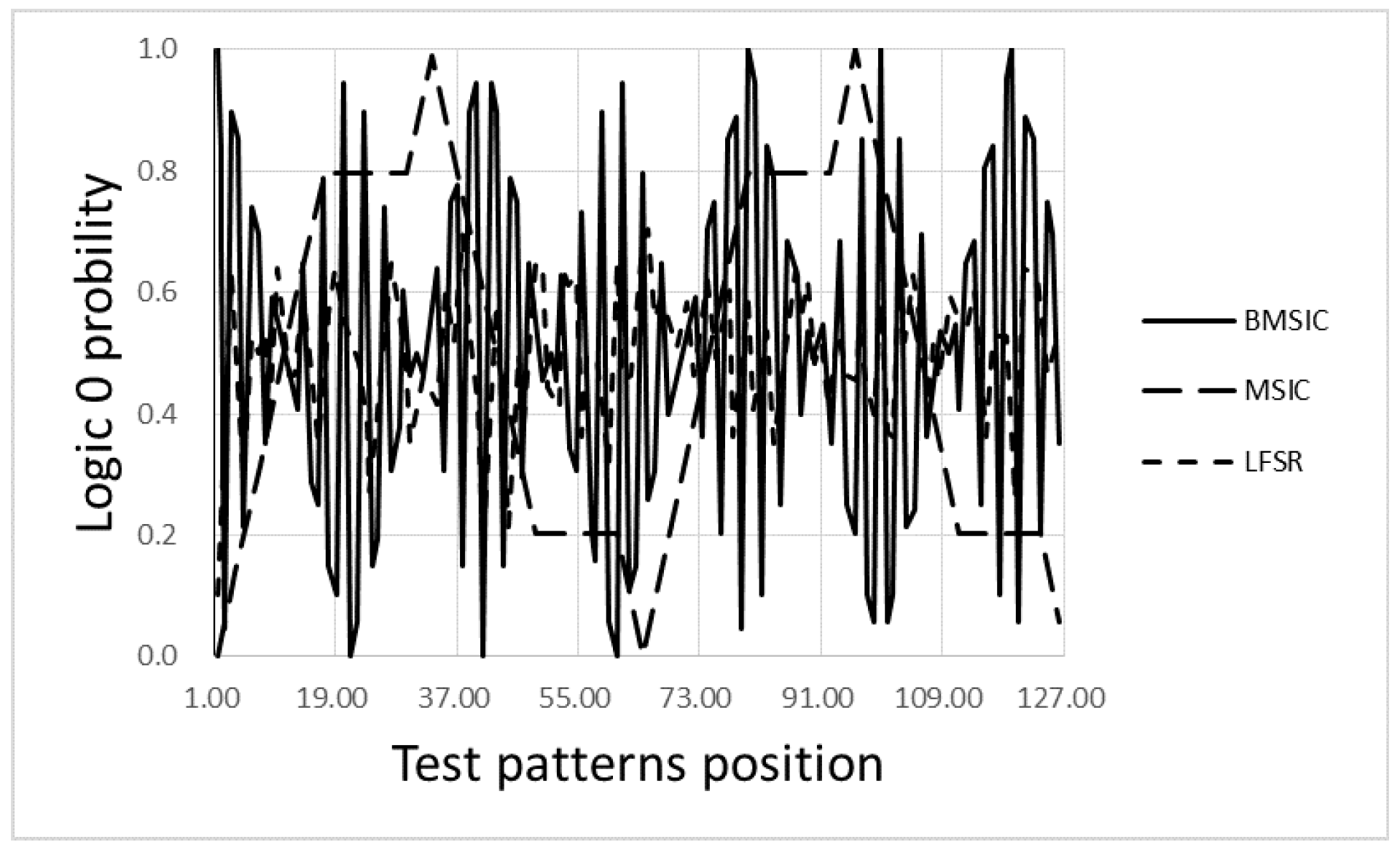
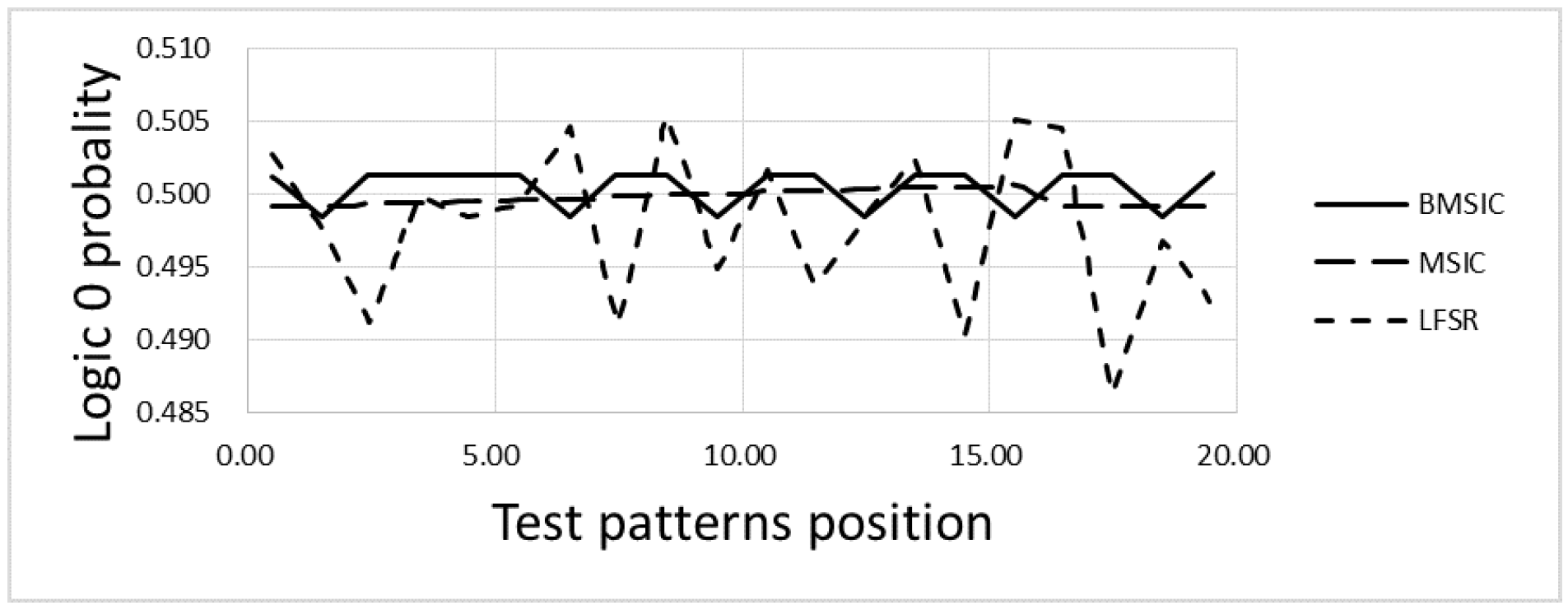
3.3. Randomness
4. BMSIC-TPG Performance Analysis
4.1. Fault Simulation
4.2. Power Consumption Simulation
4.3. Area Overhead Evaluation
5. Conclusions
Author Contributions
Funding
Conflicts of Interest
References
- Takahashi, Y.; Maeda, A. Multi Domain Test: Novel test strategy to reduce the Cost of Test. In Proceedings of the 29th VLSI Test Symposium, Dana Point, CA, USA, 1–5 May 2011; pp. 303–308. [Google Scholar]
- Dutta, A.; Kundu, S.; Chattopadhyay, S. Thermal Aware Don’t Care Filling to Reduce Peak Temperature and Thermal Variance during Testing. In Proceedings of the 2013 22nd Asian Test Symposium, Jiaosi Township, Taiwan, 8–21 November 2013; pp. 25–30. [Google Scholar]
- Puczko, M. Low power test pattern generator for BIST. In Proceedings of the 2015 Selected Problems of Electrical Engineering and Electronics (WZEE), Kielce, Poland, 7–19 September 2015; pp. 1–6. [Google Scholar]
- Bushnell, M.; Agrawal, V. Essentials of Electronic Testing for Digital, Memory and Mixed-Signal VLSI Circuits; Springer Publishing Company, Incorporated: New York City, NY, USA, 2013. [Google Scholar]
- Lei, S.C.; Shao, Z.B.; Liang, F. VLSI Testing; Publishing House of Electronic Industry: Beijing, China, 2008. [Google Scholar]
- Liang, F.; Zhang, L.; Lei, S.; Zhang, G.; Gao, K.; Liang, B. Test Patterns of Multiple SIC Vectors: Theory and Application in BIST Schemes. IEEE Trans. Very Large Scale Integr. (VLSI) Syst. 2013, 21, 614–623. [Google Scholar] [CrossRef]
- McLaurin, T. Periodic Online LBIST Considerations for a Multicore Processor. In Proceedings of the 2018 IEEE International Test Conference in Asia (ITC-Asia), Harbin, China, 15–17 August 2018; pp. 37–42. [Google Scholar]
- Shirur, Y.J.M.; Bhimashankar, B.C.; Chakravarthi, V.S. Performance analysis of low power microcode based asynchronous P-MBIST. In Proceedings of the 2015 International Conference on Advances in Computing, Communications and Informatics (ICACCI), Kochi, India, 10–13 August 2015; pp. 555–560. [Google Scholar]
- Datta, D.; Datta, B.; Dutta, H.S. Design and implementation of multibit LFSR on FPGA to generate pseudorandom sequence number. In Proceedings of the 2017 Devices for Integrated Circuit (DevIC), Kalyani, India, 23–24 March 2017; pp. 346–349. [Google Scholar]
- Seo, S.; Lee, Y.; Lee, J.; Kang, S. A scan shifting method based on clock gating of multiple groups for low power scan testing. In Proceedings of the Sixteenth International Symposium on Quality Electronic Design, Santa Clara, CA, USA, 2–4 March 2015; pp. 162–166. [Google Scholar]
- Xiang, D.; Wen, X.; Wang, L. Low-Power Scan-Based Built-In Self-Test Based on Weighted Pseudorandom Test Pattern Generation and Reseeding. IEEE Trans. Very Large Scale Integr. (VLSI) Syst. 2017, 25, 942–953. [Google Scholar] [CrossRef]
- Lee, K.J.; Chen, J.J.; Huang, C.H. Broadcasting test patterns to multiple circuits. IEEE Trans. Comput.-Aided Des. Integr. Circuits Syst. 1999, 18, 1793–1802. [Google Scholar]
- Jeníček, J.; Novák, O.; Chloupek, M. Advanced scan chain configuration method for broadcast decompressor architecture. In Proceedings of the 2011 9th East-West Design Test Symposium (EWDTS), Sevastopol, Ukraine, 9–12 September 2011; pp. 140–143. [Google Scholar]
- Gu, X.; Sheu, B.; Wang, Z.; Wang, L.; Wu, S.; Wen, X.; Jiang, Z. VirtualScan: Test Compression Technology Using Combinational Logic and One-Pass ATPG. IEEE Des. Test Comput. 2008, 25, 122–130. [Google Scholar]
- Chen, J.; Lee, K. Test Stimulus Compression Based on Broadcast Scan With One Single Input. IEEE Trans. Comput.-Aided Des. Integr. Circuits Syst. 2017, 36, 184–197. [Google Scholar] [CrossRef]
- Pomeranz, I. Computing Seeds for LFSR-Based Test Generation From Nontest Cubes. IEEE Trans. Very Large Scale Integr. (VLSI) Syst. 2016, 24, 2392–2396. [Google Scholar] [CrossRef]
- Singh, S.; Kaur, S.; Kaur, R.; Kaler, R.S. Photonic processing of all-optical Johnson counter using semiconductor optical amplifiers. IET Optoelectron. 2017, 11, 8–14. [Google Scholar] [CrossRef]
- Stoev, I.I.; Borodzhieva, A.N.; Mutkov, V.A. FPGA Implementation of Johnson Counters Applied in the Educational Process. In Proceedings of the 2018 IEEE 24th International Symposium for Design and Technology in Electronic Packaging (SIITME), Iasi, Romania, 25–28 October 2018; pp. 99–103. [Google Scholar]
- Touba, N.A. Survey of Test Vector Compression Techniques. IEEE Des. Test Comput. 2006, 23, 294–303. [Google Scholar] [CrossRef]
- Girard, P.; Landrault, C.; Pravossoudovitch, S.; Severac, D. Reducing power consumption during test application by test vector ordering. In Proceedings of the 1998 IEEE International Symposium on Circuits and Systems (Cat. No.98CH36187), ISCAS ’98, Monterey, CA, USA, 31 May–3 June 1998; Volume 2, pp. 296–299. [Google Scholar]
- Nourani, M.; Tehranipoor, M.; Ahmed, N. Low-Transition Test Pattern Generation for BIST-Based Applications. IEEE Trans. Comput. 2008, 57, 303–315. [Google Scholar] [CrossRef]


| Seed Vector Bits | Johnson Vector Bits | Transition Period | Pattern Numbers | Pattern Transitions |
|---|---|---|---|---|
| 8 | 8 | 8 | 1 | 0 |
| 7 | 56 | |||
| 8 | 17 | 17 | 1 | 0 |
| 8 | 60 | |||
| 8 | 64 | |||
| 8 | 20 | 20 | 1 | 0 |
| 8 | 60 | |||
| 11 | 64 | |||
| 10 | 10 | 10 | 1 | 0 |
| 9 | 90 | |||
| 10 | 36 | 36 | 1 | 0 |
| 10 | 76 | |||
| 25 | 80 | |||
| 10 | 44 | 44 | 1 | 0 |
| 10 | 76 | |||
| 33 | 80 |
| CUT | DFF | Chain | Depth | TL | LFSR | MSIC [6] | BMSIC | |||
|---|---|---|---|---|---|---|---|---|---|---|
| SFC | TFC | SFC | TFC | SFC | TFC | |||||
| S13207 | 638 | 32 | 20 | 10,000 | 91.44 | 80.75 | 90.51 | 74.3 | 91.42 | 74.02 |
| 36 | 18 | 10,000 | 92.01 | 80.33 | 86.63 | 71.11 | 92.6 | 73.57 | ||
| 40 | 16 | 10,000 | 95.24 | 84.05 | 89.22 | 70.82 | 93.52 | 77.71 | ||
| S15850 | 534 | 32 | 17 | 10,000 | 93.9 | 85.55 | 92.01 | 78.36 | 89.45 | 75.12 |
| 36 | 15 | 10,000 | 93.82 | 85.55 | 91.23 | 76.79 | 91.79 | 77.01 | ||
| 40 | 14 | 10,000 | 94.69 | 86.59 | 90.11 | 73.19 | 93.59 | 80.60 | ||
| S35932 | 1728 | 40 | 44 | 10,000 | 99.55 | 97.04 | 97.34 | 86.28 | 99.97 | 95.99 |
| 48 | 36 | 10,000 | 99.60 | 96.66 | 99.94 | 93.99 | 99.98 | 92.04 | ||
| 56 | 31 | 10,000 | 99.56 | 96.34 | 97.77 | 88.7 | 99.98 | 94.53 | ||
| S38417 | 1636 | 40 | 41 | 10,000 | 93.48 | 83.67 | 83.69 | 59.11 | 84.65 | 60.4 |
| 48 | 35 | 10,000 | 93.68 | 83.18 | 85.33 | 61.68 | 85.22 | 61.58 | ||
| 56 | 30 | 10,000 | 93.66 | 82.87 | 84.34 | 61.09 | 83.46 | 52.74 | ||
| S38584 | 1426 | 40 | 36 | 10,000 | 95.99 | 90.51 | 93.39 | 76.6 | 97.32 | 81.31 |
| 48 | 30 | 10,000 | 96.01 | 90.99 | 95.36 | 82.4 | 98.00 | 84.67 | ||
| 56 | 26 | 10,000 | 97.17 | 92.15 | 95.23 | 82.11 | 98.16 | 90.04 | ||
| CUT | DFF | Chain | Depth | Primepower | |||||
|---|---|---|---|---|---|---|---|---|---|
| Total () | Peak () | ||||||||
| LFSR | MSIC [6] | BMSIC | LFSR | MSIC [6] | BMSIC | ||||
| S13207 | 638 | 32 | 20 | 116.61 | 105.89 | 107.78 | 6891.83 | 5535.75 | 5582.29 |
| 36 | 18 | 116.39 | 104.75 | 107.72 | 6818.38 | 5737.82 | 5617.09 | ||
| 40 | 16 | 116.59 | 104.51 | 108.20 | 7337.72 | 5536.47 | 5617.74 | ||
| S15850 | 534 | 32 | 17 | 109.26 | 96.4 | 99.31 | 6633.73 | 5137.78 | 5429.68 |
| 36 | 15 | 108.59 | 95.13 | 99.41 | 6518.92 | 5026.07 | 5396.98 | ||
| 40 | 14 | 109.09 | 94.8 | 99.13 | 6656.53 | 5442.83 | 5345.9 | ||
| S35932 | 1728 | 40 | 44 | 320.86 | 276.83 | 272.26 | 20,835.3 | 17,317.1 | 19,303.6 |
| 48 | 36 | 322.54 | 275.91 | 277.25 | 21,014.8 | 14,695.9 | 19,864.5 | ||
| 56 | 31 | 322.22 | 274.54 | 282.07 | 21,380.5 | 25,411.3 | 20,922.4 | ||
| S38417 | 1636 | 40 | 41 | 347.57 | 280.81 | 286.98 | 20,349.8 | 17,630.4 | 17,503.9 |
| 48 | 35 | 347.32 | 282.52 | 286.92 | 20,578.5 | 17,081.9 | 16,952.8 | ||
| 56 | 30 | 346.68 | 280.41 | 289.17 | 19,979 | 17,425.5 | 17,150.1 | ||
| S38584 | 1426 | 40 | 36 | 335.26 | 286.89 | 292.9 | 21,125.5 | 15,583.2 | 18,163.6 |
| 48 | 30 | 335.46 | 287.13 | 293.95 | 20,058.9 | 15,768.9 | 17,835.2 | ||
| 56 | 26 | 335.43 | 285.67 | 291.39 | 20,011.9 | 16,110.7 | 15,692.3 | ||
| CUT | Chain | Depth | LFSR | MSIC [6] | BMSIC | Reduction (%) | ||||||
|---|---|---|---|---|---|---|---|---|---|---|---|---|
| S | L | Area | S | L | Area | S | L | Area | ||||
| S13207 | 32 | 20 | 32 | 0 | 94 | 32 | 32 | 218 | 8 | 20 | 131 | 39.9 |
| 36 | 18 | 36 | 0 | 103 | 36 | 36 | 243 | 9 | 18 | 131 | 46.09 | |
| 40 | 16 | 40 | 0 | 116 | 40 | 40 | 271 | 10 | 16 | 133 | 50.92 | |
| S15850 | 32 | 17 | 32 | 0 | 94 | 32 | 32 | 218 | 8 | 17 | 122 | 44.04 |
| 36 | 15 | 36 | 0 | 103 | 36 | 36 | 243 | 9 | 15 | 122 | 49.79 | |
| 40 | 14 | 40 | 0 | 116 | 40 | 40 | 271 | 10 | 14 | 127 | 53.14 | |
| S35932 | 40 | 44 | 40 | 0 | 116 | 40 | 44 | 283 | 10 | 44 | 212 | 25.09 |
| 48 | 36 | 48 | 0 | 139 | 48 | 48 | 325 | 12 | 36 | 207 | 36.31 | |
| 56 | 31 | 56 | 0 | 161 | 56 | 56 | 378 | 14 | 31 | 209 | 44.71 | |
| S38417 | 40 | 41 | 40 | 0 | 116 | 40 | 41 | 274 | 10 | 41 | 204 | 25.55 |
| 48 | 35 | 48 | 0 | 139 | 48 | 48 | 325 | 12 | 35 | 205 | 36.92 | |
| 56 | 30 | 56 | 0 | 161 | 56 | 56 | 378 | 14 | 30 | 206 | 45.5 | |
| S38584 | 40 | 36 | 40 | 0 | 116 | 40 | 40 | 271 | 10 | 36 | 190 | 29.89 |
| 48 | 30 | 48 | 0 | 139 | 48 | 48 | 325 | 12 | 30 | 190 | 41.54 | |
| 56 | 26 | 56 | 0 | 161 | 56 | 56 | 378 | 14 | 26 | 195 | 48.41 | |
© 2019 by the authors. Licensee MDPI, Basel, Switzerland. This article is an open access article distributed under the terms and conditions of the Creative Commons Attribution (CC BY) license (http://creativecommons.org/licenses/by/4.0/).
Share and Cite
Zhang, G.; Yuan, Y.; Liang, F.; Wei, S.; Yang, C.-F. Low Cost Test Pattern Generation in Scan-Based BIST Schemes. Electronics 2019, 8, 314. https://doi.org/10.3390/electronics8030314
Zhang G, Yuan Y, Liang F, Wei S, Yang C-F. Low Cost Test Pattern Generation in Scan-Based BIST Schemes. Electronics. 2019; 8(3):314. https://doi.org/10.3390/electronics8030314
Chicago/Turabian StyleZhang, Guohe, Ye Yuan, Feng Liang, Sufen Wei, and Cheng-Fu Yang. 2019. "Low Cost Test Pattern Generation in Scan-Based BIST Schemes" Electronics 8, no. 3: 314. https://doi.org/10.3390/electronics8030314
APA StyleZhang, G., Yuan, Y., Liang, F., Wei, S., & Yang, C.-F. (2019). Low Cost Test Pattern Generation in Scan-Based BIST Schemes. Electronics, 8(3), 314. https://doi.org/10.3390/electronics8030314