A Compact Broadband Monolithic Sub-Harmonic Mixer Using Multi-Line Coupler

1
Institute of VLSI Design, College of Electrical Engineering, Zhejiang University, Hangzhou 310027, China
2
Key Laboratory of RF Circuits and Systems, Ministry of Education, Hangzhou Dianzi University, Hangzhou 310018, China
3
The 41st Institute of China Electronics Technology Group Corporation, Qingdao 266555, China
*
Author to whom correspondence should be addressed.
Electronics 2020, 9(4), 694; https://doi.org/10.3390/electronics9040694
Submission received: 9 April 2020
/
Revised: 17 April 2020
/
Accepted: 21 April 2020
/
Published: 24 April 2020
(This article belongs to the Special Issue Millimeter-Wave Integrated Circuits and Systems for 5G Applications)
Abstract
:A compact broadband monolithic sub-harmonic mixer is presented in a 70 nm GaAs Technology for millimeter wave wireless communication application. The proposed mixer adopts a novel multi-line coupler structure; where the two-sided coupling energy of radio frequency (RF) and local oscillation (LO) signals are both collected and efficiently feed to anti-parallel diode pair (APDP) topology; resulting in broadband performance and compact chip size. As a comparison in the same circuit configuration; the five-line coupler can expand the bandwidth of the existing three-line coupler by 85% and reduce the area by 39.5% when the central frequency is 127 GHz. The measured conversion gain is −16.2 dB to −19.7 dB in a wide operation frequency band of 110–170 GHz. The whole chip size is 0.47 × 0.66 mm2 including test pads. The proposed mixer exhibits good figure-of-merits for D-band down-converter applications
1. Introduction
With the rapid development of real-time or high-definition video interaction and cloud computing services, the existing 3G and 4G wireless communication systems are difficult to meet the growing needs of more and more services. In order to increase the communication capacity, expanding the bandwidth becomes the first choice. In addition to using carrier aggregation technology to expand the bandwidth in sub-6 GHz band, it has become an inevitable trend to extend to a higher frequency band. Because of its wide operating bandwidth, millimeter wave band can achieve high-speed data transfer capability suitable for the fifth generation (5G) and the next generation of wireless communication [1]. Especially over 100 GHz band, which has not been formally arranged in the spectrum division of mobile wireless communication, may become the main choice of the next generation of wireless communication.
The mixer is one of the key circuits in millimeter wave front-end system, which is responsible for converting millimeter wave signal to intermediate frequency (IF) signal. With good conversion gain, compact size, and superior spur rejection, the fundamental mixer is widely used in modern CMOS radio frequency integration circuits, and further extended to 5G transceiver front-end in millimeter wave band [2,3]. In comparison to the fundamental mixer, the sub-harmonic mixer can decrease the LO frequency by half or several times, thus reduce the requirements of high-performance signal source, especially when the circuit operating frequency is greater than 100 GHz. Moreover, the sub-harmonic mixer avoids the LO self-mixing problem which are caused by LO leakage to the RF port, and then generate a DC offset at the IF port. Therefore, the sub-harmonic mixers are very suitable in the millimeter wave broadband communication system [4,5].
The sub-harmonic mixer is usually realized by using the nonlinear characteristics of active transistor such as field effect transistor (FET) and bipolar transistor or varactor diode device. The mixer based on active device can achieve better frequency conversion gain, but it will be accompanied by larger noise and additional DC power consumption [6,7]. The sub-harmonic mixer with diode has simple circuit structure and zero power consumption, so it is widely used in millimeter wave band [8,9,10,11,12,13,14,15,16,17]. The most typical circuit such as 78–114 GHz sub-harmonic mixer utilizes quarter-wavelength open-stub and short-stub at each end of the diodes pair to achieve good isolation between LO and RF ports, but it also brings a large chip area of 3 mm2 [9]. In order to reduce the area, some designs adopt the way of bending transmission lines, but also lead to the limited bandwidth of 30 GHz and 20 GHz respectively [14,15]. The FET without drain voltage can also be used to design and implement passive sub-harmonic mixers without additional DC power consumption [18,19,20,21,22]. Among them, the best circuit achieves a measured conversion loss between 12.5 dB and 16 dB in the radio frequency bandwidth from 120 GHz to 150 GHz, but it also takes up a large area of 1.8 mm2 due to the Lange coupler and λ/4 transmission line [20].
Previous studies have shown that for sub-harmonic mixers using a parallel grounded APDP configuration, RF and LO are respectively connected to a common end of the diodes through two-line coupler matching networks [12], and three transmission line coupler is used firstly to simultaneously excite an RF and LO signal into the APDP for 18–40 GHz band application [23], and then extended to millimeter wave sub-harmonic mixer design above 100 GHz [17]. However, because the operating frequency and bandwidth of the transmission line are sensitive to its physical length, the coupler will directly limit the operation bandwidth of millimeter wave band and the conversion gain of the RF signal. In this study, a novel multi-line coupler configuration is proposed to overcome these problems and to achieve a broadband performance.
In this paper, a compact and broadband sub-harmonic mixer is proposed by using APDP with parallel to ground structure and a novel multi-line coupler. The multi-line coupler structure is used to efficiently feed RF and LO signals to the APDP topology to lead to broadband performance and compact chip size of the mixer. The measured results show that the present mixer can operate in D-band range with a good conversion gain, broad bandwidth and compact size including GSG pads.
2. Circuit Design
2.1. Mixer Topology
Figure 1 illustrates the schematic of the present sub-harmonic mixer. The whole circuit is composed of a parallel grounded APDP mixing core, a multi-line coupler, an LO match circuit and an IF low pass filter (LPF). The mixing mechanism of the sub-harmonic mixer is implemented between the RF signal and the second harmonic of the LO signal. Compared with the serial configuration of APDP, the parallel ground mixing core directly offers DC ground paths to minimize the chip area, removing the short-circuited stub.
The diode is implemented of HEMT transistor, in which the gate is as the anode and the drain and source connected together is as the cathode. The diode parameters of the APDP are selected as gate length of 3 μm and gate width of 2 × 13 μm respectively for good conversion loss and wide operation bandwidth, and even-harmonic suppression performance. Meanwhile, a self-built diode model is used to aid circuit design, consisting of the intrinsic diode junction non-linearity model and parasitic passive equivalent-circuit network, which can match the measured data to 220 GHz [15].
The LO matching and IF LPF circuits are realized by using microstrip line and capacitor. In the Figure 1, all the length of microstrip line is expressed by the electrical length when the central frequency is 127 GHz.
2.2. Coupler Design
In the three-line coupler as shown in Figure 2a, the LO and RF signals are respectively edge-coupled from both sides of the middle line, and since there is only one side coupling between RF and LO to the mixing core, there exists coupling energy leakage on the other side of RF and LO. Ideally, half of the coupling energy may be wasted in space. In this paper, multi-line coupler is adopted to collect the desired signals on the other side of RF and LO, as shown in Figure 2b–d. Figure 2b represents the multi-line coupler with two-sided collection of LO signal (named 4Lines_LO), and Figure 2c represents the multi-line coupler with two-sided collection of RF signal (named 4Lines_RF), and Figure 2d represents the multi-line coupler with simultaneous two-sided collection of LO and RF signals (named 5Lines). Thus, by collecting more coupling energy from LO or RF or LO and RF together, the multi-line coupler can inject more signals into the diode pair. Conversely, the length of the coupler can be reduced or folded in the direction of signal propagation. Meanwhile, since the frequency sensitivity of smaller physical length is lower, the multi-line coupler can reduce the area and expand the operating bandwidth at the same time.
In order to have an intuitive understanding, the transmission characteristics of RF to diode pair and lo to diode pair of multi coupler are respectively simulated in electromagnetic field, as shown in Figure 3. The detailed parameters of couplers are shown in Table 1. The load port of the coupler is connected to resistance used in the circuit (130 Ω), the diode pair port of the coupler is matched to its conjugate impedance, and both RF and LO ports are terminated to 50 Ω. It can be seen that the RF to diode pair transmission characteristics of the 5Lines coupler are basically the same as that of the 4Lines_RF coupler, and both are better than that of the 3Lines coupler. Moreover, the LO to diode pair transmission characteristics of the 5Lines coupler are basically the same as that of the 4Lines_LO coupler, and both are better than that of the 3Lines coupler, especially in the 40–90 GHz fundamental frequency band improved by 3.7 to 5.3 dB. The simulation results verify the feasibility of the previous theoretical analysis, that is, more coupling energy can enter the diode pair through the two-sided coupling of RF and LO signals.
In order to show the effect of different multi-line couplers on mixing performance, sub-harmonic mixers based on different multi-line couplers were designed and simulated. It should be noted that the mixer realized by the three-line coupler of the same length will operate at higher frequencies band, so a longer optimized three-line coupler design of 92-degree electrical length at 127 GHz (215 μm length) is also compared. The conversion gains of full wave electromagnetic field simulation results are shown in Figure 4. It can be found, the 5Lines case has maximum 3 dB bandwidth is 98 GHz of 78 GHz to 176 GHz, and the 3Lines case with 215 μm length has 3 dB bandwidth is 53 GHz of 101 GHz to 154 GHz. The comparison shows that, the five-line coupler can reduce the area of the three-line coupler by 39.5% and expands the bandwidth by 85% when the central frequency is 127 GHz. Meanwhile, the conversion gain of 4Lines_LO case is better than that of 4Lines_RF case, which shows that the coupling energy of collecting LO is more effective than that of collecting RF, and that LO power has a greater impact on mixing efficiency.
Moreover, for the five-line coupler case, the effects of different spaces between the outer microstrip lines on both sides and LO and RF are also compared, that is, the parameter values of S1 and S2 in Figure 2d are reduced from 30 μm to 3 μm, and the corresponding simulated conversion gains are shown in Figure 4. It can be found that with the decrease of spacing, LO and RF can couple more energy to the diode pair, and the conversion gain performance of mixer is better.
2.3. IF Filter Design
At the IF output port, the LPF consists of a series microstrip line (L4), a parallel open stub branch (L5) along with a shunt grounded metal-insulator-metal (MIM) capacitor (C1) for the RF/LO-to-IF isolations and extracts the IF signal. The electromagnetic field simulation results show that the transmission loss of the LPF is less than 1 dB when the frequency is within 20 GHz, and more than 20 dB when the frequency is above 80 GHz, as shown in Figure 5. It can be found that the circuit can achieve effective suppression of the LO and RF leakage and keep a wide pass band performance for IF signal.
2.4. Layout Design
The present sub-harmonic mixer was fabricated in a 70 nm mHEMT process of GaAs semi-insulating substrate with thickness 100 μm and the relative permittivity 12.9. The field effect transistor achieves ft/fmax value above 300 GHz, and the process offers two gold metal layers, top metal and bottom metal, with the thickness is 1.25 μm and 0.65 μm respectively. Meandering or folding microstrip lines are used to reduce the chip area. All passive components including multi-line coupler, microstrip lines, MIM capacitor, resistor, signal pads and back-vias are designed and optimized in Advanced design system (ADS) software of Keysight for schematic and EM co-simulation. The microscope photograph of the fabricated sub-harmonic mixer is given in Figure 6 and the chip size is as compact as 0.47 × 0.66 mm2 including GSG test pads.
3. Measurements and Discussion
3.1. Test Configuration
The circuit is tested thru on-chip probing and the measurement setup is shown in Figure 7. The RF input signal of 110 GHz to 170 GHz was generated by analog signal generator (Agilent E8257D) cascaded with D-band ×12 frequency multiplier module (VDI SGX WR6.5), and then the output power was reduced to –20 dBm through a D-band attenuator (Elmika VA-02E-G) and a D-band isolator (Millitech FBI-06). The LO input signal was generated in two ways at different frequencies. In 55 GHz to 75 GHz frequency band, the LO signal was produced by vector signal generator (Agilent E8257C) cascaded with V-band ×4 frequency multiplier module (VDI SGX WR15) and a V-band isolator (Millitech FBI-15), and for 75 GHz to 85 GHz frequency band, it was produced to the probe by the same vector signal generator (Agilent E8257C) cascaded with W-band ×6 frequency multiplier module (VDI SGX WR10). The IF signal was directly measured with signal analyzer (Keysight EXA N9010A), and the isolation signals were measured with the signal analyzer and the power meter (VDI PM4). The loss of cable, waveguide connector and probe were de-embedding with the signal source and the power meter, and the measured reference plane was calibrated to the probe tip.
3.2. Mixer Performance
Figure 8 shows the measured and simulated conversion gain as a function of the LO power level at an RF input power of –20 dBm and a fixed IF of 1GHz. A significant mixing effect of an LO drive level of 10 dBm was observed, and the variations of the conversion gain are less than 5 dB with the power level of LO signal increasing from 11 dBm to 16 dBm. The maximum conversion gain is –16.2 dB at an LO power level of 14 dBm and RF frequency of 150 GHz, and the conversion gain remains basically stable despite increased LO power. The following measurements are done based on the optimal LO power of 14 dBm.
Figure 9 illustrates the measured and simulated conversion gain of the sub-harmonic mixer as a function of RF for the down-converter mode. The experiment was implemented while simultaneously sweeping LO and RF frequencies with a fixed IF of 1 GHz. The obtained conversion gain ranged from –16.2 to –19.6 dB within the RF bandwidth range of 110 to 170 GHz and the maximum value occurs at 150 GHz. The measured results well agree with the simulated data, verifying the availability of device model and circuit design for broadband millimeter-wave applications.
It should be noted that because the output power of the W-band frequency multiplier module is not enough to drive the mixer to the optimal performance, the conversion gain test data in the 150–170 GHz band may be relatively low. According to the data provided by the manufacturer, the output power of W-band frequency multiplier module is about 14.5 to 15 dBm. Considering the loss of waveguide connector of about 0.5dB and probe loss of about 1.5 dB, the LO power reaching the probe tip is about 12.5 to 13 dBm. From the relationship between the LO power and the conversion gain as shown in Figure 7, this LO power is about 1 to 1.5 dB lower than the optimal drive power, so that the conversion gain estimated by the test is about 1dB lower than the real value.
Figure 10 shows measured the isolation related to RF frequency. From 110 GHz to 170 GHz, the measured LO-to-RF and LO-to-IF isolations are more than 18.7 dB and 23.6 dB, respectively. The trend of the measured curve is in well agreement with the simulation, while the former is 1 to 3.2 dB worse than the latter in the D-band. The difference between testing and simulation results may come from three aspects. One is the influence of the device model, especially the accuracy of the diode large signal model will have a direct impact on the nonlinear performance of the circuit. The second aspect is the process parameters, especially the dielectric properties of the dielectric layer and substrate in the millimeter wave band, such as loss tangent parameters, which will affect the accuracy of circuit simulation. The third difference may come from the difference in the test and calibration process, especially in connection or interface configuration, which will lead to test errors. Meanwhile, the 2LO-to-RF and 2LO-to-IF isolations are relatively low and submerged in noise floor of the signal analyzer, which indicates the second harmonic component of the LO signal is greatly suppressed.
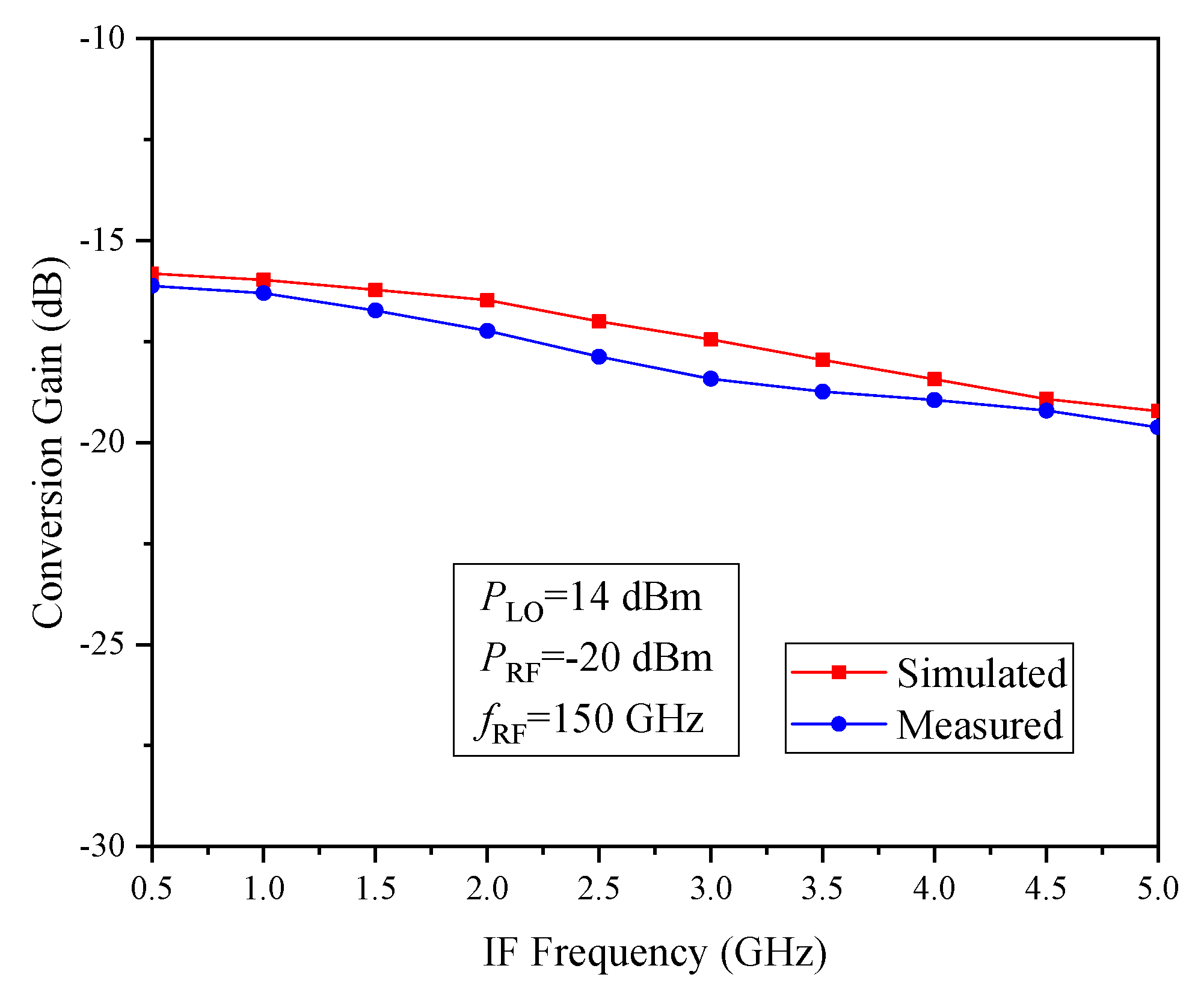
Figure 11 shows the measured and simulated conversion gain versus the IF frequency from 0.5 GHz to 5 GHz. The experiments were implemented by sweeping LO frequencies and test the corresponding IF output with a RF frequency of 150 GHz for the down-conversion mode. Providing a LO power of 14 dBm, the down-conversion mixer demonstrates a 3-dB demodulation bandwidth of 4 GHz.
Lastly, two figure-of-merits (FOMs) defined in reference [24,25] is used to evaluate different designs. Both the FOMs are suitable for the mixers, and FOM1 is a pure technical performance index, which emphasizes the contribution of gain and bandwidth. The larger the gain, the wider the bandwidth, then the better of the FOM1. On this basis, FOM2 increases the impact of area to get a more cost-effective indicator. Because the format of the test data provided by each design is not uniform, the measured bandwidth is used instead of 3 dB bandwidth to calculate the FOMs formula as follows.
where CG denotes the conversion gain in dB, BW is the measured bandwidth in GHz and the area represents the chip size in mm2.
Table 2 summarizes the performances comparison of the present circuit with the previous published passive sub-harmonic mixers above 100 GHz based on different process. It’s worth noting that as an intuitive comparison, the circuit design using the 3Lines (215 um) coupler in Figure 4 has achieved a bandwidth of 110–145 GHz [17]. Compared with previous reports, the proposed sub-harmonic mixer exhibits a good performance in terms of the operating bandwidth covering the whole D-band, the minimum area size, and FOMs. Due to the lack of W-band attenuator, the characteristics of the sub-harmonic mixer in W-band was not tested, and the simulation results are given in Table 2, which shows that the circuit has the potential capacity in W-band and D-band applications.
4. Conclusions
A broadband monolithic MMIC sub-harmonic mixer with a novel multi-line coupler was designed for millimeter-wave down-converter applications. This mixer was fabricated with the 70 nm GaAs MMIC technology. The present sub-harmonic mixer can operate at a wide frequency range of D-band with good conversion gain and compact size characteristic. The proposed mixer exhibits superior figure-of-merits, making it relatively suitable for D-band wireless communication systems.
Author Contributions
J.W. and S.Z. completed the methodology and design; J.W. wrote the paper. L.S. reviewed the paper. All authors have read and agreed to the published version of the manuscript.
Funding
This research was funded by the National Natural Science Foundation of China under grant 61674047 and 61827806.
Conflicts of Interest
The authors declare no conflict of interest.
References
- Noël, D.M.; Patrick, R. A 120 GHz Fully Integrated 10 Gb/s Short-Range Star-QAM Wireless Transmitter with On-Chip Bondwire Antenna in 45 nm Low Power CMOS. IEEE J. Solid-State Circuits 2014, 49, 1606–1616. [Google Scholar]
- Chen, J.H.; Kuo, C.C.; Hsin, Y.M.; Wang, H. A 15–50 GHz broadband resistive FET ring mixer using 0.18-μm CMOS technology. In Proceedings of the IEEE MTT-S International Microwave Symposium, Anaheim, CA, USA, 23–28 May 2010. [Google Scholar]
- Won, Y.-S.; Kim, C.-H.; Lee, S.-G. A 24 GHz Highly Linear Up-Conversion Mixer in CMOS 0.13 μm Technology. IEEE Microw. Wirel. Components Lett. 2015, 25, 400–402. [Google Scholar] [CrossRef]
- Dahlback, R.; Bryllert, T.; Granstrom, G.; Ferndahl, M.; Drakinskiy, V.; Stake, J. Compact 340 GHz homodyne transceiver modules for FMWC imaging radar arrays. In Proceedings of the 2016 IEEE MTT-S International Microwave Symposium (IMS), San Francisco, CA, USA, 22–27 May 2016. [Google Scholar] [CrossRef]
- Ji, G.; Zhang, D.; Meng, J.; Liu, S.; Yao, C. A Novel 183 GHz Solid-State Sub-Harmonic Mixer. Electronics 2020, 9, 186. [Google Scholar] [CrossRef] [Green Version]
- Seyedhosseinzadeh, N.; Nabavi, A.; Carpenter, S.; He, Z.S.; Bao, M.; Zirath, H. A 100–140 GHz SiGe-BiCMOS sub-harmonic down-converter mixer. In Proceedings of the 2017 12th European Microwave Integrated Circuits Conference (EuMIC), Nuremberg, Germany, 8–10 October 2017. [Google Scholar]
- Li, Y.; Zhang, Y.; Li, X.; Chen, Y.; Xiao, F.; Cheng, W.; Sun, Y.; Lu, H.; Xu, R. A High Conversion Gain 210-GHz InP DHBT Sub-Harmonic Mixer Using Gain-Enhanced Structure. IEEE Access 2019, 7, 101453–101458. [Google Scholar] [CrossRef]
- Siegel, P.; Weinreb, S.; Duncan, S.; Berk, W.; Eskandarian, A.; Tu, D.-W. Design and measurements of a 210 GHz subharmonically pumped GaAs MMIC mixer. In Proceedings of the 1992 IEEE Microwave Symposium Digest MTT-S, Albuquerque, NM, USA, 1–5 June 1992. [Google Scholar] [CrossRef]
- Hwang, Y.-J.; Lien, C.-H.; Wang, H.; Sinclair, M.W.; Gough, R.G.; Kanoniuk, H.; Chu, T.-H. A 78–114 GHz monolithic sub-harmonically pumped GaAs-based HEMT diode mixer. IEEE Microwave Wireless Compon. Lett. 2002, 12, 209–211. [Google Scholar] [CrossRef]
- Kok, Y.-L.; Wang, H.; Barsky, M.; Lai, R.; Sholley, M.; Allen, B. A 180-GHz monolithic sub-harmonic InP-based HEMT diode mixer. IEEE Microw. Guid. Wave Lett. 1999, 9, 529–531. [Google Scholar] [CrossRef]
- Archer, J.W.; Tello, J. A 180-196 GHz image-reject Schottky-diode MMIC mixer. Microw. Opt. Technol. Lett. 2007, 49, 2319–2322. [Google Scholar] [CrossRef]
- Kok, Y.-L.; Huang, P.-P.; Wang, H.; Allen, B.; Lai, R.; Sholley, M.; Gaier, T.; Mehdi, I. 120 and 60 GHz monolithic InP-based HEMT diode sub-harmonic mixer. In Proceedings of the 1998 IEEE MTT-S International Microwave Symposium Digest (Cat. No.98CH36192), Baltimore, MD, USA, 7–12 June 1998. [Google Scholar] [CrossRef]
- Lei, M.-F.; Wang, H. A 100-120 GHz quadruple-LO pumped harmonic diode mixer using standard GaAs based 0.15-/spl mu/m PHEMT process. In Proceedings of the 2005 Asia-Pacific Microwave, Suzhou, China, 4–7 December 2005. [Google Scholar] [CrossRef]
- Wen, J.C.; Zhang, S.Z.; Zhou, T.; Sun, L.L. A 110-140GHz Monolithic Sub-Harmonic Mixer with an APDP Topology. Nanosci. Nanotechnol. Lett. 2017, 9, 679–684. [Google Scholar]
- Ullrich, R.P.; Chinmaya, M.; Robert, M.R.; Shawn, P.; Scott, K.R. Schottky Barrier Diode Circuits in Silicon for Future Millimeter-Wave and Terahertz Applications. IEEE Trans. Microwave Theory Tech. 2008, 56, 364–371. [Google Scholar]
- Sun, Y.; Scheytt, C.J. A 122 GHz Sub-Harmonic Mixer with a Modified APDP Topology for IC Integration. IEEE Microw. Wirel. Components Lett. 2011, 21, 679–681. [Google Scholar] [CrossRef]
- Zhang, S.; Sun, L.; Wang, X.; Wen, J.; Liu, J. A compact D-band monolithic APDP-based sub-harmonic mixer. Solid-State Electron. 2017, 137, 62–69. [Google Scholar] [CrossRef]
- Archer, J.W.; Shen, M.G. 176-200-GHz receiver module using indium phosphide and gallium arsenide MMICs. Microw. Opt. Technol. Lett. 2004, 43, 458–462. [Google Scholar] [CrossRef]
- Koch, S.; Guthoerl, M.; Kallfass, I.; Leuther, A.; Saito, S. A 120–145 GHz Heterodyne Receiver Chipset Utilizing the 140 GHz Atmospheric Window for Passive Millimeter-Wave Imaging Applications. IEEE J. Solid-State Circuits 2010, 45, 1961–1967. [Google Scholar] [CrossRef]
- Campos-Roca, Y.; Tessmann, A.; Massler, H.; Leuther, A. A D-Band Sub-harmonically-Pumped Resistive Mixer Based on a 100 nm mHEMT Technology. ETRI J. 2011, 33, 818–821. [Google Scholar] [CrossRef]
- López-Díaz, D.; Kallfass, I.; Tessmann, A.; Leuther, A.; Massler, H.; Schlechtweg, M.; Ambacher, O. Subharmonically Pumped 210 GHz I/Q Mixers. In Proceedings of the 2010 IEEE Compound Semiconductor Integrated Circuit Symposium (CSICS), Monterey, CA, USA, 3–6 October 2010. [Google Scholar] [CrossRef]
- Karandikar, Y.; Zirath, H.; Yan, Y.; Vassilev, V. Compact Integration of Sub-Harmonic Resistive Mixer with Differential Double Slot Antenna in G-Band Using 50nm InP-HEMT MMIC Process. In Proceedings of the 2012 IEEE Compound Semiconductor Integrated Circuit Symposium (CSICS), La Jolla, CA, USA, 14–17 October 2012. [Google Scholar] [CrossRef]
- Yan, P.; Chen, J.; Hong, W. A miniaturized monolithic 18–40 GHz sub-harmonic mixer. J. INFRARED MILLIM TE 2010, 31, 690–696. [Google Scholar] [CrossRef]
- Liao, H.-Y.; Tseng, C.-M.; Chiou, H.-K. Lossy LC ladder matching network for ultra-wideband CMOS Gilbert cell mixer design. Microw. Opt. Technol. Lett. 2007, 50, 220–222. [Google Scholar] [CrossRef]
- Fei, W.; Yu, H.; Lim, W.M.; Ren, J. A 53-to-73GHz power amplifier with 74.5mW/mm2 output power density by 2D differential power combining in 65nm CMOS. In Proceedings of the 2013 IEEE Radio Frequency Integrated Circuits Symposium (RFIC), Seattle, WA, USA, 2–4 June 2013. [Google Scholar] [CrossRef]
Figure 1.
The schematic of the present anti-parallel diode pair (APDP)-based sub-harmonic mixer.

Figure 2.
(a) three-line coupler (3Lines), (b) multi-line coupler with two-sided coupled local oscillation (LO) signal (4Lines_LO), (c) multi-line coupler with two-sided coupled radio frequency (RF) signal (4Lines_RF), and (d) multi-line coupler with simultaneous two-sided coupled LO and RF signals (5Lines).
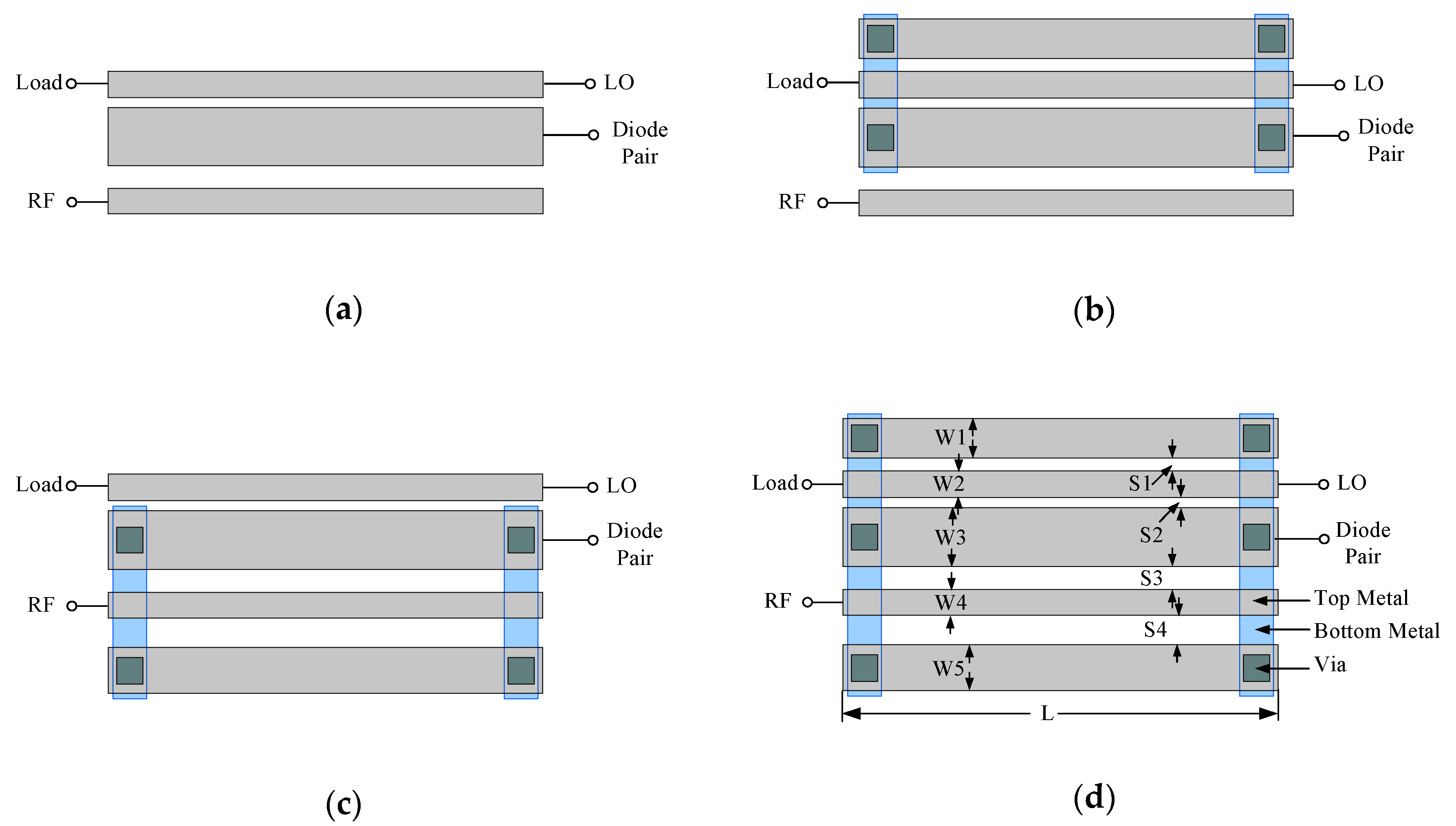
Figure 3.
The simulated transmission characteristics of (a) RF to Diode Pair and (b) LO to Diode Pair.
Figure 3.
The simulated transmission characteristics of (a) RF to Diode Pair and (b) LO to Diode Pair.
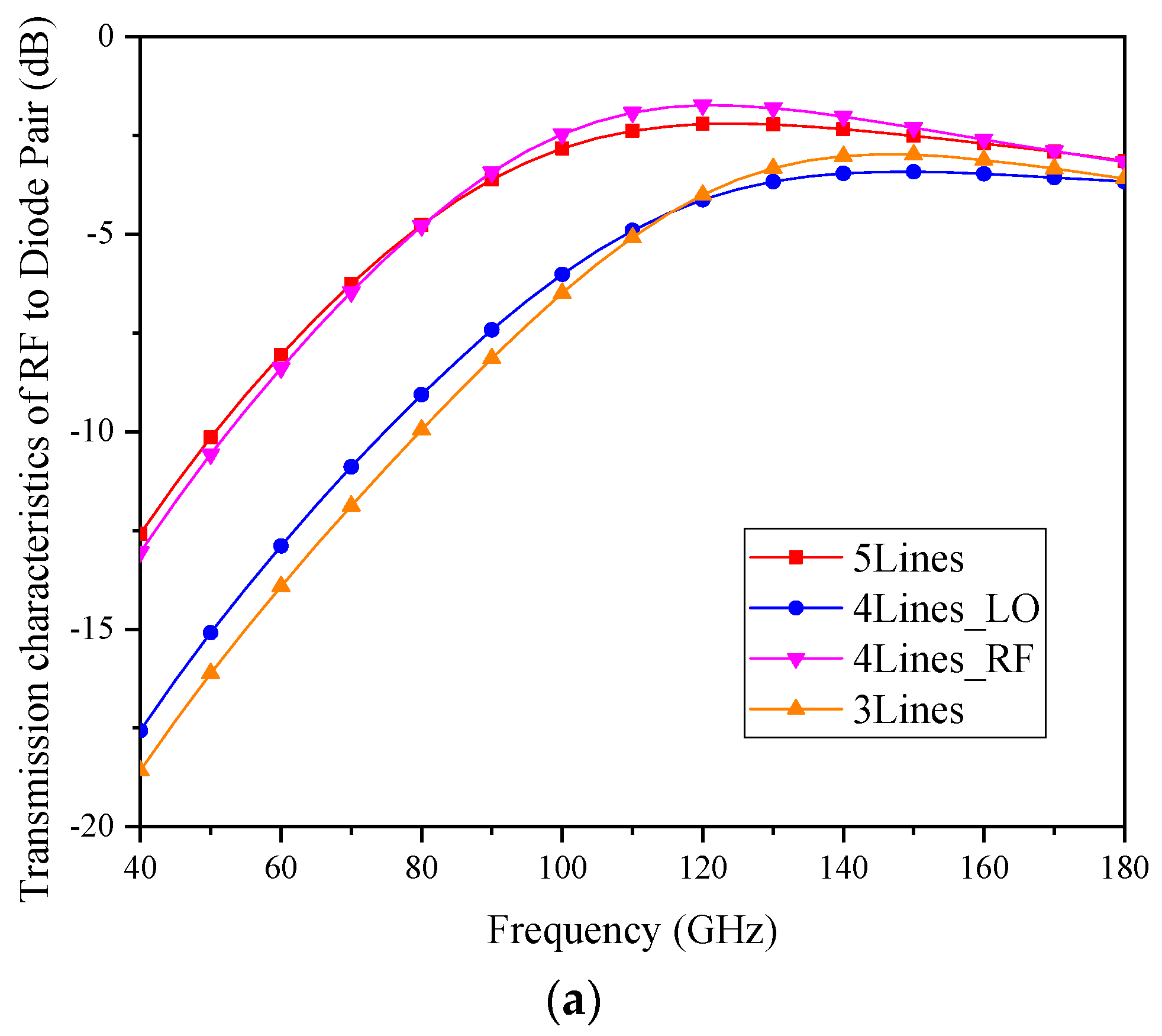
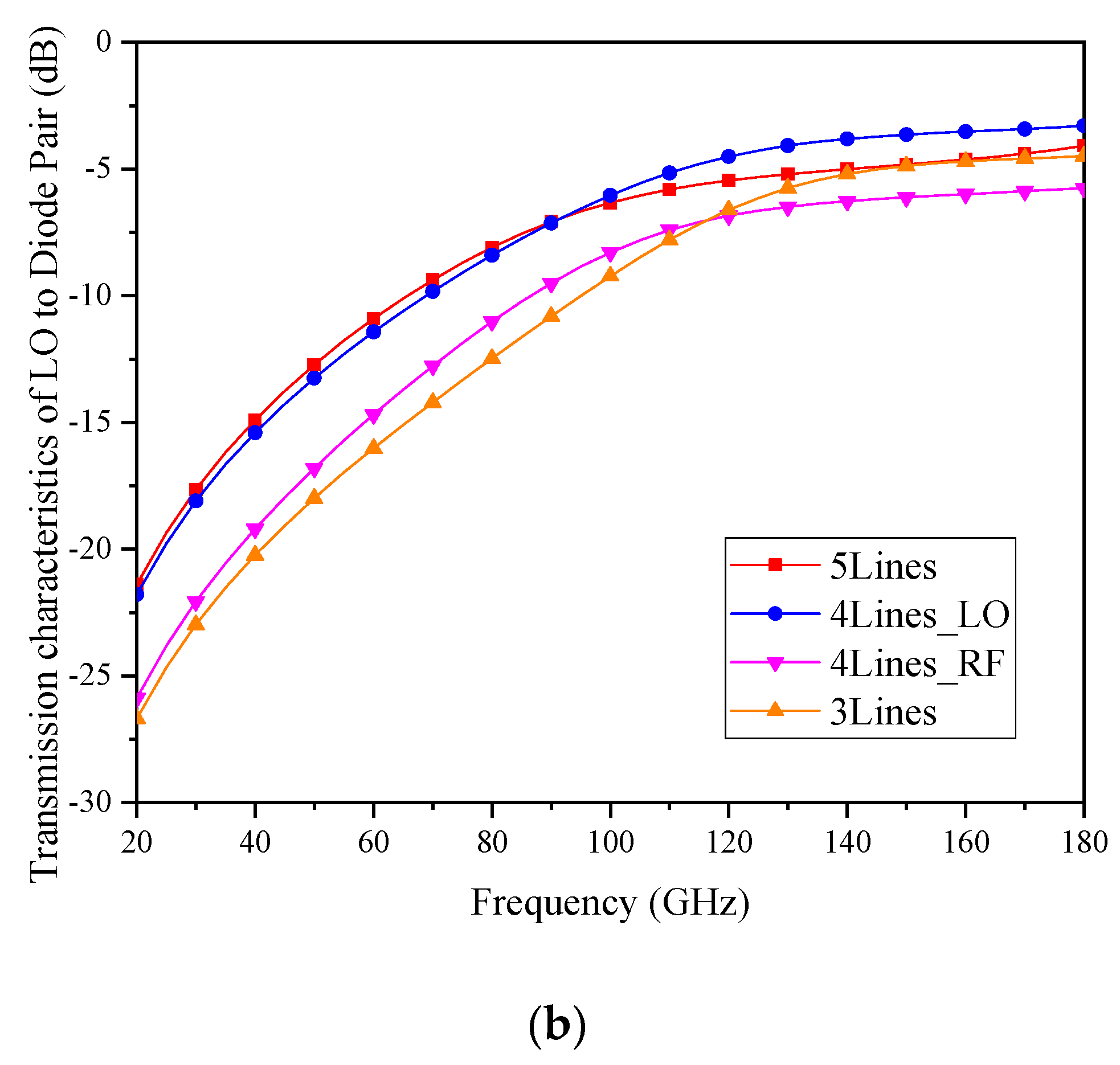
Figure 4.
The simulated conversion gain of (a) different couplers and (b) different spacing.

Figure 5.
The schematic of the present APDP-based sub-harmonic mixer.
Figure 6.
Microscope photograph of the sub-harmonic mixer chip.

Figure 7.
Measurement diagram of the sub-harmonic mixer chip.

Figure 8.
Measured and simulated conversion gains vs. LO power.
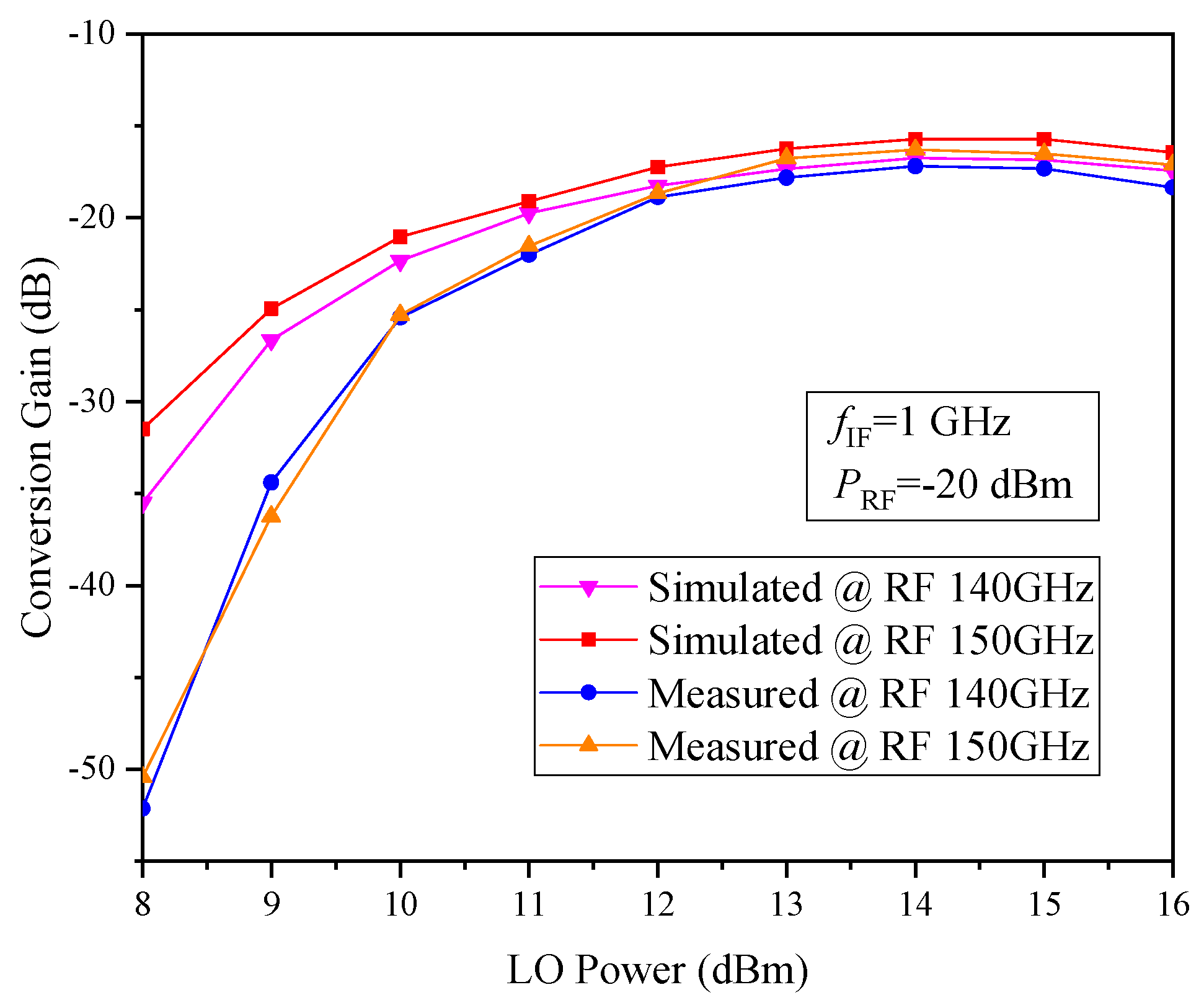
Figure 9.
Measured and simulated conversion gains vs. RF frequency.
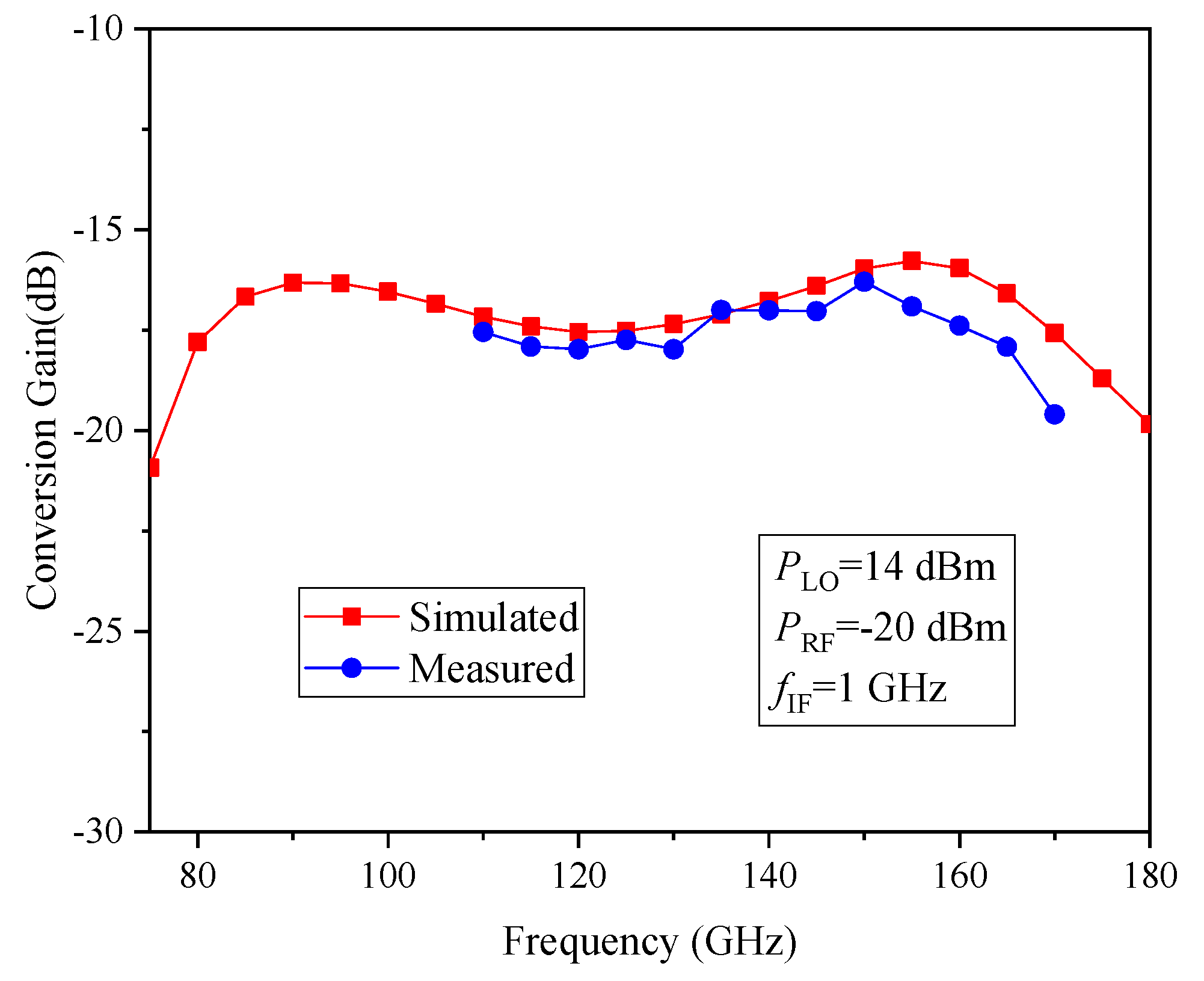
Figure 10.
Measured isolation results vs. RF frequency.
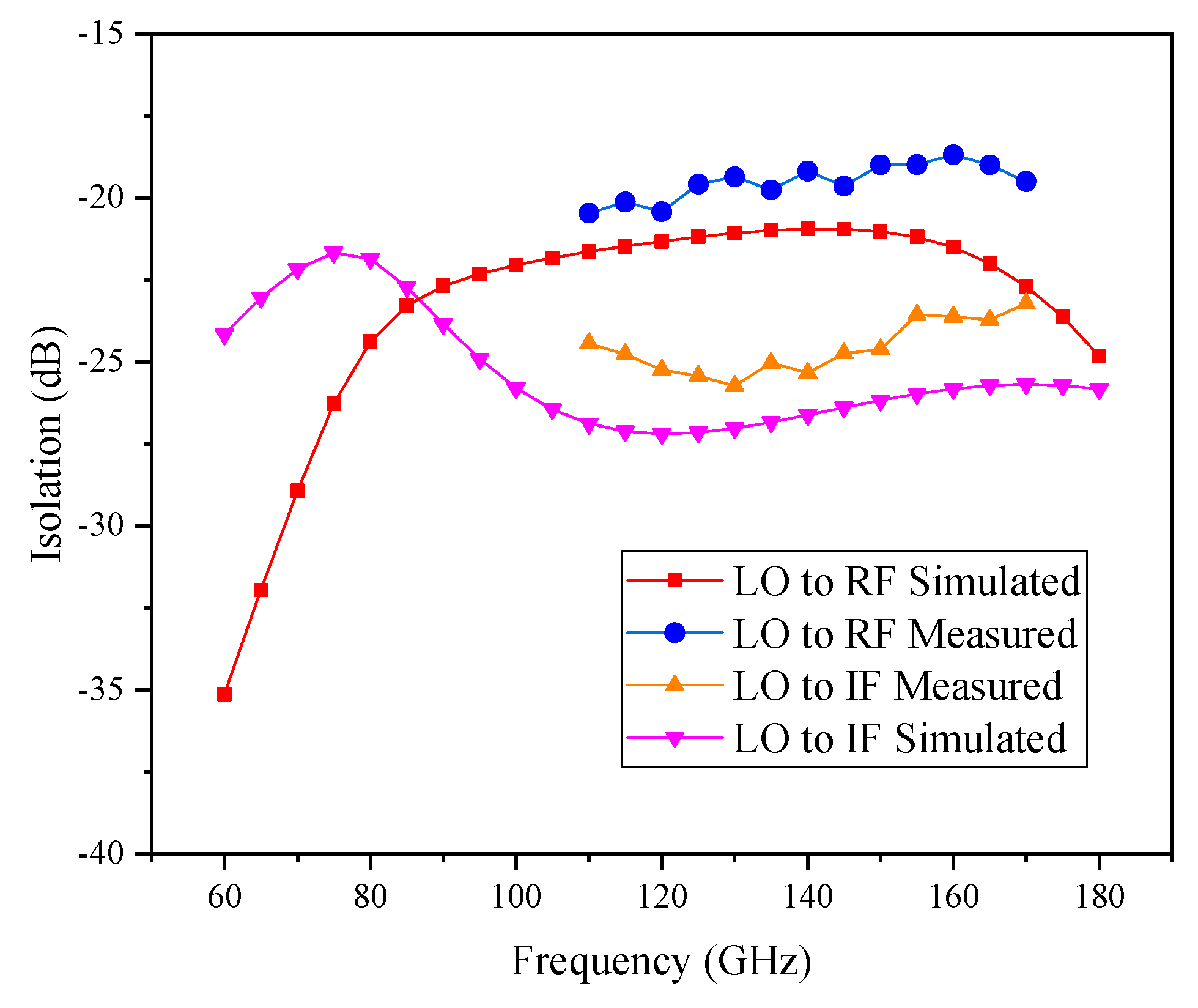
Figure 11.
Measured and simulated conversion gains vs. intermediate frequency (IF).

Table 1.
The parameters of the coupler.
| W1 | W2 | W3 | W4 | W5 |
|---|---|---|---|---|
| 12 μm | 10 μm | 18 μm | 10 μm | 14 μm |
| S1 | S2 | S3 | S4 | L |
| 4 μm | 3 μm | 7 μm | 7 μm | 130 μm |
Table 2.
Measured performances of the passive sub-harmonic mixer MMIC above 100 GHz.
| Ref. | Topology | Process | Device | Conversion Gain (dB) | RF Frequency (GHz) | LO Power (dBm) | Bandwidth (GHz) | Chip Size (mm2) | FOM1 | FOM2 |
|---|---|---|---|---|---|---|---|---|---|---|
| [8] | 2nd | GaAs | Diode | –12.7 to –16.5 | 200–215 | 8 | 15 | 1.25 × 2.95 | 5.41 | 3.57 |
| [9] | 2nd | 0.15 μm GaAs pHEMT | Diode | –10 to –14 | 78–114 | 10 | 36 | 1.5 × 2.0 | 10.56 | 9.06 |
| [10] | 2nd | 80 nm InP HEMT | Diode | –15 to –30 | 165–187 | 13 | 22 | 1.1 × 1.4 | 5.92 | 5.15 |
| [11] | 4th | 5 μm GaAs Diode | Diode | –20 to –30 | 180–196 | 18.7 | 16 | NA | 2.04 | NA |
| [12] | 2nd | 0.1 μm InP HEMT | Diode | –14.3 to –20 | 110–120 | 8.2 | 10 | 1.7 × 2.0 | 2.85 | 1.15 |
| [13] | 4nd | 0.15 μm GaAs pHEMT | Diode | –25.5 to –30 | 100–120 | 15 | 20 | 1.0 × 1.0 | 0.26 | –0.24 |
| [14] | 2nd | 70 nm GaAs mHEMT | 3μm Diode | –14 to –17 | 110–140 | 9 | 30 | 0.82 × 0.66 | 7.77 | 7.50 |
| [15] | 2nd | 0.13 μm SiGe BiCMOS | Diode | –6 to –7 | 100–120 | 16 | 20 | 0.43 × 0.78 | 10.01 | 9.84 |
| [16] | 2nd | 0.13 μm SiGe BiCMOS | Diode | −8 | 122 | 5 | NA | 0.6 | NA | NA |
| [17] | 2nd | 70 nm GaAs mHEMT | 3μm Diode | –13.9 to –17.5 | 110–145 | 14 | 32 | 0.5 × 0.68 | 8.10 | 7.93 |
| [18] | 4nd (Res.) | 0.15 μm GaAs pHEMT | HEMT | –26 to –30 | 176–186 | 18 | 10 | NA | –3 | NA |
| [19] | 2nd (Res.) | 0.1 μm GaAs mHEMT | HEMT | –14 to –17 | 120–150 | 0 | 30 | 1.0 × 0.9 | 7.77 | 7.32 |
| [20] | 2nd (Res.) | 0.1 μm GaAs mHEMT | HEMT | –12.5 to –16 | 120–150 | 4 | 30 | 1.2 × 1.5 | 8.52 | 7.62 |
| [21] | 2nd (Res.) | 0.1 μm GaAs mHEMT | HEMT | –19 to –28 | 180–220 | 2 | 40 | 1.0 × 2.0 | 6.52 | 5.52 |
| –18.5 to –29 | 200–220 | 2 | 20 | 1.0 × 1.8 | 3.76 | 2.86 | ||||
| [22] | 2nd (Res.) | 50 nm InP HEMT | HEMT | –15.5 to –25 | 180–220 | 3 | 40 | NA | 8.27 | NA |
| HEMT | –16.5 to –22 | 200–220 | 4 | 20 | 4.76 | NA | ||||
| This work | 2nd | 70 nm GaAs mHEMT | 3μm Diode | –16.2 to –19.6 | 110–170 | 14 | 60 | 0.47 × 0.66 | 9.68 | 9.53 |
| –15.8 to –20 * (Simulated) | 80–180 | 100 | 12.10 | 11.94 |
© 2020 by the authors. Licensee MDPI, Basel, Switzerland. This article is an open access article distributed under the terms and conditions of the Creative Commons Attribution (CC BY) license (http://creativecommons.org/licenses/by/4.0/).
Share and Cite
MDPI and ACS Style
Wen, J.; Zhang, S.; Sun, L. A Compact Broadband Monolithic Sub-Harmonic Mixer Using Multi-Line Coupler. Electronics 2020, 9, 694. https://doi.org/10.3390/electronics9040694
AMA Style
Wen J, Zhang S, Sun L. A Compact Broadband Monolithic Sub-Harmonic Mixer Using Multi-Line Coupler. Electronics. 2020; 9(4):694. https://doi.org/10.3390/electronics9040694
Chicago/Turabian StyleWen, Jincai, Shengzhou Zhang, and Lingling Sun. 2020. "A Compact Broadband Monolithic Sub-Harmonic Mixer Using Multi-Line Coupler" Electronics 9, no. 4: 694. https://doi.org/10.3390/electronics9040694
Note that from the first issue of 2016, this journal uses article numbers instead of page numbers. See further details here.