Layout Strengthening the ESD Performance for High-Voltage N-Channel Lateral Diffused MOSFETs


Department of Electronic Engineering, National United University, Miaoli City 36003, Taiwan
*
Author to whom correspondence should be addressed.
Electronics 2020, 9(5), 718; https://doi.org/10.3390/electronics9050718
Submission received: 12 April 2020
/
Revised: 25 April 2020
/
Accepted: 26 April 2020
/
Published: 27 April 2020
(This article belongs to the Special Issue Intelligent Electronic Devices)
Abstract
:An electrostatic discharge (ESD) event can negatively affect the reliability of integrated circuits. Therefore, improving on ESD immunity in high-voltage (HV) n-channel (n) lateral diffused metal–oxide–semiconductor field-effect transistor (HV nLDMOS) components through drain-side layout engineering was studied. This involved adjusting the operating voltage, improving the non-uniform turned-on phenomenon, and examining the effects of embedded-device structures on ESD. All proposed architectures for improving ESD immunity in this work were measured and evaluated using a transmission-line pulse system. The corresponding trigger voltage (Vt1), holding voltage (Vh) and secondary breakdown current (It2) results of the tested devices were obtained. This paper first addresses the drift-region length modulation to design different operating voltages, which decreased as the drift region length and shallow trench isolation (STI) length shrunk. When an HV nLDMOS device decreased to the shortest drift region length, the Vt1 and Vh values were closest to 21.85, and 9.27 V, respectively. The It2 value of a low-voltage operated device could be increased to a maximum value of 3.25 A. For the channel width modulation, increasing the layout finger number of an HV LDMOS device did not really help the ESD immunity that because it may suffer the problem of non-uniform turned-on phenomenon. Therefore, adjusting the optimized channel width was the best one method of improvement. Furthermore, to improve the low ESD reliability problem of nLDMOS devices, two structures were used to improve the ESD capability. The first was a drain side—embedded silicon-controlled rectifier (SCR). Here, the SCR PNP-arranged type in the drain side had the best ESD capability because the SCR path was short and had been prior to triggering; however, it also has a latch-up risk and low Vh characteristic. By removing the entire heavily doped drain-side N+ region, the equivalent series resistance in the drain region was increased, so that the It2 performance could be increased from 2.29 A to 3.98 A in the structure of a fully embedded drain-side Schottky diode. This component still has sufficiently high Vh behaviour. Therefore, embedding a full Schottky-diode into an HV nLDMOS in the drain side was the best method and was efficient for improving the ESD/Latch-up abilities of the device. The figure of merit (FOM) of ESD, Latch-up, and cell area considerations improved to approximately 80.86%.
1. Introduction
As semiconductor technology progresses, the functions and efficiency of integrated circuits (ICs) have greatly improved, and microelectronic circuits and power technologies are receiving more attention. In recent years, many electronic manufactures have been designing intelligent products, smart power systems, intelligent vehicles, and Internet of things (IoTs) applications [1,2,3,4,5,6,7,8,9]. Among these, electrostatic discharge (ESD) damage remains a serious problem in high-voltage (HV) units. However, IC applications for HV power conversion must remain highly reliable.
Lateral diffused metal–oxide–semiconductor field-effect transistor (LDMOS) devices have been efficiently applied to ICs for power electronics, power managements and display driver, given their advantages of low ON-resistance and ability to withstand high operating voltages [10,11,12,13,14,15,16]. Therefore, design methods for each operating voltage devices to develop various HV and low-voltage devices by using single-process chips are crucial for many applications. The ESD immunity of devices, under different operating voltages, is worthy of investigation. Furthermore, LDMOS devices may act as HV devices and ESD protection device simultaneously. To reduce the effects of ESD, improving the self-protection performance of HV devices is significant [17,18,19,20,21,22,23,24,25,26,27,28]. Therefore, to achieve good ESD capability in devices, parameters including trigger voltage (Vt1), holding voltage (Vh), and secondary breakdown current (It2) are critical. Theoretically, the It2 value of devices is a standard evaluation for defining the ESD capability and should have a sufficient It2 value for a device to withstand high ESD currents. Therefore, the human-body model (HBM) ESD capability of a component is actually closely related to the It2 measurement value of the component. However, the holding voltage value must be high enough to avoid the latch-up (LU) problem.
In this study, the operating voltage of a device was adjusted by varying the drift-region length (shallow trench isolation [STI] or drift region modulation) to conveniently form various n- channel (n) LDMOS (nLDMOS) devices operating under different operating voltages. Unfortunately, the ability of discharging ESD current remains affected by the non-uniform turned-on phenomenon for the multi-finger layout type, which easily weakens the immunity level per unit device width from ESD particularly for HV LDMOS devices [29,30,31]. Therefore, after confirming the length effect of the drift region, the total channel width and finger number of an MOSFET should be adjusted to clearly understand the non-uniform turned-on problem in the benchmark (reference) nLDMOS device. Then, strengthening the ESD capabilities of an HV LDMOS through drain-side device engineering is necessary. Some improvement techniques embed a silicon-controlled rectifier (SCR) to improve the discharge capability. However, this may cause an LU effect because of its very low holding voltage [32,33,34,35,36]. Therefore, this study evaluated the effect of different parasitic SCR paths on the ESD immunity of LDMOS related devices. The last part of the study involved removing the heavily doped N+ region to embed a parasitic Schottky diode into the drain side of an HV nDLMOS. The series resistance characteristics of embedded Schottky diodes in the drain side indicated that this method can effectively increase the It2 value (ESD reliability) of HV nLDMOS devices.
2. Cell Design of the HV nLDMOSs
2.1. HV nLDMOS Reference Device
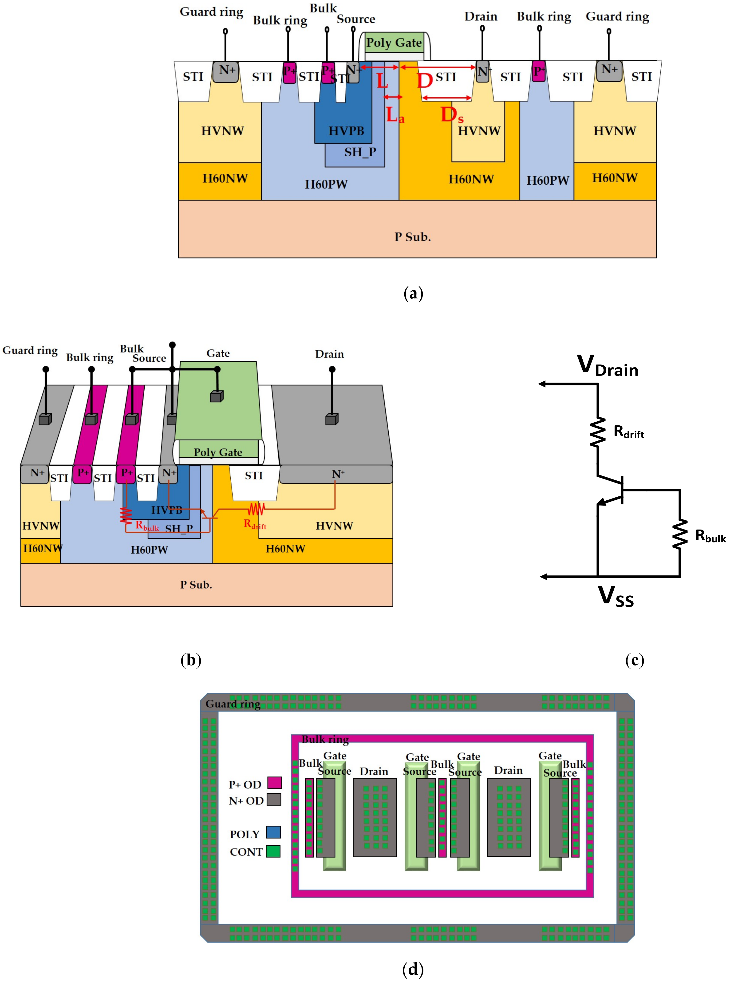
Generally, nLDMOS devices are operated in an HV environment for many applications. Therefore, this paper focuses on the physical-parameter optimization and ESD capability enhancement studies for HV nLDMOS devices. All samples of HV nLDMOS related devices were fabricated using a Taiwan Semiconductor Manufacturing Company (TSMC) 0.25 μm HV Bipolar-Complementary metal-oxide-semiconductor-Double-diffused MOSFET (BCD) standard process with a gate-grounded nMOSFET (GGnMOS) configuration. Figure 1a displays a cross-sectional view of the HV nLDMOS Reference device, which has a long drift-region length D and STI isolation length Ds. The breakdown voltage (VBK) of the nLDMOS device exhibited a higher HV performance as the large drift region resistance (Rdrift) can suppress the high electric field concentrated at the gate edge and extend the length of depletion region. Moreover, the length of La in H60PW layer, which is below the gate electrode, could be adjusted to increase the channel length L and affect channel resistance. Figure 1b presents a three-dimensional (3D) structure view of the HV nLDMOS Reference device. When an MOSFET transistor under the configuration of a gate-grounded electrode forms a GGnMOS structure, it can discharge the ESD surge current through the parasitic bipolar-junction transistor (BJT) underneath. This device can release ESD current through the drain side N+, HV N-well, drift region H60NW, H60PW, SH_P, HVPB, and source side N+ as the ESD current enters the device. Based on the device structure, the equivalent circuit of the nLDMOS Reference device is shown in Figure 1c; Rbulk is the parasitic resistances of the source-to-bulk; the parasitic resistance (Rdrift) in the drift region is sufficiently high, as compared with a conventional CMOS MOSFET. In this paper, various types of HV nLDMOS devices are designed with the multi-fingers layout. The total finger number is four (except for in Section 2.3), each channel length (L) is varied, the channel width is 75 μm (except for in Section 2.3), and STI length in the drain side is 12.83 μm. The layout view of the nLDMOS Reference device is presented in Figure 1d.
2.2. HV nLDMOS DUTs with Drift Region Modulation (Operating Voltage Modulation)
As detailed in this subsection, the drain-side STI region (i.e., the STI length Ds) of the nLDMOS Reference device was shrunk. Figure 2a,b illustrate the 3D structure and layout view of an HV nLDMOS device with drift region modulation at the lowest voltage (shrunk to the shortest STI = 0 μm) usage. Due to thesufficiently long Ds, the nLDMOS Reference device could disperse a high electric field that focused on the gate edges and extended the depletion region for operation in HV situations. Therefore, drift region STI distance Ds was adjusted to achieve drift region modulation (which also shrinks the length D). The Ds distance reduced by a quarter from the original Reference device Ds (12.83 μm) in order, which were 9.63 μm (STI 3/4), 6.43 μm (STI 2/4), 3.23 μm (STI 1/4), and finally to the shortest 0 μm (STI 0) with the structure of the shortest length in the drift region, respectively. These devices were designed to effectively reduce the extended depletion region and drift resistance (Rdrift) shown in Figure 1c, and these HV nLDMOS devices were estimated to be able to be appropriately adjusted for many voltage operations. Thus, their corresponding ESD reliability capabilities should be evaluated to discharge transient current through this process.
2.3. HV nLDMOS DUTs with Channel Width Modulation
To improve the withstand voltage and ESD immunity of an HV device, the layout ways need to be well-planned. For efficient manufacturing an HV semiconductor MOSFET device, it generally designed with a large channel width and multifinger layout manner. However, the issue of non-uniform turned-on phenomenon is always a serious problem in HV GGnMOS devices, because a multi-finger structure cannot fully turn on in each MOSFET, causing the ESD capability to be very weak per unit channel-width of ESD. Therefore, it seems to be no way to effectively protect a transient ESD current by this large cell-area HV nLDMOS.
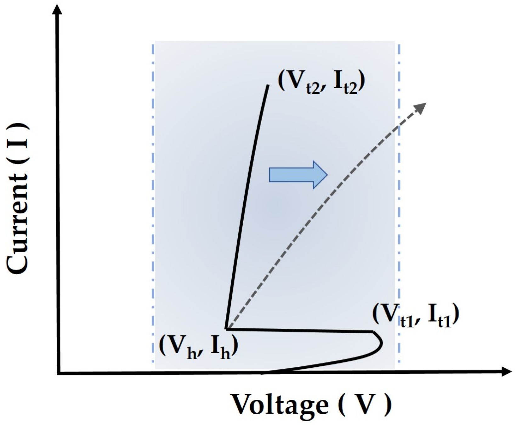
The Rbulk resistance of each finger shown in Figure 1b and Figure 2a of a GGnMOS ESD device by the multi-finger structure will have a slight difference in manufacturing process. However, each finger of an nLDMOS device is independent and any one finger with the largest Rbulk on-resistance will be the first one to turn on, where an ESD pulse occurred, this finger would easily reach the secondary breakdown. If the other fingers have not been triggered to turn on instantly, this nLDMOS device may reach the melting point to cause device failure. Eventually, the ESD immunity of this protection device becomes not proportional to the device size. As shown the voltage-current characteristic curve of a protection device in Figure 3, the difference between the secondary breakdown voltage (Vt2) and Vt1 values affects the turned-on probability and non-uniform turned-on issues on each MOSFET [24]. In order to enhance uniform conduction, it is generally desirable to adjust the snapback curve as shown by the dashed curve in Figure 3. Therefore, the next sub-section further purposes a drain-side embedded SCR structure to improve the ESD capability. This new added SCR can have a very strong capability of ESD that can be applied in high voltage applications. However, it also has some disadvantages, which includes a very low Vh value. In this sub-section, the finger number and channel-width effects of multi-finger nLDMOS devices will be evaluated for the issue of non-uniform turned-on problem. Then, the La length is adjusted and makes the channel length L= 2.75 μm in this nLDMOS Reference device. Figure 4a is a two-fingers (M = 2) structure with each channel width being 75 μm and the drain region sharing. Meanwhile, it will be used to compare the ESD capability between the two-finger and four-finger structures. Furthermore, Figure 4b was extended each channel width of Figure 4a to 150 μm, and its ESD capability will be compared with the device of Figure 1d (M = 4 and same total channel width).
2.4. HV nLDMOS DUTs with Embedded SCR Modulation
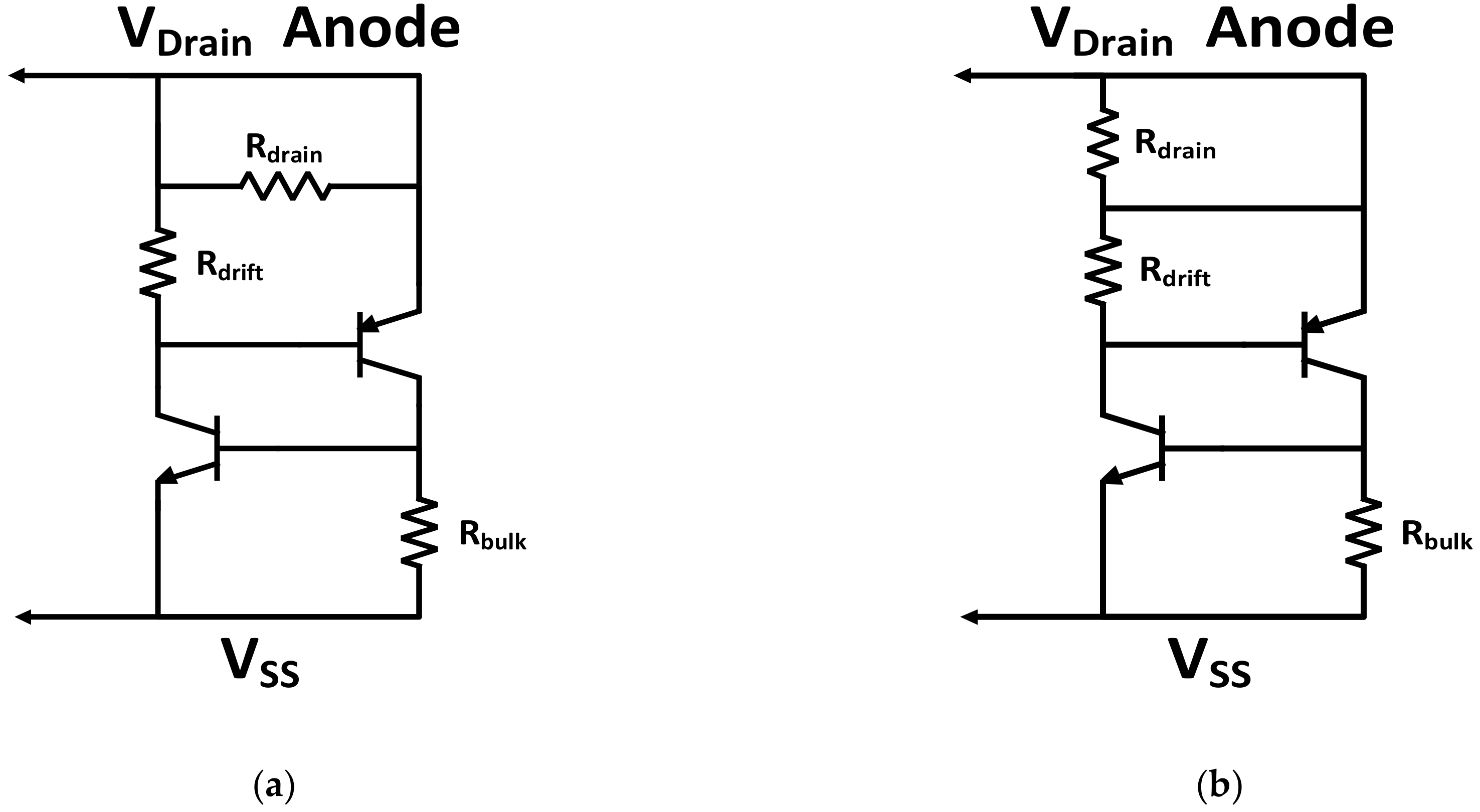
A silicon-controlled rectifier (SCR) is often applied in power electronics or as an ESD protection device as it has a strong capability in discharging transient current. In order to improve the ESD reliability of an nLDMOS, which has the serious problems, including non-uniform turned-on issue and low ESD capability in the multi-finger structure. Therefore, one idea based on the nLDMOS Reference device, a parasitic SCR element (by embedded a P+ zone) can be built into the drain side. An HV nLDMOS with the drain side NPN-arranged type and PNP-arranged type for ESD dissipation. It means that these embedded SCRs may achieve the result of improving ESD capability on the nLDMOS Reference device. Figure 5 shows some layout structures, which are divided the drain region into three or five equal partitions and regularly embedded P+ zones to form four different embedded SCR arrangements. Figure 5a,c are the SCR embedded structures of NPN- and NPNPN-arranged types, which indicates that the SCR path is inner and longer to the drain electrode. On the contrary, Figure 5b,d are the SCR embedded structures of PNP and PNPNP-arranged types, and the SCR paths are outer and shortest to the both side of the drain electrode. Figure 6 shows the parasitic equivalent circuits of an nLDMOS with drain-side NPN- and PNP-arranged types. The main difference between these two circuits is the location of the P+ implants of an SCR anode. Meanwhile, the drain end Rdrain is sufficiently high and cannot be neglected for these NPN- and PNP-arranged types. Similarly, the equivalent circuit situations of Figure 6 also occur for the drain-side PNPNP-arranged type and NPNPN-arranged type. Therefore, the major ESD discharging path will be varied and depended on these embedded SCRs locations. Eventually, they will affect the ability of nLDMOS-SCR related devices to withstand ESD surges.
2.5. HV nLDMOS DUTs with Embedded Schottky-Diode Modulation
As mentioned previously, an nLDMOS device has the non-uniform turned-on problem as with a multi-finger layout. However, this component still need to have a perfect capability of self-protection when it acts as a protection device in integrated circuits, it means that this nLDMOS transistor need to have a good ESD dissipation capability. Therefore, in this sub-section, another reinforced structure which explored for purposes of increasing It2 level to improve the self-protection capability. The channel length of nLDMOS Reference device here is L = 2 μm. In order to improve the ability to discharge ESD current per unit area on the nLDMOS Reference device, the implants of heavily doped N+ layer in the drain side were removed, which made this device forming an equivalent series Schottky-diode by silicide and HVNW lightly-doped layer in the drain region. Therefore, the nLDMOS Reference device is changed and embedded a series Schottky diode in the current-conduction path. Figure 7a shows a 3D structure of full removing the entire drain side heavily-doped N+ layer, it can be regarded as the original current discharging path with an embedded Schottky diode beneath the drain electrode. Thus, a heavily-doped N+ ring around the central Schottky diode to form a structure of nLDMOS parallel with an embedded Schottky diode shown in Figure 7b. Different drain-side area ratios of the Schottky diode by periphery heavily-doped N+ region is modulated, which is used to evaluate the ESD-capability influence upon the embedded different area ratio of Schottky diode at the drain side. Finally, the area ratio of heavily-doped N+ versus Schottky diode region is shown in Table 1. Meanwhile, the parasitic equivalent circuits of an nLDMOS with drain-side full removing N+ heavy doping and a central-type embedded Schottky diode modulation in the drain side are shown in Figure 8, respectively.
3. Experimental Testing Systems
A measurement instrument of transmission-line pulse (TLP) system was used in this paper which is used to simulate the human-body model (HBM) of a transient waveform from an ESD event into a device and which is widely exercised to measure the ESD capability of protection devices. Furthermore, this system can generate a square wave with 100 ns short pulse width and has a short rising/falling time less than 10 ns, and the voltage-current characteristics including the trigger voltage (Vt1), holding voltage(Vh) and secondary breakdown current(It2) on the devices under test (DUTs) can be tested. Therefore, from these important physical extracted parameters, the capability of ESD immunity of these DUTs can be easily determined. Meanwhile, the breakdown-voltage measurement of a device is executed by a semiconductor parameter analyzer.
4. Experimental Results
4.1. ESD Capability of HV nLDMOS DUTs with Drift-Region Modulation (Operating-Voltage Modulation)
HV nLDMOSs of the Reference device and drift-region modulation devices were measured by a TLP testing machine, all of measurement results and important physical extracted parameters are presented in Figure 9 and Table 2. Then, it can be found that as the length of the drift region is reduced, the Rdrift resistance of the drift region shown in Figure 1c on a DUT will be decreased accordingly. Therefore, the DUT of STI0 would have properties for the lowest operating voltage, and the junction breakdown voltage (Vbk) would be decreased to the lowest voltage being 11.12 V. In Figure 10 (the Vt1 and Vh distribution curves), because of reducing the length of STI region which will make the Vt1 having a significant downward trend due to a decreasing of the equivalent series resistance Rdrift. Although the Vh value has a little rising while shrinking the STI length by 1/4, however it will have a significant reduction as the STI length being decreased and then the series resistance decreased too. In addition, the It2 value has a slightly decreasing by reducing the drift region length at the first and second adjustments, but the It2 abilities of the DUTs will also obviously increase after it continues to shrink which even promoted larger than the nLDMOS Reference device. This is also due to a decreasing of the series resistance and power consumption in the drift region, then the It2 distribution curve is shown in Figure 11. Moreover, when the drift region was shrinked to the shortest (STI0) DUT, the Vt1 and Vh values were become to the lowest 21.85 V and 9.27 V, respectively. In other words, as the STI length is shrunk to 0, the STI zone in the drain side will be completely disappeared; the difference gap between Vt1 and Vh values is smaller accordingly shown in Table 2. Then, the phenomenon of non-uniform turned-on of this new device has been slight which made the It2 value (STI0) has the largest value being 3.25 A, and it can be effectively applied to a low operating voltage situation. Moreover, the figure of merit (FOM) of the ESD, LU, and cell area considerations are defined as (It2 × Vh)/Cell-area. Then, the FOM value of the STI_3/4 DUT has highest performance being 3045.68 μA × V/μm2 in this modulation.
4.2. ESD Capability of HV nLDMOS DUTs with Channel-width Modulation
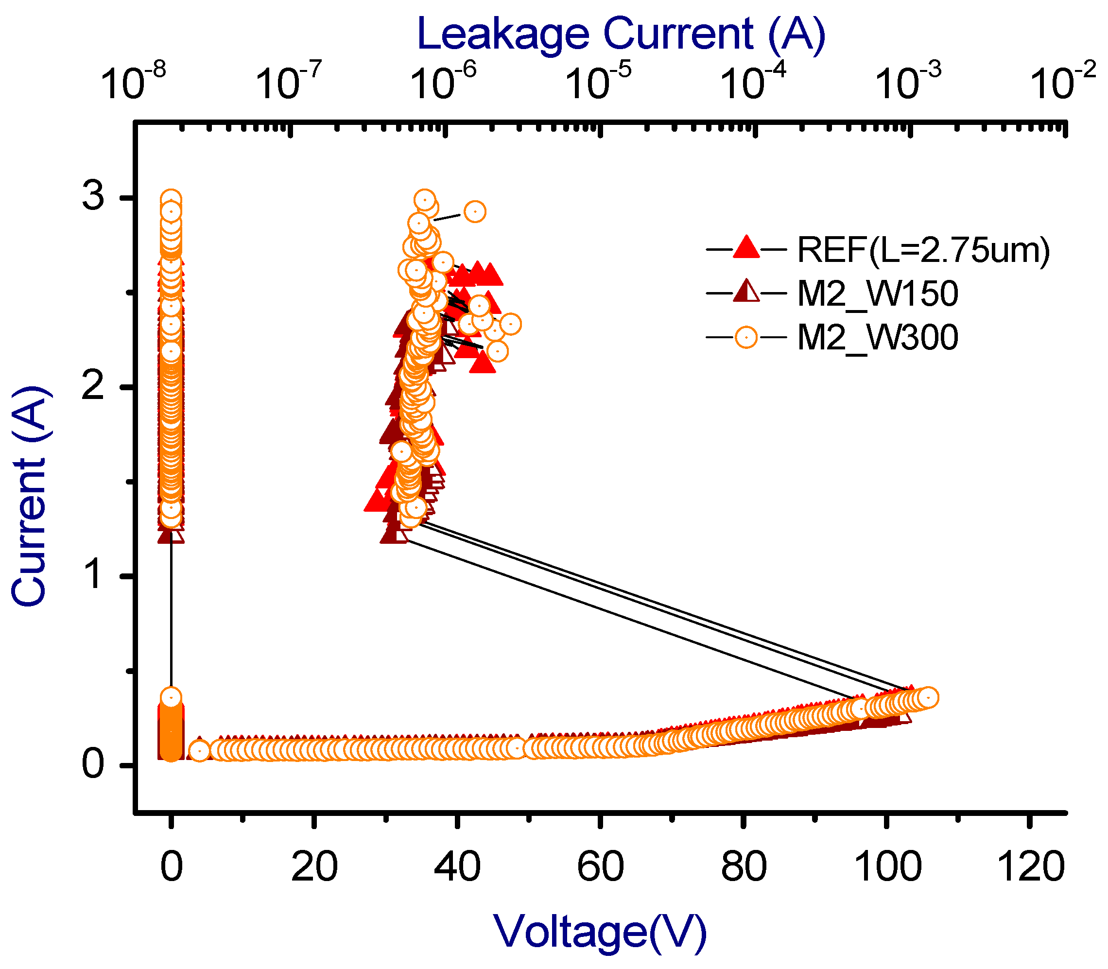
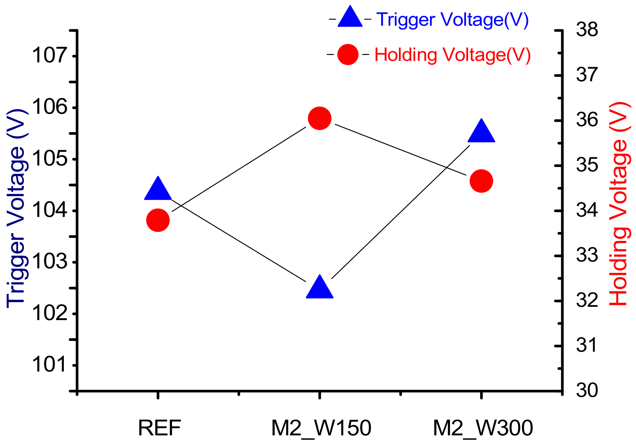
Measurement results of HV nLDMOS devices with the channel-width modulation are shown in Figure 12 and Table 3. Meanwhile, the corresponding important physical-extracted parameters of snapback Vt1/Vh and It2 data are shown in Figure 13 and Figure 14. When the channel length (L) of the nLDMOS Reference device in this sub-section decreased as the H60PW layer shrunk, which was reduced from 3 μm of the Reference device in the previous sub-section to 2.75 μm. The lower channel resistance caused higher ESD surge current, which reduced the It2 value from 2.79 A to 2.5 A in this new HV nLDMOS Reference device. Furthermore, it can be found that by adjusting the finger number M = 2 and then total channel width is 150 μm of this nLDMOS (M2_W150) device, the It2 value has slightly decreased to 2.45 A as compared with the M= 4 and total channel width is 300 μm of the nLDMOS Reference (M4_W300) device. However, because of the HV nLDMOS DUT in M= 4 (M4_W300) has a serious non-uniform turned-on phenomenon by a multi-finger structure which is severely limited the capability of discharging ESD current. Next, by increasing the total channel width of M2_W150 from 150 μm to 300 μm which is named as the M2_W300. Then, the It2 value of M2_W300 can be greatly increased to 2.73 A. As the M2_W300 (M = 2) device compared with the same total channel width DUT of the M4_W300 (M = 4) device, the ESD capability of M2_W300 has indeed improved. In other words, the DUT of M4_W300 whose probability was higher on the first turned-on finger easily reached the failure point before others fingers of this MOSFET turned-on as compared with the DUT of M2_W300. Moreover, in the FOM consideration, the M2_150 is best in this modulation being FOM = 4691.63 μA × V/μm2. However, the designing of fingers number and channel-width manner in the circuit design are affected by the free space that the I/O cell area can be used. Therefore, how to improve the capability of non-uniform turned-on in a multi-finger structure for the HV nLDMOS device is a very important subject.
4.3. ESD Capability of HV nLDMOS DUTs with Embedded SCR Modulation
Measurement data of HV nLDMOS devices with the embedded SCR modulation are presented in Figure 15 and Table 4. From Figure 5a,c and Figure 6a, it can be found that the SCRs (P+ stripes) of the nLDMOS-SCR NPN and NPNPN-arranged types were embedded in the drain region far away from the gate, the parasitic BJT of LDMOS (N+ stripe) was the first one to turn on when an ESD surge current entered. After the ESD surge voltage increased enough (as an ESD current passed through Rdrain and Rdrift) to trigger these embedded SCRs, these components can partially discharge the ESD current through the parallel path of SCRs. As the characteristics of nLDMOS are more obvious, their Vt1 values will be higher. Of course, Vh values of these components can maintain higher performance. However, in Figure 5b,d, and Figure 6b, if the SCRs (P+ stripes) of an nLDMOS were embedded in the both side of drain region which are more nearer the poly-gate like the nLDMOS-SCR PNP and SCR PNPNP-arranged structures do, then they have higher ESD dissipation capability. When an ESD event occurred, these structures of nLDMOS-SCR PNP- and SCR PNPNP-arranged types just require lower voltage (as an ESD current passed through Rdrift) to trigger SCRs under the conductive path, it is due to the P+ zone in the drain side being closer the gate. It made the Vt1 values of these structures having the lower values of 103.66 V, and 103.98 V, respectively, as compared with others DUTs, which included the nLDMOS Reference device. In addition, because of they have notable SCR characteristics; the corresponding Vh values will be decreased. Obviously, it can discharge larger ESD current by the path of embedded SCRs. Therefore, the It2 data have the best improvement from 2.5 A to 4.96 A and 4.44 A, respectively, for the nLDMOS-SCR PNP and PNPNP-arranged components. As for the nLDMOS-SCR PNP -arranged, it has a larger area of P+ zone on the both side of drain, the FOM of this ESD protection device can be upgraded from 2831.83 μA × V/μm2 to 4255.51 μA × V/μm2 (50.27% improvement). Finally, the corresponding Vt1, Vh and It2 values of the nLDMOS related devices by embedded different SCRs arrangements are shown in Figure 16 and Figure 17.
4.4. ESD Capability of HV nLDMOS DUTs with Embedded Schottky-Diode Modulation
Measurement results of HV nLDMOS devices with the embedded Schottky-diode modulation are shown in Figure 18 and Table 5. The channel length L of this nLDMOS Reference device was set to be 2 μm, the It2 value of this Ref. device is significantly decreased to 2.29 A due to the channel-length reduction. However, the It2 level could be effectively promoted by adding an embedded Schottky diode in the drain side. In other words, after removing the entire heavily doped N+ layer in the drain side, the It2 value of this device has higher performance than that of other DUTs. It is equivalent to serializing the Schottky diode in the drain end shown in Figure 8a, it has higher impedance when an ESD transient entered the drain electrode. Therefore, this new architecture made the Vt1 value therefore increasing to 109.43 V, and the It2 value of this device can be increased from 2.29 A for the Reference device (L = 2 μm) to 3.98 A (73.8% improvement). Meanwhile, the FOM value can be improved from 2400.38 μA/μm2 to 4341.27 μA × V/μm2 (80.86% improvement as compared with the Ref. device). Furthermore, it has a higher Vh value as compared with the nLDMOS-SCR PNP-arranged type structure in the previous sub-section. Finally, the Vt1, Vh and It2 distribution charts about the embedded Schottky-diode related components are shown Figure 19 and Figure 20. These experimental results revealed that the Vt1 and It2 values have a decreasing trend when the area ratio of Schottky diode decreased (more like the original nLDMOS Reference device). To explain simply, if the area ratio of this parasitic Schottky diode is small, the characteristic of equivalent series Schottky diode will be not apparent (the Rdrain more higher shown in Figure 8b), which causes the Vt1 and It2 values, corresponding to these devices decreased accordingly. The relevant area ratio of embedded Schottky diode of this modulation can refer to Table 1. Overall, this new architecture (embedded a Schottky diode in the drain) has the most positive impact (80.86% ↑) on the FOM, compared with previous three techniques shown in Table 6.
5. TCAD Simulation and Verification
For verification of ESD-reliability improvement by this novel embedded Schottky-diode in the LDMOS device drain side, the Silvaco EDA software was used to simulate a 2D total current density and lattice-temperature distributions with embedded Schottky-diode variations. Figure 21 and Figure 22 are the diagrams of total current density and lattice temperature of these related devices at the drain-current Id = 1 × 10⁻⁴ A injecting condition. From these diagrams, the high current density and lattice temperature are obviously concentrated near the drain side and below the STI region. In the Figure 21a and Figure 22a, the structure of nLDMOS Reference device which had the highest current density and lattice temperature being 1.5 × 10⁻³ (A/cm2), and 693 (K), respectively. On the contrary, in the Figure 21b and Figure 22b, the structure of removing entire drain-side heavily N+ zone which has the maximum series resistance by embedded a 100% area of Schottky diode in drain side, then the total current density and lattice temperature could be reduced to 1.15 × 10⁻³ (A/cm2), and 684(K), respectively. It made this nLDMOS component can withstand higher ESD current (current density) and it is not easily concentrated to reach the melting point to damage. Finally, the Schottky_SUR1, Schottky_SUR2, and Schottky_SUR3 samples with different area ratios of embedded Schottky diode in the drain side are shown in Figure 21c–e and Figure 22c–e. It can be found that an nLDMOS device would have higher current density and lattice temperature as with fewer Schottky-diode area ratio at the drain side. Therefore, it can be concluded that it is an easy and effective technique to increase the ESD withstanding capability for an HV nLDMOS with a drain-side embedded Schottky diode.
6. Conclusions
This research paper is divided into four parts focussed on promoting the ESD immunity of HV nLDMOS devices. The first part focuses on the effect of drift region modulation and the corresponding ESD immunity of these related devices. As the length of the drift region decreased, the operating voltage directly decreased from reduced equivalent series resistance. Therefore, for the with the shortest distance (STI0), the Vt1 and Vh values decreased from 104.47 V to 21.85 V and 32.53 V to 9.27 V from those of the nLDMOS Reference device, respectively. Then, protection devices were conveniently designed for high and low operating voltages in a single chip and improved the It2 value from 2.79 A to 3.25 A (and saved the layout area). The second part revealed that, for improved the ESD immunity per unit area of an HV LDMOS device, shortening the channel width and enlarging the finger number are not optimal strategies within the same layout area. An optimized channel width from fine adjustment is the best method for improvement of ESD immunity. In third part, to alleviate the problem of non-uniform turned-on of protection devices, the embedded SCR PNP-arranged type in the drain side had the highest ESD current discharge capability, and the FOM data was increased to 4255.51 μA × V/μm2; however, the Vh value decreased to the low value of 25.59 V. Finally, by using an embedded Schottky-diode in the drain side to remove the entire heavy N+-doped zone, the It2 value of this fully embedded Schottky diode in an HV nLDMOS device could be increased from 2.29 A to the largest 3.98 A. The FOM value improved significantly to 4341.27 μA × V/μm2, and the Vh value stayed higher value (32.54 V) than did the embedded SCR PNP-arranged type. Therefore, improving ESD immunity capability (higher It2 value) requires consideration of LU reliability (higher Vh vlaue) and saving the cell layout area (smaller cell area). An HV nLDMOS device embedded with a Schottky diode in the drain side is a favorable improvement strategy. A device with this architecture can consider ESD, LU, and cell-area saving. Therefore, the FOM significantly improved by approximately 80.86% over that of the nLDMOS Reference device.
Author Contributions
Conceptualization, S.-K.F. and S.-L.C.; Data curation, S.-K.F.; Formal analysis, S.-K.F. and S.-L.C.; Funding acquisition, S.-L.C.; Methodology, S.-K.F. and S.-L.C.; Project administration, S.-K.F. and P.-L.L.; Resources, P.-L.L.; Supervision, S.-L.C.; Validation, S.-K.F., S.-L.C. and H.-W.C.; Visualization, H.-W.C.; Writing – original draft, S.-K.F.; Writing – review & editing, S.-L.C. All authors have read and agreed to the published version of the manuscript.
Funding
This research received no external funding.
Acknowledgments
In this work, authors would like to thank the Taiwan Semiconductor Research Institute in Taiwan for providing the process information and fabrication platform. And, authors would like to acknowledge the financial support of the Ministry of Science & Technology of Taiwan.
Conflicts of Interest
The authors declare no conflict of interest.
Abbreviation
| Symbol | Meaning |
| BCD | Bipolar-Complementary metal-oxide-semiconductor-Double-diffused MOSFET |
| BJT | Bipolar-junction transistor |
| DUT | Device under test |
| ESD | Electrostatic discharge |
| FOM | Figure of merit |
| GGnMOS Gate | Grounded nMOSFET |
| HV nLDMOS | High voltage n-channel lateral diffused MOSFET |
| HBM | Human-body model |
| It2 | Secondary breakdown current |
| IC | Integrated circuit |
| IoT | Internet of things |
| LU | Latch-up |
| SCR | Silicon-controlled rectifier |
| STI | Shallow trench isolation |
| TLP | Transmission-line pulse system |
| Vbk | Breakdown voltage |
| Vh | Holding voltage |
| Vt1 | Trigger voltage |
References
- Lee, M.; Uhm, Y.; Kim, Y.; Kim, G.; Park, S. Intelligent power management device with middleware based living pattern learning for power reduction. IEEE Trans. Consum. Electron. 2009, 55, 2081–2089. [Google Scholar] [CrossRef]
- Murphey, Y.; Park, J.; Kiliaris, L.; Kuang, M.; Masrur, M.; Phillips, A.; Wang, Q. Intelligent Hybrid Vehicle Power Control—Part II: Online Intelligent Energy Management. IEEE Trans. Veh. Technol. 2013, 62, 69–79. [Google Scholar] [CrossRef]
- Vidya, V.; Dharmana, M. Model reference based intelligent control of an active suspension system for vehicles. In Proceedings of the International Conference on Circuit, Power and Computing Technologies, Kollam, India, 20–21 April 2017; pp. 1–5. [Google Scholar]
- Yang, L. Research on Design of Weak Current Protection Circuit in Intelligent Home Control Circuit under the Background of Internet of Things. In Proceedings of the International Conference on Mechanical, Control and Computer Engineering, Huhhot, China, 14–16 September 2018; pp. 189–191. [Google Scholar]
- Yi, D.; Su, J.; Liu, C.; Chen, W. Trajectory Clustering Aided Personalized Driver Intention Prediction for Intelligent Vehicles. IEEE Trans. Ind. Inf. 2019, 15, 3693–3702. [Google Scholar] [CrossRef] [Green Version]
- Vdovic, H.; Babic, J.; Podobnik, V. Automotive Software in Connected and Autonomous Electric Vehicles: A Review. IEEE Access 2019, 7, 166365–166379. [Google Scholar] [CrossRef]
- Zhongzheng, T.; Yangzi, S.; Silong, W. Design of Power Production Safety Monitoring System Based on Intelligent Internet of Things. In Proceedings of the International Conference on Smart Grid and Electrical Automation, Xiangtan, China, 10–11 August 2019; pp. 73–77. [Google Scholar]
- Lu, T.; Chen, X.; Bai, W. Research on environmental monitoring and control technology based on intelligent Internet of Things perception. J. Eng. 2019, 23, 8946–8950. [Google Scholar] [CrossRef]
- Sun, Z.; Xing, X.; Wang, T.; Lv, Z.; Yan, B. An Optimized Clustering Communication Protocol Based on Intelligent Computing in Information-Centric Internet of Things. IEEE Access 2019, 7, 28238–28249. [Google Scholar] [CrossRef]
- Zhang, Y.; Pendharkar, S.; Hower, P.; Giombanco, S.; Amoroso, A.; Marino, F. A RESURF P-N bimodal LDMOS suitable for high voltage power switching applications. In Proceedings of the International Symposium on Power Semiconductor Devices & IC’s, Hong Kong, China, 10–14 May 2015; pp. 61–64. [Google Scholar]
- Kojima, J.; Matsuda, J.; Kamiyama, M.; Tsukiji, N.; Kobayashi, H. Optimization and analysis of high reliability 30–50 V dual RESURF LDMOS. In Proceedings of the International Conference on Solid-State and Integrated Circuit Technology, Hangzhou, China, 25–28 October 2016; pp. 1–3. [Google Scholar]
- Matsuda, J.; Kuwana, A.; Kojima, J.; Tsukiji, N.; Kobayashi, H. Wide SOA and High Reliability 60–100 V LDMOS Transistors with Low Switching Loss and Low Specific On-Resistance. In Proceedings of the International Conference on Solid-State and Integrated Circuit Technology, Qingdao, China, 31 October–3 November 2018; pp. 1–3. [Google Scholar]
- Zhang, G.; Zhang, W.; He, J.; Zhu, X.; Zhang, S.; Zhao, J.; Zhang, Z.; Qiao, M.; Zhou, X.; Li, Z.; et al. Experiments of a Novel low on-resistance LDMOS with 3-D Floating Vertical Field Plate. In Proceedings of the International Symposium on Power Semiconductor Devices and ICs, Shanghai, China, 19–23 May 2019; pp. 507–510. [Google Scholar]
- Guo, S.; Chen, X. A Novel p-LDMOS Additionally Conducting Electrons by Control ICs. IEEE J. Electron Devices Soc. 2019, 7, 710–716. [Google Scholar] [CrossRef]
- Bhoir, M.; Kaushal, K.; Panda, S.; Singh, A.; Jatana, H.; Mohapatra, N. Source Underlap—A Novel Technique to Improve Safe Operating Area and Output-Conductance in LDMOS Transistors. IEEE Trans. Electron Devices 2019, 66, 4823–4828. [Google Scholar] [CrossRef]
- Wei, Y.; Luo, X.; Ge, W.; Zhao, Z.; Ma, Z.; Wei, J. A Split Triple-Gate Power LDMOS with Improved Static-State and Switching Performance. IEEE Trans. Electron Devices 2019, 66, 2669–2674. [Google Scholar] [CrossRef]
- Duvvury, C.; Carvajal, F.; Jones, C.; Briggs, D. Lateral DMOS design for ESD robustness. In Proceedings of the International Electron Devices Meeting. IEDM Technical Digest, Washington, DC, USA, 10–10 December 1997; pp. 1–4. [Google Scholar]
- Kawamoto, K.; Takahashi, S.; Fujino, S.; Shirakawa, I. A no-snapback LDMOSFET with automotive ESD endurance. IEEE Trans. Electron Devices 2002, 49, 2047–2053. [Google Scholar] [CrossRef]
- Wang, C.; Ker, M. ESD Protection Design with Lateral DMOS Transistor in 40-V BCD Technology. IEEE Trans. Electron Devices 2010, 57, 3395–3404. [Google Scholar] [CrossRef]
- Chen, W.; Ker, M. New Layout Arrangement to Improve ESD Robustness of Large-Array High-Voltage nLDMOS. IEEE Electron Device Lett. 2010, 31, 159–161. [Google Scholar] [CrossRef]
- Chen, W.; Ker, M. Improving Safe Operating Area of nLDMOS Array With Embedded Silicon Controlled Rectifier for ESD Protection in a 24-V BCD Process. IEEE Trans. Electron Devices 2011, 58, 2944–2951. [Google Scholar] [CrossRef]
- Malobabic, S.; Salcedo, J.; Hajjar, J.; Liou, J. NLDMOS ESD Scaling Under Human Metal Model for 40-V Mixed-Signal Applications. IEEE Electron Device Lett. 2012, 33, 1595–1597. [Google Scholar] [CrossRef]
- Ye, R.; Liu, S.; Sun, W.; Su, W.; Lin, F.; Sun, G.; Lin, Z. ESD failure mechanism and optimiztion for the LDMOS with low on-resistance and large geometric array used as output device. In Proceedings of the International Symposium on Power Semiconductor Devices and ICs, Prague, Czech Republic, 12–16 June 2016; pp. 239–242. [Google Scholar]
- Chen, S.; Lee, M. Reliability Analysis of P+ Pickup on Anti-ESD Performance in Four CMOS Low-voltage Technology Nodes. IETE J. Res. 2016, 62, 752–761. [Google Scholar] [CrossRef]
- Kumar, B.; Shrivastava, M. Part II: RF, ESD, HCI, SOA, and Self Heating Concerns in LDMOS Devices Versus Quasi-Saturation. IEEE Trans. Electron Devices 2018, 65, 199–206. [Google Scholar] [CrossRef]
- Lee, J.; Prabhu, M.; Natarajan, M. Engineering ESD Robust LDMOS SCR Devices in FinFET Technology. IEEE Electron Device Lett. 2018, 39, 1011–1013. [Google Scholar] [CrossRef]
- Kranthi, N.; Kumar, B.; Salman, A.; Boselli, G.; Shrivastava, M. Physical Insights into the Low Current ESD Failure of LDMOS-SCR and its Implication on Power Scalability. In Proceedings of the International Reliability Physics Symposium, Monterey, CA, USA, 31 March–4 April 2019; pp. 1–5. [Google Scholar]
- Jin, X.; Wang, Y.; Zhong, Z. Optimization of LDMOS-SCR Device for ESD Protection Based On 0.5 μm CMOS Process. In Proceedings of the International Workshop on the Electromagnetic Compatibility of Integrated Circuits, Hangzhou, China, 21–23 October 2019; pp. 195–197. [Google Scholar]
- Oh, K.; Duvvury, C.; Salling, C.; Banerjee, K.; Dutton, R. Non-uniform bipolar conduction in single finger NMOS transistors and implications for deep submicron ESD design. In Proceedings of the International Reliability Physics Symposium Proceedings, Orlando, FL, USA, 30 April–3 May 2001; pp. 226–234. [Google Scholar]
- Oh, K.; Banerjee, K.; Duvvury, C.; Dutton, R. Non-uniform conduction induced reverse channel length dependence of ESD reliability for silicided NMOS transistors. In Proceedings of the International Electron Devices Meeting, San Francisco, CA, USA, USA, 8–11 December 2002; pp. 341–344. [Google Scholar]
- Ker, M.; Chen, J. Self-Substrate-Triggered Technique to Enhance Turn-On Uniformity of Multi-Finger ESD Protection Devices. IEEE J. Solid-State Circuits 2006, 41, 2601–2609. [Google Scholar] [CrossRef]
- Ker, M.; Hsu, K. Overview of on-chip electrostatic discharge protection design with SCR-based devices in CMOS integrated circuits. IEEE Trans. Device Mater. Reliab. 2005, 5, 235–249. [Google Scholar]
- Liang, H.; Gu, X.; Dong, S.; Liou, J. RC-Embedded LDMOS-SCR with High Holding Current for High-Voltage I/O ESD Protection. IEEE Trans. Device Mater. Reliab. 2015, 15, 495–499. [Google Scholar] [CrossRef]
- Do, K.; Woo, J.; Koo, Y.; Lee, K. A Study of Dual-Directional SCR with Low Dynamic Resistance and High Holding Voltage for Low-Voltage Application. In Proceedings of the International Conference on Electrical Engineering and Photonics, San Francisco, St. Petersburg, Russia, 17–18 October 2019; pp. 5–8. [Google Scholar]
- Guan, J.; Wang, Y.; Hao, S.; Zheng, Y.; Jin, X. A Novel High Holding Voltage Dual-Direction SCR with Embedded Structure for HV ESD Protection. IEEE Electron Device Lett. 2017, 38, 1716–1719. [Google Scholar] [CrossRef]
- Huang, C.; Chiu, F.; Ou, C.; Chen, Q.; Huang, Y.; Tseng, J. ESD and Latchup Optimization of an Embedded-Floating-pMOS SCR-Incorporated BJT. IEEE Trans. Electron Devices 2016, 63, 3036–3043. [Google Scholar]
Figure 1.
(a) Cross-sectional view, (b) three-dimensional (3D) structure view, (c) parasitic equivalent circuit, and (d) layout view of the HV nLDMOS Reference device.
Figure 1.
(a) Cross-sectional view, (b) three-dimensional (3D) structure view, (c) parasitic equivalent circuit, and (d) layout view of the HV nLDMOS Reference device.

Figure 2.
(a) 3D structure view; and (b) layout view of the HV nLDMOS with the shortest (STI 0) condition.
Figure 2.
(a) 3D structure view; and (b) layout view of the HV nLDMOS with the shortest (STI 0) condition.

Figure 3.
Voltage-current characteristic curves of an ESD protection device.

Figure 4.
Two-finger layout views of an HV nLDMOS with total channel width (Wtot) being (a) 150 μm, and (b) 300 μm.
Figure 4.
Two-finger layout views of an HV nLDMOS with total channel width (Wtot) being (a) 150 μm, and (b) 300 μm.
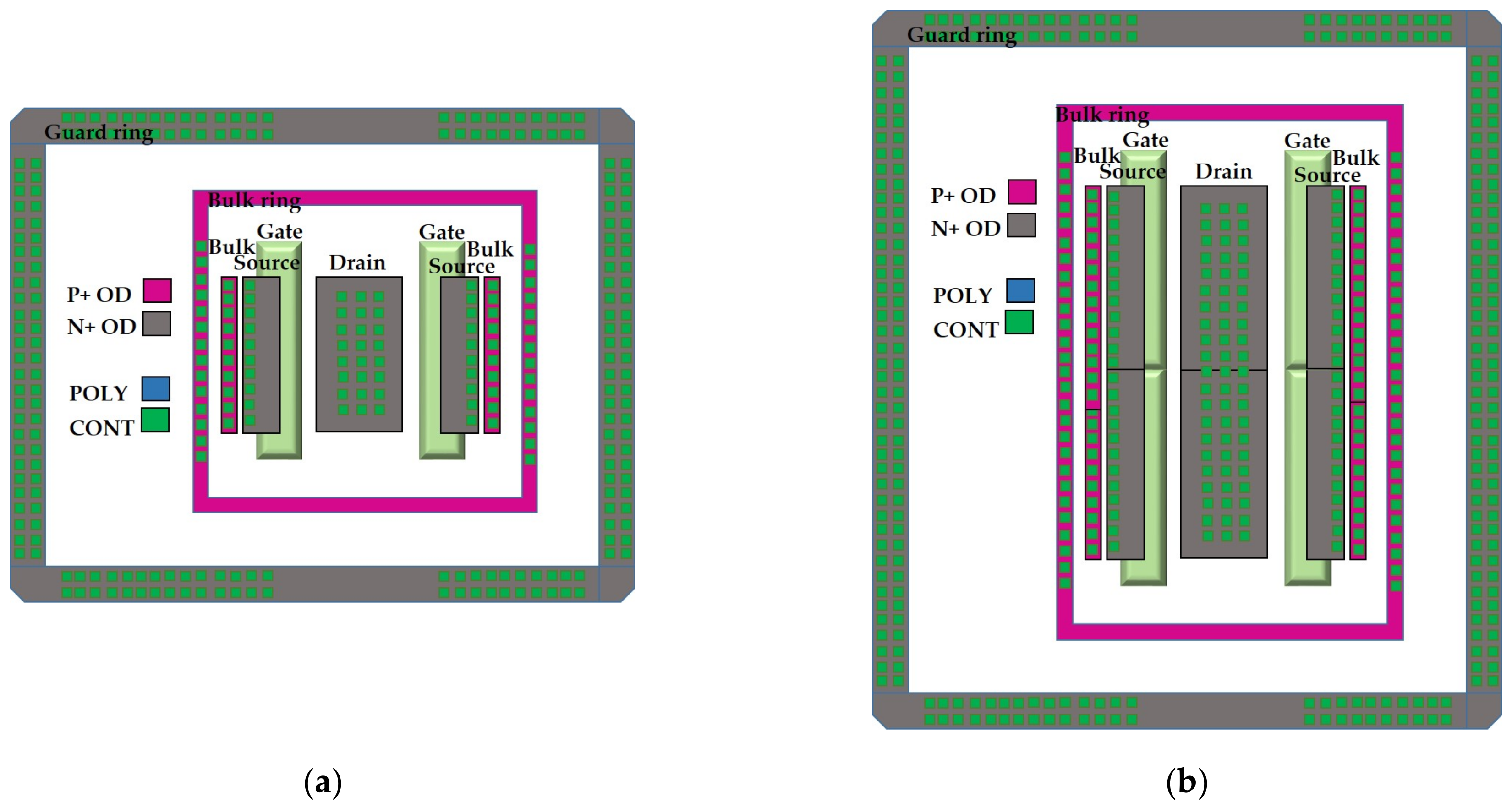
Figure 5.
3D structure views of an HV nLDMOS-SCR with drain-side; (a) NPN-arranged type, (b) PNP-arranged type; (c) NPNPN-arranged type; and (d) PNPNP-arranged type.
Figure 5.
3D structure views of an HV nLDMOS-SCR with drain-side; (a) NPN-arranged type, (b) PNP-arranged type; (c) NPNPN-arranged type; and (d) PNPNP-arranged type.
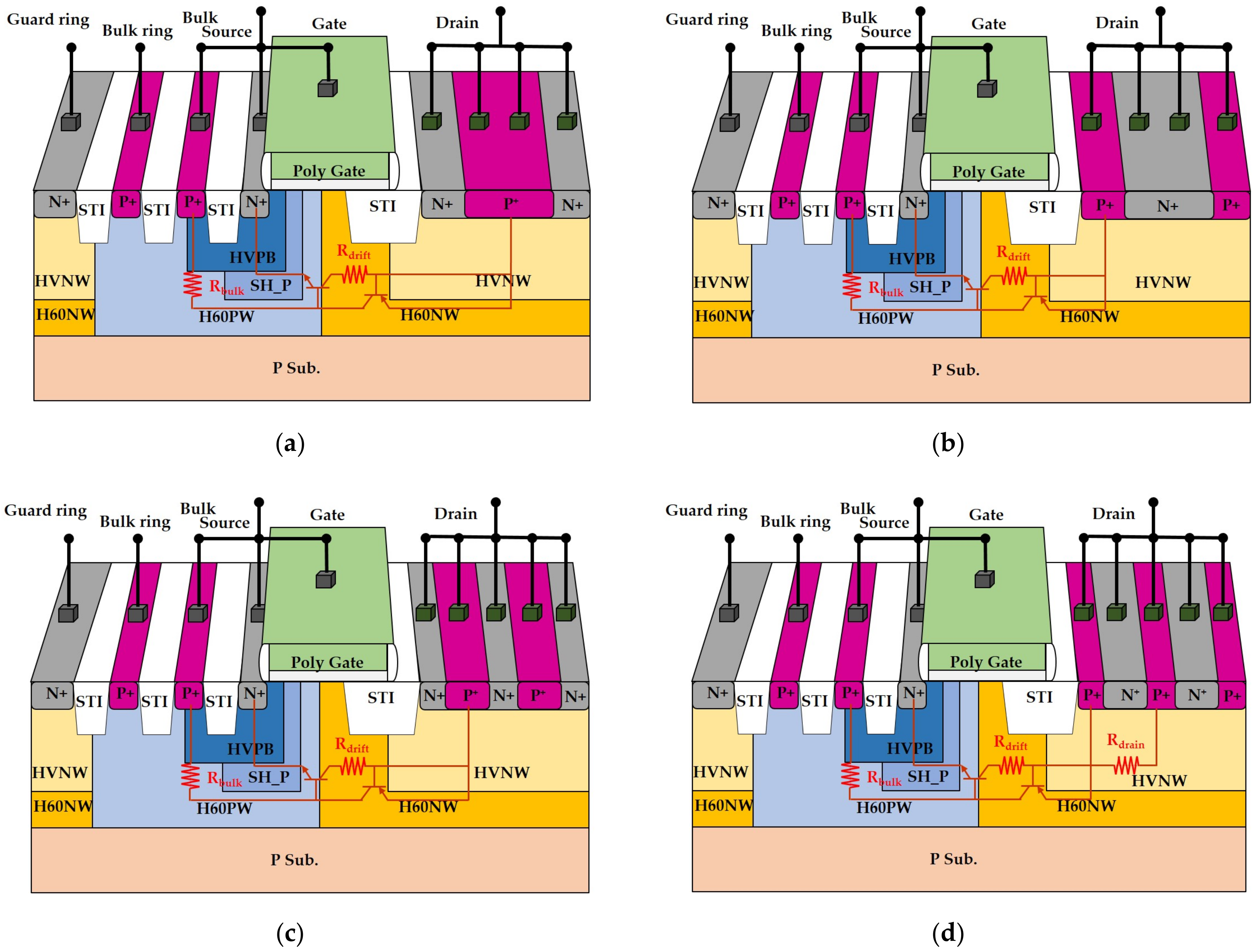
Figure 6.
Parasitic equivalent circuits of an HV nLDMOS-SCR with drain-side; (a) NPN-arranged type; and (b) PNP-arranged type.
Figure 6.
Parasitic equivalent circuits of an HV nLDMOS-SCR with drain-side; (a) NPN-arranged type; and (b) PNP-arranged type.

Figure 7.
3D structure views of HV nLDMOS as with (a) full removing N+ heavy doping, and (b) a central-type embedded Schottky diode modulation in the drain side.
Figure 7.
3D structure views of HV nLDMOS as with (a) full removing N+ heavy doping, and (b) a central-type embedded Schottky diode modulation in the drain side.
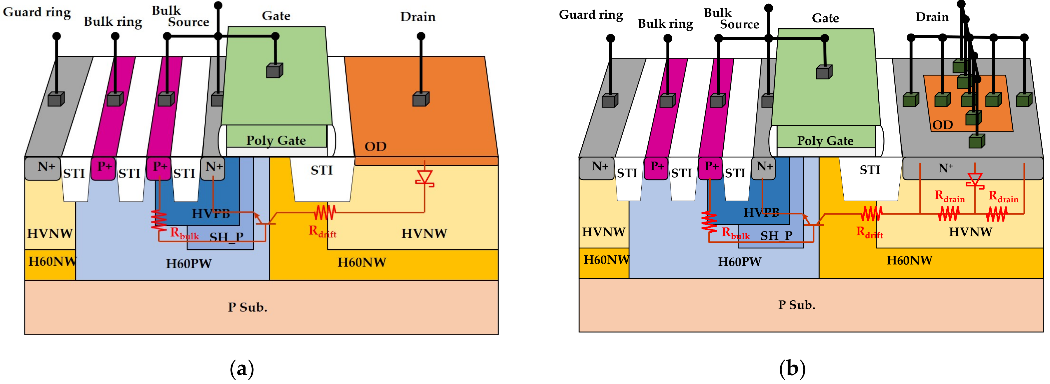
Figure 8.
Parasitic equivalent circuits of an HV nLDMOS with drain-side (a) full removing N+ heavy doping, and (b) a central-type embedded Schottky diode modulation in the drain side.
Figure 8.
Parasitic equivalent circuits of an HV nLDMOS with drain-side (a) full removing N+ heavy doping, and (b) a central-type embedded Schottky diode modulation in the drain side.
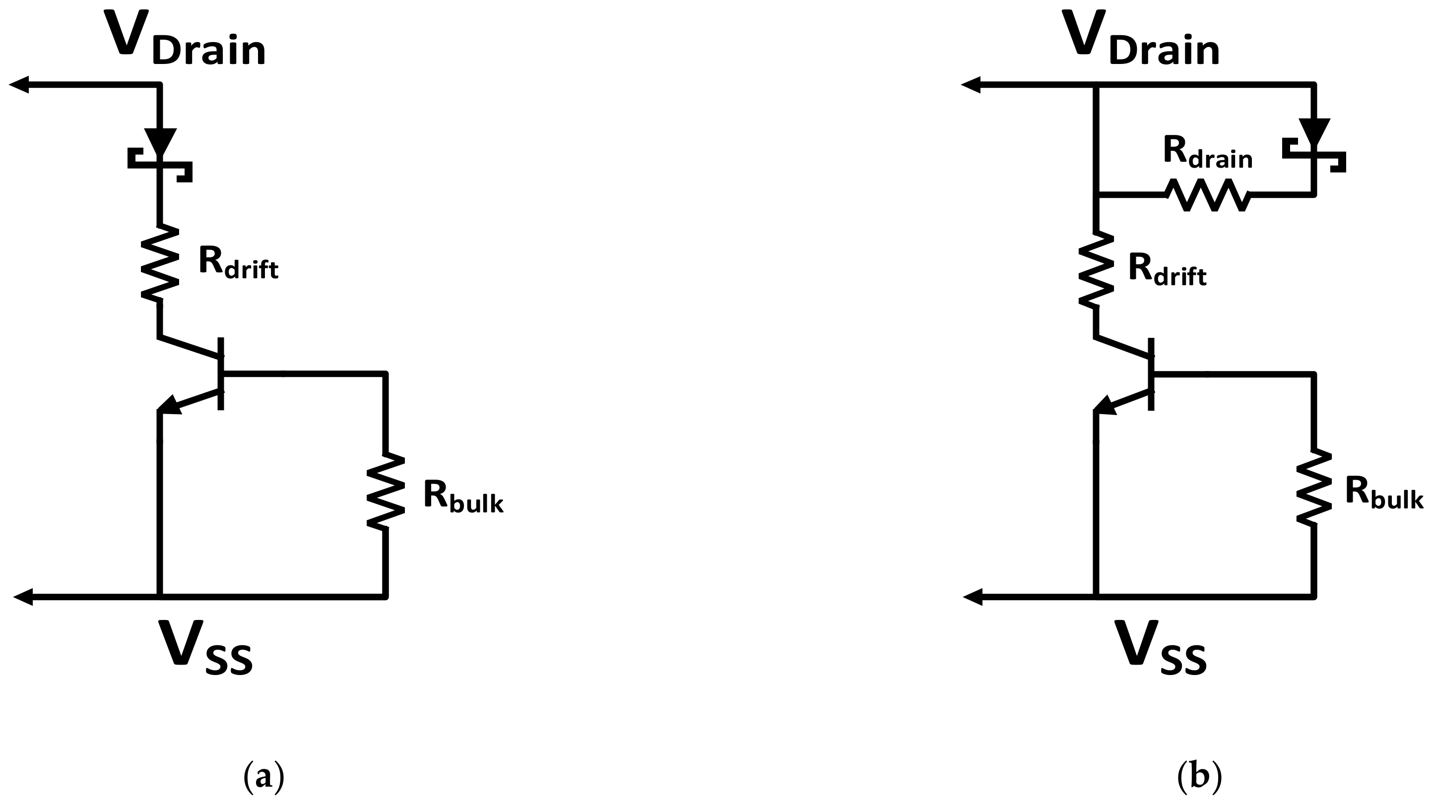
Figure 9.
Snapback I-V curves and leakage currents of HV nLDMOSs with drift-region modulation.
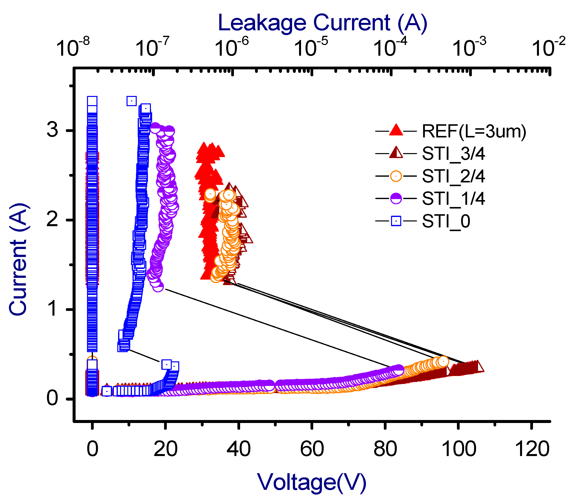
Figure 10.
Trigger voltage/holding voltage distribution charts of HV nLDMOSs with drift-region modulation.
Figure 10.
Trigger voltage/holding voltage distribution charts of HV nLDMOSs with drift-region modulation.
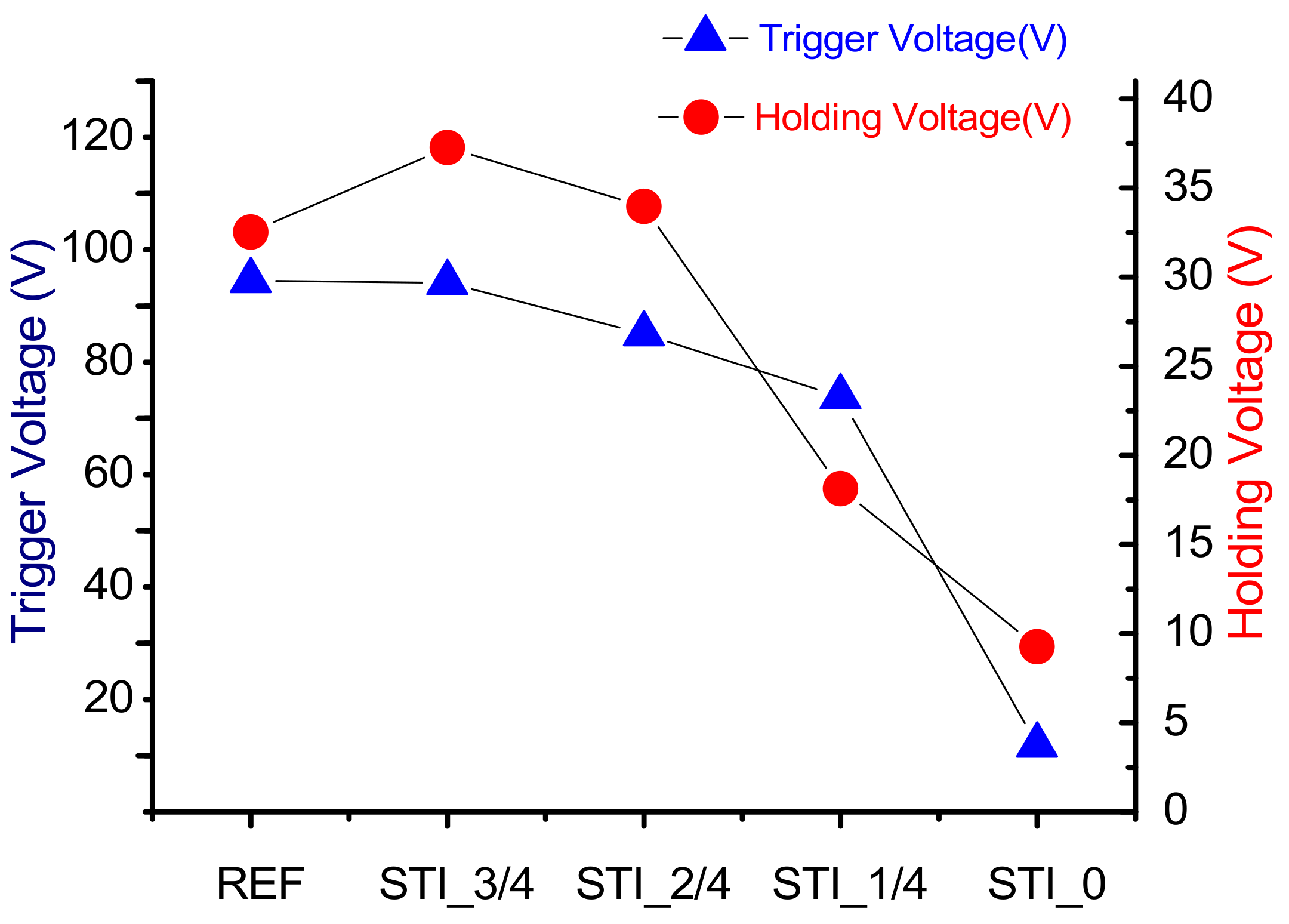
Figure 11.
Secondary breakdown-current distribution chart of HV nLDMOSs with drift-region modulation.
Figure 11.
Secondary breakdown-current distribution chart of HV nLDMOSs with drift-region modulation.
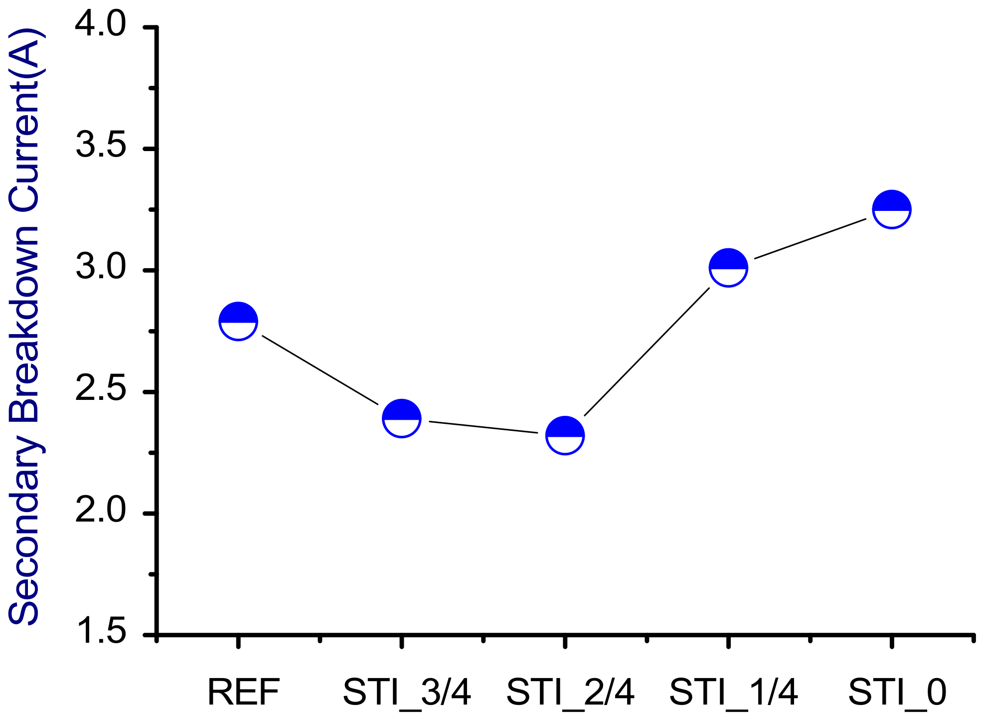
Figure 12.
Snapback I-V curves and leakage currents of HV nLDMOSs with channel-width modulation.

Figure 13.
Trigger voltage/holding voltage distribution charts of HV nLDMOSs with channel-width modulation.
Figure 13.
Trigger voltage/holding voltage distribution charts of HV nLDMOSs with channel-width modulation.

Figure 14.
Secondary breakdown-current distribution chart of HV nLDMOSs with channel-width modulation.
Figure 14.
Secondary breakdown-current distribution chart of HV nLDMOSs with channel-width modulation.

Figure 15.
Snapback I-V curves and leakage currents of HV nLDMOSs with embedded SCR modulation.
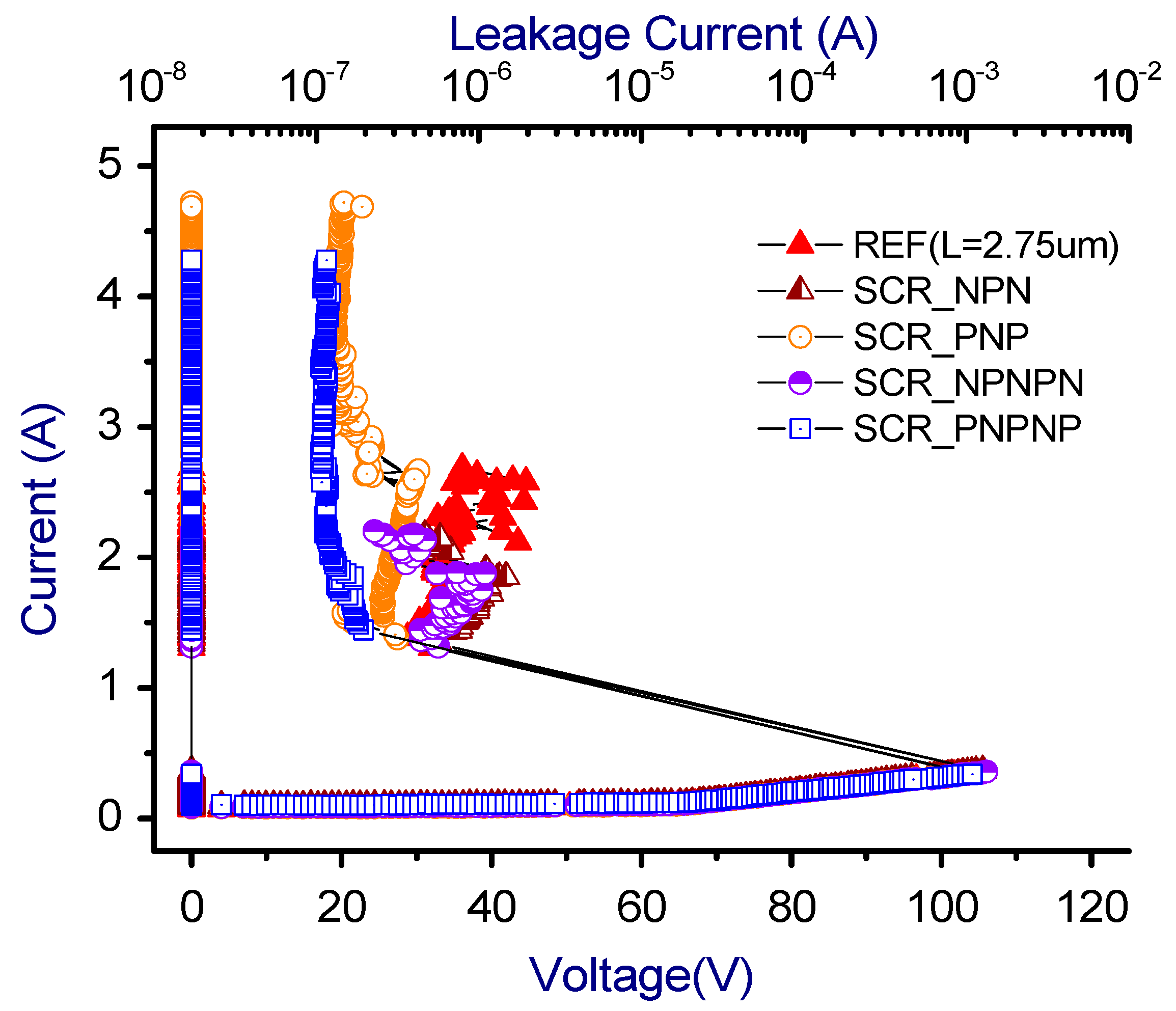
Figure 16.
Trigger voltage/holding voltage distribution charts of HV nLDMOSs with embedded SCR modulation.
Figure 16.
Trigger voltage/holding voltage distribution charts of HV nLDMOSs with embedded SCR modulation.
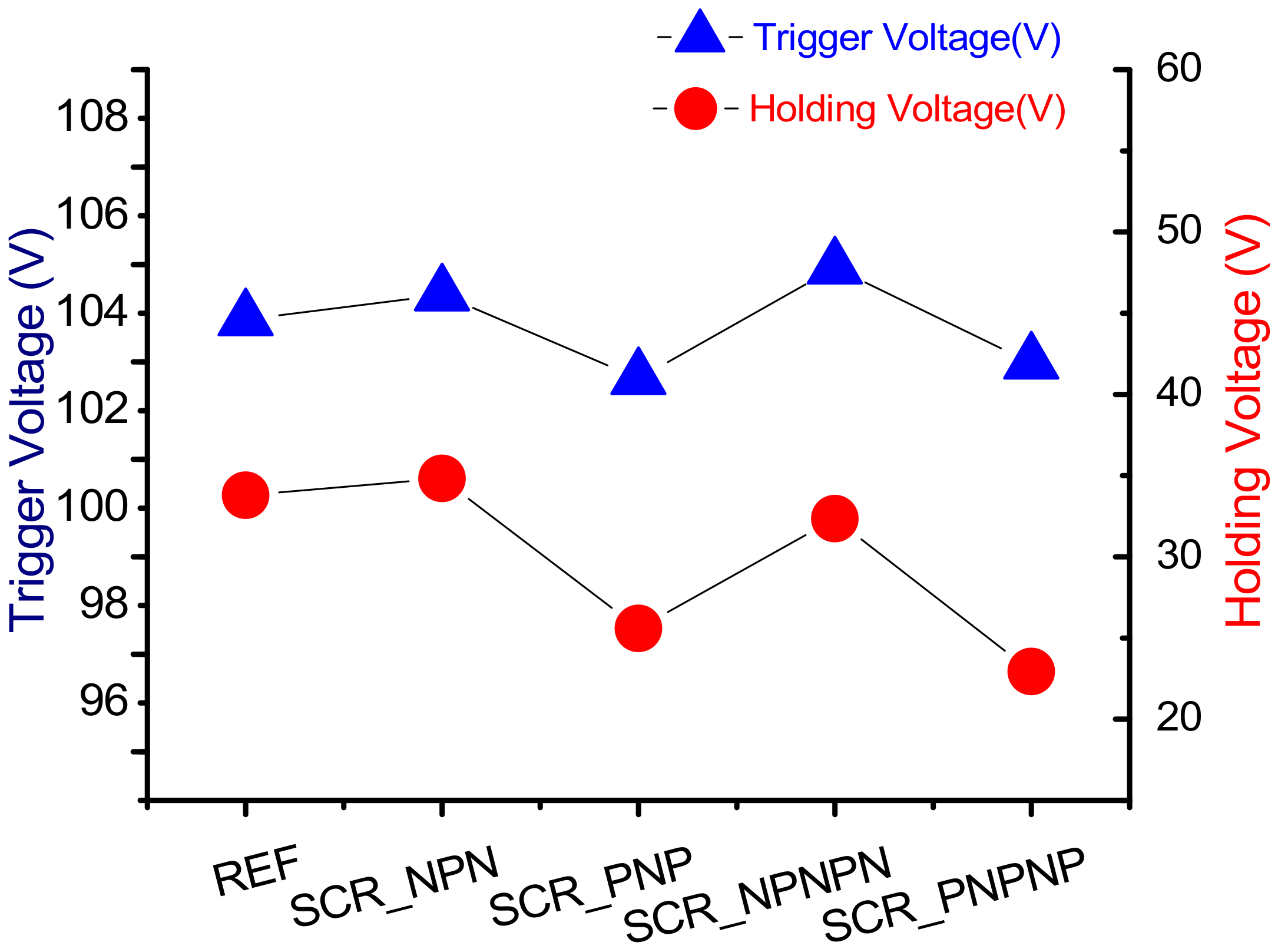
Figure 17.
Secondary breakdown-current distribution chart of HV nLDMOSs with embedded SCR modulation.
Figure 17.
Secondary breakdown-current distribution chart of HV nLDMOSs with embedded SCR modulation.
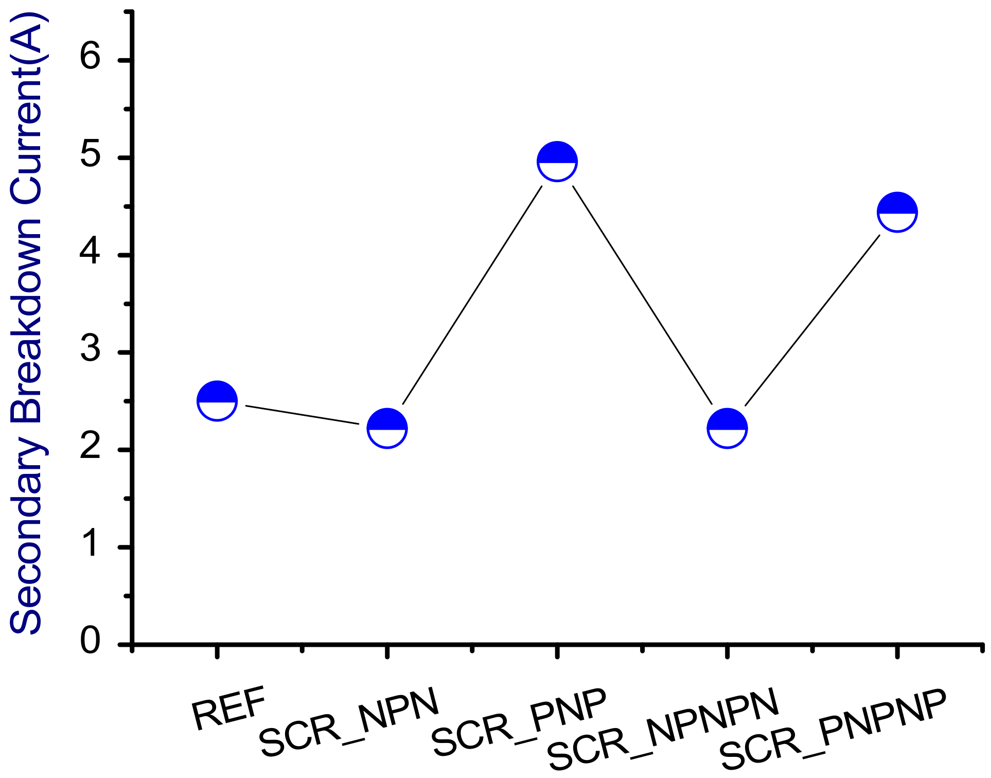
Figure 18.
Snapback I-V curves and leakage currents of HV nLDMOSs with embedded Schottky-diode modulation.
Figure 18.
Snapback I-V curves and leakage currents of HV nLDMOSs with embedded Schottky-diode modulation.
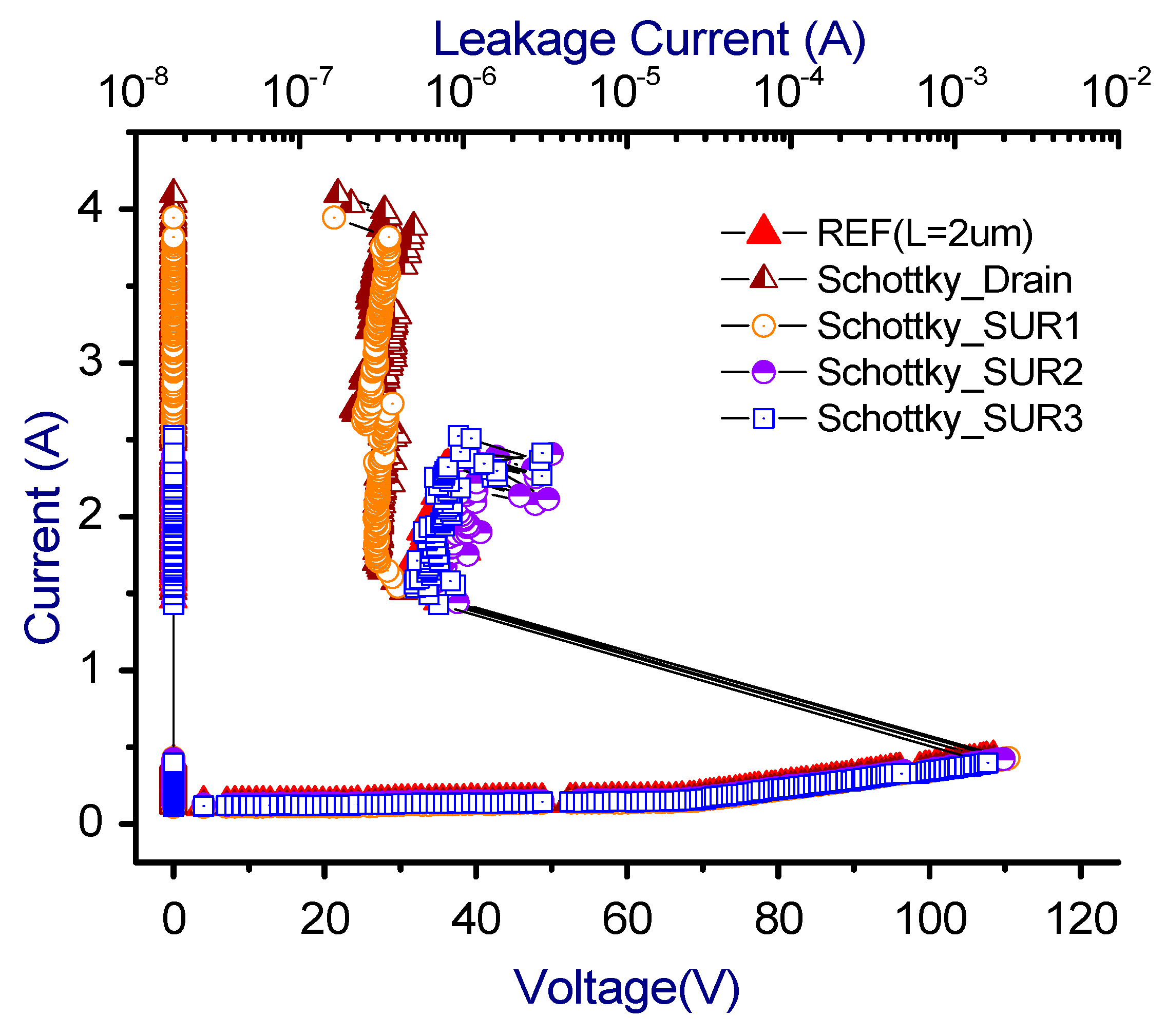
Figure 19.
Trigger voltage/holding voltage distribution charts of HV nLDMOSs with embedded Schottky-diode modulation.
Figure 19.
Trigger voltage/holding voltage distribution charts of HV nLDMOSs with embedded Schottky-diode modulation.

Figure 20.
Secondary breakdown current distribution chart of HV nLDMOSs with embedded Schottky-diode modulation.
Figure 20.
Secondary breakdown current distribution chart of HV nLDMOSs with embedded Schottky-diode modulation.

Figure 21.
Total current-density diagrams of (a) Reference; (b) Schottky_Drain; (c) Schottky_SUR1; (d) Schottky_SUR2; and (e) Schottky_SUR3 at Id = 1 × 10⁻⁴ A injection condition.
Figure 21.
Total current-density diagrams of (a) Reference; (b) Schottky_Drain; (c) Schottky_SUR1; (d) Schottky_SUR2; and (e) Schottky_SUR3 at Id = 1 × 10⁻⁴ A injection condition.

Figure 22.
Lattice temperature diagrams of; (a) Reference; (b) Schottky_Drain; (c) Schottky_SUR1; (d) Schottky_SUR2; and (e) Schottky_SUR3 at Id = 1 × 10⁻⁴ A injection condition.
Figure 22.
Lattice temperature diagrams of; (a) Reference; (b) Schottky_Drain; (c) Schottky_SUR1; (d) Schottky_SUR2; and (e) Schottky_SUR3 at Id = 1 × 10⁻⁴ A injection condition.


Table 1.
Area ratios of N+ and Schottky diode regions in the drain electrode.
| nLDMOS | N+ (%) | Schottky (%) |
|---|---|---|
| Schottky_Drain | 0 | 100 |
| Schottky_SUR1 | 72 | 28 |
| Schottky_SUR2 | 84 | 16 |
| Schottky_SUR3 | 91 | 9 |
| Ref. DUT (L= 2 μm) | 100 | 0 |
Table 2.
Snapback extracted parameters of HV nLDMOSs with drift-region modulation.
| nLDMOS | Vt1 (V) | Vh (V) | Vt1-Vh (V) | It2 (A) | Vbk (V) | FOM (μA × V/μm2) |
|---|---|---|---|---|---|---|
| Ref (L = 3 μm) | 104.47 | 32.53 | 71.94 | 2.79 | 23.52 | 2938.50 |
| STI_3/4 | 104.10 | 37.27 | 66.83 | 2.39 | 23.45 | 3045.68 |
| STI_2/4 | 95.02 | 33.97 | 61.05 | 2.32 | 23.40 | 2948.87 |
| STI_1/4 | 83.82 | 18.13 | 65.69 | 3.01 | 23.10 | 2194.21 |
| STI0 | 21.85 | 9.27 | 12.58 | 3.25 | 11.12 | 1309.59 |
Table 3.
Snapback extracted parameters of HV nLDMOSs with channel-width modulation.
| nLDMOS | Vt1 (V) | Vh (V) | It2 (A) | FOM (μA × V/μm2) |
|---|---|---|---|---|
| Ref. (M4_W300, L = 2.75 μm) | 104.87 | 33.79 | 2.50 | 2836.95 |
| M2_W150 | 102.96 | 36.05 | 2.45 | 4691.93 |
| M2_W300 | 105.99 | 34.66 | 2.73 | 3257.45 |
Table 4.
Snapback extracted parameters of HV nLDMOSs with embedded SCR modulation.
| nLDMOS | Vt1 (V) | Vh (V) | It2 (A) | FOM (μA × V/μm2) |
|---|---|---|---|---|
| REF (L = 2.75 μm) | 104.87 | 33.79 | 2.50 | 2831.83 |
| SCR_NPN | 105.38 | 34.83 | 2.22 | 2587.60 |
| SCR_PNP | 103.66 | 25.59 | 4.96 | 4255.51 |
| SCR_NPNPN | 105.93 | 32.35 | 2.22 | 2406.87 |
| SCR_PNPNP | 103.98 | 22.93 | 4.44 | 3410.64 |
Table 5.
Snapback extracted parameters of HV nLDMOSs with embedded Schottky-diode modulation.
| nLDMOS | Vt1 (V) | Vh (V) | It2 (A) | FOM (μA × V/μm2) |
|---|---|---|---|---|
| Schottky_Drain | 109.43 | 32.54 | 3.98 | 4341.27 |
| Schottky_SUR1 | 109.28 | 29.66 | 3.75 | 3728.36 |
| Schottky_SUR2 | 109.22 | 33.32 | 2.40 | 2680.60 |
| Schottky_SUR3 | 108.51 | 32.88 | 2.34 | 2579.07 |
| Ref. (L = 2 μm) | 107.92 | 31.27 | 2.29 | 2400.38 |
Table 6.
A comparison of FOM improvement percentages for four ESD strengthening methods.
| Samples | FOM (μA × V/μm2) | Improvement |
|---|---|---|
| Method-1: STI_3/4 | 3045.68 | 3.65% ↑ |
| Method-2: M2_W150 | 4691.93 | 65.39% ↑ |
| Method-3: SCR_PNP | 4255.51 | 50.27% ↑ |
| Method-4: Schottky_Drain | 4341.27 | 80.86% ↑ |
© 2020 by the authors. Licensee MDPI, Basel, Switzerland. This article is an open access article distributed under the terms and conditions of the Creative Commons Attribution (CC BY) license (http://creativecommons.org/licenses/by/4.0/).
Share and Cite
MDPI and ACS Style
Fan, S.-K.; Chen, S.-L.; Lin, P.-L.; Chen, H.-W. Layout Strengthening the ESD Performance for High-Voltage N-Channel Lateral Diffused MOSFETs. Electronics 2020, 9, 718. https://doi.org/10.3390/electronics9050718
AMA Style
Fan S-K, Chen S-L, Lin P-L, Chen H-W. Layout Strengthening the ESD Performance for High-Voltage N-Channel Lateral Diffused MOSFETs. Electronics. 2020; 9(5):718. https://doi.org/10.3390/electronics9050718
Chicago/Turabian StyleFan, Sheng-Kai, Shen-Li Chen, Po-Lin Lin, and Hung-Wei Chen. 2020. "Layout Strengthening the ESD Performance for High-Voltage N-Channel Lateral Diffused MOSFETs" Electronics 9, no. 5: 718. https://doi.org/10.3390/electronics9050718
Note that from the first issue of 2016, this journal uses article numbers instead of page numbers. See further details here.