Article

Multi-Mode Interferometry: Application to TiO2–SiO2 Sol-Gel Waveguide-Based Sensing in the Aerospace Domain

1
Laboratoire H. Curien, UJM-CNRS-IOGS, Université de Saint-Etienne, 18 Rue Du Pr. Benoît Lauras, 42000 Saint-Etienne, France
2
Photonfirst, Pyrietstraat 2, 1812 SC Alkmaar, The Netherlands
3
Formerly at Airbus, 316 route de Bayonne, 31060 Toulouse, France
4
Airbus Operations Ltd., Filton, Bristol BS34 7PA, UK
*
Author to whom correspondence should be addressed.
These authors contributed equally to this work.
Aerospace 2021, 8(12), 401; https://doi.org/10.3390/aerospace8120401
Submission received: 12 November 2021 / Revised: 14 December 2021 / Accepted: 15 December 2021 / Published: 18 December 2021

Abstract

:
The optimization of a 2D optical sensor based on TiO2–SiO2 sol-gel waveguides for damage detection in the aerospace domain was performed in the framework of the ADD-ON European project. The sensor is based on the transportation of visible light along numerous waveguides, and damage is detected and localized through the monitoring of the output light from the waveguide grid. In this work, we have developed an architecture, inspired by a multi-mode interferometer (MMI), allowing us to efficiently multiply the number of waveguides that can be probed by a single optical source. For this, the beam propagation method (BPM) was used to model a rectangular MMI coupler (40 × 5624 µm2) operating in the visible region (600 nm), ensuring the propagation of light into three waveguides. The conceived device was then manufactured by UV photolithography (direct laser writing technique). The simulations and experimental results show that light transport into this architecture allows for the successful simultaneous probing of three waveguides. By complexifying the device structure, successful MMI couplers were easily manufactured, allowing us to probe 9, 15, or 45 TiO2–SiO2 waveguides with a unique light source. Finally, a further investigation regarding 24 consecutive thermal cycles from −40 °C to 60 °C, representative of the temperature changes during aircraft cruising, was performed. This study reveals that TiO2–SiO2 sol-gel waveguides are not mechanically damaged by temperature changes, while the light guidance remains unaffected, confirming that this sensor is very promising for aerospace applications. Since a single source can monitor several guides, the production of more compact, low-cost, and less intrusive sensors can be achieved by fulfilling structural health monitoring requirements.

1. Introduction

Structural health monitoring (SHM) is a crucial and popular process involving the analysis and observation of infrastructures in order to identify anomalies originating from deterioration or damage [1]. This powerful tool can concern the monitoring of buildings [2], bridges [3], or even architectures operating in the aerospace domain [4], namely in the civil aviation industry. For this latter, several techniques have been deployed over the years in order to check deterioration at early stages, before significant degradation can occur. Among all these techniques, we can mention the use of piezoelectric wafer active sensors [5] or acousto-ultrasonic monitoring systems [6]. In addition to these principles, optical fiber sensors (OFSs), based on light transport, can also be of interest regarding the in-situ monitoring of aircraft architectures. Basically, applications using OFSs are largely detailed in the literature where fiber-optic interferometers [7,8] allow temperature, strain, or refractive index (n) evaluations, while Bragg grating-based [9] and Brillouin or Rayleigh-based sensors operate as quasi-distributed and distributed measurements. Alternative ways, related to guided optics, can be used regarding SHM applications. For example, we have recently evidenced the potential of a low-weight, low-cost, and non-intrusive sol-gel sensor, operating in the aerospace domain, to detect and localize damage on large surfaces [10]. This latter is investigated in the framework of the Clean Sky 2 (Horizon 2020) ADD-ON project (Advanced Damage Detection through Optical Sensor Network). The sol-gel process is a soft chemical route allowing for the development of glass-like materials [11] where metal alkoxide precursors are used to form an inorganic metal oxides matrix. Coupling this particular process with UV (ultra-violet) photolithographic techniques allows for the micro-structuration and patterning of sol-gel-based materials. More specifically, the ability to pattern such materials relies on their photosensitivity with respect to UV photons: sol-gel films are listed as negative photoresists, implying that the UV-exposed area is polymerized and densified. After a development procedure, in an alcoholic solution (ethanol, butanol, propanol, etc.), the zones exposed to photons are resistant to alcohol while the unexposed zones are dissolved, allowing us to reveal sol-gel components for which applications can be achieved in many fields [12,13,14]. The SHM device, already largely introduced in [10], was manufactured using the direct laser writing technique and is schematically illustrated in Figure 1a. It consists of TiO2–SiO2 sol-gel waveguides on large surfaces (30 cm × 35 cm) arranged in a 2D matrix and based on light transport while a ZrO2–SiO2 cladding acts as a buffer layer. After the injection of light in all the TiO2–SiO2 structures through optical fibers, we showed that the localization of damage is deduced from the optical mode extinction due to the rupture of one or more TiO2–SiO2 guides. For example, Figure 1b shows an overview of a 2D waveguide grid on large surfaces deposited on soda-lime glass, while a zoomed-in image is given in Figure 1c.
However, even if this robust technique shows satisfying results, the actual configuration implies that one source (typically one optical fiber) monitors a single straight waveguide. In order to obtain access to miniaturized components leading to higher flexibility and lower costs, this paper is dedicated to the development of more complex TiO2–SiO2 sol-gel photonic devices within the ADD-ON project. These structures are based on MMI (multi-mode interferometers) couplers inspired by the literature [15,16] and which act as splitters, where accurate splitting ratios between guides can be obtained. Thus, this paper aims at giving additional information and is related to the optimization of the 2D waveguide grid. We present results regarding the creation of MMI couplers, confronting simulation and an experimental point of view, revealing the feasibility of multiplying the number of TiO2–SiO2 guides probed with a unique optical source, leading to the creation of more compact components, while the coupling efficiency from optical fiber to sol-gel waveguides is simulated in different configurations. The mechanical resistance of these waveguides was also evaluated in our previous article [10], from 80 °C down to −40 °C, showing that the integrity of those waveguides was not affected by temperature changes between the takeoff and landing for a single thermal cycle. To complete these preliminary results, further experiments have been performed during 24 complete thermal cycles by also monitoring the output light of the waveguides. The presented results confirm the high potential of such photonic devices in the aerospace domain for SHM applications.

2. Materials and Methods

2.1. Sol-Gel Elaboration

Both waveguides and MMI couplers were created using a specific homemade organo-titania-silica (TiO2–SiO2) sol-gel, the elaboration of which has already been published and detailed in our previous papers [10,17]. However, this latter is briefly recalled hereafter. The hybrid sol-gel results from the mixture of 3–(trimethoxysilyl)propyl methacrylate (TMSPMA, silicate precursor), titanium (IV) isopropoxide (TIPT, titanium precursor), and 2–(methacryloyloxy)ethyl acetoacetate (AAEM) acting as the chelating agent. All these precursors were provided by Sigma-Aldrich (Saint-Quentin Fallavier, France). In summary, two solutions were prepared. The first one was elaborated by the addition of AAEM in TIPT while the second one consists of the incorporation of HCl in TMSPMA. Both solutions were mixed and water was added to induce hydrolysis. Finally, a photo-initiator (2,2-dimethoxy-2-phenylacetophenone) was incorporated to enhance UV photopolymerization (already induced by precursor organic chains) in the form of 0.7 wt.%. The resulting molar ratio of precursors Si:Ti:AAEM was fixed at 10:10:5.5.

2.2. Creation of TiO2–SiO2 Photonic Devices

Thin films of TiO2–SiO2 were deposited in a clean room at a fixed temperature (20 °C) and hygrometry (50%) by the spin coating approach at 4000 rotations per minute (RPM) on soda-lime glass inducing a film thickness between 4 and 5 µm. Once deposited, a preliminary heat treatment was performed at 60 °C for 5 min, thus ensuring the evaporation of the solvents. This step was followed by the photolithographic process. UV exposure, in order to create TiO2–SiO2 photo-induced devices, was performed using the Dilase 750 facility (Kloé, Montpellier, France), a photolithography machine based on the direct laser writing technique whose description is detailed in [10]. More specifically, a continuous-wave laser, providing UV light at 375 nm with 26 mW of power, was focused on the sol-gel layers through a × 10 microscope objective with a nominal Numerical Aperture (NA) of 0.3. In this particular condition, the creation of sol-gel patterns is determined by the translation of a computer-controlled stage while the focused laser beam remains fixed. This configuration allows access to a resolution and repeatability of 100 nm. Controlling both laser power and scanning speed determines the lateral dimensions of the devices being manufactured. Additionally, a NE10A optical density (OD) can also be placed on the optical path to adjust the power (Thorlabs, Newton, NJ, USA). This condition is necessary to create architectures with the highest resolution. For example, at 375 nm, a light transmission of 1.9% is achieved, resulting in an OD of 1.72. After the photolithography process, the layers were placed in a butanol solution: the non-exposed parts corresponding to the unpolymerized regions were removed, thus revealing the sol-gel devices insofar as sol-gels act as negative photoresists. Films were finally post-baked at 90 °C for 30 min to harden the layers. Before probing the sol-gel waveguides or MMI couplers, both sides of the sample were cleaved so that a proper light injection and collection could be achieved.

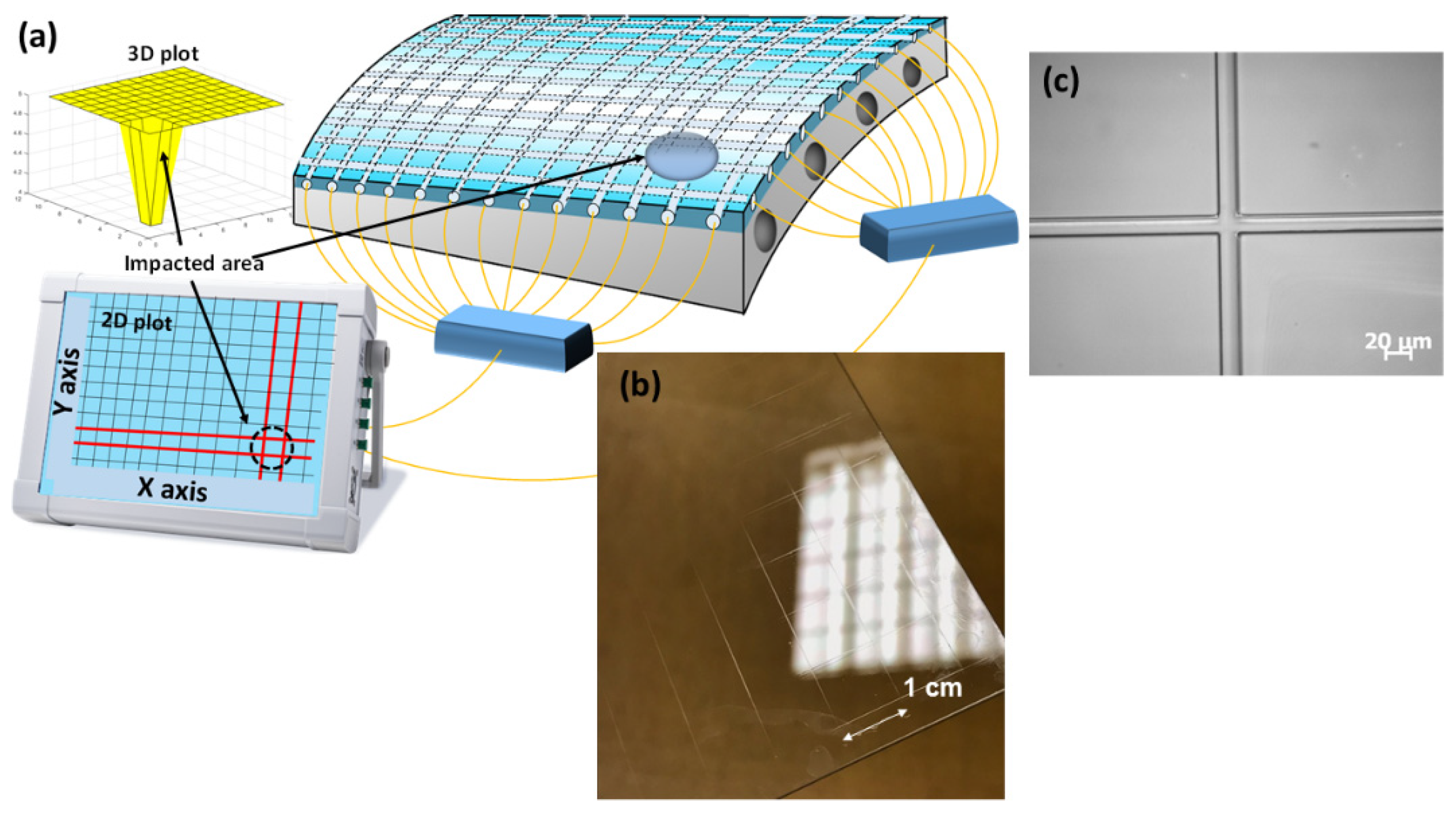
2.3. Characterization of TiO2–SiO2 Devices

The photo-induced devices were characterized using an Axio imager M1m optical microscope (Zeiss, Marly le Roi, France) operating in reflection mode while a Dektak profilometer (Bruker, Palaiseau, France) was employed to quantify the shapes, widths, and thicknesses by probing samples with a stylus force of 15 mg. Two different light sources were used in order to study the optical properties (light guidance) of the inscribed waveguides: a fibered laser diode operating at 638 nm (Thorlabs, Newton, NJ, USA) and a homemade supercontinuum white light source ranging from 350 nm to 2000 nm. The setup, dedicated to light propagation, is depicted in Figure 2 and is composed of a single-mode optical fiber (SMF28 from Corning, Corning, NY, USA) with a core diameter of 8 µm. This latter was placed on a V-groove, thus ensuring high stability where motion can be achieved in the XYZ directions. The light injection inside the different sol-gel devices was performed through a butt-coupling configuration. A first camera, coupled with an objective (not shown), allows for a top-view image (XZ-plane) in order to optimize the light injection inside the waveguides, while another camera, whose translation can be performed along the Z-axis, is dedicated to the output light observation once imaged through a long working distance 20 × microscope objective (NA = 0.42).

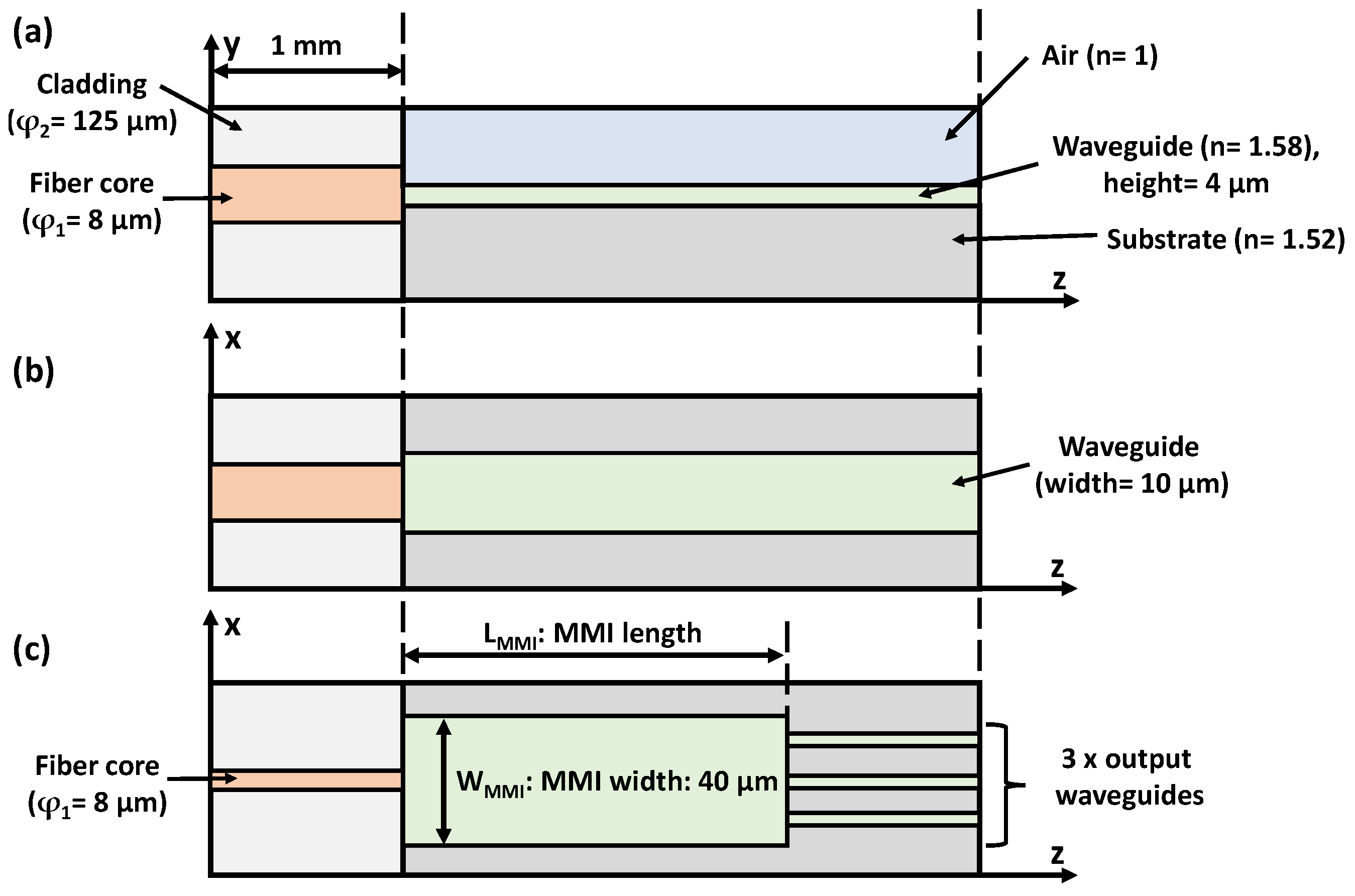
2.4. Simulation Tools: Waveguides and MMI Couplers

All the simulations presented at 600 nm in this manuscript were obtained based on the beam propagation method (BPM) and related to the behavior of light through a waveguiding medium. The SMF28 was modeled as a cylinder of 1 mm length while a diameter core (φ1) and cladding (φ2) of 8 µm and 125 µm, respectively, were fixed. The corresponding refractive index contrast between the core and the cladding was 5 × 10⁻³ and a butt-coupling injection was simulated between the single-mode fiber and the TiO2–SiO2 sol-gel waveguide (n = 1.58 at 600 nm). This latter is designed as a rectangle whose width and thickness are 10 µm and 4 µm, respectively. All simulations were performed assuming that the waveguides were placed on soda-lime glass (n = 1.52) and surrounded by air (n = 1) as shown in Figure 3, where the YZ- (a) and XZ-planes (b) are given.
In addition to the simulation of straight waveguides, we have modeled N × M MMI couplers using the same sol-gel material where N and M are related to the numbers of input and output, respectively. Basically, these structures can be mainly seen as large rectangular waveguides supporting a high number of guided modes [18]: their interferences allow for the reconstruction of the input field profile at periodic intervals along the MMI propagation axis (Z), where the superposition of the electromagnetic fields manifests itself as one or several peaks (called images) in the lateral dimension (X-axis). These optical multi-mode interference devices are known to be based on the self-imaging principle largely investigated in the literature [15,18,19,20]. The fact that several images of the input field profile can be reconstructed is of great interest since splitting into several output waveguides is possible, as will be observed in Section 3.3. The MMI length (LMMI) is one of the most crucial and important parameters to be modeled and this quantity can be approximately defined as [16]:
L MMI = n e W e 2 N λ 0
where ne represents the transverse effective index of the waveguide mode, We is the effective MMI width, while λ0 and N are the wavelength and the number of output waveguides, respectively.
Figure 3c shows an example of a 1 × 3 MMI coupler with a 40 µm width (WMMI), ensuring a strongly multi-mode device. An electromagnetic wave at 600 nm is injected via an SMF28 through a butt-coupling approach, while the simulation of the field propagation along the Z-axis is performed, in order to evidence the reconstruction of several images at periodic intervals. WMMI (40 µm) and the thickness (4 µm) being fixed, the simulation allows access to the optimal TiO2–SiO2 MMI length (LMMI), where the field amplitude is uniformly divided by 3, linked to the location of the output waveguides, and to the center-to-center spacing between two consecutive waveguides.

3. Results and Discussion

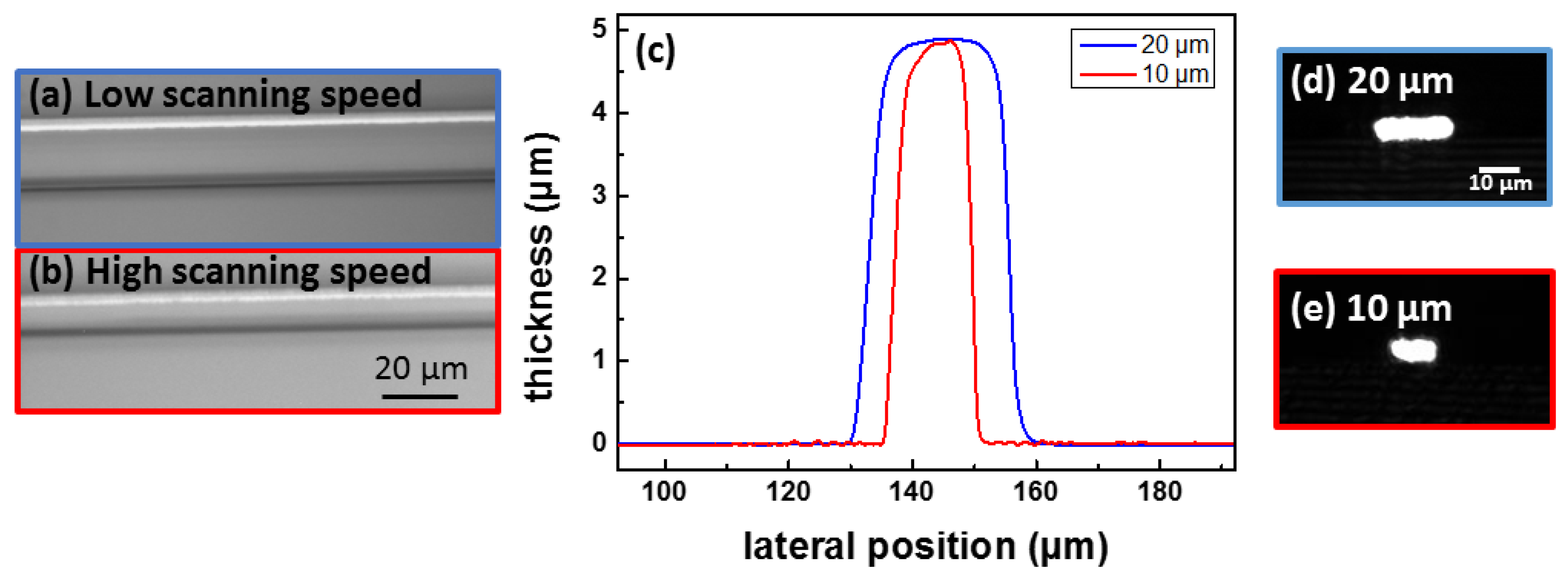
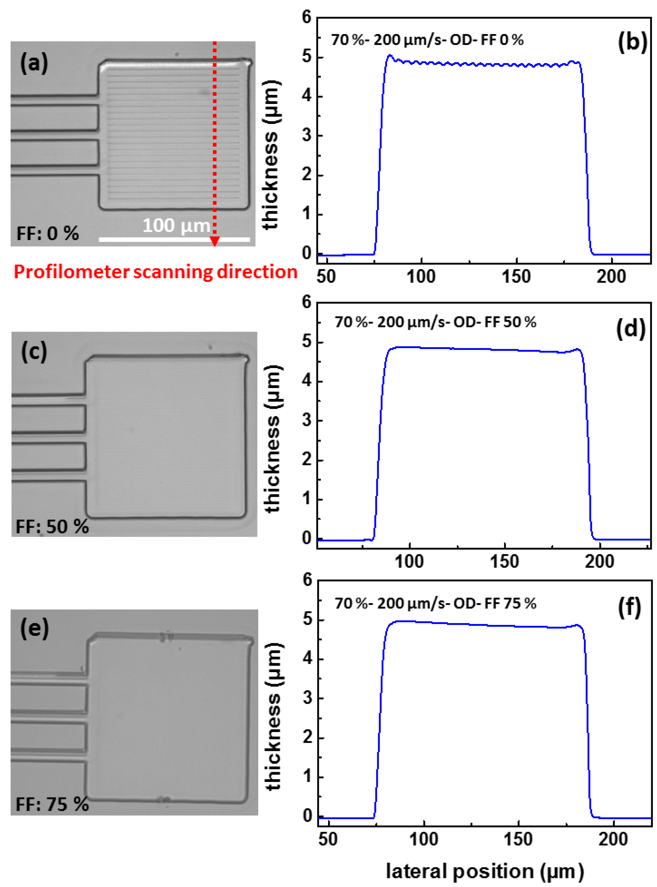
3.1. Creation of TiO2–SiO2 Waveguides by Direct Laser Writing Technique

This part briefly recalls how TiO2–SiO2 sol-gel waveguides are created while their optical properties (namely the refractive index, n) are given. All the structures (straight waveguides or MMI couplers) are photoinduced through the direct laser writing method on a soda-lime glass substrate (n = 1.52 at 600 nm) and surrounded by air (n = 1). The spin coating is fixed in terms of angular speed, the thickness of the structures is in the 4 µm–5 µm range. However, depending on the laser power and the scanning speed, it is possible to tune their widths up to 20–30 µm [10]. For instance, at a fixed laser power, waveguides with high lateral dimensions are obtained, typically 20 µm (Figure 4a) using low scanning speeds while thinner ones (10 µm) can be induced by increasing the stage velocity (Figure 4b). Additionally, their respective shapes, obtained by profilometer measurements, are given in Figure 4c, and their output light distribution was recorded after excitation at 638 nm, as shown in Figure 4d,e. The fact that intense output optical light distribution is observed, whatever their dimensions, is related to two points: TiO2–SiO2 layers are known to be transparent from the visible to the infra-red range [21,22] while their refractive indices, evaluated by ellipsometry, are higher than those of the substrate [10]. For instance, a refractive index of 1.58 can be achieved at 600 nm, leading to a strong refractive index contrast of 6 × 10⁻² between the sol-gel waveguide and the substrate. The estimation of this particular optical constant is of great importance for the development of simulation and predictive tools regarding light guidance, as will be observed in the following parts.

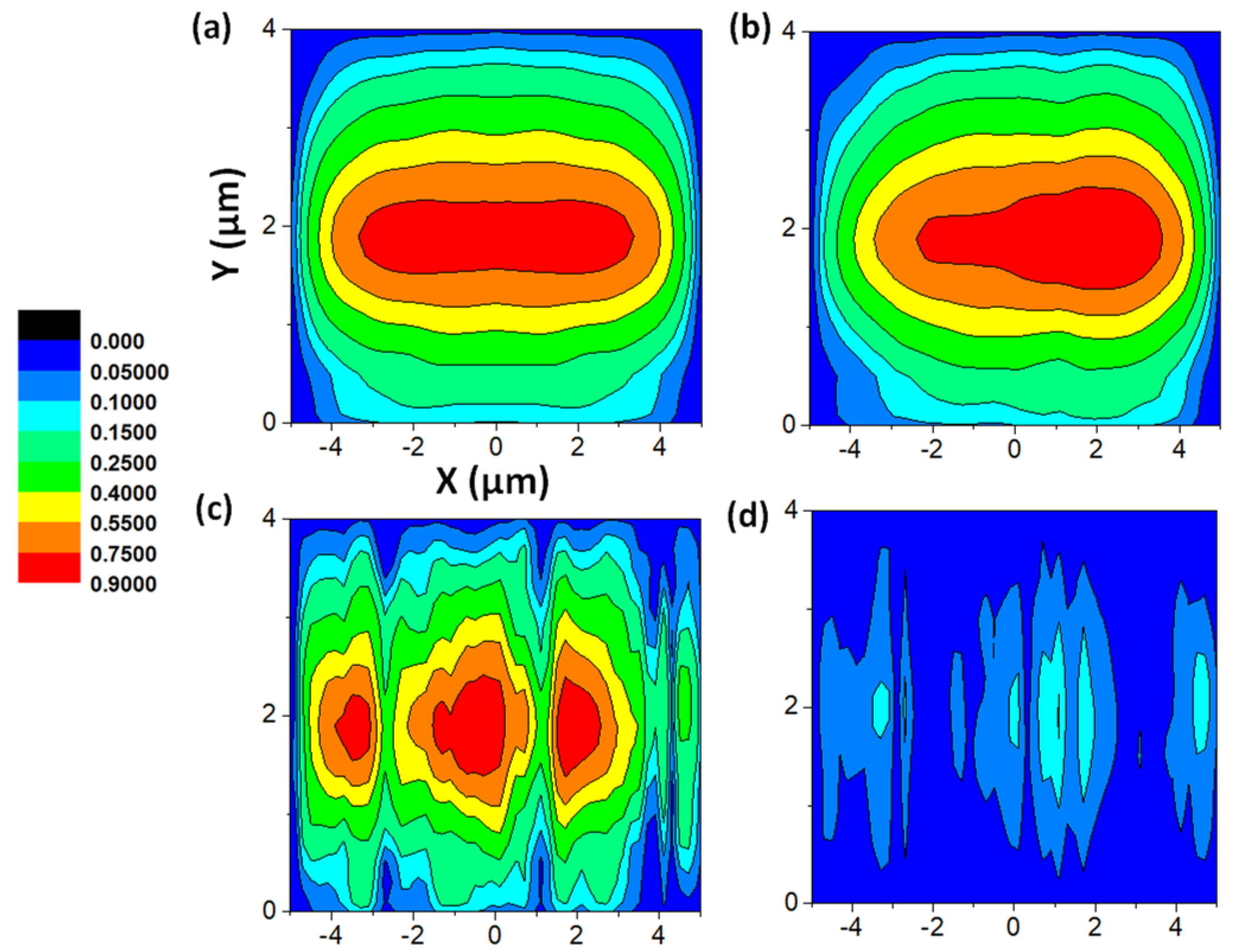
3.2. Optical Fiber and Sol-Gel Waveguide Coupling: Simulation of Connection Losses

Apart from the waveguiding properties, the quality of the light propagation is also related to the connection between the optical fiber (SMF28) and the TiO2–SiO2 waveguides to be probed. Since these two structures have different geometries and shapes, connection losses are induced even with a proper butt-coupling configuration, while an important misalignment can drastically affect the light injection and the reliability of our damage sensor. To this aim, we have estimated the connection losses (at 600 nm) using a simulation-based approach in a perfect injection condition (no misalignment) and for several fiber misalignments along the X-axis of 1 µm, 4 µm, and 8 µm, as shown in Table 1, while the waveguide position is constant. We recall that the parameters (refractive index, geometries) used for the present simulation are depicted in Section 2.4. The sol-gel waveguide thickness is fixed at 4 µm, while two widths are investigated: 10 µm and 30 µm, easily achieved by a direct laser writing technique. In addition to Table 1, we present in Figure 5 the repartition of the optical light power for 10 µm × 4 µm waveguides with different X-axis misalignments: 0 µm (a), 1 µm (b), 4 µm (c), and 8 µm (d).
Since the waveguides and the SMF28 have different shapes and dimensions, connection losses are created. Even with an ideal injection (misalignment: 0 µm), a minimum loss of 15% is induced. For this latter, the light intensity distribution is given in Figure 5a, showing a quasi-symmetric pattern with an intense light collection, while a 1 µm shift (b) will not affect the connection losses. Even if the corresponding intensity distribution seems to be similar compared with the previous simulation (ideal case), the resulting pattern is slightly asymmetric. Higher shifts along the X-axis will lead to an important degradation of both connection losses and distribution shapes. For instance, a 4 µm shift favors connection losses of 35% (Table 1), and the light distribution presents three maximum peaks (c) with a global decrease in the intensity, while an 8 µm shift induces a dramatic decrease in the intensity (d) related to high connection losses (95%). Interestingly, with a higher width (30 µm), the connection losses remain similar (15%) compared with a 10 µm width waveguide. The simulations presented in this section were performed at a fixed thickness (4 µm), while similar results were obtained for thicknesses from 3.5 µm to 5 µm. This range is representative of the range accessible using the spin coating approach (4–5 µm).

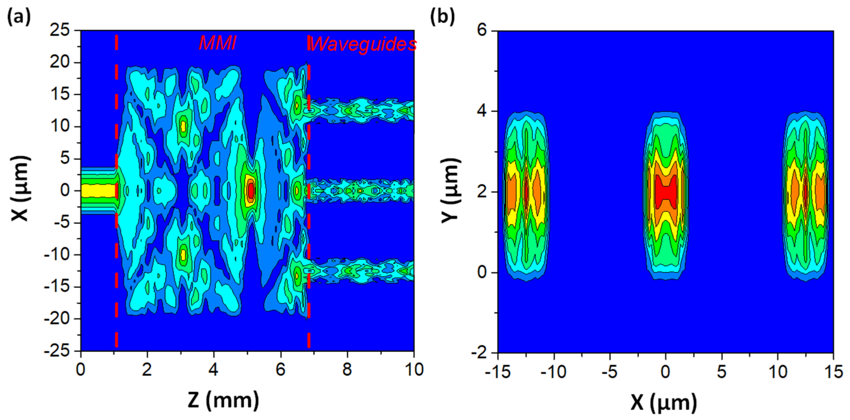
3.3. 1 × 3 MMI Coupler Simulation

As mentioned in Section 2.4, the BPM is used in order to compute the light field propagation into the MMI architecture at a 600 nm wavelength. This is to remind us that WMMI is fixed (40 µm), and the simulation aims at providing the optimal MMI length where three output waveguides start. First, the behavior of self-imaging (Figure 6) in the sol-gel device is obtained for a 40 µm width waveguide after light injection with an SMF28 (left). For all the simulations presented in this section, the fiber is centered (no misalignment) with the waveguide or MMI coupler. The field propagation through the multi-mode waveguide shows several interesting features. The input field is reproduced at periodic intervals along the Z-axis, resulting in single principal images at 4.126 mm and 8.287 mm from the waveguide input. Additionally, we can observe three images (peaks) of interest at four positions along the Z-axis: 1.400 mm, 2.733 mm, 5.624 mm, and 6.860 mm, separated by a 12.5 µm distance in the lateral dimension (X-axis). Obviously, their respective powers are lower compared with a single image since the power is shared. These results clearly indicate the potential MMI length for probing three distinct waveguides.
Considering the position of the three peaks along the Z and X axes, it is possible to design the final MMI coupler to be manufactured using the direct laser writing technique. Among all the four possibilities given by the BPM (1.400 mm, 2.733 mm, 5.624 mm, and 6.860 mm), a 1 × 3 MMI coupler simulation is performed with an LMMI of 5.624 mm, as represented in Figure 7a. The three output waveguides, whose widths are fixed at 5 µm, are placed in accordance with the results obtained in Figure 6 since a center-to-center spacing of 12.5 µm is realized (X-axis). Under this exact configuration, the simulation reveals that light propagation is possible within three different waveguides, using a 40 µm × 5624 µm MMI coupler. Additionally, the three waveguide output spots (600 nm) are given in Figure 7b, showing intense symmetric light patterns where the energy seems to be equally shared between each output spot.

3.4. TiO2–SiO2 MMI Couplers Manufacturing

The creation of MMI couplers is of great importance regarding the manufacturing of photonic sensors: a single source can be used to interrogate several waveguides, leading to the production of more compact sensors. Indeed, the miniaturization of the photonic devices, related to non-intrusive methods, remains a very crucial parameter, especially in the aerospace domain. To this aim, we have focused our work on the feasibility of building more complex architectures such as MMI couplers using the direct writing technique. It should be noted that the MMI-like structures presented in this subsection do not fit with the simulation parameters but aim to provide important information regarding the manufacturing of complex structures using the direct writing approach, namely in terms of surface quality. All the MMI-like structures shown in Figure 8 (microscope image in reflection mode, ×40) are written using 70% of the total laser power, while an OD is placed along the path with a scanning speed of 200 µm/s. Under this condition, a TiO2–SiO2 line waveguide is induced with a lateral dimension of roughly 5–6 µm. The resulting pattern consists of a 100 × 100 µm2 square with three different waveguides separated by a 25 µm distance. In order to fill the square pattern, it is essential to control the filling factor (FF), a crucial parameter determining the surface quality and fostering the best performance possible. Typically, the filling of the square pattern can be achieved by several consecutive polymerized guides where the distance between them (pitch) can be adjusted. The FF allows for a more or less homogeneous surface. For example, an FF of 0% corresponds to several guides where the pitch is the lateral dimension of the guides. For this latter, no overlapping occurs. However, a 50% FF corresponds to an overlap of 50% between two consecutive waveguides, insofar as the pitch is the half-width of the waveguides. The influence of the FF on the shape of this kind of architecture is clearly observed in Figure 8, where several MMIs are created using different FFs of 0% (no overlapping), 50%, and 75%. Regarding the first case (FF of 0%), a microscope image (×40) is shown in Figure 8a. We can easily discern the different waveguides composing the wave-shaped final square. This aspect is highlighted through a profilometer measurement given in Figure 8b, where all the waveguides are clearly evidenced, resulting in a low-quality surface with a mean peak-to-peak roughness value of around 56 nm. However, for an FF of 50%, better quality is achieved using this configuration, as observed through the microscope image and the profilometer measurement plotted in Figure 8c,d, respectively. This clearly reveals a relatively flat surface, ideal for use in waveguiding applications since lower optical losses related to light scattering occur. For a higher FF (i.e., 75%), the same behavior is visible (Figure 8e,f).

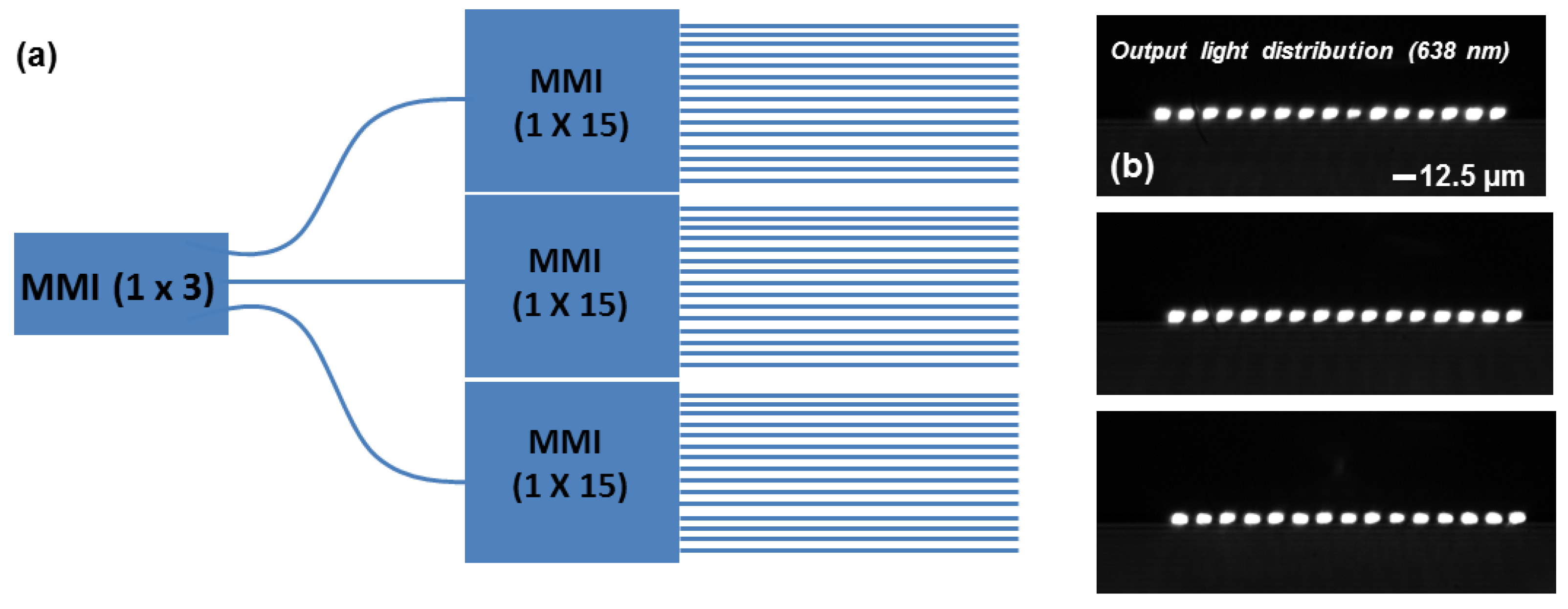
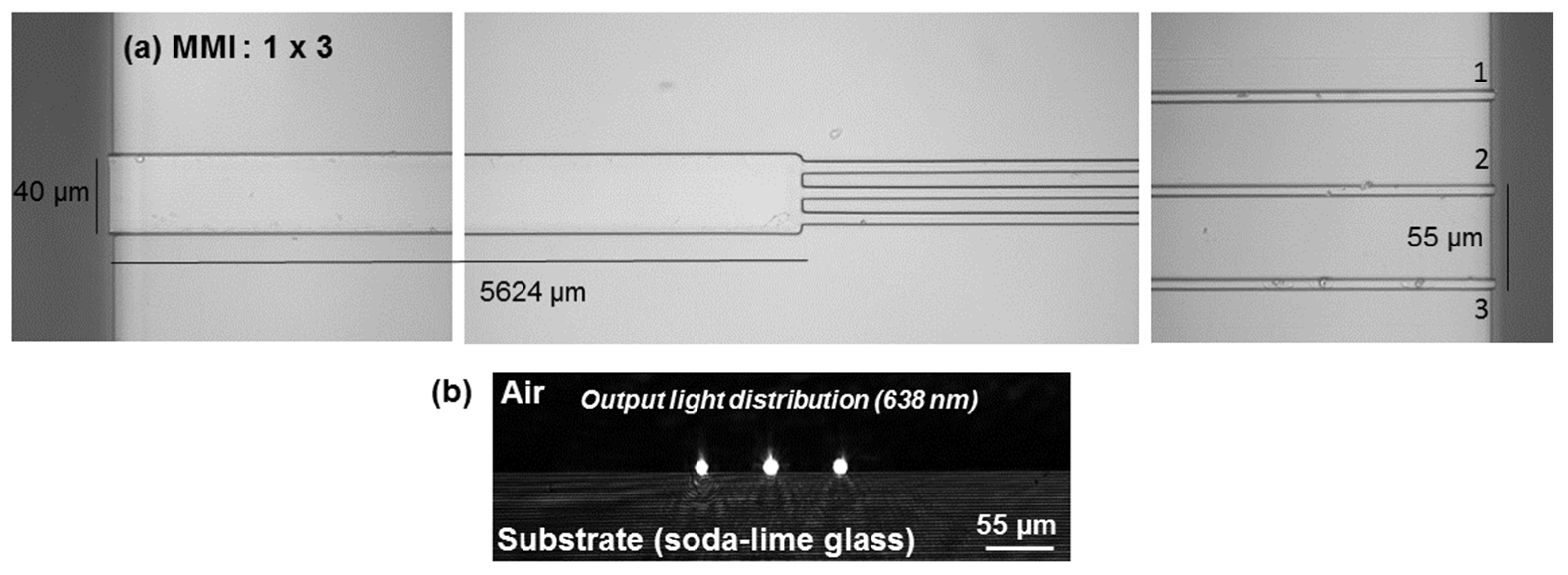
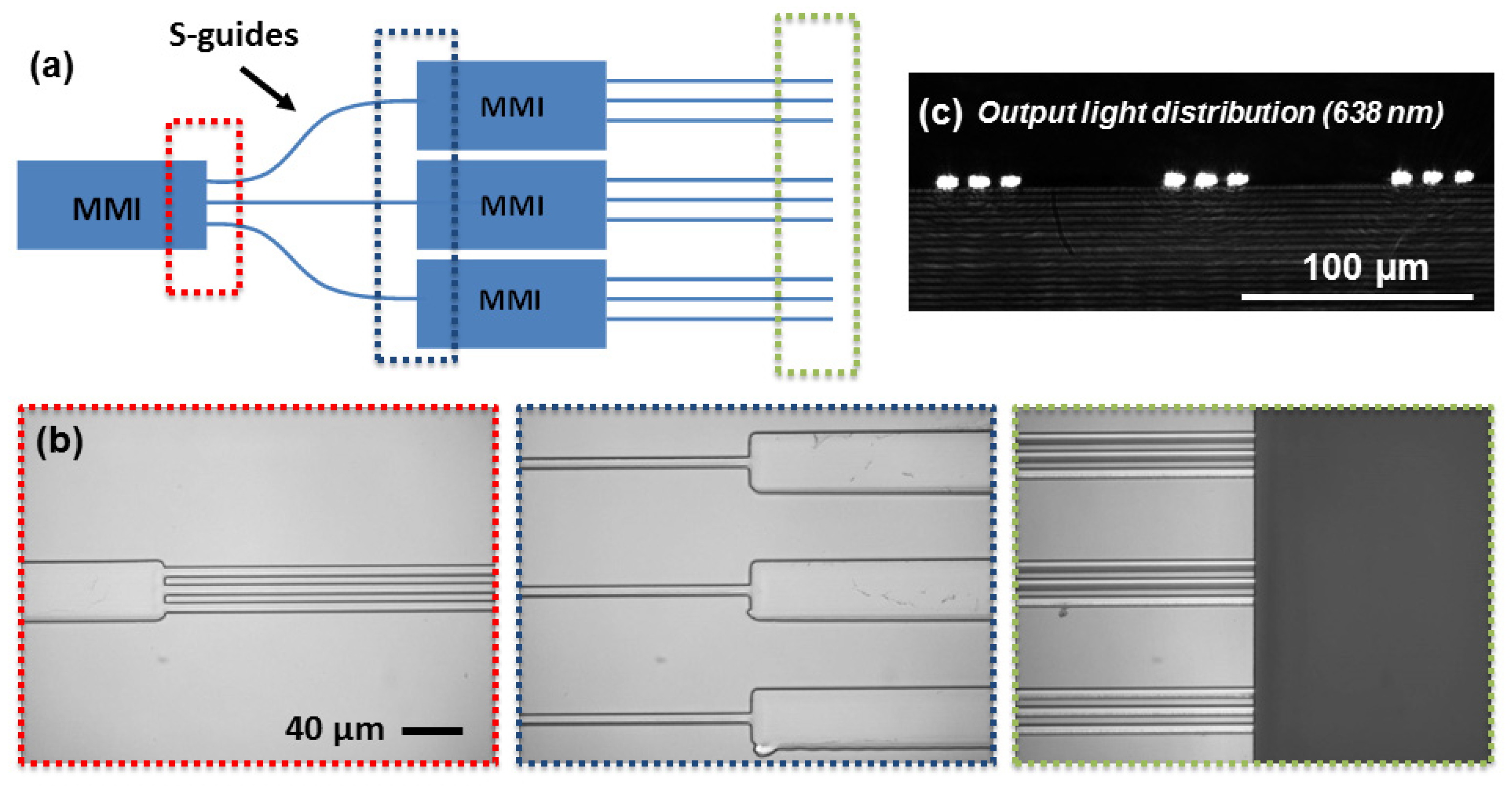
3.5. Creation of 1 × 3 and 1 × 9 MMI Couplers

The 1 × 3 MMI coupler, whose dimensions were defined using the simulation approach in Section 3.3, was experimentally manufactured. To this aim, the MMI coupler was created by the direct laser writing approach using a laser power of 70% and a scanning speed of 200 µm/s, while the OD of 1.72 was placed along the optical path. In order to ensure a flat, small roughness and a uniform surface, the FF was set at 75%, as evidenced in Section 3.4. The photoinduced device (top-view) is presented in Figure 9a, where a microscopic image is given illustrating the input (left), the transition from MMI to waveguides (center), and the three output waveguides (right). We can clearly see a satisfying match between the simulation and the experimental procedure: the same exact architecture can be created with a 40 µm × 5624 µm rectangular shape, while a distance of 12.5 µm between two adjacent waveguides is achieved. The fact that the distance between each waveguide is more important at the end of the device (55 µm) is related to a positive and negative 0.12° tilt for waveguides 1 and 3, respectively. We can also observe that both ends (input and output) are perfectly cleaved, allowing for the optimization of light injection and collection. The guiding properties of this coupler were also investigated after excitation at 638 nm using the experimental setup described in Section 2.3, and the result is represented in Figure 9b. We can clearly observe that with one single injection source (SMF28 fiber), it is possible to probe the three waveguides, as predicted through simulations. Intense optical light spots were experimentally observed at the outputs of the device.
The output light observation reveals a key point: despite the multiplication of probed waveguides, an important amount of light can still be detected. This opens the way for increasing the number of TiO2–SiO2 guides monitored by a single source. To this aim, we have manufactured a more complex architecture allowing us to probe more waveguides, as presented in Figure 10a. This architecture results from the combination of four MMI couplers (1 × 3), whose dimensions (40 µm × 5624 µm) are similar to the one illustrated in Figure 9. A 1 × 3 coupler splits the optical power into a straight waveguide and two curved waveguides (S-guides), whose length and bending radius are 6.8 mm and 125 mm, respectively. Each waveguide probes three similar MMI couplers (1 × 3), resulting in nine outputs. Microscopic images can also be observed in Figure 10b in order to have a better visualization of the manufactured device. The first 1 × 3 MMI, which was probed with an SMF28, is represented on the left, while particular attention is given to the transition from three waveguides to three couplers (center). Finally, the nine output TiO2–SiO2 waveguides are imaged on the right. Output optical light observation at 638 nm was performed on this architecture, as presented in Figure 10c, thus evidencing the possibility of probing nine waveguides with a single source. Interestingly, it should be noted that the signal seems to be quite similar in all the observed optical spots, despite the presence of two curved waveguides.

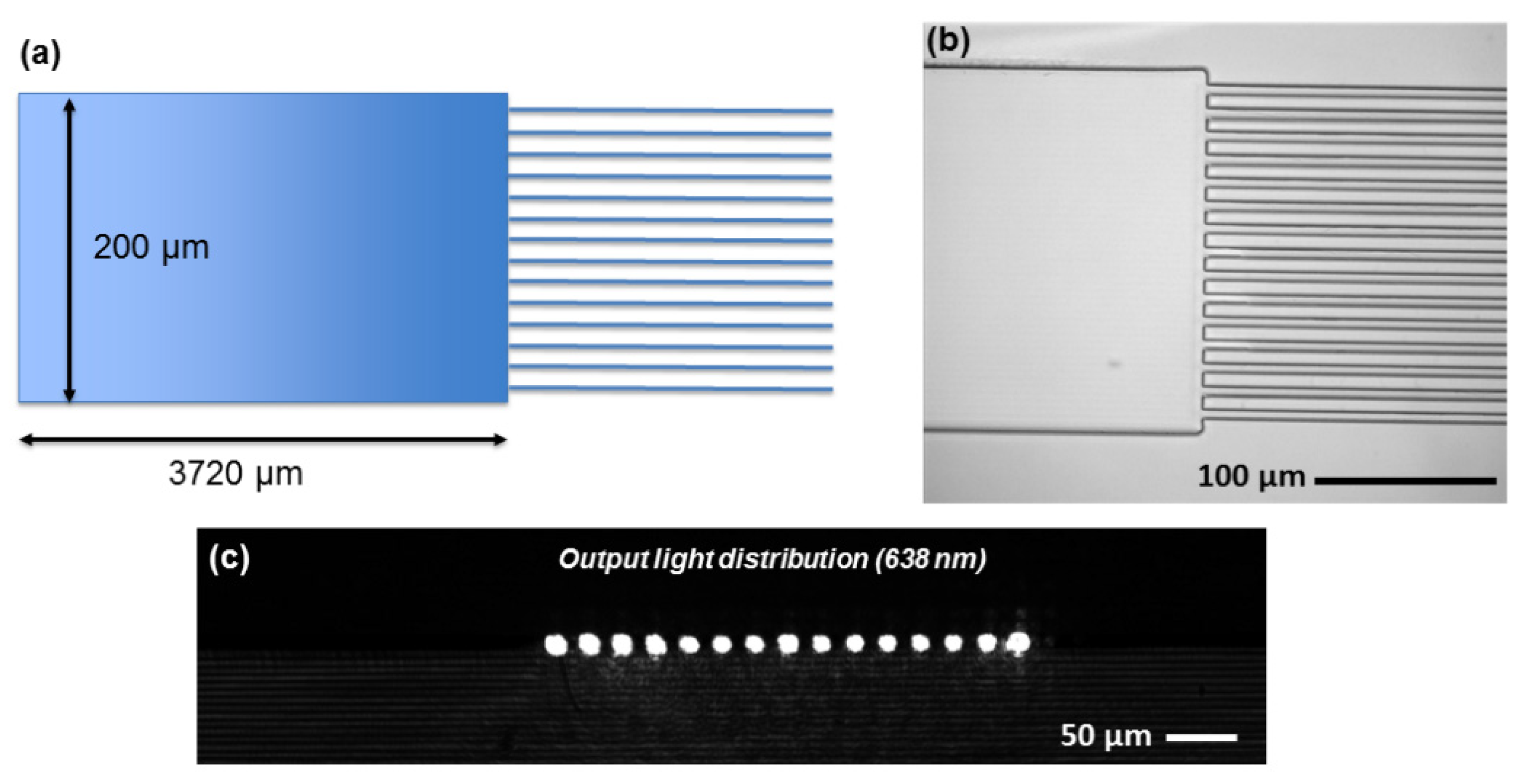
3.6. Toward the Development of More Compact Architectures (1 × 45)

This section is dedicated to the optimization of the 1 × 9 MMI splitter detailed in Figure 10, namely in terms of the number of waveguides probed by a single source. This optimization can be achieved by replacing the last three MMI (1 × 3) couplers (Figure 10) with three alternative structures, allowing for the probing of more sol-gel guides. First of all, we created another compact MMI coupler allowing us to probe 15 waveguides whose architecture was adapted and arranged from other authors [16]. The results are presented in Figure 11, where a scheme and a microscopic image are given in (a) and (b), respectively. The corresponding structure is a 200 µm × 3720 µm rectangular MMI coupler, splitting the optical power into a series of 15 straight waveguides separated by a 12.5 µm distance. The creation of this structure is still achieved using the direct laser writing approach with the same exact parameters (laser power, scanning speed, FF) defined in Section 3.4. Despite the high number of probed waveguides, the output optical power at 638 nm, represented in Figure 11c, remains intense for each waveguide.
As the ultimate goal is the functionalization of large surfaces such as aircraft wings, it is essential to investigate how to massively increase the number of sol-gel guides probed by a unique source. The latest resulting component, illustrated in Figure 12a, is a cascade between a first 1 × 3 MMI (40 µm × 5624 µm) coupler to three structures (1 × 15). Under this condition, 45 potential TiO2–SiO2 waveguides can be monitored. It should be noted that the bending radius of the S-guides is the same compared with the former 1 × 9 structure (125 mm), while their lengths are 11.6 mm. Finally, under excitation at 638 nm, as shown in Figure 12b, the organo-mineral circuit definitely reveals its efficiency by successfully probing 45 waveguides using one light source, allowing the use of more compact devices. Additionally, the division of light can be obtained after short distances, since the total length of the device is as low as 3 cm, increasing the possibility of integration in the aerospace domain.

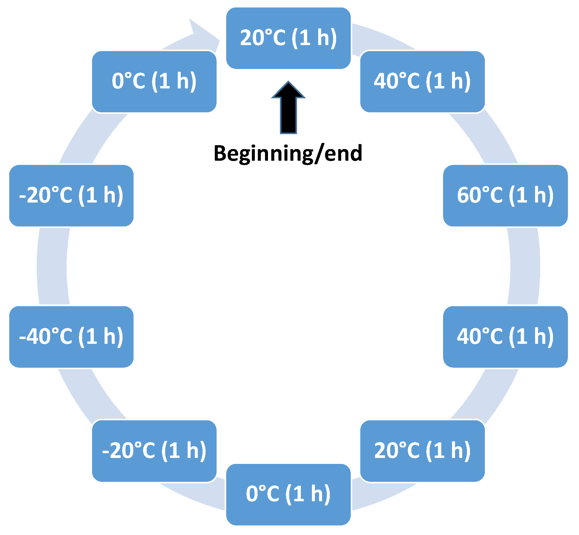
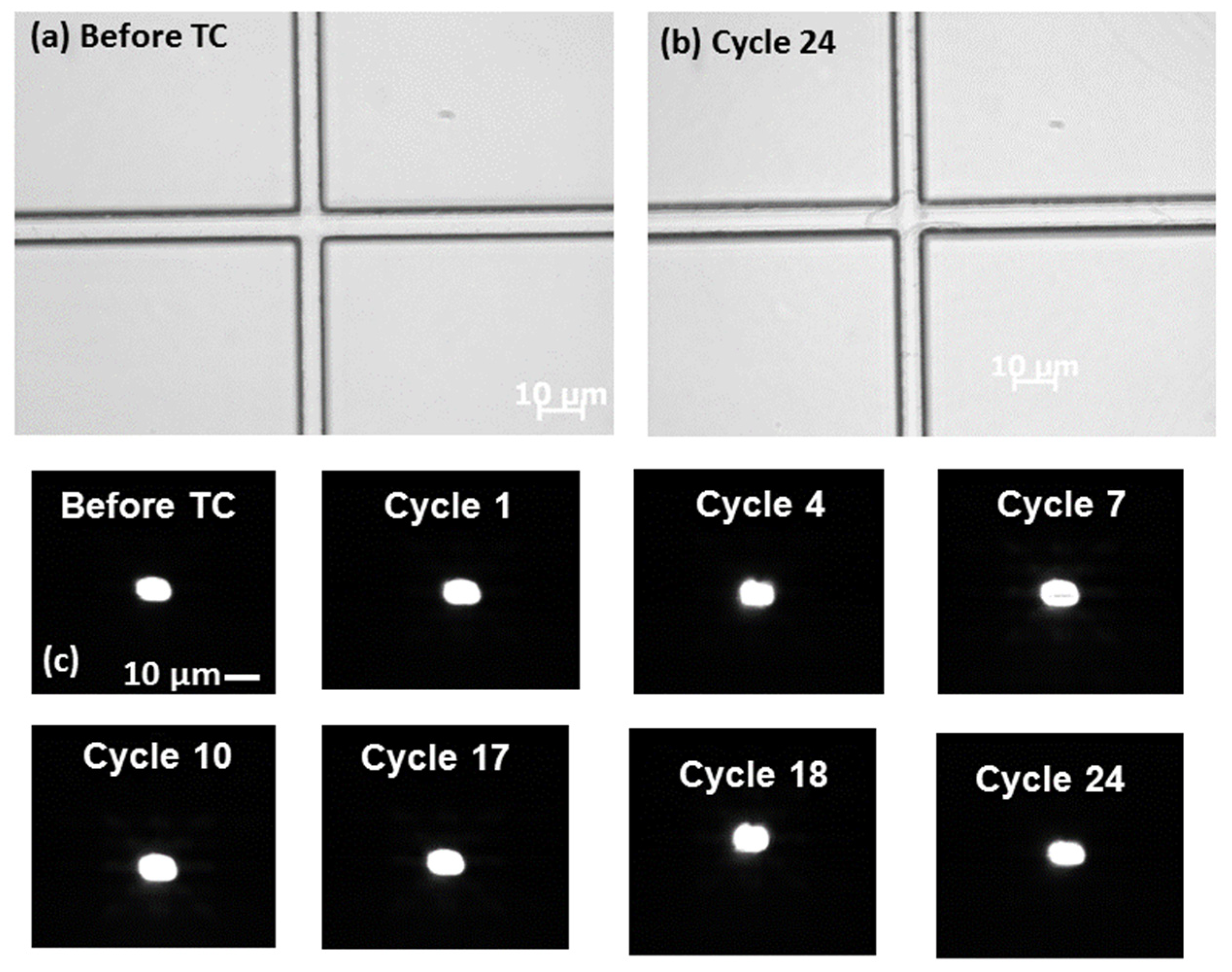
3.7. Behavior of TiO2–SiO2 Waveguides with Respect to Several Thermal Cycles

Since this sensor will be operational in the aerospace domain, namely in the civil aviation industry, it is crucial to check the impact of the TiO2–SiO2 architectures under extreme temperature changes. Aircraft are usually located near the tropopause, in the lower stratosphere (10–15 km), while cruising [23], leading to dramatic temperature variations from the ground temperature to roughly −50 °C. In [10], we evidenced the satisfying mechanical resistance of TiO2–SiO2 waveguides for one thermal cycle (TC) with extreme temperatures ranging from 80 °C to −40 °C, showing that no dilation is induced while the guide structure remains unaffected. However, the impact of the thermal cycle on the light guidance was not investigated. To this aim, a deeper investigation was performed on a series of 24 TCs from 60 °C to −40 °C on two sets of samples: the first corresponds to a 10 cm × 10 cm grid, while the second is related to straight waveguides dedicated to optical light observations. The selected TC is depicted in Figure 13. Once placed in the oven, samples are exposed to three consecutive steps: an initial temperature increase from 20 °C to 60 °C, followed by a decrease to −40 °C, while a final increase up to 20 °C concludes the TC. It should be mentioned that each temperature level lasts 1 h, while a ramp of 1 °C/min is applied between two consecutive temperatures.
First of all, after each TC, microscope observations of a waveguide grid were recorded. Figure 14a presents an image of the sol-gel device, namely a crossed area, before being submitted to the first TC. A series of 24 cycles were performed on the same grid, and the final architecture is presented in Figure 14b. Despite the cumulative number of cycles, the structure was not altered by dramatic temperature changes from 60 °C to −40 °C, where no shrinkages, dilations, or fatigue cracks occurred. It should be remembered that the 10 cm × 10 cm waveguide grid is composed of 30 sol-gel waveguides separated by a 5 mm distance, resulting in 3 m of TiO2–SiO2 guides. After investigation of all the grid architectures, we did not observe any damage across all TCs, definitively evidencing that this sensor based on sol-gel devices is very promising for aerospace applications in terms of mechanical resistance, where important temperature variations can occur. In addition to microscopic observations, the output light of straight waveguides (thickness: 5 µm and width: 9 µm) was recorded after each TC in order to identify the potential impact of negative temperatures on the guiding properties. They were obtained under excitation with a supercontinuum source, emitting photons in the 350 nm–2000 nm range, and the results are synthesized in Figure 14c. The output light of a sol-gel guide is firstly recorded before being placed in the oven, revealing an intense light collection, as expected. Interestingly, it should be noted that the light propagation seems to be unaffected by a cumulative number of cycles (1, 4, 7, 10, 17, 18, 24), where excellent light transport is still achieved even with the highest number of cycles (24) used in the experiment. In Figure 14c, we have only presented the results regarding a single waveguide. However, this latter is representative of all the waveguides investigated in this work insofar as optical light observations reveal that none of the waveguides were affected by temperature changes. Through this particular study, the sol-gel structures appeared to show no sign of material fatigue or wear (mechanical resistance and light guidance), despite aggressive environmental conditions up to 24 cycles. Even if these results are a good indicator, more tests need to be performed to predict the lifespan of sol-gel architectures and a dedicated test campaign should be performed to validate this aspect. For instance, it is possible to increase the ramp applied between two consecutive temperatures and the number of cycles, while representative aircraft panels can be used as a substrate.

4. Conclusions

In the framework of the ADD-ON project (Clean Sky 2, H2020), an optimization of a 2D sol-gel waveguide sensor based on light transport for damage detection in the aerospace domain was presented. This work is mainly related to the optimization of the number of TiO2–SiO2 guides that can be probed from a unique optical source. Our main goal was to obtain access to more compact sensors based on MMI effects and the self-imaging principle. A BPM simulation approach was first selected in order to design a rectangular MMI coupler (40 µm × 5624 µm), allowing us to split the injected light in the visible domain (600 nm) equally between three waveguides. The manufacturing of the conceived device was achieved using the direct laser writing approach. After the injection of light into this optimized component, three intense optical spots were observed at the device’s output, confirming the simulative approach. Based on this architecture, we have created more complex and exotic TiO2–SiO2 MMI couplers, allowing for the probing of 9, 15, or 45 waveguides with a single optical source. The output light observations provide clear evidence of a satisfying light collection despite the multiplication of waveguides and the presence of curved waveguides between the various MMI device subparts. Additionally, a deeper investigation regarding temperature effects on the waveguide properties, representative of the ones induced during aircraft cruising, were performed using 2D and straight TiO2–SiO2 sol-gel waveguides. After being submitted to 24 consecutive thermal cycles from 60 °C to −40 °C, the structures remained unchanged, since no cracks were induced, while their optical guiding properties remained unaltered, providing sufficiently large intense light for our sensor operation principle. Even if this particular temperature study is a satisfying indicator at this stage, more tests need to be performed in order to validate this aspect. The fact that a single source may monitor several guides simultaneously can be exploited to produce more compact, less intrusive, and lower-cost sensors, thus fulfilling SHM requirements in the aerospace domain. Finally, this architecture will be implemented into a 2D matrix configuration, while preliminary results concerning the functionalization of aircraft panels with sol-gel show that it can be easily spread and a satisfying adherence is possible without any preparation of the panel substrate. Further investigations are in progress regarding this aspect.

Author Contributions

Conceptualization, M.R., T.B., M.A., D.J., E.M., M.-A.D.S., K.A. and S.G.; methodology, M.R., T.B., M.A., F.V., D.J., F.R., E.M., A.M. and S.G.; software, T.B. and D.J.; validation, M.R., T.B., F.V., Y.J., R.E., T.V.L., A.W., M.-A.D.S., K.A. and S.G.; formal analysis, M.R. T.B., M.A. and D.J.; investigation, M.R., T.B., M.A., D.J., E.M., A.M., R.E., T.V.L., A.W., M.-A.D.S., K.A. and S.G.; resources, D.J., F.R., F.V., A.B., Y.O., Y.J. and S.G.; data curation, D.J.; writing—original draft preparation, M.R. and T.B.; writing—review and editing, M.R., T.B., D.J., F.R., F.V., E.M., A.M., Y.O., Y.J., R.E., T.V.L., A.W. and S.G.; visualization, M.R. and T.B.; supervision, Y.J., M.-A.D.S., K.A. and S.G.; project administration, M.-A.D.S., K.A. and S.G.; funding acquisition, R.E. and S.G. All authors have read and agreed to the published version of the manuscript.

Funding

This project has received funding from the Clean Sky 2 Joint Undertaking under the European Union’s Horizon 2020 research and innovation program under grant agreement n°785341.

Institutional Review Board Statement

Not Applicable.

Informed Consent Statement

Not Applicable.

Data Availability Statement

Not Applicable.

Acknowledgments

This work was partly supported by the French RENATECH+ network led by the CNRS on the NanoSaintEtienne platform.

Conflicts of Interest

The authors declare no conflict of interest.

References

  1. Güemes, A.; Fernandez-Lopez, A.; Pozo, A.R.; Sierra-Pérez, J. Structural Health Monitoring for Advanced Composite Struc-tures: A Review. J. Compos. Sci. 2020, 4, 13–27. [Google Scholar] [CrossRef] [Green Version]
  2. Bezas, K.; Komianos, V.; Koufoudakis, G.; Tsoumanis, G.; Kabassi, K.; Oikonomou, K. Structural Health Monitoring in His-torical Buildings: A Network Approach. Heritage 2020, 3, 796–818. [Google Scholar] [CrossRef]
  3. Kumberg, T.; Schneid, S.; Reindl, L. A Wireless Sensor Network Using GNSS Receivers for a Short-Term Assessment of the Modal Properties of the Neckartal Bridge. Appl. Sci. 2017, 7, 626. [Google Scholar] [CrossRef] [Green Version]
  4. Dong, T.; Kim, N.H. Cost-Effectiveness of Structural Health Monitoring in Fuselage Maintenance of the Civil Aviation Industry. Aerospace 2018, 5, 87. [Google Scholar] [CrossRef] [Green Version]
  5. Bhuiyan, M.Y.; Giurgiutiu, V. Multiphysics Simulation of Low-Amplitude Acoustic Wave Detection by Piezoelectric Wafer Active Sensors Validated by In-Situ AE-Fatigue Experiment. Materials 2017, 10, 962–979. [Google Scholar] [CrossRef] [PubMed] [Green Version]
  6. Smithard, J.; Rajic, N.; Van Der Velden, S.; Norman, P.; Rosalie, C.; Galea, S.; Mei, H.; Lin, B.; Giurgiutiu, V. An Advanced Multi-Sensor Acousto-Ultrasonic Structural Health Monitoring System: Development and Aerospace Demonstration. Mater. 2017, 10, 832. [Google Scholar] [CrossRef] [Green Version]
  7. Di Sante, R. Fibre Optic Sensors for Structural Health Monitoring of Aircraft Composite Structures: Recent Advances and Applications. Sensors 2015, 15, 18666–18713. [Google Scholar] [CrossRef]
  8. Lee, B.H.; Kim, Y.H.; Park, K.S.; Eom, J.B.; Kim, M.J.; Rho, B.S.; Choi, H.Y. Interferometric Fiber Optic Sensors. Sensors 2012, 12, 2467–2486. [Google Scholar] [CrossRef] [PubMed] [Green Version]
  9. Takeda, N.; Okabe, Y.; Mizutani, T. Damage detection in composites using optical fibre sensors. Proc. Inst. Mech. Eng. Part G J. Aerosp. Eng. 2007, 221, 497–508. [Google Scholar] [CrossRef]
  10. Royon, M.; Jamon, D.; Blanchet, T.; Royer, F.; Vocanson, F.; Marin, E.; Morana, A.; Boukenter, A.; Ouerdane, Y.; Jourlin, Y.; et al. Sol–Gel Waveguide-Based Sensor for Structural Health Monitoring on Large Surfaces in Aerospace Domain. Aerosp. 2021, 8, 109. [Google Scholar] [CrossRef]
  11. Hench, L.L.; West, J.K. The Sol-Gel Process. Chem. Rev. 1990, 90, 33–72. [Google Scholar] [CrossRef]
  12. Jerónimo, P.C.; Araújo, A.N.; Montenegro, M. Optical sensors and biosensors based on sol–gel films. Talanta 2007, 72, 13–27. [Google Scholar] [CrossRef] [PubMed]
  13. Gelover, S.; Mondragón, P.; Jiménez, A. Titanium Dioxide Sol-Gel Deposited Over Glass and Its Application as a Photocatalyst for Water Decontamination. J. Photochem. Photobiol. A 2003, 165, 241–246. [Google Scholar] [CrossRef]
  14. Oubaha, M.; Kribich, R.K.; Copperwhite, R.; Etienne, P.; O’Dwyer, K.; MacCraith, B.D.; Moreau, Y. New Inorganic Sol-Gel Material with High Transparency at 1.55 µm. Opt. Commun. 2005, 253, 346–351. [Google Scholar] [CrossRef]
  15. Coudray, P.; Etienne, P.; Moreau, Y. Integrated optics based on organo-mineral materials. Mater. Sci. Semicond. Process. 2000, 3, 331–337. [Google Scholar] [CrossRef]
  16. Fardad, M.; Mishechkin, O.; Fallahi, M. Hybrid sol-gel materials for integration of optoelectronic components. J. Light. Technol. 2001, 19, 84–91. [Google Scholar] [CrossRef]
  17. Royon, M.; Vocanson, F.; Jamon, D.; Marin, E.; Morana, A.; Boukenter, A.; Girard, S.; Ouerdane, Y.; Royer, F.; Jourlin, Y. Comparison between the UV and X-ray Photosensitivities of Hybrid TiO2-SiO2 Thin Layers. Materials 2020, 13, 3730–3739. [Google Scholar] [CrossRef]
  18. Soldano, L.B.; Pennings, E.C.M. Optical multi-mode interference devices based on self-imaging: Principles and applications. J. Light. Technol. 1995, 13, 615–627. [Google Scholar] [CrossRef] [Green Version]
  19. Bachmann, M.; Besse, P.A.; Melchior, H. General Self-Imaging Properties in N x N Multimode Interference Couplers Including Phase Relations. Appl. Opt. 1994, 33, 3905–3911. [Google Scholar] [CrossRef]
  20. Hill, M.M.; Leijtens, X.; Khoe, G.G.-D.; Smit, M.M. Optimizing imbalance and loss in 2 x 2 3-db multimode interference couplers via access waveguide width. J. Light. Technol. 2003, 21, 2305–2313. [Google Scholar] [CrossRef]
  21. Franc, J.; Blanc, D.; Zerroukhi, A.; Chalamet, Y.; Last, A.; Destouches, N. Organo-silica–titania nanocomposite elaborated by sol–gel processing with tunable optical properties. Mater. Sci. Eng. B 2006, 129, 180–185. [Google Scholar] [CrossRef]
  22. Royon, M.; Vocanson, F.; Jamon, D.; Royer, F.; Marin, E.; Morana, A.; Campanella, C.; Boukenter, A.; Ouerdane, Y.; Jourlin, Y.; et al. Impact of γ-rays Irradiation on Hybrid TiO2-SiO2 Sol-Gel Films Doped with RHODAMINE 6G. Materials 2021, 14, 5754–5765. [Google Scholar] [CrossRef] [PubMed]
  23. Ștefan, S.; Antonescu, B.; Urlea, A.; Buzdugan, L.; Andrei, M.; Necula, C.; Voinea, S. Study of Clear Air Turbulence Related to Tropopause Folding over the Romanian Airspace. Atmosphere 2020, 11, 1099. [Google Scholar] [CrossRef]
Figure 1. Two-dimensional sol-gel matrix sensor for damage or delamination detection. (a) Sensor principle where damage leads to the rupture of one or several TiO2–SiO2 guides. Its localization can be deduced thanks to the 2D structure. (b) Example of a 2D grid waveguide obtained on soda-lime substrate glass. (c) TiO2–SiO2 grid observed with an optical microscope. This figure is adapted from [10].
Aerospace 08 00401 g001
Figure 2. Setup used for the light injection (top-view). An SMF28 fiber is placed in a V-groove platform and fixed with magnets. The light injection, performed through a butt-coupling configuration, is optimized by moving the fiber in the X, Y, and Z directions. A camera (not shown here) records the top-view (XZ-plane) for optimal light injection while a second camera (on the right) is used for imaging the output light of the TiO2–SiO2 sol-gel waveguides.
Aerospace 08 00401 g002
Figure 3. Schematic of the different designs computed with the BPM. (a) YZ-plane representing the TiO2–SiO2 waveguide (n = 1.58) deposited on soda-lime glass (n = 1.52) and surrounded by air (n = 1). (b) Corresponding XZ-plane (top-view). (c) Modeling of the 1 × 3 MMI coupler (top-view) with a fixed width of 40 µm. In any case, all simulations were performed at 600 nm. The laser is injected through a butt-coupling approach using an SMF28 optical fiber.
Aerospace 08 00401 g003
Figure 4. Microscope observation (top view) obtained in reflection mode (×63) for (a) a waveguide written using a low scanning speed (lateral dimension = 20 µm) and (b) a higher scanning speed (lateral dimension = 10 µm). (c) Corresponding profilometer measurements. Output light distribution at 638 nm for the (d) 20 µm and (e) 10 µm waveguides, respectively. In any case, the blue line is related to the 20 µm waveguide in width while the red color refers to the 10 µm one.
Aerospace 08 00401 g004
Figure 5. Spatial distribution in the XY-plane of the output light intensity from a waveguide (4 µm × 8 µm) at 600 nm under excitation with an SMF28 (butt-coupling configuration) for different X-axis misalignments of: (a) 0 µm (perfect case), (b) 1 µm, (c) 4 µm, and (d) 8 µm.
Aerospace 08 00401 g005
Figure 6. BPM simulation (at 600 nm) of the light field propagation along a strongly multi-mode waveguide (width: 40 µm) in the XZ-plane. Self-imaging can be observed for one or three images at periodic intervals along the Z-axis. The waveguide is excited by an SMF28 optical fiber (left) through a butt-coupling configuration.
Aerospace 08 00401 g006
Figure 7. (a) BPM simulation (at 600 nm) of light field propagation along a 40 µm × 5624 µm MMI coupler, allowing for the simultaneous probing of 3 waveguides with an SMF28 (XZ-plane). (b) Corresponding output light distribution (XY-plane) where the distance between two consecutive waveguides is 12.5 µm.
Aerospace 08 00401 g007
Figure 8. Influence of the filling factor (FF), ranging from 0% to 75% on the shape of TiO2–SiO2 MMI-like structures (square shape and three waveguides with a 6 µm lateral dimension). (a) Microscope images (× 40) of an MMI-like structure obtained with an FF of 0%, (b) corresponding profile, (c) MMI at an FF of 50%, (d) corresponding profile, (e) MMI at an FF of 75%, and (f) corresponding profile.
Aerospace 08 00401 g008
Figure 9. (a) Microscopic observation of a 1 × 3 MMI coupler obtained by micro-structuration of a TiO2–SiO2 layer. (b) Output light intensity distribution under excitation at 638 nm.
Aerospace 08 00401 g009
Figure 10. (a) Overview of the photonic device composed of 4 MMI couplers (1 × 3): one source can monitor 9 waveguides. (b) Microscopic images of the device, showing the end of the first MMI coupler (left), the transition from waveguides to 3 MMI couplers (center), and the 9 output waveguides (right). (c) Corresponding output light distribution under excitation at 638 nm.
Aerospace 08 00401 g010
Figure 11. A 1 × 15 MMI sol-gel coupler obtained by direct laser writing technique. (a) Overview of the splitter. (b) Corresponding microscopic image and (c) output light at 638 nm under excitation with an SMF28. The coupler corresponds to a 200 µm × 3720 µm rectangular structure.
Aerospace 08 00401 g011
Figure 12. A 1 × 45 MMI coupler. (a) Overview of the MMI. (b) Output light distribution under excitation at 638 nm.
Aerospace 08 00401 g012
Figure 13. Description of the thermal cycle performed on TiO2–SiO2 architectures between two extreme temperatures: 60 °C and −40 °C. Each temperature level lasts 1 h, while a ramp of 1 °C/min is applied between two consecutive values.
Aerospace 08 00401 g013
Figure 14. Influence of 24 thermal cycles on TiO2–SiO2 sol-gel waveguides. Microscope observations of a waveguide grid (a) before the thermal cycle and (b) after 24 cycles. (c) Output light observations after injection of white light (supercontinuum) in straight waveguides after several thermal cycles.
Aerospace 08 00401 g014
Table 1. Effect of the X-axis misalignment (0 µm, 1 µm, 4 µm, 8 µm) on the connection losses between SMF28 and TiO2–SiO2 waveguides at 600 nm.
Waveguide Width (µm)X-Axis Misalignment (µm) Connection Losses (%)
10015
10115
10435
10895
30015
Publisher’s Note: MDPI stays neutral with regard to jurisdictional claims in published maps and institutional affiliations.

