


Improvement of β-SiC Synthesis Technology on Silicon Substrate
by
 , , , and
Yana Suchikova
1,* ,
,
Sergii Kovachov
1,
Ihor Bohdanov
1,
Artem L. Kozlovskiy
2,3,
Maxim V. Zdorovets
2,3 and
Anatoli I. Popov
2,4,* 1
The Department of Physics and Methods of Teaching Physics, Berdyansk State Pedagogical University, 71100 Berdyansk, Ukraine
2
Engineering Profile Laboratory, L.N. Gumilyov Eurasian National University, Satpaev Str. 5, Astana 010008, Kazakhstan
3
Laboratory of Solid State Physics, Institute of Nuclear Physics, Almaty 050032, Kazakhstan
4
Institute of Solid State Physics, University of Latvia, 8 Kengaraga Str., LV-1063 Riga, Latvia
*
Authors to whom correspondence should be addressed.
Technologies 2023, 11(6), 152; https://doi.org/10.3390/technologies11060152
Submission received: 23 September 2023
/
Revised: 19 October 2023
/
Accepted: 19 October 2023
/
Published: 27 October 2023
(This article belongs to the Special Issue Advanced Processing Technologies of Innovative Materials)
Abstract
:This article presents an enhanced method for synthesizing β-SiC on a silicon substrate, utilizing porous silicon as a buffer layer, followed by thermal carbide formation. This approach ensured strong adhesion of the SiC film to the substrate, facilitating the creation of a hybrid hetero-structure of SiC/por-Si/mono-Si. The surface morphology of the SiC film revealed islands measuring 2–6 μm in diameter, with detected micropores that were 70–80 nm in size. An XRD analysis confirmed the presence of spectra from crystalline silicon and crystalline silicon carbide in cubic symmetry. The observed shift in spectra to the low-frequency zone indicated the formation of nanostructures, correlating with our SEM analysis results. These research outcomes present prospects for the further utilization and optimization of β-SiC synthesis technology for electronic device development.
1. Introduction
Silicon has long been the primary material for solar energy applications, largely owing to its natural abundance and low toxicity [1,2]. However, recent studies have highlighted certain limitations in the energy conversion efficiency of silicon-based photovoltaic cells [3,4], catalyzing the exploration of alternative semiconducting materials. In this vein, semiconductors such as cadmium telluride (CdTe) [5,6], gallium arsenide (GaAs) [7,8], indium phosphide (InP) [9,10], and complex ternary compounds like CdxTeyOz [11,12], AlxGa1−xAs [13,14], and CuGaxIn1−xSe2 [15,16] have garnered significant attention. Despite the promising attributes of these materials, they are often compromised by high production costs [17]. To ameliorate this, nanostructuring the surfaces of these semiconductors has been suggested as a method to enhance their light absorption coefficients [18,19,20]. Nonetheless, the scarcity of elements like indium and gallium restricts the large-scale application of such materials to space-based solar cells [21,22], emphasizing the need for efficient and cost-effective materials for terrestrial use.
Emerging as a viable option is silicon carbide (SiC), a material comprising silicon and carbon, two of Earth’s most abundant elements [23,24,25]. The well-characterized semiconductor properties of SiC make it conducive for industrial-scale utilization [26,27,28,29,30,31,32,33,34,35], akin to silicon. In addition to its robust thermal conductivity, electric breakdown voltage, and current density, SiC can operate over a broad temperature range without undergoing degradation in its monocrystalline structure or phase transitions. Through doping, the semiconductor properties of SiC can be tailored to yield both n-type and p-type materials [36,37]. These defects have been reported to impede the electrical and mechanical properties of the material, as corroborated by extensive studies [38,39]. Such defects are not just distinctive to silicon carbide but are a recurring theme across the broader category of semiconductors, each requiring its unique set of mitigative strategies.
Another formidable obstacle lies in the lattice mismatch when SiC films are grown on non-lattice-matched substrates. The repercussions of this discrepancy are often the formation of strain-induced defects that can severely compromise the crystalline quality of SiC films, thereby limiting their applicability in electronic devices [40,41].
To ameliorate these complexities, prior research has established the efficacy of incorporating intermediate buffer layers as a palliative measure [42,43]. Notably, porous domains or interstitial spaces generated on the semiconductor surface via electrochemical procedures have been shown to serve as effective buffer layers, considerably reducing defect densities and lattice mismatch-induced stresses [44,45,46]. Additionally, it has been demonstrated repeatedly that the nanostructuring of silicon leads to a change in the properties of the monocrystalline counterpart, allowing for a significant improvement in the characteristics of solar cells fabricated based on it [47,48,49].
The present study introduces a cost-effective approach for synthesizing high-quality β-SiC films on silicon substrates, utilizing a porous silicon (por-Si) intermediary buffer layer.
Using the electrochemical etching technique, the methodology begins by establishing a porous layer on the monocrystalline silicon surface. This method possesses distinct economic advantages such as reduced material wastage, lower energy consumption, and a minimal requirement of specialized equipment. Furthermore, the electrochemical etching process can be precisely controlled to produce uniform pores, thus reducing the need for additional post-processing or treatments. Considering these benefits, electrochemical etching can be up to 40–60% more cost-effective compared to other pore-formation methods.
The subsequent growth of SiC is facilitated by rapid thermal vacuum carbonization. Including the buffer porous layer is pivotal for attaining a pristine silicon carbide film.
Regarding material safety, both silicon and silicon carbide stand out for their benign nature. Silicon, a primary component of the Earth’s crust, is non-toxic and abundantly available. Silicon carbide, similarly, is considered environmentally friendly and non-toxic compared to other semiconductors that are frequently employed in solar cells, such as cadmium telluride or copper indium gallium selenide, which have raised environmental and health concerns. This inherent non-toxicity of the β-SiC/por-Si/mono-Si heterostructure materials emphasizes their suitability for sustainable and eco-friendly solar cell applications.
Given the economic and environmental merits, the β-SiC/por-Si/mono-Si heterostructure demonstrates significant potential as an advanced and viable material for use in solar cell applications. The novelty of our work lies in using a porous buffer layer, which not only facilitates the growth of high-quality silicon carbide films but also enhances the adhesion and structural integrity of the resulting heterostructure. Consequently, this new approach reduces production costs and yields a high-quality heterostructure with excellent electronic properties, making the β-SiC/por-Si/mono-Si heterostructure a promising material for application in solar cells.
2. Materials and Methods
2.1. Samples for the Experiment
A monocrystalline Si of n-type conductivity was utilized for the experiment, doped with phosphorus to a concentration of 1.8 × 1017 cm−1. Plates oriented as (111) with dimensions of 1 × 2 × 0.2 cm were employed.
2.2. Electrolytes, Precursors, and Equipment
For the electrochemical modification of the silicon substrate, an initial step involved the removal of the native oxide passivating layer. This procedure was accomplished through electrochemical etching using a hydrochloric acid (HCl) solution. The experimental setup included a standard three-electrode electrochemical cell. Within this configuration, a platinum electrode served as the counter electrode, while a silver–silver chloride electrode acted as the reference.
To augment the efficiency of the etching process, the electrochemical cell was equipped with two additional subsystems. Firstly, an air-blowing module was incorporated to eliminate the formation of oxygen bubbles on the sample surface that could otherwise hinder the etching process. Second, an electrolyte stirring mechanism was added to ensure uniform electrolyte distribution and consistent etching across the substrate.
After removing the oxide layer, the next phase involved the formation of a porous silicon layer. This was achieved through electrochemical etching in a hydrofluoric acid (HF) solution within the same electrochemical cell. The electrolyte was maintained at room temperature during this stage of the procedure. The etching was conducted under ambient lighting conditions and did not require specialized environmental controls.
Post-etching, the samples underwent a drying process within a SNOL 58/350 muffle furnace to remove any residual moisture and to prepare their surfaces for subsequent procedures.
Finally, the silicon carbide layer was synthesized using a Jipelec JetFirst-100 oven. A methane (CH4) gas precursor was deployed for this purpose, facilitating the formation of Si-C bonds and thereby culminating in the growth of a high-quality SiC layer.
All chemicals utilized were procured from Spetsprompostach LLC. The hydrochloric HCl and HF acids were of analytical grade (ARG, 99.8%), indicating a high purity level suitable for analytical applications and ensuring minimal interference from impurities during the electrochemical etching processes. The silicon (Si) substrate was of semiconductor grade, a designation for materials with controlled and specified impurity levels to ensure optimal electrical conductivity and functionality in semiconductor applications. Methane (CH4), which was utilized to synthesize the silicon carbide layer, was of ultra-high purity (UHP) grade with a purity level of 99.995%, ensuring the high-quality synthesis of the SiC layer.
2.3. Experiment Steps
The experiment was conducted in several stages, specifically:
- Stage 1—Formation of the porous Si layer;
- Stage 2—Removal of reaction products from the sample surface;
- Stage 3—Formation of the SiC layer;
- Stage 4—Post-processing of the samples.
Detailed experimental stages are provided below.
2.3.1. Stage 1. Electrochemical Etching in Acid Solutions
The preliminary phase of the experimental procedure focused on the meticulous preparation of the monocrystalline silicon (mono-Si) surface to render it amenable for silicon carbide (SiC) layer formation. A point of concern in semiconductor processing is the natural tendency of the silicon surface to oxidize following mechanical operations such as grinding and polishing. This oxidation forms a thin, amorphous oxide layer documented to expedite the device degradation rate and pose challenges in further fabrication steps [50,51]. Therefore, it is imperative to effectively remove this passivating oxide layer to preserve the monocrystalline silicon substrate’s intrinsic properties and facilitate subsequent process steps [52,53].
To further facilitate the quality of SiC films, a strategic approach involves formulating a textured or porous silicon layer on the monocrystalline silicon surface. These specially engineered buffer layers act as a soft substrate, addressing and alleviating the perennial lattice mismatch between the SiC film and the mono-Si substrate. The resulting architecture diminishes the manifestation of elastic stresses at the interface, thereby potentially enhancing the SiC films’ overall quality and reprehensive understanding and repeatability. The specific conditions under which this initial phase of the experiment was conducted are systematically documented in Table 1, while the accompanying Figure 1 provides a visual representation to aid interpretation.
A standard three-electrode cell ensemble was employed in the electrochemical etching process utilized for both the removal of oxide and the formation of a porous layer on the monocrystalline silicon substrate. In the initial sub-stage (1.1), a potential of 2V was applied for 3 min in a 5% HCl solution to facilitate the removal of the oxide layer. Subsequently, in the second sub-stage (1.2), the porous silicon layer was formed by applying a potential of 5V for 7 min in a 50% HF solution. This higher potential drove the electrochemical etching of the silicon substrate, inducing porosity. The specific current during these processes was not fixed but could fluctuate to maintain the set potential, ensuring that the desired electrochemical reactions occurred. The final sub-stage (1.3) involved rinsing the silicon substrate in water to remove any reaction products from the surface, setting the stage for subsequent procedures. Through this systematic electrochemical etching process, the silicon substrate was adequately prepared to synthesize the silicon carbide layer, addressing the inherent challenges associated with the lattice mismatch and the passivating oxide layer.
2.3.2. Stage 2. Removal of Moisture Residues and Reaction Products from the Sample Surface
The second stage of the experimental process was engineered to meticulously remove moisture residues and byproducts from the treated surface of the porous silicon (por-Si) sample. Such procedural steps are integral to ensure an uncontaminated substrate for subsequent silicon carbide (SiC) film formation. To achieve this, samples were subjected to a tightly controlled drying sequence in a SNOL 58/350 oven, characterized by three discrete sub-stages delineated by specific durations and temperatures as outlined in Table 2.
Table 2 comprehensively summarizes the conditions and sub-stages: starting with a 180-min treatment at 150 °C, followed by 60 min at 300 °C and then 400 °C. The judiciously selected time and temperature parameters were optimized to remove any vestigial moisture residues without adversely affecting the integrity of the por-Si substrate.
Initiating the SiC film formation immediately after this stage was paramount to mitigate the potential of the sample oxidation processes post-drying. Thus, the transition to the SiC film formation was executed without delay to maintain a contiguous processing flow.
2.3.3. Stage 3. Thermal Deposition and SiC Film Formation
Employing rapid thermal vacuum carbonization as our deposition technique, we used methane (CH4) as the precursor material (Figure 2). The procedure was bifurcated into two temporal series, each encapsulating a duration of 60 s and punctuated by a 2-min hiatus, a design choice strategically deployed to allow for the chamber’s re-equilibration. As can be seen in Table 3, the process underwent a rapid temperature ramp from an initial 50 °C to a final state of 900 °C, conducted under a controlled vacuum pressure of 1 × 10⁻² Pa.
The rapid thermal vacuum carbonization technique was chosen for its proven ability to produce high-fidelity SiC films with minimized defect density, offering a potential solution to inherent fabrication challenges. This process involves an instantaneous elevation in temperature, designed to expedite deposition while suppressing the possible formation of undesirable phases or defects. The constant pressure conditions in the reaction chamber also serve as a critical parameter to inhibit unwanted chemical reactions, thereby promoting stoichiometric fidelity in the resulting SiC films.
2.3.4. Stage 4. Post-Processing of the β-SiC/Por-Si/Mono-Si Heterostructure
For Stage 4, post-processing procedures were initiated to stabilize the formed β-SiC/por-Si/mono-Si heterostructures. The post-processing primarily aimed to eliminate weakly adhered atoms and extraneous byproducts of the deposition process. Table 4 outlines the conditions: firstly, chemical etching was applied using a 2% HCl solution for 20 min at ambient temperature to remove oxides and other residual compounds. Secondly, thermal annealing was performed in a nitrogen atmosphere for 90 min at 150 °C to relieve residual stresses and improve crystallinity.
After completing the aforementioned stages, the samples were allowed to rest in an open-air environment for 90 days. This time frame was sufficient for fully assessing the samples’ long-term structural stability and integrity.
2.4. Characterization
The structural features of the SiC films were comprehensively analyzed using scanning electron microscopy (SEM), carried out with an SEO-SEM Inspect S50-B microscope (Fei Company, Hillsboro, OR, USA). X-ray diffraction methods were also employed, utilizing a Dron–3M device with CuKα radiation (Sumy State University, Sumy, Ukraine). Energy dispersive spectroscopy (EDS) was executed to elucidate the elemental composition, facilitated by an AZtecOne spectrometer (Oxford Instruments, Abingdon, UK).
3. Results
3.1. Subsection
As illustrated in Figure 3, the surface morphology of the β-SiC/por-Si/mono-Si heterostructure is comprehensively explored. Remarkably, the heterostructure exhibits the formation of distinct island-like agglomerates that collectively merge to form a densely packed film. Within the context of the inset associated with Figure 3, a closer microscopic observation reveals that each of these island agglomerates is interspersed with minute pores, the dimensions of which have been carefully measured. These pores exhibit a size distribution that falls within approximately 70 to 80 nm.
These pores are likely resultant artifacts from the chemical etching process conducted on the silicon carbide film, specifically during the hydrochloric acid chemical treatment stage (identified as step 4 in the post-processing sequence of the heterostructure fabrication). The interspersing channels separating these island agglomerates have dimensions extending up to approximately 10 μm.
Figure 4 is devoted to a statistical investigation into the distribution of these islands based on their respective diameters. The analytical quantification was executed utilizing the robust analytical capabilities of the ImageJ 1.53q software product. According to the compiled data, the islands exhibit diameters that are dispersed across a range extending from 2 to 6 μm. Most notably, the statistical preponderance is observed for islands with a diameter of approximately d ≈ 3 μm.
Moving to Figure 5, a cross-sectional analysis of the synthesized β-SiC/por-Si/mono-Si film is presented. The measured thickness of the film is precisely 2 μm. Upon microscopic examination, the film manifests a conspicuous and highly uniform overlay upon the porous silicon (por-Si) layer, devoid of any discernible imperfections such as pores, cracks, or other types of morphological defects. Moreover, the top SiC layer appears to maintain a high degree of homogeneity and compositional uniformity throughout the span of the film. Importantly, the adhesion between the SiC film and the underlying por-Si substrate is noted to be exceptionally robust, as evidenced by the absence of any zones that are indicative of film separation or detachment from the substrate.
3.2. EDX Analysis
As elucidated in Figure 6, a detailed compositional mapping of the surface of the SiC film, as adhered to the por-Si/mono-Si substrate, has been conducted utilizing energy-dispersive X-ray (EDX) analysis mapping technology. The results from this analytical technique unambiguously reveal that the surface composition of the film is constituted exclusively of silicon (Si) and carbon (C) atoms. Intriguingly, carbon is observed to be uniformly and homogeneously distributed across the surface—a notable feature that substantiates the high quality of the film in question.
Further, the silicon concentration appears to be relatively higher than that of carbon within the mapped region. This phenomenon is postulated to be the result of the scattering or reflection of X-rays of the underlying por-Si/mono-Si substrate. Such a reflection phenomenon is a strong indicator that the silicon carbide (SiC) film may be of a relatively thin character, thus enabling the substrate’s features to influence the EDX compositional map.
Proceeding to Figure 7, an EDX spectroscopic analysis is performed on the surface of the aforementioned β-SiC/por-Si/mono-Si heterostructure. The resulting spectrum provides quantitative insights into the percentage compositions of the constituent elements. Again, it becomes evident that silicon (Si) is present in a significantly higher concentration than carbon. This observation is consistent with the aforementioned hypothesis regarding X-ray reflection from the substrate layer, thereby reinforcing the idea that the SiC film may be relatively thin.
Importantly, the EDX analysis did not detect the presence of any extraneous elements on the surface, thereby confirming the purity of the material. Additionally, a key positive outcome that should be highlighted is the absence of any surface oxidation. This is an important metric for the quality of the film and underscores its potential for a wide range of applications where surface purity is a critical parameter.
3.3. XRD Analysis
The X-ray diffraction (XRD) pattern of the fabricated β-SiC/por-Si/mono-Si heterostructure is presented in Figure 8. A close inspection reveals the presence of three prominent peaks, whose angular positions (2θ) and corresponding crystallographic orientations (hkl) are systematically tabulated in Table 5. The peaks correspond to crystalline structures of silicon (Si) and silicon carbide (SiC) in its β-modification state. These spectral features can be mapped to specific lattice planes, thus affirming the underlying crystallography.
Intriguingly, a noticeable peak shift toward the left-hand side of the diffractogram is observed when compared to the standard peak positions for crystalline silicon. This spectral shift can be rationalized by the quantum size effects that manifest in nanometer-sized features within the material. More specifically, these nanometer-sized features are the interstitial spaces between the pores in the silicon layer. These spaces are engineered into the material by the etching process of the monocrystalline silicon substrate, a process that was conducted as an initial step (Step 1) in the fabrication protocol.
Of particular interest is the intense peak located at an angular position of 2ϑ = 35.6°, which is characteristically representative of β-SiC crystallizing in a zinc-blende-type lattice [54,55]. The prominence of this peak and the absence of other intense peaks corroborate the excellent crystallinity of the resultant SiC layers, suggesting that the synthesized heterostructure manifests high structural fidelity and integrity.
In summary, the XRD analysis offers compelling evidence of the high-quality crystalline nature of the obtained β-SiC/por-Si/mono-Si heterostructure. The observed spectral features support the notion that the material is not only well-crystallized but that it also possesses unique characteristics enabled by quantum size effects, underscoring its potential utility in advanced applications.
4. Discussion
One of the formidable challenges encountered in the epitaxial growth of silicon carbide (SiC) films on silicon (Si) substrates lies in the substantial presence of packing defects, as corroborated by the existing literature [56,57]. Such defects can be particularly detrimental, as they precipitate a breakdown under the application of high electric fields, thereby undermining the functional integrity of the device. The etiology of these packing defects can be primarily ascribed to the lattice mismatch between the SiC film and the silicon substrate [58].
To offer a nuanced understanding of this phenomenon, Table 6 presents the lattice parameters for both monocrystalline silicon and silicon carbide [59]. While both of these semiconductors crystallize in the cubic crystal system, their lattice parameters and unit-cell volumes exhibit pronounced disparities. These differences, although subtle, often translate into significant mechanical stress during the growth of SiC films on monocrystalline silicon substrates. The inherent tension culminates in defect formations and compromises the film’s overall quality (as illustrated in Figure 9a).
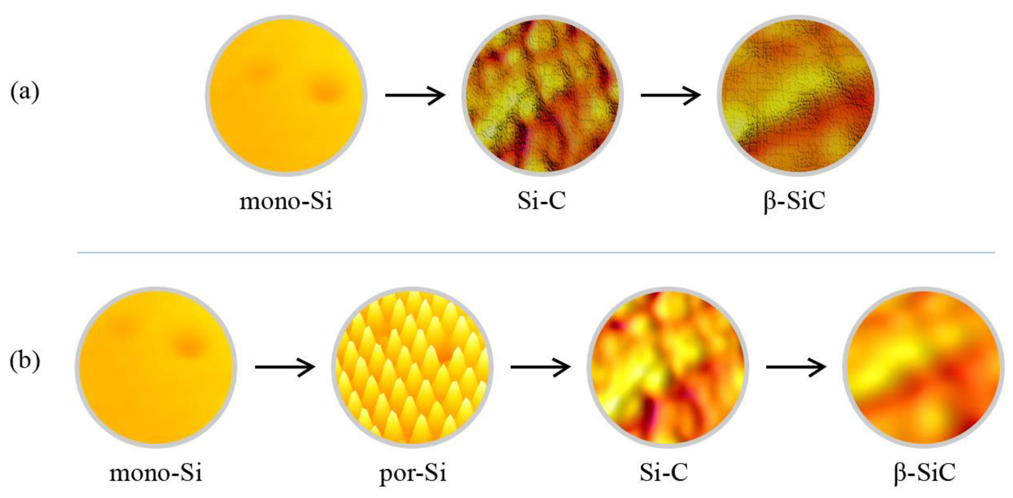
A promising approach to alleviate these issues involves creating a porous layer on the silicon substrate, before SiC deposition. As depicted in Figure 9b, this porous layer can serve as a mechanical buffer, effectively mitigating the excessive elastic pressures that typically arise due to lattice mismatches. The porous architecture essentially functions as a “soft” substrate, facilitating more harmonious integration of SiC with the underlying silicon. Figure 10 represents the SiC film growth on mono-Si (Figure 10a) and por-Si (Figure 10b) substrates. In Figure 10a, the progression from pure mono-Si to a rougher β-SiC film signifies strain due to lattice mismatches. Conversely, in Figure 10b, the por-Si begins with a structured porous surface, and as SiC deposition occurs, it shows a smoother β-SiC film, underscoring the stress-buffering capacity of the porous architecture. This improved consistency in Figure 10b illustrates enhanced film–substrate adhesion and provides empirical support to the viability of the por-Si approach in addressing lattice mismatch challenges.
The lattice mismatch between SiC and Si serves as a fundamental bottleneck in achieving high-quality epitaxial films. However, incorporating a porous buffer layer presents a feasible solution to this problem, as it allows for better stress distribution and enhanced adhesion, ultimately forming superior-quality SiC films.
In conventional thermal methods for forming silicon carbide (SiC), carbon atoms are chemically bonded to silicon atoms by forming Si-C covalent bonds [60,61]. However, a challenge arises when considering the surface properties of monocrystalline silicon (mono-Si), which inherently possesses a smooth topology. Due to the natural occurrence of auto-passivation facilitated by silicon dioxide, monocrystalline silicon surfaces tend to have minimal atoms with dangling or broken bonds [62]. Consequently, this surface morphology impinges upon the efficacy of most traditional techniques for the epitaxial growth of SiC films on mono-Si substrates.
The SiC films grown on such smooth mono-Si substrates are often fraught with many imperfections, both on the surface and within the bulk material. These defects manifest in various forms, including dislocations, stacking faults, and film cracking, as illustrated in Figure 10a. The cracks compromise the mechanical and electronic properties of the material, significantly limiting its application potential.
Contrastingly, when pre-formed on the mono-Si surface, a porous silicon (por-Si) layer offers a more amenable substrate for SiC film growth. The surface of porous silicon is characterized by a rough, textured morphology, depicted in Figure 10b. This textural variation in por-Si is crucial: it engenders micro-protrusions or elevated zones interspersed between the pores. These micro-protrusions act as localized sources of silicon atoms, which can readily bond with incoming carbon atoms during SiC film formation.
The intricate porous architecture thus plays a dual role; first, it provides a multitude of nucleation sites that better facilitate the formation of Si-C bonds, and second, it introduces a level of surface roughness that enhances the mechanical interlocking between the SiC film and the underlying silicon substrate. The result is the formation of a high-quality crystalline β-SiC film, which benefits from reduced defects and superior bond strength.
It is imperative to highlight that the properties and applications of porous silicon as a substrate have been the subject of extensive academic investigations [63,64,65]. These studies underscore the porous structure’s instrumental role in mitigating challenges associated with SiC film growth on monocrystalline silicon, thereby contributing to improved SiC/mono-Si heterostructures.
In summary, while the surface characteristics of monocrystalline silicon have traditionally posed limitations on the growth of defect-free SiC films, introducing a porous silicon layer offers an effective countermeasure. This adaptability can pave the way for developing high-quality SiC films, an area of ongoing research and technological importance.
Many mechanisms have been elucidated in film formation on semiconductor substrates to govern the deposited films’ growth kinetics and morphological evolution. Among these, the paradigms established by Frank–van der Merwe [66,67], Volmer–Weber [68,69], and the Stranski–Krastanov mechanism [70,71] stand out as seminal frameworks.
In the context of the Frank–van der Merwe mechanism, also known as layer-by-layer growth, we observe a unique phenomenon primarily in systems where the film’s and substrate’s crystalline lattice parameters exhibit minimal discrepancy [72,73]. This leads to the formation of what is colloquially termed a “wetting layer,” characterized by the sequential deposition of monatomic layers on the substrate. This mechanism is typically operative when the thermodynamic factors favor minimizing surface and interfacial energies.
Conversely, the Volmer–Weber mechanism is observed in instances with pronounced lattice mismatch between the substrate and the film. Such discrepancies promote the growth of isolated islands on the substrate, negating the formation of an initial wetting layer. The Volmer–Weber mode is driven by the system’s need to minimize the strain energy, which leads to a preferential aggregation of atoms into islands rather than a uniform film.
Situated as an intermediate regime between these two is the Stranski–Krastanov mechanism. In this model, the early stages of the film growth process resemble the Frank–van der Merwe mechanism, characterized by establishing an initial wetting layer [74]. However, owing to a slight lattice mismatch, elastic deformations begin to manifest. These deformations induce compressive stresses in the film, ultimately resulting in the nucleation and growth of three-dimensional, rounded islands atop the wetting layer.
Turning our attention to the growth of silicon carbide (SiC) on silicon (Si) substrates, it becomes evident that the porous silicon (por-Si) layer significantly eases the challenges associated with lattice mismatch, as depicted in Figure 9b. Our findings point to the applicability of the Stranski–Krastanov mechanism in this particular heterostructure. This observation substantiates the role of por-Si as a buffer layer, serving as an effective stress-relief intermediary that accommodates the lattice discrepancies between SiC and Si.
Hence, we have presented a facile yet robust methodology for SiC film growth that deftly addresses the perennial technological constraints of lattice mismatch and the compromised crystalline quality of SiC films. Introducing a por-Si buffer layer acts as a catalyst in optimizing the epitaxial growth process of SiC on silicon substrates. The buffer layer’s role is pivotal, warranting further exploration for future refinements in the growth methodology. Subsequent research endeavors may be directed towards achieving complete carbide formation in SiC/Si structures and the potential for developing graphene layers on the surface of these heterostructures.
Through this multi-faceted analysis, we aim to contribute to the empirical knowledge pool of SiC film growth and broader efforts aimed at technological advancements in semiconductor applications.
5. Conclusions
The current study meticulously elaborates on an enhanced methodology for synthesizing β-SiC films on silicon substrates by judiciously integrating porous silicon (por-Si) as an intermediary buffer layer. Incorporating this buffer layer culminates in augmented adhesion between the SiC film and the mono-Si substrate. The resultant layered material thus manifests as a hybrid heterostructure of β-SiC/por-Si/mono-Si, with implications for advancing the state of the art in semiconductor technologies.
Examinations of the surface morphology via advanced imaging techniques revealed that the synthesized SiC film predominantly consists of island agglomerates with diametric dimensions ranging from 2 to 6 μm. Further intricate features, such as minuscule pores with sizes varying between 70 and 80 nm, were discerned on the islands’ surfaces. Such topological attributes point to an intricate interface interaction and might have ramifications on the mechanical and electronic properties of the resulting heterostructure.
The X-ray Diffraction (XRD) analysis of the synthesized β-SiC/por-Si/mono-Si heterostructure exhibited three distinct peaks at angular positions (2θ) of 28.5°, 35.6°, and 60.1°. These peaks unequivocally correspond to the crystallographic orientations (hkl) of (111) and (220) for silicon (Si) and silicon carbide (SiC) in their cubic symmetry, respectively. This indicates the formation of high-quality crystalline structures. When juxtaposed with the standard peak positions for crystalline silicon, a noticeable shift toward lower angles was observed, particularly in the peak at 2θ = 35.6°. This shift, which represents a deviation from the typical diffraction patterns of bulk silicon, is indicative of quantum size effects. Such effects are consistent with the presence of nanometer-sized objects, as confirmed by Scanning Electron Microscopy (SEM) analyses.
Furthermore, the intensity and uniqueness of the peak at an angular position of 2θ = 35.6°, which aligns with the characteristics of β-SiC in a zinc-blende-type lattice, emphasize the impeccable crystallinity of the SiC layers. The absence of other intense peaks serves as further evidence for this claim, suggesting that the resultant heterostructure retains high structural integrity.
The prospects emerging from our research are expansive. The SiC/por-Si/mono-Si heterostructure promises to revolutionize next-generation electronic devices, given the superior electron mobility and thermal resilience of SiC. In optoelectronics, the heterostructure’s unique electronic and optical attributes could spearhead the development of advanced devices such as photodetectors and light-emitting diodes. Furthermore, the chemical robustness of SiC offers avenues for its adoption in advanced sensing technologies, especially in challenging environments. The juxtaposition of SiC’s admirable thermal conductivity with por-Si’s insulating characteristics paves the path for innovative thermal management solutions for electronic apparatuses. Additionally, the observed quantum size effects signal potential applicability in the burgeoning arena of quantum computing, wherein meticulous control over nanoscale entities is vital.
It is crucial to acknowledge that, while our methodology offers a substantial improvement in overcoming lattice mismatch and adhesion issues that plague the conventional SiC film synthesis on silicon substrates, further research endeavors are requisite. These could include optimizing porosity levels in the buffer layer, a comprehensive assessment of mechanical properties under variable thermal and electrical conditions, and investigating the potential utility of this heterostructure in electronic and optoelectronic applications.
Conclusively, the present study augments the existing body of knowledge by elucidating an efficient, scalable technique for synthesizing high-quality β-SiC films on silicon substrates. The findings portend significant technological benefits and set the stage for subsequent research to refine and expand the application scope of SiC/por-Si/mono-Si heterostructures.
Author Contributions
Conceptualization, Y.S.; methodology, Y.S., S.K. and I.B.; software, Y.S. and S.K.; validation, Y.S., A.L.K., M.V.Z. and A.I.P.; formal analysis, S.K. and I.B.; investigation, Y.S., S.K. and I.B.; resources, Y.S. and A.I.P.; data curation, Y.S., S.K. and A.I.P.; writing—original draft preparation, Y.S., S.K. and A.I.P.; writing—review and editing, Y.S., A.L.K., M.V.Z. and A.I.P.; visualization, Y.S., S.K., A.L.K. and M.V.Z.; supervision, Y.S. and A.I.P.; project administration, Y.S. and A.I.P.; funding acquisition, Y.S. and A.I.P. All authors have read and agreed to the published version of the manuscript.
Funding
The study was supported by the Ministry of Education and Science of Ukraine via Project No. 0122U000129 “The search for optimal conditions for nanostructure synthesis on the surface of A3B5, A2B6 semiconductors and silicon for photonics and solar energy”, Project No. 0121U10942 “Theoretical and methodological bases of system fundamentalization of the future nanomaterials experts training for productive professional activity”, and Project No. 0123U100110 “System of remote and mixed specialized training of future nanoengineers for the development of new dual-purpose nanomaterials”. In addition, the research of A.I.P. and Y.S. was partly supported by COST Action CA20129 “Multiscale irradiation and chemistry driven processes and related technologies” (MultiChem). Y.S. was partly supported by COST Action CA20126—Network for research, innovation, and product development on porous semiconductors and oxides (NETPORE). A.I.P., thanks to the Institute of Solid State Physics, University of Latvia, ISSP UL as the Center of Excellence, is supported through the Framework Program for European Universities, Union Horizon 2020, H2020-WIDESPREAD-01–2016–2017-TeamingPhase2, under Grant Agreement No. 739508, CAMART2 project.
Institutional Review Board Statement
Not applicable.
Informed Consent Statement
Not applicable.
Data Availability Statement
Data is contained within the article.
Conflicts of Interest
The authors declare no conflict of interest.
References
- Chen, D.; Vaqueiro Contreras, M.; Ciesla, A.; Hamer, P.; Hallam, B.; Abbott, M.; Chan, C. Progress in the understanding of light-and elevated temperature-induced degradation in silicon solar cells: A review. Prog. Photovolt. Res. Appl. 2021, 29, 1180–1201. [Google Scholar] [CrossRef]
- Richter, A.; Müller, R.; Benick, J.; Feldmann, F.; Steinhauser, B.; Reichel, C.; Glunz, S.W. Design rules for high-efficiency both-sides-contacted silicon solar cells with balanced charge carrier transport and recombination losses. Nat. Energy 2021, 6, 429–438. [Google Scholar] [CrossRef]
- Andreani, L.C.; Bozzola, A.; Kowalczewski, P.; Liscidini, M.; Redorici, L. Silicon solar cells: Toward the efficiency limits. Adv. Phys. X 2019, 4, 1548305. [Google Scholar] [CrossRef]
- Fell, A.; McIntosh, K.R.; Altermatt, P.P.; Janssen, G.J.; Stangl, R.; Ho-Baillie, A.; Abbott, M.D. Input parameters for the simulation of silicon solar cells in 2014. IEEE J. Photovolt. 2015, 5, 1250–1263. [Google Scholar] [CrossRef]
- Bosio, A.; Pasini, S.; Romeo, N. The History of Photovoltaics with Emphasis on CdTe Solar Cells and Modules. Coatings 2020, 10, 344. [Google Scholar] [CrossRef]
- Çetinkaya, Ç.; Çokduygulular, E.; Kınacı, B.; Güzelçimen, F.; Özen, Y.; Sönmez, N.A.; Özçelik, S. Highly improved light harvesting and photovoltaic performance in CdTe solar cell with functional designed 1D-photonic crystal via light management engineering. Sci. Rep. 2022, 12, 11245. [Google Scholar] [CrossRef]
- Suchikova, Y.; Kovachov, S.; Bohdanov, I. Formation of oxide crystallites on the porous GaAs surface by electrochemical deposition. Nanomater. Nanotechnol. 2022, 12. [Google Scholar] [CrossRef]
- Oshima, R.; Ogura, A.; Shoji, Y.; Makita, K.; Ubukata, A.; Koseki, S.; Imaizumi, M.; Sugaya, T. Ultra-High-Speed Growth of GaAs Solar Cells by Triple-Chamber Hydride Vapor Phase Epitaxy. Crystals 2023, 13, 370. [Google Scholar] [CrossRef]
- Suchikova, Y. Provision of environmental safety through the use of porous semiconductors for solar energy sector. East.-Eur. J. Enterp. Technol. 2016, 6, 26–33. [Google Scholar] [CrossRef]
- Yana, S. Porous indium phosphide: Preparation and properties. In Handbook of Nanoelectrochemistry: Electrochemical Synthesis Methods, Properties, and Characterization Techniques, 1st ed.; Springer: Cham, Switzerland, 2015; pp. 283–306. [Google Scholar] [CrossRef]
- Suchikova, Y.; Kovachov, S.; Bohdanov, I.; Moskina, A.; Popov, A. Characterization of CdxTeyOz/CdS/ZnO Hetero-structures Synthesized by the SILAR Method. Coatings 2023, 13, 639. [Google Scholar] [CrossRef]
- Suchikova, Y.; Kovachov, S.; Bohdanov, I.; Karipbaev, Z.T.; Pankratov, V.; Popov, A.I. Study of the structural and morphological characteristics of the CdxTeyOz nanocomposite obtained on the surface of the CdS/ZnO heterostructure by the SILAR method. Appl. Phys. A 2023, 129, 499. [Google Scholar] [CrossRef]
- Shoji, Y.; Tamaki, R.; Okada, Y. Temperature Dependence of Carrier Extraction Processes in GaSb/AlGaAs Quantum Nanostructure Intermediate-Band Solar Cells. Nanomaterials 2021, 11, 344. [Google Scholar] [CrossRef] [PubMed]
- Suchikova, Y.; Kovachov, S.; Bohdanov, I.; Abdikadirova, A.A.; Kenzhina, I.; Popov, A.I. Electrochemical Growth and Structural Study of the AlxGa1−xAs Nanowhisker Layer on the GaAs Surface. J. Manuf. Mater. Process. 2023, 7, 153. [Google Scholar] [CrossRef]
- Sergeyev, D.; Zhanturina, N.; Aizharikov, A.; Popov, A.I. Influence of “Productive” Impurities (Cd, Na, O) on the Properties of the CuZnSnS Absorber of Model Solar Cells. Latv. J. Phys. Tech. Sci. 2021, 58, 13–23. [Google Scholar] [CrossRef]
- Nugroho, H.S.; Refantero, G.; Septiani, N.L.W.; Iqbal, M.; Marno, S.; Abdullah, H.; Prima, E.C.; Nugraha; Yuliarto, B. A progress review on the modification of CZTS(e)-based thin-film solar cells. J. Ind. Eng. Chem. 2022, 105, 83–110. [Google Scholar] [CrossRef]
- Krotkus, A.; Nevinskas, I.; Norkus, R. Semiconductor Characterization by Terahertz Excitation Spectroscopy. Materials 2023, 16, 2859. [Google Scholar] [CrossRef]
- Obaid, W.O.; Hashim, A. Synthesis and Augmented Optical Properties of PC/SiC/TaC Hybrid Nanostructures for Potential and Photonics Fields. Silicon 2022, 14, 11199–11207. [Google Scholar] [CrossRef]
- Vambol, S.O.; Bohdanov, I.T.; Vambol, V.V.; Nestorenko, T.P.; Onyschenko, S.V. Formation of filamentary structures of oxide on the surface of monocrystalline gallium arsenide. J. Nano-Electron. Phys. 2017, 9, 06016. [Google Scholar] [CrossRef]
- Ahmed, H.; Hashim, A. Tuning the spectroscopic and electronic characteristics of ZnS/SiC nanostructures doped organic material for optical and nanoelectronics fields. Silicon 2023, 15, 2339–2348. [Google Scholar] [CrossRef]
- Anjum, S.; Gonzalez, P.E.; Atwater, H.A. Planar and Nanowire InP Thin Solar Cells for Ultralight Space Power Applications. In Proceedings of the 2022 IEEE 49th Photovoltaics Specialists Conference (PVSC), Philadelphia, PA, USA, 5–10 June 2022; pp. 1083–1085. [Google Scholar] [CrossRef]
- Yan, G.; Wang, J.L.; Liu, J.; Liu, Y.Y.; Wu, R.; Wang, R. Electroluminescence analysis of VOC degradation of individual subcell in GaInP/GaAs/Ge space solar cells irradiated by 1.0 MeV electrons. J. Lumin. 2020, 219, 116905. [Google Scholar] [CrossRef]
- Köhler, M.; Pomaska, M.; Procel, P.; Santbergen, R.; Zamchiy, A.; Macco, B.; Lambertz, A.; Duan, W.; Cao, P.; Klingebiel, B.; et al. A silicon carbide-based highly transparent passivating contact for crystalline silicon solar cells approaching efficiencies of 24%. Nat. Energy 2021, 6, 529–537. [Google Scholar] [CrossRef]
- Zhou, L.; Xu, Y.; Tan, S.; Liu, M.; Wan, Y. Simulation of Amorphous Silicon Carbide Photonic Crystal Absorption Layer for Solar Cells. Crystals 2022, 12, 665. [Google Scholar] [CrossRef]
- Hsu, C.-H.; Zhang, X.-Y.; Zhao, M.J.; Lin, H.-J.; Zhu, W.-Z.; Lien, S.-Y. Silicon Heterojunction Solar Cells with p-Type Silicon Carbon Window Layer. Crystals 2019, 9, 402. [Google Scholar] [CrossRef]
- Merkininkaite, G.; Gailevicius, D.; Staisiunas, L.; Ezerskyte, E.; Vargalis, R.; Malinauskas, M.; Sakirzanovas, S. Additive Manufacturing of SiOC, SiC, and Si3N4 Ceramic 3D Microstructures. Adv. Eng. Mater. 2023, 25, 2300639. [Google Scholar] [CrossRef]
- Hashim, A.; Abbas, M.H.; Al-Aaraji NA, H.; Hadi, A. Controlling the morphological, optical and dielectric characteristics of PS/SiC/CeO2 nanostructures for nanoelectronics and optics fields. J. Inorg. Organomet. Polym. Mater. 2023, 33, 1–9. [Google Scholar] [CrossRef]
- Gaibnazarov, B.B.; Imanova, G.; Khozhiev, S.T.; Kosimov, I.O.; Khudaikulov, I.K.; Kuchkanov, S.K.; Bekpulatov, I.R. Changes in the Structure and Properties of Silicon Carbide under Gamma Irradiation. Integr. Ferroelectr. 2023, 237, 208–215. [Google Scholar] [CrossRef]
- Meteab, M.H.; Hashim, A.; Rabee, B.H. Synthesis and tailoring the morphological, optical, electronic and photodegradation characteristics of PS–PC/MnO2–SiC quaternary nanostructures. Opt. Quantum Electron. 2023, 55, 187. [Google Scholar] [CrossRef]
- Kim, V.V.; Konda, S.R.; Yu, W.; Li, W.; Ganeev, R.A. Harmonics Generation in the Laser-Induced Plasmas of Metal and Semiconductor Carbide Nanoparticles. Nanomaterials 2022, 12, 4228. [Google Scholar] [CrossRef]
- Hashim, A.; Abbas, M.H.; Al-Aaraji NA, H.; Hadi, A. Facile fabrication and developing the structural, optical and electrical properties of SiC/Y2O3 nanostructures doped PMMA for optics and potential nanodevices. Silicon 2023, 15, 1283–1290. [Google Scholar] [CrossRef]
- Scalise, E.; Zimbone, M.; Marzegalli, A. Impact of Inversion Domain Boundaries on the Electronic Properties of 3C-SiC. Phys. Status Solidi B 2022, 259, 2200093. [Google Scholar] [CrossRef]
- Kohn, V.G.; Argunova, T.S. Near-Field Phase-Contrast Imaging of Micropores in Silicon Carbide Crystals with Synchrotron Radiation. Phys. Status Solidi B 2022, 259, 2100651. [Google Scholar] [CrossRef]
- Sameera, J.N.; Islam, M.A.; Islam, S.; Hossain, T.; Sobayel, M.; Akhtaruzzaman; Amin, N.; Rashid, M.J. Cubic Silicon Carbide (3C–SiC) as a buffer layer for high efficiency and highly stable CdTe solar cell. Opt. Mater. 2021, 123, 111911. [Google Scholar] [CrossRef]
- Lebedev, A.S.; Suzdal’tsev, A.V.; Anfilogov, V.N.; Farlenkov, A.S.; Porotnikova, N.M.; Vovkotrub, E.G.; Akashev, L.A. Carbothermal Synthesis, Properties, and Structure of Ultrafine SiC Fibers. Inorg. Mater. 2020, 56, 20–27. [Google Scholar] [CrossRef]
- Capan, I. 4H-SiC Schottky Barrier Diodes as Radiation Detectors: A Review. Electronics 2022, 11, 532. [Google Scholar] [CrossRef]
- Li, G.; Xu, M.; Zou, D.; Cui, Y.; Zhong, Y.; Cui, P.; Cheong, K.Y.; Xia, J.; Nie, H.; Li, S.; et al. Fabrication of Ohmic Contact on N-Type SiC by Laser Annealed Process: A Review. Crystals 2023, 13, 1106. [Google Scholar] [CrossRef]
- Tahani, M.; Postek, E.; Motevalizadeh, L.; Sadowski, T. Effect of Vacancy Defect Content on the Interdiffusion of Cubic and Hexagonal SiC/Al Interfaces: A Molecular Dynamics Study. Molecules 2023, 28, 744. [Google Scholar] [CrossRef]
- Chaturvedi, M.; Haasmann, D.; Moghadam, H.A.; Dimitrijev, S. Electrically Active Defects in SiC Power MOSFETs. Energies 2023, 16, 1771. [Google Scholar] [CrossRef]
- Meli, A.; Muoio, A.; Reitano, R.; Sangregorio, E.; Calcagno, L.; Trotta, A.; Parisi, M.; Meda, L.; La Via, F. Effect of the Oxidation Process on Carrier Lifetime and on SF Defects of 4H SiC Thick Epilayer for Detection Applications. Micromachines 2022, 13, 1042. [Google Scholar] [CrossRef]
- Mukesh, N.; Márkus, B.G.; Jegenyes, N.; Bortel, G.; Bezerra, S.M.; Simon, F.; Beke, D.; Gali, A. Formation of Paramagnetic Defects in the Synthesis of Silicon Carbide. Micromachines 2023, 14, 1517. [Google Scholar] [CrossRef]
- Jorudas, J.; Šimukovič, A.; Dub, M.; Sakowicz, M.; Prystawko, P.; Indrišiūnas, S.; Kovalevskij, V.; Rumyantsev, S.; Knap, W.; Kašalynas, I. AlGaN/GaN on SiC Devices without a GaN Buffer Layer: Electrical and Noise Characteristics. Micromachines 2020, 11, 1131. [Google Scholar] [CrossRef]
- Adamov, R.B.; Pashnev, D.; Shalygin, V.A.; Moldavskaya, M.D.; Vinnichenko, M.Y.; Janonis, V.; Jorudas, J.; Tumėnas, S.; Prystawko, P.; Krysko, M.; et al. Optical Performance of Two Dimensional Electron Gas and GaN:C Buffer Layers in AlGaN/AlN/GaN Heterostructures on SiC Substrate. Appl. Sci. 2021, 11, 6053. [Google Scholar] [CrossRef]
- Triani, R.M.; Neto, J.B.T.D.R.; De Oliveira, P.G.B.; Rêgo, G.C.; Neto, A.L.; Casteletti, L.C. In-Situ Production of Metal Matrix Composites Layers by TIG Surface Alloying to Improve Wear Resistance of Ductile Cast Iron Using a Buffer-Layer and Post Weld Heat Treatment. Coatings 2023, 13, 1137. [Google Scholar] [CrossRef]
- Lenshin, A.; Seredin, P.; Goloshchapov, D.; Radam, A.O.; Mizerov, A. MicroRaman Study of Nanostructured Ultra-Thin AlGaN/GaN Thin Films Grown on Hybrid Compliant SiC/Por-Si Substrates. Coatings 2022, 12, 626. [Google Scholar] [CrossRef]
- Amador-Mendez, N.; Mathieu-Pennober, T.; Vézian, S.; Chauvat, M.P.; Morales, M.; Ruterana, P.; Babichev, A.; Bayle, F.; Julien, F.H.; Bouchoule, S.; et al. Porous nitride light-emitting diodes. ACS Photonics 2022, 9, 1256–1263. [Google Scholar] [CrossRef]
- Faltakh, H.; Bourguiga, R.; Ben Rabha, M.; Bessais, B. Simulation and Optimization of the Performance of Multicrystalline Silicon Solar Cell Using Porous Silicon Antireflection Coating Layer. Superlattices Microstruct. 2014, 72, 283–295. [Google Scholar] [CrossRef]
- Ben Rabha, M.; Mohamed, S.B.; Dimassi, W.; Gaidi, M.; Ezzaouia, H.; Bessais, B. Reduction of Absorption Loss in Multicrystalline Silicon via Combination of Mechanical Grooving and Porous Silicon. Phys. Status Solidi C 2011, 8, 883–886. [Google Scholar] [CrossRef]
- Nafie, N.; Lachiheb, M.A.; Rabha, M.B.; Dimassi, W.; Bouaïcha, M. Effect of the Doping Concentration on the Properties of Silicon Nanowires. Phys. E Low-Dimens. Syst. Nanostruc. 2014, 56, 427–430. [Google Scholar] [CrossRef]
- Lo Nigro, R.; Fiorenza, P.; Greco, G.; Schilirò, E.; Roccaforte, F. Structural and Insulating Behaviour of High-Permittivity Binary Oxide Thin Films for Silicon Carbide and Gallium Nitride Electronic Devices. Materials 2022, 15, 830. [Google Scholar] [CrossRef]
- Fiorenza, P.; Giannazzo, F.; Roccaforte, F. Characterization of SiO2/4H-SiC Interfaces in 4H-SiC MOSFETs: A Review. Energies 2019, 12, 2310. [Google Scholar] [CrossRef]
- Zhu, S.; Liu, T.; Fan, J.; Maddi, H.L.R.; White, M.H.; Agarwal, A.K. Effects of JFET Region Design and Gate Oxide Thickness on the Static and Dynamic Performance of 650 V SiC Planar Power MOSFETs. Materials 2022, 15, 5995. [Google Scholar] [CrossRef]
- Brzozowski, E.; Kaminski, M.; Taube, A.; Sadowski, O.; Krol, K.; Guziewicz, M. Carrier Trap Density Reduction at SiO2/4H-Silicon Carbide Interface with Annealing Processes in Phosphoryl Chloride and Nitride Oxide Atmospheres. Materials 2023, 16, 4381. [Google Scholar] [CrossRef] [PubMed]
- Sultan, N.M.; Albarody, T.M.B.; Obodo, K.O.; Baharom, M.B. Effect of Mn+2 Doping and Vacancy on the Ferromagnetic Cubic 3C-SiC Structure Using First Principles Calculations. Crystals 2023, 13, 348. [Google Scholar] [CrossRef]
- Kukushkin, S.A.; Osipov, A.V. Anomalous Properties of the Dislocation-Free Interface between Si(111) Substrate and 3C-SiC(111) Epitaxial Layer. Materials 2021, 14, 78. [Google Scholar] [CrossRef] [PubMed]
- Scuderi, V.; Zielinski, M.; La Via, F. Impact of Doping on Cross-Sectional Stress Assessment of 3C-SiC/Si Heteroepitaxy. Materials 2023, 16, 3824. [Google Scholar] [CrossRef] [PubMed]
- Zimbone, M.; Zielinski, M.; Bongiorno, C.; Calabretta, C.; Anzalone, R.; Scalese, S.; Fisicaro, G.; La Magna, A.; Mancarella, F.; La Via, F. 3C-SiC Growth on Inverted Silicon Pyramids Patterned Substrate. Materials 2019, 12, 3407. [Google Scholar] [CrossRef]
- Zhang, R.; Zou, C.; Wei, Z.; Wang, H.; Liu, C. Nano-Phase and SiC–Si Spherical Microstructure in SiC/Al-50Si Composites Solidified under High Pressure. Materials 2023, 16, 4283. [Google Scholar] [CrossRef]
- Suchikova, Y.O.; Kovachov, S.S.; Bardus, I.O.; Lazarenko, A.S.; Bohdanov, I.T. Formation of β-SiC on por-Si/mono-Si Surface According to Stranski—Krastanow Mechanism. Him. Fiz. Tehnol. Poverhni 2022, 13, 447–454. [Google Scholar] [CrossRef]
- Lobanok, M.V.; Mukhammad, A.I.; Gaiduk, P.I. Structural and Optical Properties of SiC/Si Heterostructures Obtained Using Rapid Vacuum-Thermal Carbidization of Silicon. J. Appl. Spectrosc. 2022, 89, 256–260. [Google Scholar] [CrossRef]
- Kulych, V.G.; Fesenko, I.P.; Kovtiukh, M.O.; Tkach, V.M.; Kaidash, O.M.; Kuzmenko, Y.F.; Chasnyk, V.I.; Ivzhenko, V.V. Microstructure and Thermal Conductivity of Reaction-Sintered SiC. J. Superhard Mater. 2023, 45, 158–160. [Google Scholar] [CrossRef]
- Song, Y.; Zhang, G.; Cai, X.; Dou, B.; Wang, Z.; Liu, Y.; Wei, S.H. General Model for Defect Dynamics in Ionizing-Irradiated SiO2-Si Structures. Small 2022, 18, 2107516. [Google Scholar] [CrossRef]
- Bandarenka, H.; Redko, S.; Nenzi, P.; Balucani, M. Optimization of chemical displacement deposition of copper on porous silicon. J. Nanosci. Nanotechnol. 2012, 12, 8725–8731. [Google Scholar] [CrossRef] [PubMed]
- Dolgyi, A.; Bandarenka, H.; Prischepa, S.; Yanushkevich, K.; Nenzi, P.; Balucani, M.; Bondarenko, V. Electrochemical deposition of Ni into mesoporous silicon. ECS Trans. 2012, 41, 111. [Google Scholar] [CrossRef]
- Artsemyeva, K.; Dolgiy, A.; Bandarenka, H.; Panarin, A.; Khodasevich, I.; Terekhov, S.; Bondarenko, V. Fabrication of SERS-active substrates by electrochemical and electroless deposition of metals in macroporous silicon. ECS Trans. 2013, 53, 85. [Google Scholar] [CrossRef]
- Wang, H.; Yao, Z.; Jung, G.S.; Song, Q.; Hempel, M.; Palacios, T.; Kong, J. Frank-van der Merwe Growth in Bilayer Graphene. Matter 2021, 4, 3339–3353. [Google Scholar] [CrossRef]
- Zhai, P.; Kou, S.; Peng, Y.; Shi, Y.; Jiang, H.; Li, G. Change Volmer–Weber to Frank–van der Merwe Growth Model of Epitaxial BiVO4 Film. J. Phys. D Appl. Phys. 2022, 55, 324004. [Google Scholar] [CrossRef]
- Gastellóu, E.; García, R.; Herrera, A.M.; Ramos, A.; García, G.; Hirata, G.A.; Ramírez, Y.D. Optical and Structural Analysis of GaN Microneedle Crystals Obtained via GaAs Substrates Decomposition and their Possible Growth Model Using the Volmer–Weber Mechanism. Phys. Status Solidi B 2023, 260, 2200201. [Google Scholar] [CrossRef]
- Qiu, X.P.; Liu, X.; Jiang, S.M. Growth Mechanism for Zinc Coatings Deposited by Vacuum Thermal Evaporation. J. Iron Steel Res. Int. 2021, 28, 1047–1053. [Google Scholar] [CrossRef]
- Dirko, V.V.; Lozovoy, K.A.; Kokhanenko, A.P.; Kukenov, O.I.; Korotaev, A.G.; Voitsekhovskii, A.V. Peculiarities of the 7 × 7 to 5 × 5 Superstructure Transition during Epitaxial Growth of Germanium on Silicon (111) Surface. Nanomaterials 2023, 13, 231. [Google Scholar] [CrossRef]
- Penha, F.M.; Andrade, F.R.D.; Lanzotti, A.S.; Moreira Junior, P.F.; Zago, G.P.; Seckler, M.M. In Situ Observation of Epitaxial Growth during Evaporative Simultaneous Crystallization from Aqueous Electrolytes in Droplets. Crystals 2021, 11, 1122. [Google Scholar] [CrossRef]
- Sun, X.W.; Huang, H.C.; Kwok, H.S. On the initial growth of indium tin oxide on glass. Appl. Phys. Lett. 1996, 68, 2663–2665. [Google Scholar] [CrossRef]
- Floro, J.A.; Hearne, S.J.; Hunter, J.A.; Seel, S.C.; Thompson, C.V. The dynamic competition between stress generation and relaxation mechanisms during coalescence of Volmer-Weber thin films. J. Appl. Phys. 2001, 89, 4886–4897. [Google Scholar] [CrossRef]
- Pan, L.; Lew, K.-K.; Redwing, J.M.; Dickey, E.C. Stranski-Krastanow growth of germanium on silicon nanowires. Nano Lett. 2005, 5, 1081–1085. [Google Scholar] [CrossRef] [PubMed]
Figure 1.
Schematic diagram of the formation of the Si porous layer.
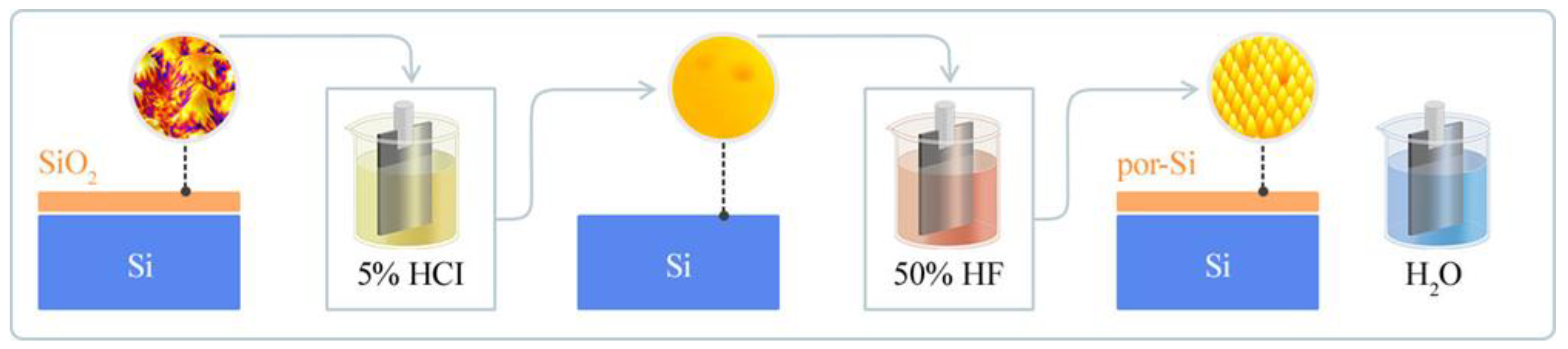
Figure 2.
Schematic diagram of the formation of the heterostructure β-SiC/por-Si/mono-Si.
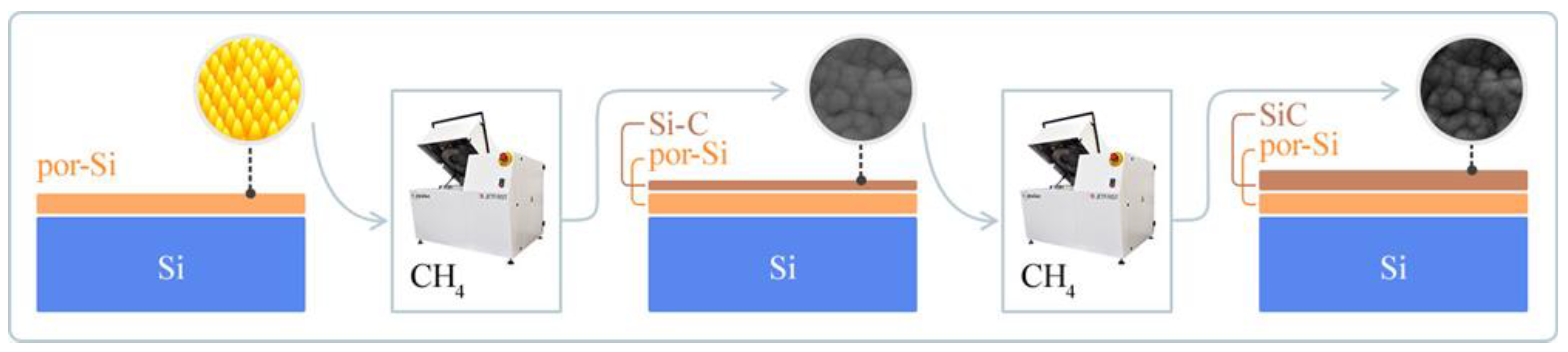
Figure 3.
Surface morphology of the β-SiC/por-Si/mono-Si heterostructure.
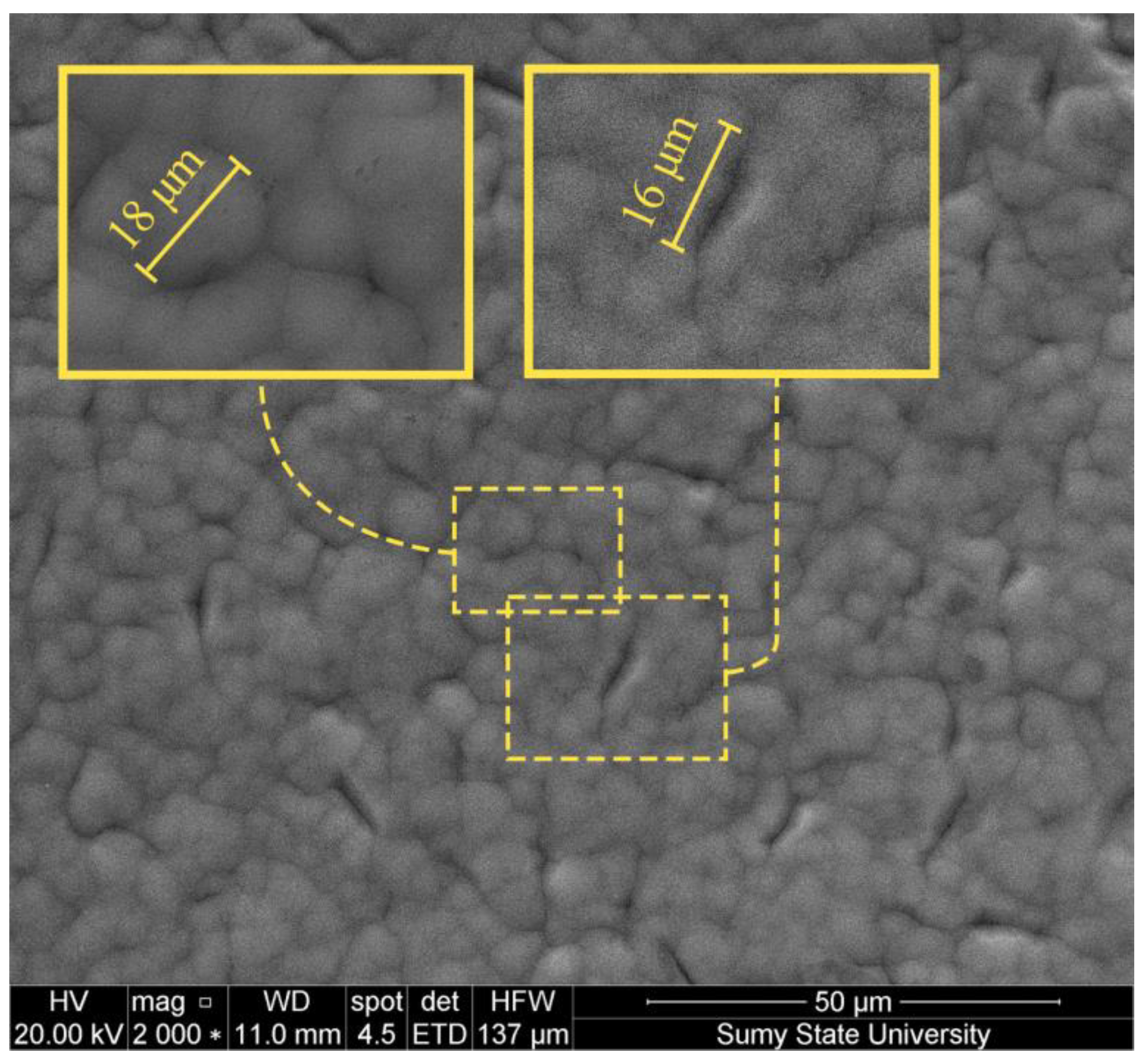
Figure 4.
Diameter distribution diagram of the SiC film islands.
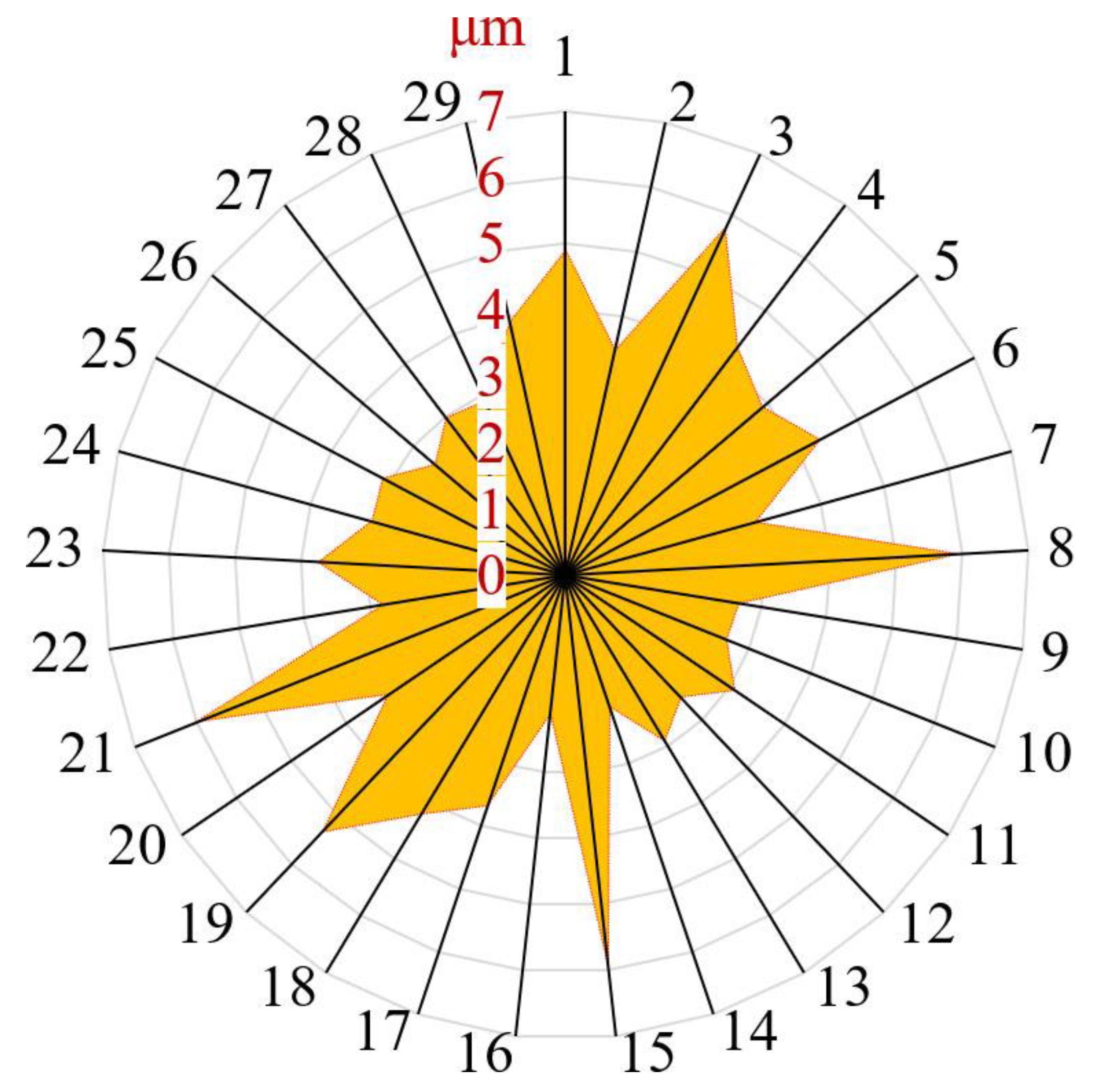
Figure 5.
Cross-section of the β-SiC/por-Si/mono-Si film.
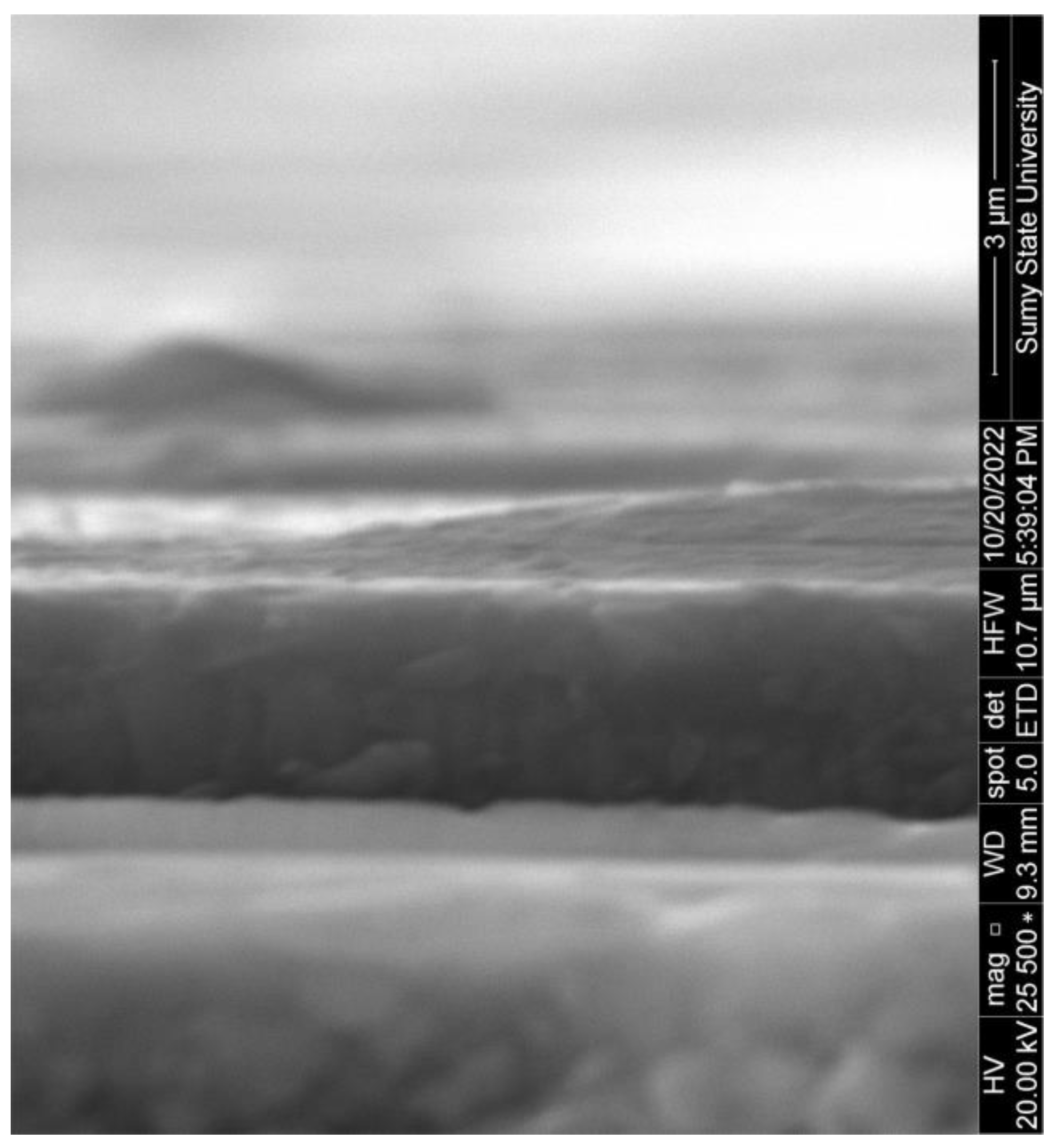
Figure 6.
EDX analysis of the surface of the heterostructure β-SiC/por-Si/mono-Si obtained using mapping technology.
Figure 6.
EDX analysis of the surface of the heterostructure β-SiC/por-Si/mono-Si obtained using mapping technology.
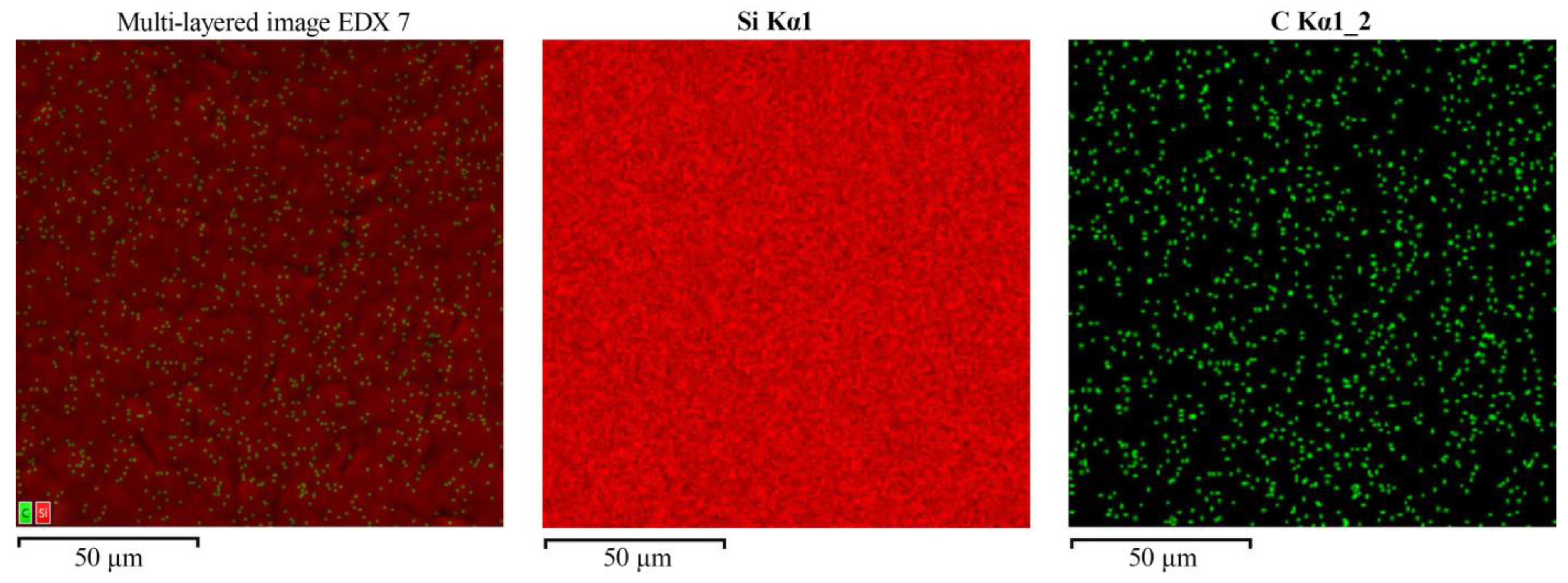
Figure 7.
EDX spectrum of the surface of the β-SiC/por-Si/mono-Si heterostructure; inset shows the percentage composition of elements.
Figure 7.
EDX spectrum of the surface of the β-SiC/por-Si/mono-Si heterostructure; inset shows the percentage composition of elements.
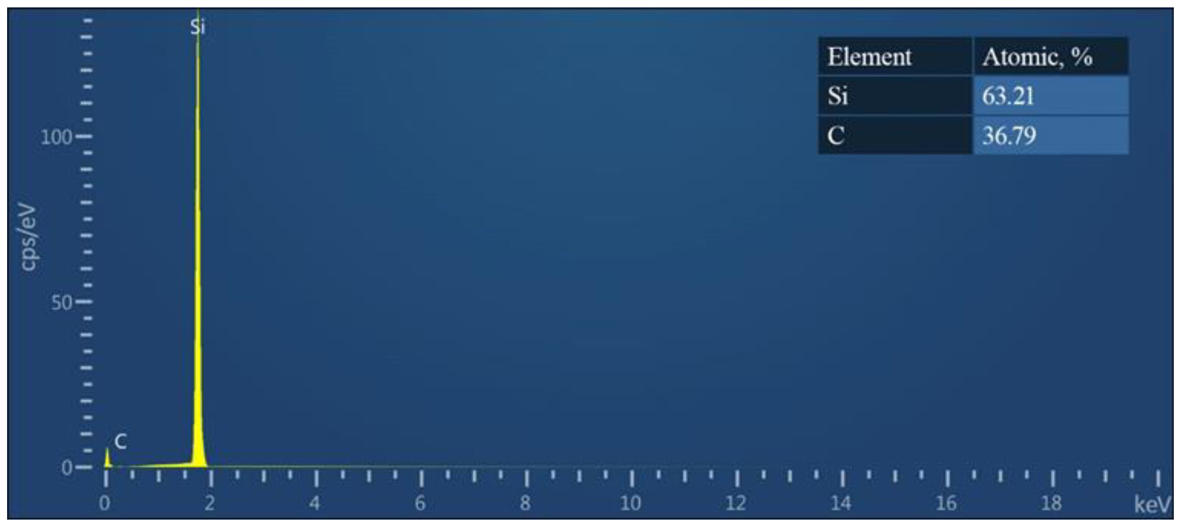
Figure 8.
XRD pattern of β-SiC/por-Si/mono-Si heterostructure.
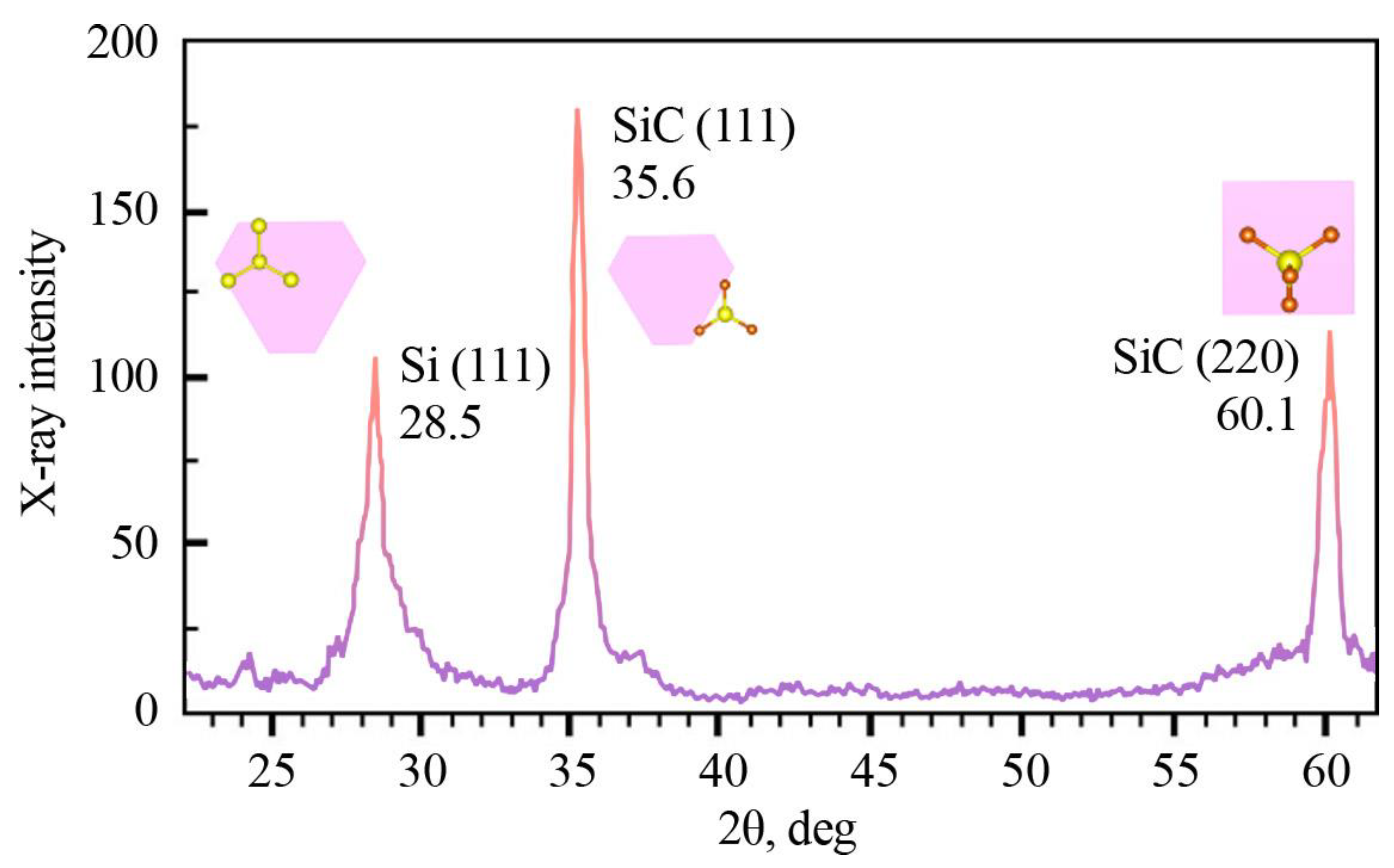
Figure 9.
Schematic representation of the formation of SiC/Si heterostructures (a) and SiC/por-Si/Si (b).
Figure 9.
Schematic representation of the formation of SiC/Si heterostructures (a) and SiC/por-Si/Si (b).
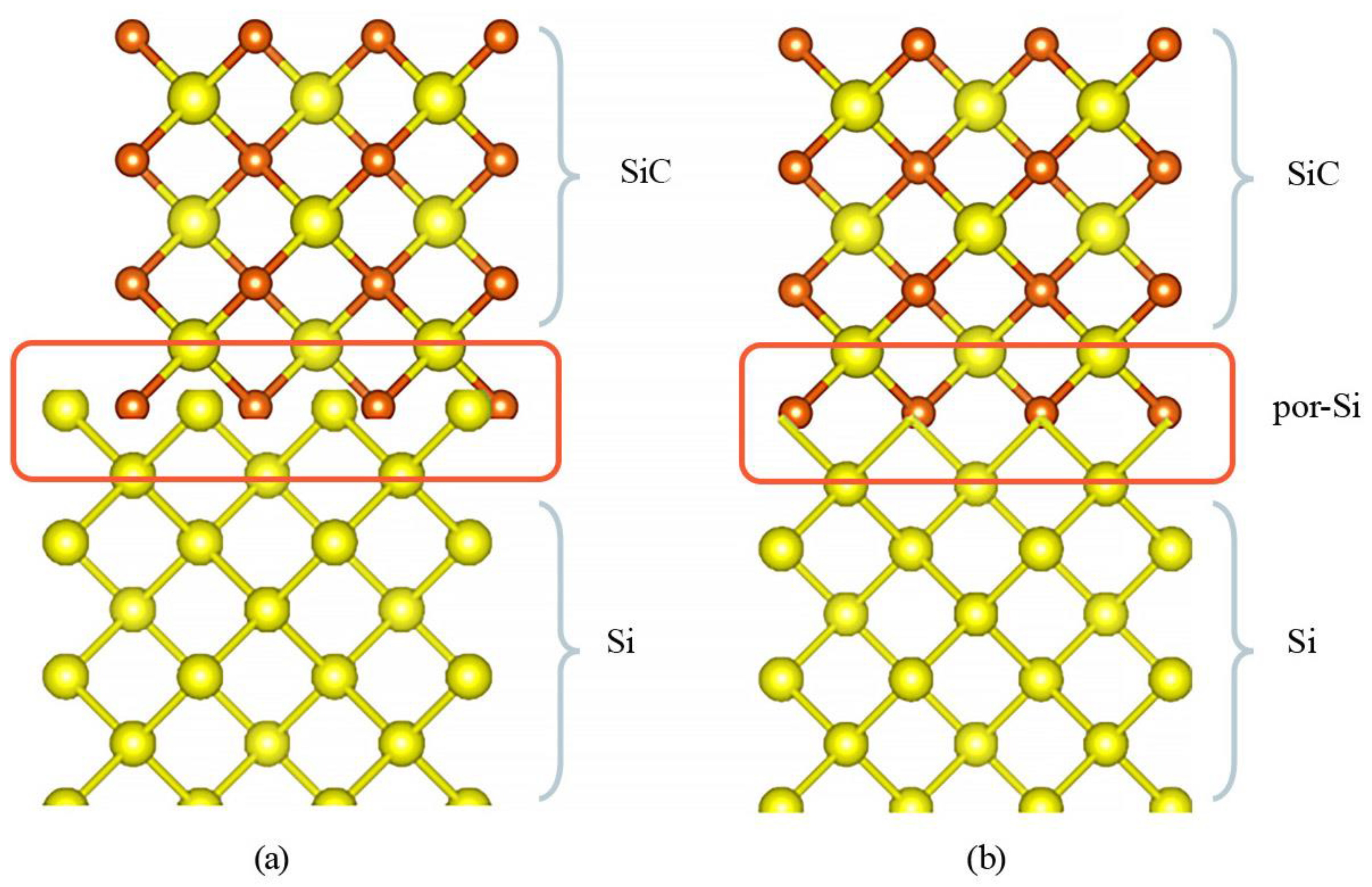
Figure 10.
Simulation of the SiC film growth process on the surface of mono-Si (a) and por-Si (b).

Table 1.
Conditions and sub-stages of Si sample preparation.
| № | Purpose | Electrolyte | Potential, V | Time, min |
|---|---|---|---|---|
| 1.1 | Removal of oxide | 5% HCl | 2 | 3 |
| 1.2 | Formation of a porous layer | 50% HF | 5 | 7 |
| 1.3 | Removal of reaction products from the surface | H2O | 0 | 2 |
Table 2.
Conditions and sub-stages for removing moisture residues from the por-Si surface.
| № | Time, min | Temperature, °C |
|---|---|---|
| 2.1 | 180 | 150 |
| 2.2 | 60 | 300 |
| 2.3 | 60 | 400 |
Table 3.
Parameters for por-Si surface carbonization.
| № | Time, min | Temperature, °C | Pressure in the Reaction Chamber, P, Pa |
|---|---|---|---|
| 3.1 | 1 | 50→900 1 | 1 × 10⁻² |
| 3.2 | 1 | 50→900 | 1 × 10⁻² |
1 The notation (50→900) indicates that the temperature was gradually increased within the specified ranges. The interval between processing batches was 1 min. These short carbonization batches ensure uniform carbon distribution on the surface, which is essential for forming a high-quality thin silicon carbide layer.
Table 4.
Parameters for post-processing the surface of the formed β-SiC/por-Si/mono-Si heterostructure.
Table 4.
Parameters for post-processing the surface of the formed β-SiC/por-Si/mono-Si heterostructure.
| № | Method | Reagent | Time, min | Temperature, °C |
|---|---|---|---|---|
| 4.1 | Chemical etching | 2% HCl | 20 | 20 |
| 4.2 | Thermal annealing | N2 | 90 | 150 |
Table 5.
Crystal structures determined by XRD spectrophotometry.
| № | 2θ, ° | hkl | Crystal | Crystal System |
|---|---|---|---|---|
| 1 | 28.5 | (111) | Si | Cubic |
| 2 | 35.6 | (111) | Si | Cubic |
| 3 | 60.1 | (220) | SiC | Cubic |
Table 6.
Structural parameters of Si and SiC.
| Parameter | Si | SiC |
|---|---|---|
| Crystal system | Cubic | Cubic |
| Space group name | P1 | F-43m |
| Lattice parameters, Å | a = 4.348 | a = 5.6608 |
| Unit-cell volume, 10−6 pm−3 | 82.20 | 181.39 |
Disclaimer/Publisher’s Note: The statements, opinions and data contained in all publications are solely those of the individual author(s) and contributor(s) and not of MDPI and/or the editor(s). MDPI and/or the editor(s) disclaim responsibility for any injury to people or property resulting from any ideas, methods, instructions or products referred to in the content. |
© 2023 by the authors. Licensee MDPI, Basel, Switzerland. This article is an open access article distributed under the terms and conditions of the Creative Commons Attribution (CC BY) license (https://creativecommons.org/licenses/by/4.0/).
Share and Cite
MDPI and ACS Style
Suchikova, Y.; Kovachov, S.; Bohdanov, I.; Kozlovskiy, A.L.; Zdorovets, M.V.; Popov, A.I. Improvement of β-SiC Synthesis Technology on Silicon Substrate. Technologies 2023, 11, 152. https://doi.org/10.3390/technologies11060152
AMA Style
Suchikova Y, Kovachov S, Bohdanov I, Kozlovskiy AL, Zdorovets MV, Popov AI. Improvement of β-SiC Synthesis Technology on Silicon Substrate. Technologies. 2023; 11(6):152. https://doi.org/10.3390/technologies11060152
Chicago/Turabian StyleSuchikova, Yana, Sergii Kovachov, Ihor Bohdanov, Artem L. Kozlovskiy, Maxim V. Zdorovets, and Anatoli I. Popov. 2023. "Improvement of β-SiC Synthesis Technology on Silicon Substrate" Technologies 11, no. 6: 152. https://doi.org/10.3390/technologies11060152
Note that from the first issue of 2016, this journal uses article numbers instead of page numbers. See further details here.