Development of a Transmission Line Model for the Thickness Prediction of Thin Films via the Infrared Interference Method †

 , , and
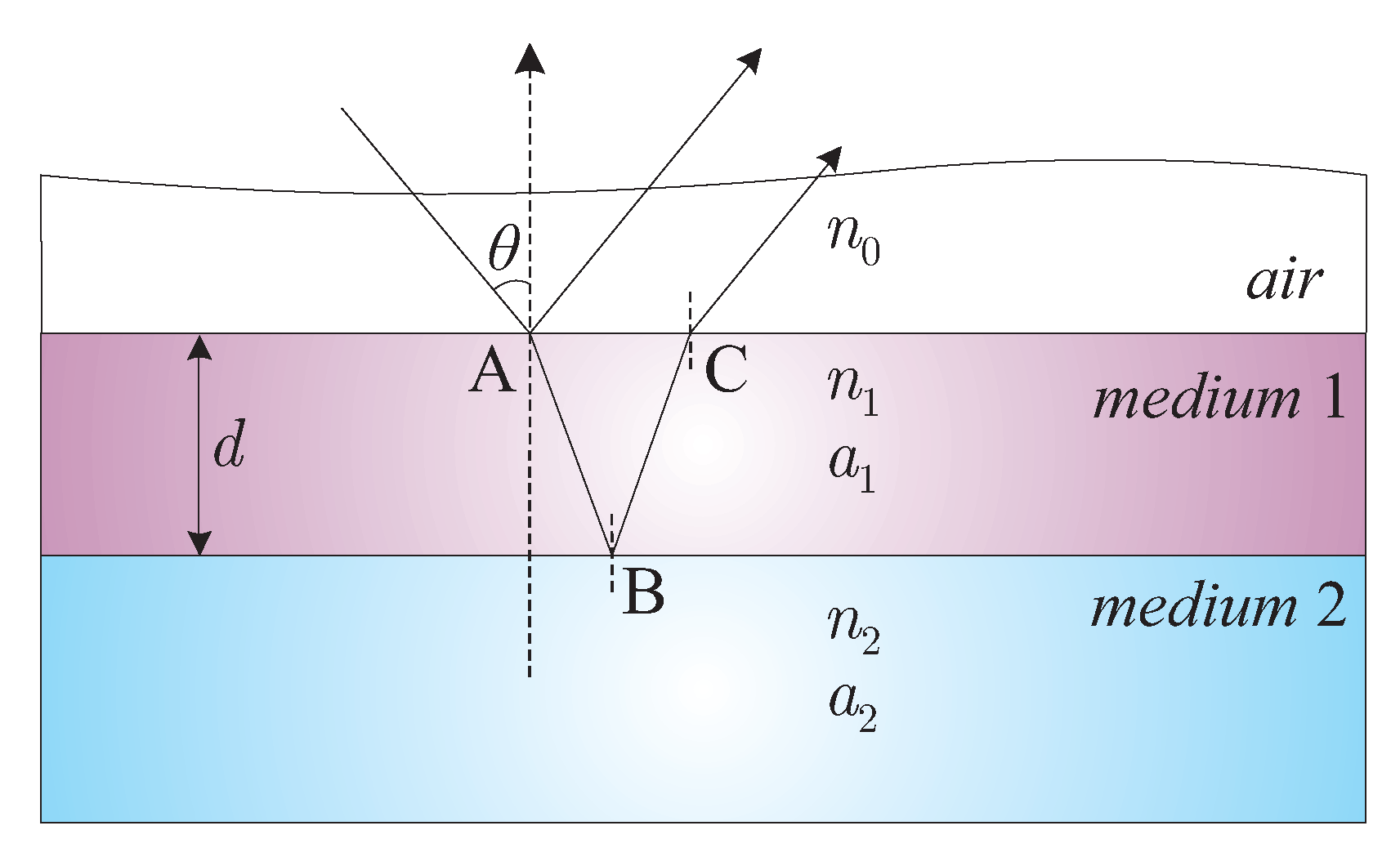
Abstract
:1. Materials and Methods
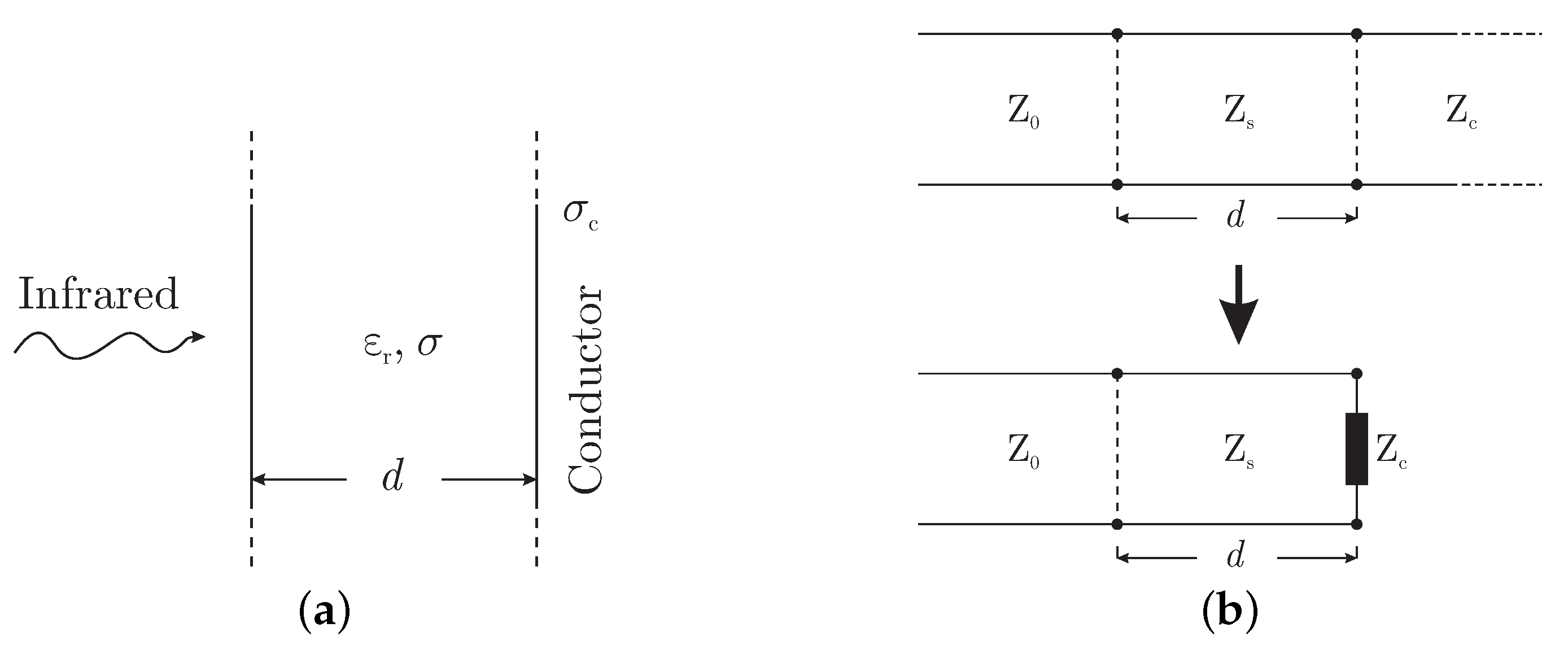
1.1. Main Concept and Theoretical Formulation
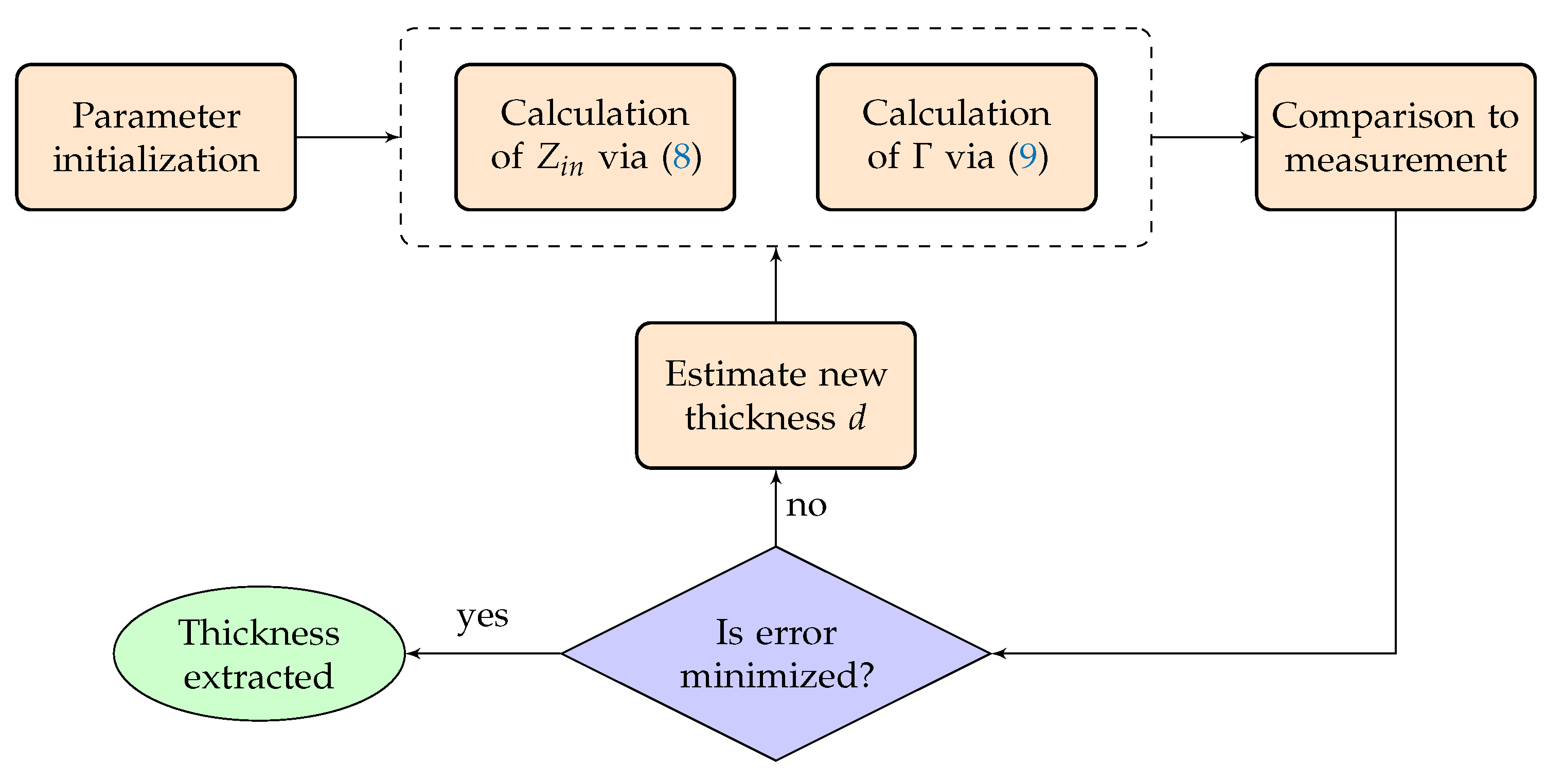
1.2. Design and Analysis of the Proposed Model
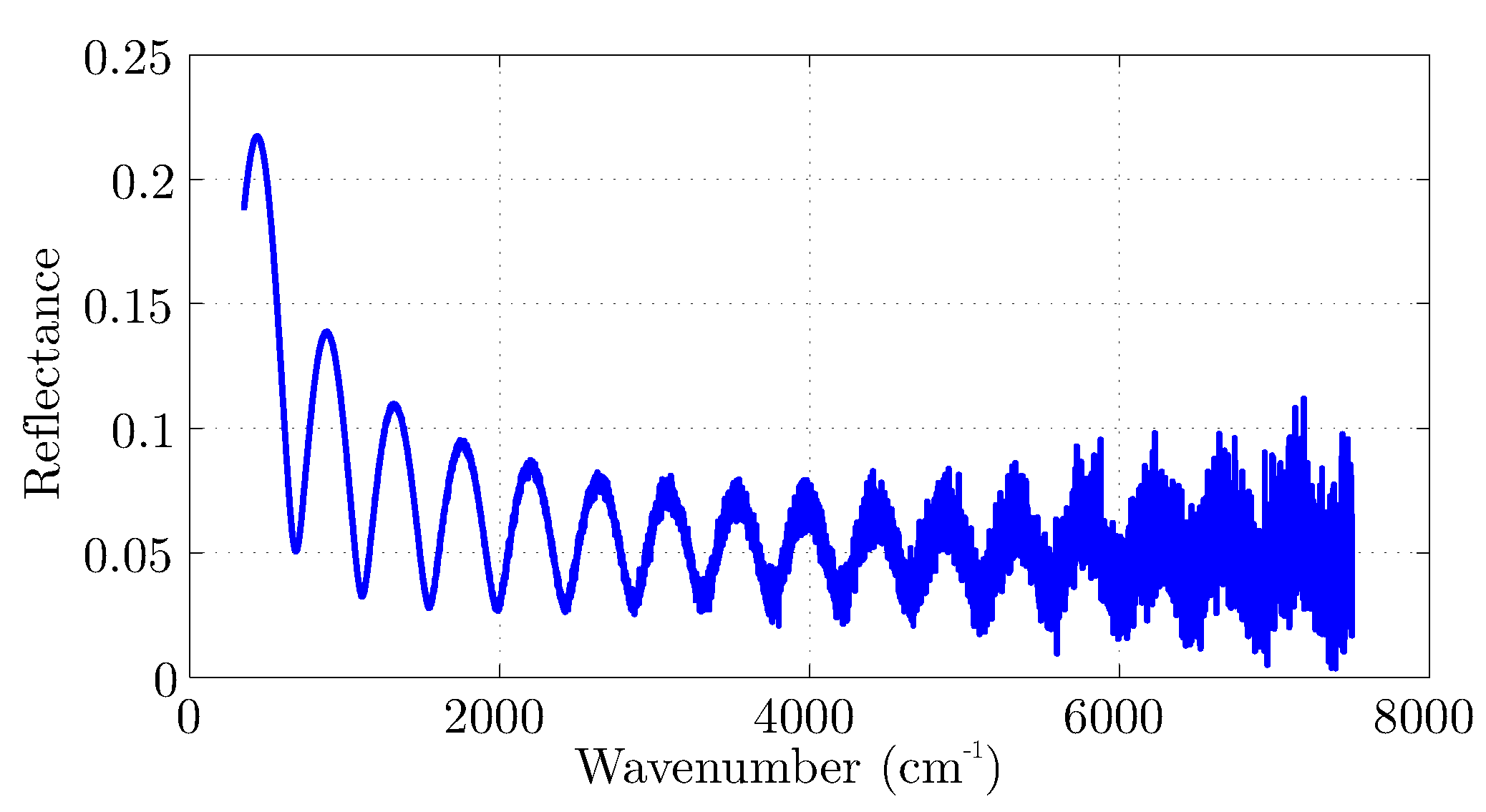
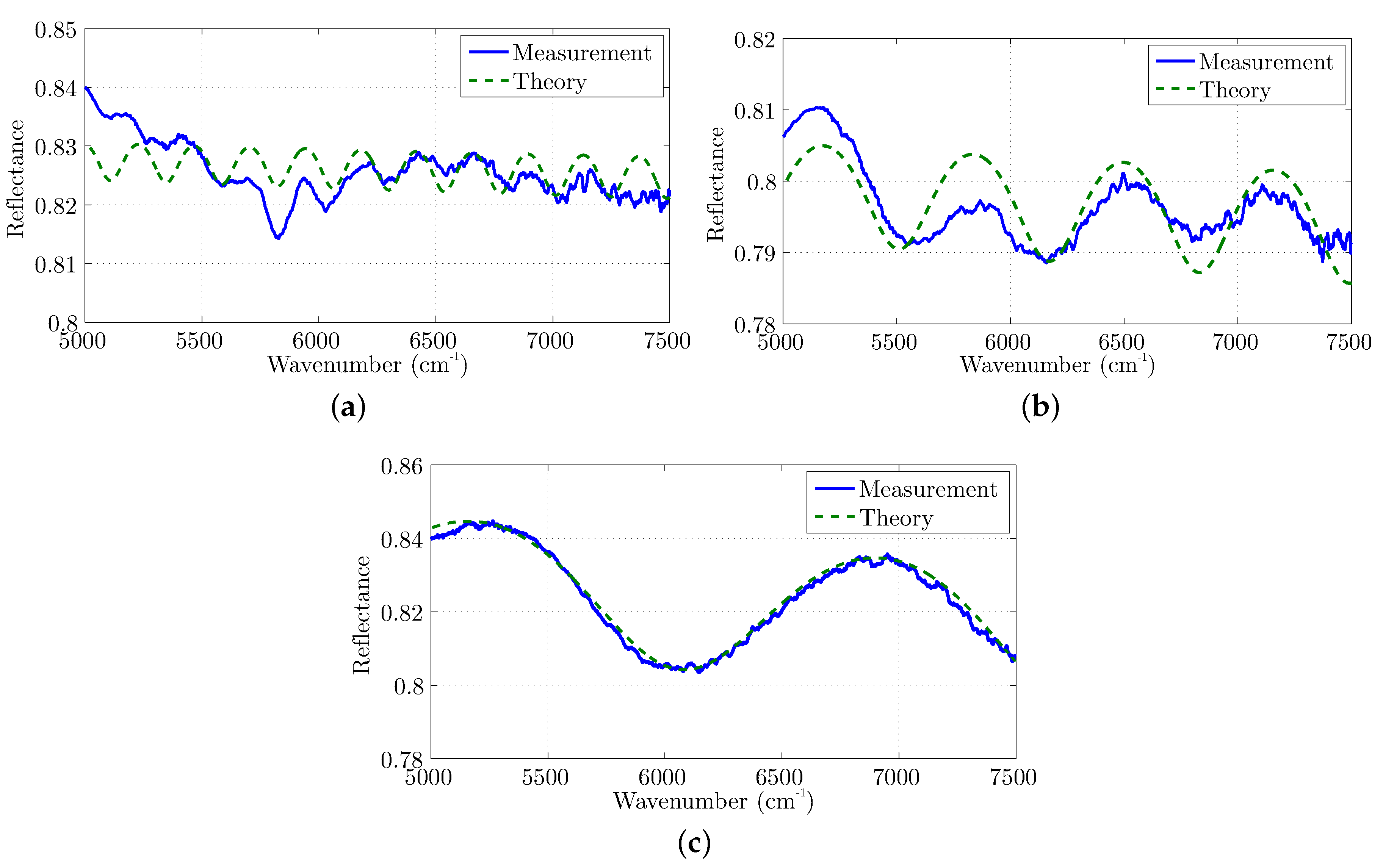
2. Results and Discussion
3. Conclusions
Author Contributions
Acknowledgments
Conflicts of Interest
References
- Kovalenko, M.V.; Scheele, M.; Talapin, D.V. Colloidal Nanocrystals with Molecular Metal Chalcogenide Surface Ligands. Science 2009, 324, 1417–1420. [Google Scholar] [CrossRef] [PubMed]
- Liu, Y.; Gibbs, M.; Puthussery, J.; Gaik, S.; Ihly, R.; Hillhouse, H.W.; Law, M. Dependence of Carrier Mobility on Nano-crystal Size and Ligand Length in Pbse Nanocrystal Solids. Nano Lett. 2010, 10, 1960–1969. [Google Scholar] [CrossRef] [PubMed]
- Moreels, I.; Kruschke, D.; Glas, P.; Tomm, J.W. The Dielectric Function of Pbs Quantum Dots in a Glass Matrix. Opt. Mater. Express 2012, 2, 496–500. [Google Scholar] [CrossRef]
- Maraghechi, P.; Labelle, A.J.; Kirmani, A.R.; Lan, X.; Adachi, M.M.; Thon, S.M.; Hoogland, S.; Lee, A.; Ning, Z.; Fischer, A.; et al. The Donor-Supply Electrode Enhances Performance in Colloidal Quantum Dot Solar Cells. ACS Nano 2013, 7, 6111–6116. [Google Scholar] [CrossRef] [PubMed]
- Gao, Y.; Sandeep, C.S.S.; Schins, J.M.; Houtepen, A.J.; Siebbeles, L.D.A. Disorder Strongly Enhances Auger Recombination in Conductive Quantum-Dot Solids. Nat. Commun. 2013, 4, 2329. [Google Scholar] [CrossRef] [PubMed]
- Kalesaki, E.; Delerue, C.; Morais Smith, C.; Beugeling, W.; Allan, G.; Vanmaekelbergh, D. Dirac Cones, Topological Edge States, and Nontrivial Flat Bands in Two-Dimensional Semiconductors with a Honeycomb Nanogeometry. Phys. Rev. X 2014, 4, 011010. [Google Scholar] [CrossRef]
- Alver, U.; Zhou, W.; Belay, A.B.; Krueger, R.; Davis, K.O.; Hickman, N.S. Optical and Structural Properties of ZnO Nanorods Grown on Graphene Oxide and Reduced Graphene Oxide Film by Hydrothermal Method. Appl. Surf. Sci. 2012, 258, 3109–3114. [Google Scholar] [CrossRef]
- Ip, A.H.; Thon, S.M.; Hoogland, S.; Voznyy, O.; Zhitomirsky, D.; Debnath, R.; Levina, L.; Rollny, L.R.; Carey, G.H.; Fischer, A.; et al. Hybrid Passivated Colloidal Quantum Dot Solids. Nat. Nanotechnol. 2012, 7, 577–582. [Google Scholar] [CrossRef] [PubMed]
- Anderson, N.C.; Hendricks, M.P.; Choi, J.J.; Owen, J.S. Ligand Exchange and the Stoichiometry of Metal Chalco-genide Nanocrystals: Spectroscopic Observation of Facile Metal-Carboxylate Displacement and Binding. J. Am. Chem. Soc. 2013, 135, 18536–18548. [Google Scholar] [CrossRef] [PubMed]
- Sandeep, C.S.S.; Azpiroz, J.M.; Evers, W.H.; Boehme, S.C.; Moreels, I.; Kinge, S.; Siebbeles, L.D.A.; Infante, I.; Houtepen, A.J. Epitaxially Connected PbSe Quantum-Dot Films: Controlled Neck Formation and Optoelectronic Properties. ACS Nano 2014, 8, 11499–11511. [Google Scholar] [CrossRef] [PubMed]
- Manikandan, E.; Kennedy, J.; Kavitha, G.; Kaviyarasu, K.; Maaza, M.; Panigrahi, B.K.; Mudali, U.K. Hybrid Nanostructured Thin-films by PLD for Enhanced Field Emission Performance for Radiation Micro-nano Dosimetry Applications. J. Alloys Compd. 2015, 647, 141–145. [Google Scholar] [CrossRef]
- Huang, D.; Swanson, E.A.; Lin, C.P.; Schuman, J.S.; Stinson, W.G.; Chang, W.; Hee, M.R.; Flotte, T.; Gregory, K.; Puliafito, C.A. Optical Coherence Tomography. Science 1991, 254, 1178–1181. [Google Scholar] [CrossRef] [PubMed]
- Bourquin, S.; Seitz, P.; Salathe, R.P. Optical Coherence Topography Based on a Two-dimensional Smart Detector Array. Opt. Lett. 2001, 26, 512–514. [Google Scholar] [CrossRef] [PubMed]
- Dubois, A.; Moneron, G.; Boccara, A.C. Thermal-light full-field optical coherence tomography in the 1.2 micron wavelength region. Optics Commun. 2006, 266, 738–743. [Google Scholar] [CrossRef]
- Albert, M.; Combs, J. Thickness Measurement of Epitaxial Films by the Infrared Interference Method. J. Electrochem. Soc. 1962, 109, 709–713. [Google Scholar] [CrossRef]
- Dumin, D. Measurement of Film Thickness using Infrared Interference. Rev. Sci. Instrum. 1967, 38, 1107–1109. [Google Scholar] [CrossRef]
- Severin, P. On the Infrared Thickness Measurement of Epitaxially Grown Silicon Layers. Appl. Opt. 1970, 9, 2381–2387. [Google Scholar] [CrossRef] [PubMed]
- Serway, R.A.; Jewett, J.W. Principles of Physics; Saunders College Pub.: Fort Worth, TX, USA, 1998; Volume 1. [Google Scholar]


© 2018 by the authors. Licensee MDPI, Basel, Switzerland. This article is an open access article distributed under the terms and conditions of the Creative Commons Attribution (CC BY) license (http://creativecommons.org/licenses/by/4.0/).
Share and Cite
Mpilitos, C.; Amanatiadis, S.; Apostolidis, G.; Zygiridis, T.; Kantartzis, N.; Karagiannis, G. Development of a Transmission Line Model for the Thickness Prediction of Thin Films via the Infrared Interference Method. Technologies 2018, 6, 122. https://doi.org/10.3390/technologies6040122
Mpilitos C, Amanatiadis S, Apostolidis G, Zygiridis T, Kantartzis N, Karagiannis G. Development of a Transmission Line Model for the Thickness Prediction of Thin Films via the Infrared Interference Method. Technologies. 2018; 6(4):122. https://doi.org/10.3390/technologies6040122
Chicago/Turabian StyleMpilitos, Christos, Stamatios Amanatiadis, Georgios Apostolidis, Theodoros Zygiridis, Nikolaos Kantartzis, and Georgios Karagiannis. 2018. "Development of a Transmission Line Model for the Thickness Prediction of Thin Films via the Infrared Interference Method" Technologies 6, no. 4: 122. https://doi.org/10.3390/technologies6040122