Article

Channel Engineering for Nanotransistors in a Semiempirical Quantum Transport Model

1
Department of Physics, Brandenburgische Technische Universität Cottbus/Senftenberg, Fakultät 1, Postfach 101344, 03013 Cottbus, Germany
2
Institute of Physics, Academy of Sciences of the Czech Republic, Cukrovanická 10, 162 53 Praha 6, Czech Republic
3
Gesellschaft zur Förderung von Wissenschaft und Wirtschaft Frankfurt, Im Technologiepark 1, 15236 Frankfurt (Oder), Germany
4
Globalfoundries Dresden, Wilschdorfer Landstraße 101, 01109 Dresden, Germany
*
Author to whom correspondence should be addressed.
Mathematics 2017, 5(4), 68; https://doi.org/10.3390/math5040068
Submission received: 28 September 2017 / Revised: 10 November 2017 / Accepted: 14 November 2017 / Published: 22 November 2017

Abstract

:
One major concern of channel engineering in nanotransistors is the coupling of the conduction channel to the source/drain contacts. In a number of previous publications, we have developed a semiempirical quantum model in quantitative agreement with three series of experimental transistors. On the basis of this model, an overlap parameter 0 C 1 can be defined as a criterion for the quality of the contact-to-channel coupling: A high level of C means good matching between the wave functions in the source/drain and in the conduction channel associated with a low contact-to-channel reflection. We show that a high level of C leads to a high saturation current in the ON-state and a large slope of the transfer characteristic in the OFF-state. Furthermore, relevant for future device miniaturization, we analyze the contribution of the tunneling current to the total drain current. It is seen for a device with a gate length of 26 nm that for all gate voltages, the share of the tunneling current becomes small for small drain voltages. With increasing drain voltage, the contribution of the tunneling current grows considerably showing Fowler–Nordheim oscillations. In the ON-state, the classically allowed current remains dominant for large drain voltages. In the OFF-state, the tunneling current becomes dominant.

1. Introduction

At this time, transistors in integrated circuits are projected with channel lengths below 10 nm. At this length scale quantum transport plays a substantial role. Microscopic modeling of the drain current of such a nanotransistor thus requires the evaluation of the wave functions of the charge carriers [1,2,3,4,5,6,7,8,9,10] or the evaluation of Greens functions [11,12,13,14,15,16,17,18,19,20,21,22]. Because of the considerable effort for such microscopic calculations, there is a need for more flexible compact modeling like BSIM (Berkeley Short-channel IGFET Model) [23,24,25,26,27], the virtual source model [28,29,30,31,32,33] or wave function-based models [1,5,7,34,35,36,37,38,39,40]. In this paper, we focus on the latter approach in which the microscopic wave functions of the charge carriers are approximated in a compact form.
A microscopic calculation of the wave functions of the charge carriers requires the time-consuming numerical solution of the Schrödinger equation in at least two relevant dimensions (along the conduction channel and perpendicular to the semiconductor-insulator interface). To move towards a compact quantum model, an essential step is therefore the formulation of a one-dimensional effective model, which can be constructed and evaluated quickly. In our approach, we start from a complete three-dimensional microscopic R-matrix-description of a nanotransistor in the Landauer–Büttiker formalism and reduce it systematically to a one-dimensional effective model [5,37]. Here, one assumes a separable form of the scattering potential in the conduction channel with only a single relevant mode (‘single level approximation’). The resulting one-dimensional effective model is microscopically justified for the OFF-state and for the threshold voltage region, which are essential for complementary logic. Assuming furthermore a piecewise linear potential, the effective model can be formulated in a scale-invariant form using only five dimensionless transistor parameters [38]. These transistor parameters describe the height of the source-drain barrier, the device temperature, the channel length and the applied drain voltage. The fifth parameter, the overlap parameter 0 C 1 , is particularly relevant for channel engineering because it gives a criterion for the quality of the coupling between the contacts and the conduction channel: a high level of C means good matching properties (low reflection) between the wave functions in the source/drain contact and in the conduction channel. In a model with equal transverse confinement in the contacts and in the conduction channel as in [35,36], one has C = 1 . Finally, assuming the applicability of our theoretical results in the piecewise linear potential approximation, the described five transistor parameters are adjusted to the experimental traces [39,40]. Excellent agreement between theory and experimental traces is found for three series of transistors (‘A-, B- and C-transistors’) fabricated and measured by Globalfoundries with gate lengths of 30 nm, 26 nm and 22 nm.
This paper contains a detailed study of the overlap parameter of the C-transistors. We relate the results for the overlap parameter to the sub-threshold slope and to the saturation current in the experimental transfer characteristics. Here, we also compare the present results for the C-transistors with previous results for the A-transistors with a much poorer overlap parameter and a poorer saturation current. It is found that a large overlap parameter is associated with a large sub-threshold slope in the transfer characteristic and a high saturation current in the ON-state. The magnitude of the saturation current turns out to be strongly influenced by the magnitude of a characteristic jump in the overlap parameter occurring at the threshold voltage. This jump is particularly pronounced for short channel devices and for low temperatures. It is probably a non-linear phenomenon resulting from the Coulomb interaction, which determines the potential in the shallow junction extensions between the contacts and conduction channel. At low temperatures, thermal random motion is reduced and screening is improved, and one expects a smooth transition between the contacts and the conduction channel.
With future device miniaturization in mind, we analyze the contribution of the tunneling current to the total drain current. Taking the C-transistor with the intermediate gate length of 26 nm as an example it is seen that for all gate voltages, the share of the tunneling current becomes small for small drain voltages. With increasing drain voltage, the contribution of the tunneling current grows considerably showing Fowler–Nordheim oscillations. In the ON-state, the classically-allowed current remains barely dominant for large drain voltages. In contrast, in the OFF-state, the drain current becomes nearly entirely a tunneling current for large drain voltages.

2. Semiempirical Transistor Model

Our semiempirical model is reviewed in detail in the Appendix A. This section contains only an account of the central equations in a nut-shell.

2.1. Scale-Invariant Drain Current

In [39,40], a formula for the drain current of a nanotransistor per width J is derived as given by:
j = J J 0 = C 0 d ϵ s ( ϵ m ) s ( ϵ m + v D ) T e f ( ϵ ) j ( v 0 , u , C , v D , l ) .
Here, one has five dimensionless transistor parameters v 0 = V 0 / E F (effective barrier height), u = k B T / E F (normalized device temperature), C (wave function overlap; for the microscopic interpretation, see Equation (A19)), l = L / λ (effective channel length) and v D = e U D / E F (normalized drain voltage), where L is the channel length of the transistor, λ = / 2 m * E F is the scaling length and U D is the applied drain voltage. For the microcopic interpretation of the energy ϵ see Equation (A26). While the three transistor parameters v 0 , u and C result from a fit of the experimental output characteristics (see the next section), the remaining quantities can be calculated assuming that the Fermi energy in the source contact E F and the chemical potential μ ( T ) are known from the doping concentration: modeling the contacts as a homogeneous three-dimensional electron gas appropriate for a wide transistor with a large junction depth, one has:
m = μ E F = u X 1 / 2 4 3 π u 3 / 2
where X 1 / 2 is the inverse function of the Fermi–Dirac integral of order 1 / 2 . Furthermore, we adopt from [37,38] values for the current normalization constant J 0 = 2 e N v c h E F / ( h λ ) 50 mA/ μ m with the valley degeneracy N v c h in the conduction channel, for the characteristic length λ 1 nm and for the Fermi energy in the source E F = 0.35 eV. This way, for the investigated devices, the effective channel length l is given by the channel length in nanometers. The supply function is calculated from:
s ( α ) = u 4 π F 1 2 α u ,
where F 1 / 2 is the Fermi–Dirac integral of order 1 / 2 . The supply function gives the number of occupied scattering states per energy interval and per channel width. The effective current transmission T e f is calculated from the scattering solutions of a normalized one-dimensional effective Schrödinger equation in the scaled x-coordinate x ^ = x / L x :
1 l 2 d 2 d x 2 + v e f ( x ) ϵ ψ e f ( x ) = 0
with the effective potential given by:
v e f ( x ) = 0 for x < 0 v 0 v D x for 0 x 1 v D for x 1 .
For the microscopic interpretation of the effective potential, see Equation (A22). The effective potential of height v 0 is plotted in Figure 1b. The source-incident scattering solution of (4) takes the asymptotic form:
ψ e f ( x < 0 ) = e i k 1 x + r e f e i k 1 x with k 1 = l ϵ
and:
ψ e f ( x > 1 ) = t e f e i k 2 x with k 2 = l ϵ + v D .
It now holds that T e f = k 2 | t e f | 2 k 1 1 (see Equation (A25)).
From the effective Schrödinger Equation (4), it is clear that contributions to T e f with ϵ < v 0 are due to source-drain tunneling. Typical forms for the effective current transmission and the supply function in (3) are given in Figure 8, and they are illustrated in Figure 1c: As is well known, T e f approaches zero for ϵ v 0 and approaches unity for ϵ v 0 . Since at room temperature, the thermal energy k B T is considerably smaller than E F , the supply function decays quickly for ϵ > m . As a consequence, in the OFF-state with v 0 > m 1 , which is illustrated in Figure 1, there is only a small overlap between the two factors s ( ϵ m ) s ( ϵ m v D ) and T e f ( ϵ ) in (1), and the total drain current becomes small.

2.2. Calibration of the System Parameters

It is seen from Equation (1) that the normalized current per width j can be calculated from five transistor parameters v 0 , u , C , v D and l. From the measurements of J, U D and L, one obtains directly the three parameters j, v D and l from the values for J 0 , E F and λ , which are adopted from [37,38]. To find the three missing transistor parameters v 0 , u and C in Equation (1), we assume the existence of three calibration functions v 0 ( U G ) , u ( U G ) and C ( U G ) depending only on the experimental gate voltage U G . Through these calibration functions, the drain current becomes dependent on U G . The calibration functions result from the minimization of the root mean square deviation:
Δ J r m s ( U G ) = 1 N i N J e x p ( U D i , U G ) J t h ( U D i , v 0 , u , C ) J e x p ( U D i , U G ) 2
at given U G . Here, J e x p ( U D i , U G ) is the experimental current measured at N equidistant drain voltages U D i . The theoretical current is calculated from (1) as:
J t h ( U D i , v 0 , u , C ) = J 0 j ( v 0 , u , C , v D = q U D i / E F , l = L / λ ) .
The values of the parameters v 0 , u and C that lead to the minimum of Δ J r m s ( U G ) constitute the calibration functions v 0 ( U G ) , u ( U G ) and C ( U G ) . One obtains the calibrated theoretical current plotted in Figure 2 and Figure 3 as:
J c a l ( U D , U G ) = J t h [ v 0 ( U G ) , u ( U G ) , C ( U G ) , q U D / E F , L / λ ] .

3. The Calibration Functions

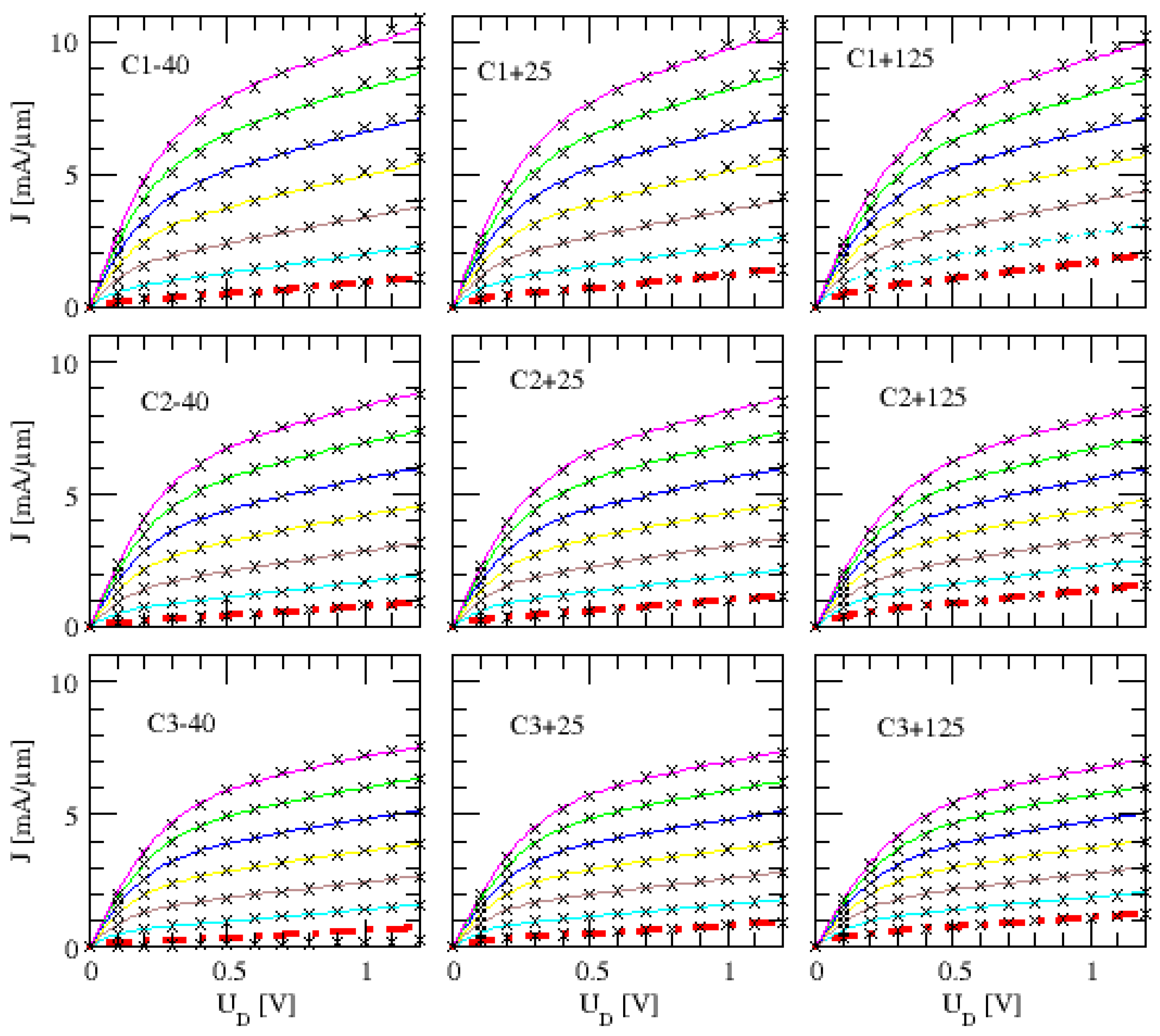
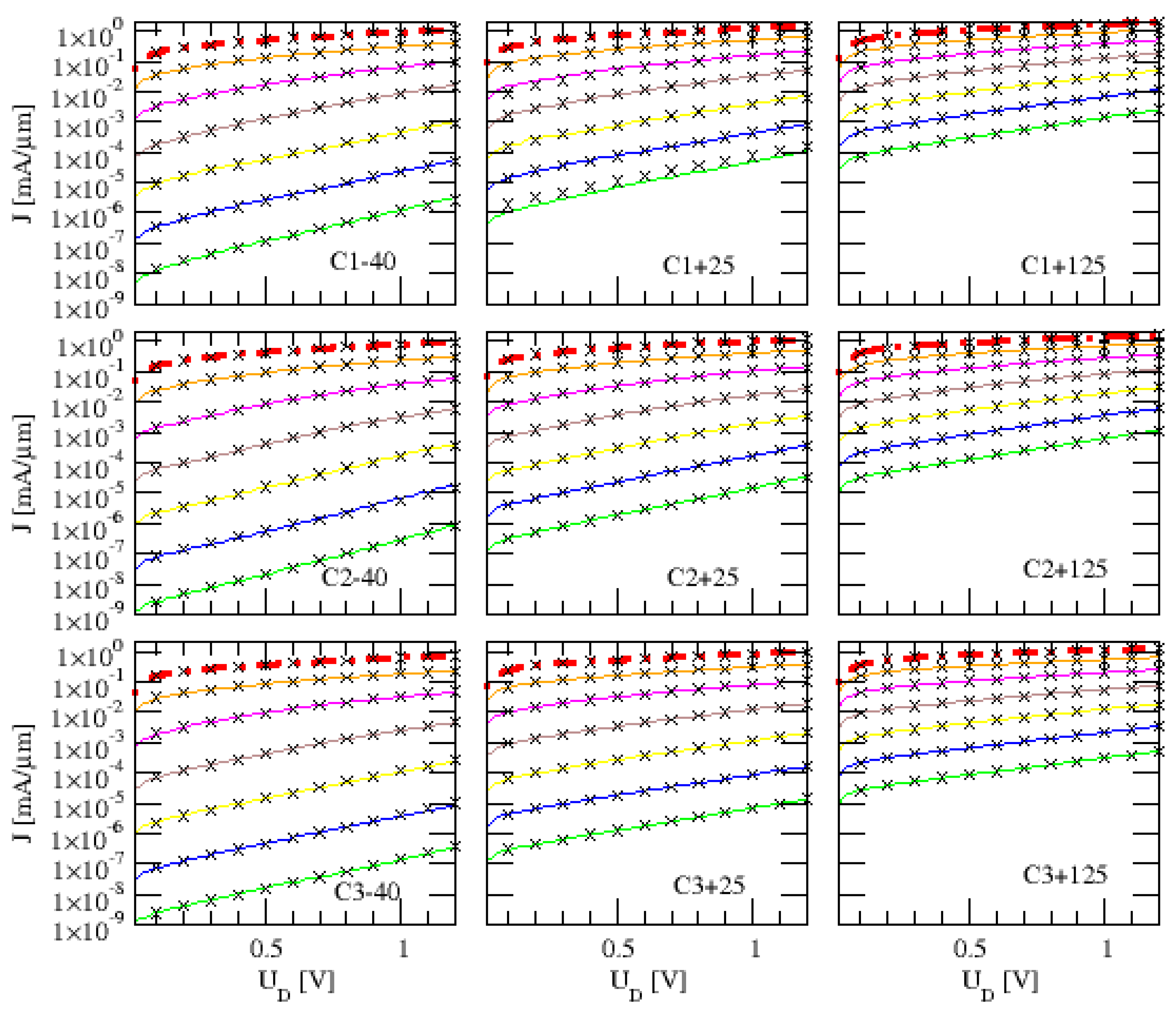
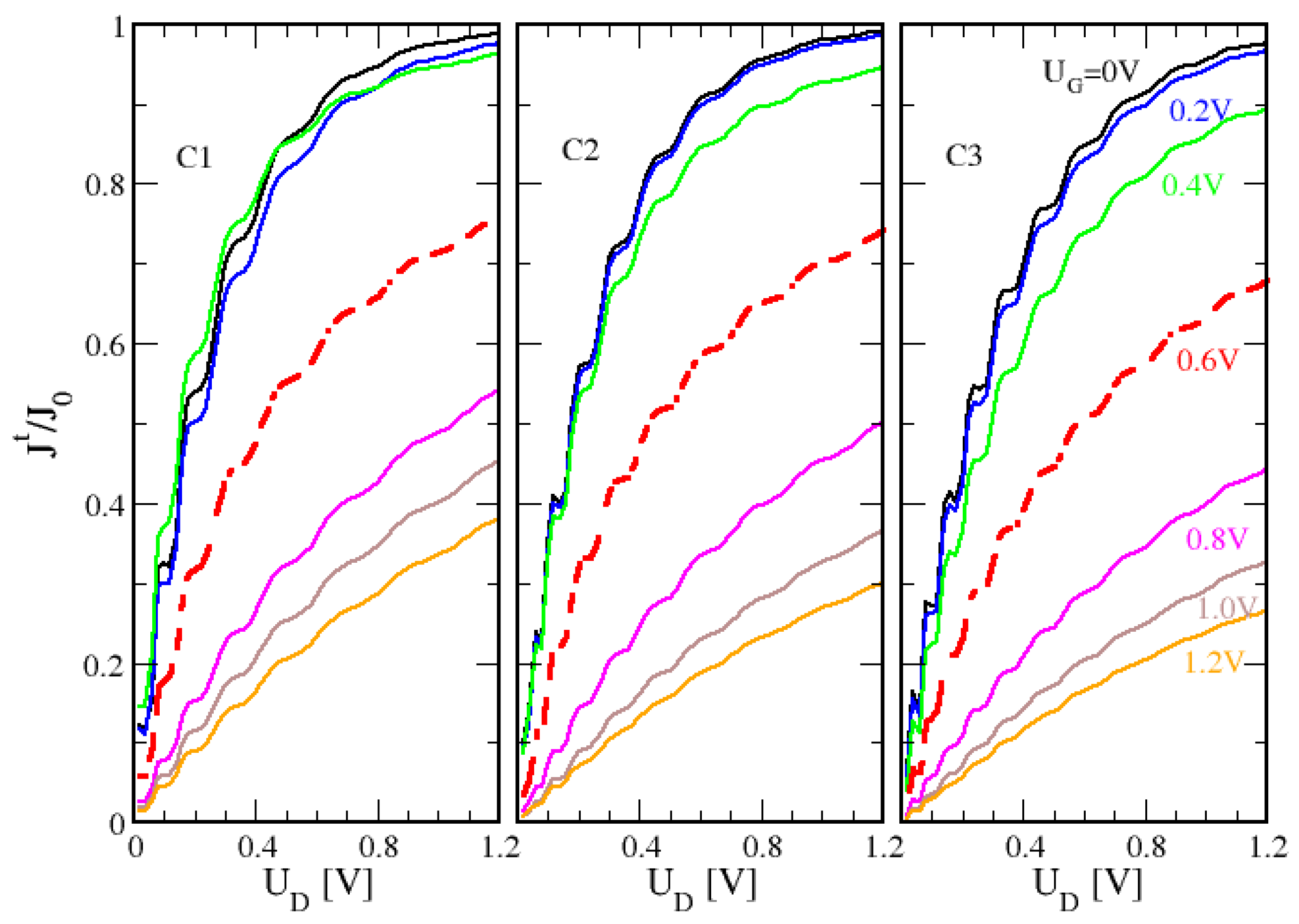
3.1. Experimental and Theoretical Output Characteristic

We analyze the experimental and theoretical output characteristics of a series of three n-channel transistors (‘C-transistors’) with gate lengths of L = 22 nm (C1), L = 26 nm (C2, identical to B3 in [40]) and L = 30 nm (C3, identical to B4 in [40]). The characteristics are plotted in Figure 2 and Figure 3 for three environment temperatures T = 233 K, 298 K and 398 K [41]. In all cases, excellent agreement between experiment and theory is found. The threshold gate voltage for the C-transistors we locate at U G t h = 0.6 V where the ID-VD traces show a close to linear behavior. As usual, in the ON-state, the drain current grows weaker than linearly with increasing drain voltage showing a negative bending. In contrast, in the OFF-state, the drain current grows faster than exponentially with the drain voltage at small drain voltages and exponentially at larger drain voltages leading to a positive bending. These results for the OFF-state have already been reported in [39,42] for another series of transistors. In agreement with our theoretical results in [38], the slope of the close to linear threshold trace is found to decrease slightly with channel length and to increase slightly with temperature.
The location of U G t h around 0.6 V is confirmed, first by an inspection of the temperature dependence of the drain current and, second, by an inspection of the calibration functions: Above U G t h , in the ON-state (see Figure 2), the output characteristics are only weakly temperature dependent [43]. In contrast, below U G t h , in the OFF-state (see Figure 3), the drain current increases strongly with increasing temperature, which suggests thermal activation. This contrast is consistent with the metallic characteristics of conduction in the ON-state and its insulator characteristic in the OFF-state.
The inspection of the calibration functions yields: First, above U G t h , the barrier height parameter v 0 falls below the chemical potential m indicating classically allowed transport without thermal activation, while below, U G t h we have v 0 > m (see Figure 4). Second, above U G t h , the device temperature parameter u increases strongly with increasing gate voltage (see Figure 4), while below U G t h , the device temperature stays around the environment temperature. Third, the overlap parameter C takes a jump at U G t h (see Figure 5).

3.2. The Calibration Functions for Barrier Height and Device Temperature

The calibration functions for the barrier height and for the device temperature of the three C-transistors are shown in Figure 4 for the three environment temperatures. The general structure is the same in all cases and coincides with the one reported in [39,40]: In the OFF-state, for gate voltages below U G t h , the barrier height lies above the chemical potential m in the source and drops as a nearly linear function of the gate voltage, v 0 ( U G ) 2 2 U G [ V ] . At U G t h , one has v 0 m , and the conduction channel becomes strongly populated. For gate voltages above U G t h , in the ON-state, the drop of v 0 ( U G ) is much weaker than in the OFF-state. This we attribute to better screening when the conduction channel is populated. As can be expected, the screening effect is most pronounced in the shortest channel device C1 at low temperatures. Here, the barrier height remains roughly constant in the entire ON-state regime in spite of the increased applied gate voltage. As a further consequence of the changed screening conditions in the ON-state, we adduce the jump in the overlap calibration function C of the transistors at U G t h (see Figure 5), which is by far most pronounced for C1 at low temperatures. In an intuitive physical picture, we explain the reduction of screening at higher temperatures invoking increased random thermal motion: because of Poisson’s equation, screening of an external potential requires a specific adjustment of the electron density. This adjustment is prevented by Pauli’s exclusion principle in small dimensions, on the one hand, and by random thermal motion, on the other.
For all examined transistors and environment temperatures, the device temperature stays close to the environment temperature in the OFF-state due to small ohmic heating. A careful inspection of Figure 4 shows that the device temperature generally increases slightly when increasing the environment temperature. Above the threshold, the drain current sets in, and Ohmic heating leads to rising device temperatures. At E F 0.35 eV, one has at room temperature 298 K the value k B T / E F 0.075 . The temperature difference Δ T = 398 K − 298 K corresponds to k B Δ T / E F 0.025 .

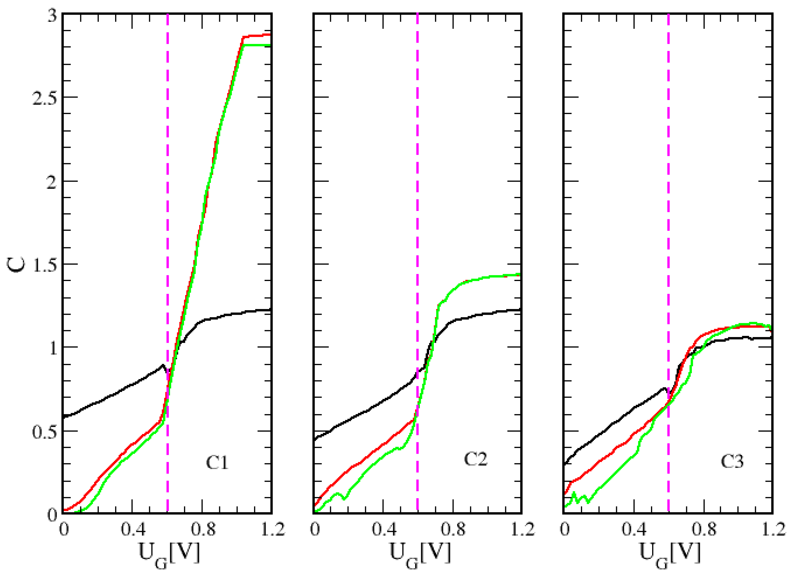
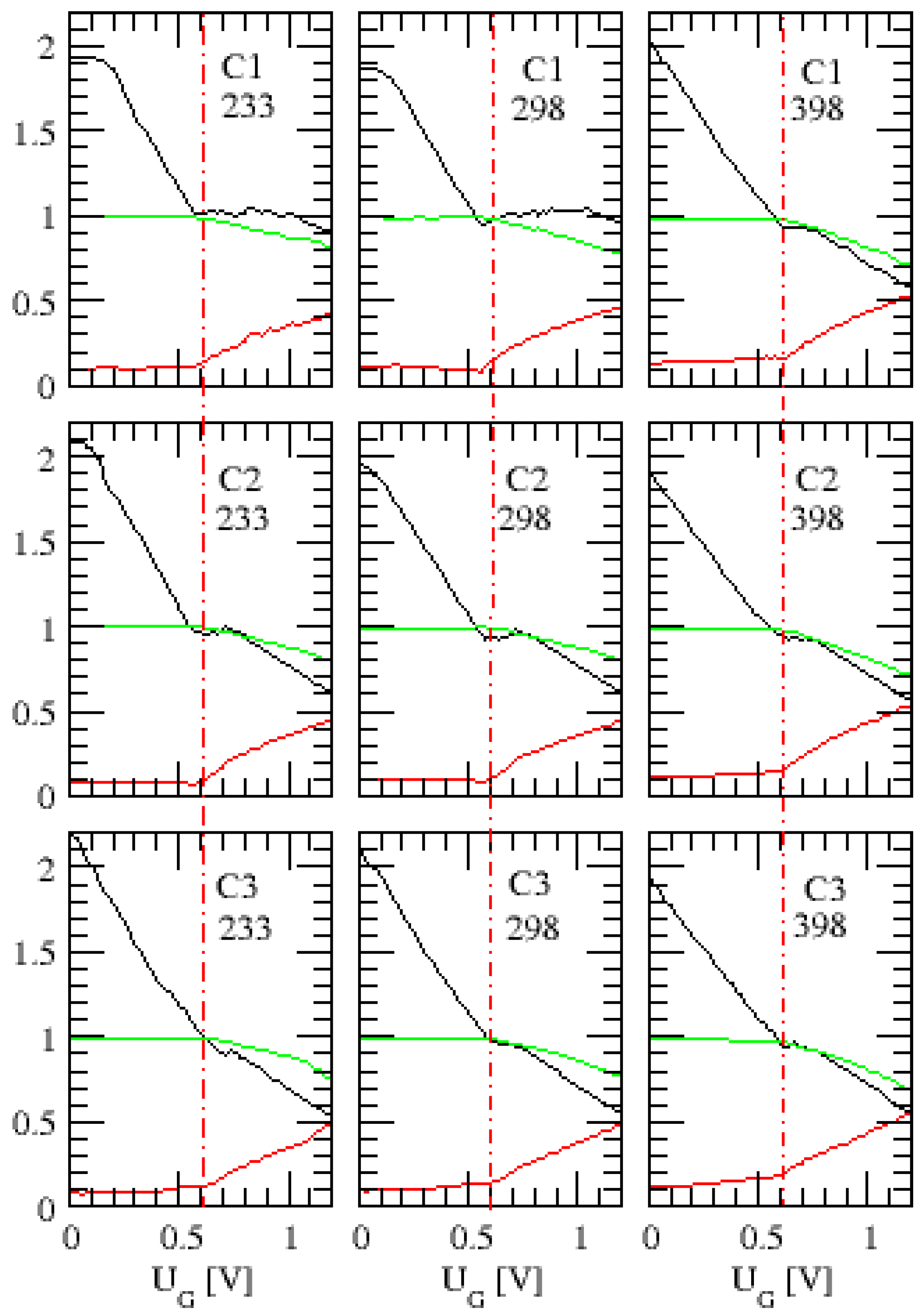
3.3. The Calibration Function for the Overlap Parameter and Transfer Characteristic

In Figure 5, the calibration function of the overlap parameter (‘overlap function’) is depicted. In all cases, the overlap function is a growing function of the gate voltage showing a jump at U G t h , which is most pronounced at low temperatures and short channel lengths. As mentioned, these properties can be explained by improved screening conditions with increasing population of the conduction channel. The fact that C takes values greater than unity above the threshold gate voltage indicates that at least one excited mode at the interface plays a role above the threshold so that the single-level approximation leading to Equation (A19) is not strictly applicable any more. In the screening picture, it can also be explained that in the OFF-state, the overlap functions of all C-transistors at the low temperatures of T = 233 K and T = 298 K take very small values and are nearly the same. This is consistent with the expectation that in the OFF-state, the population of the conduction channel is nearly absent at low temperatures (‘no screening limit’). Furthermore, in the OFF-state, for all C-transistors, the overlap parameter is much larger at the high temperature of T = 398 K. This we attribute to the thermally-activated population of the channel. In contrast, in the ON-state for all C-transistors, the overlap parameter is smaller at the high temperature due to the less pronounced jump in C at the threshold voltage. This we attribute to random thermal motions degrading the screening properties of the strongly populated ‘metallic’ conduction channel.
In Figure 6a, we compare the overlap functions of the three A-transistors Ai, i = 1 , 2 , 3 taken from [39] to the ones of the C-transistors Ci, i = 1 , 2 , 3 at the room-environment temperature. Here, Ai has the same channel length as Ci. In the OFF-state, the temperature parameters of both the A- and the C-transistors are close to room-environment temperature, and the barrier height parameter of both the A- and the C-transistors is given by v 0 ( U G ) 2 2 U G [ V ] . Therefore, in the OFF-state, the essential differences between the A- and the C-transistors lies in the overlap parameter. In Figure 6b, we also include the transfer characteristics of the A- and C-transistors to find relations between features in the overlap function and the transfer characteristics of the devices. It is observed that for small gate voltages the overlap functions of the A- and C-devices are very similar and that the transfer characteristics are close to each other. With increasing gate voltage, the overlap parameters of the C-devices increase while those of the A-devices stay constant. As a consequence, the slope of the transfer characteristics of the C-devices exceeds that of the A-devices leading to a larger drain current of the C-transistors. At the threshold, a strong Coulomb coupling between the contacts and the conduction channel leads to the described jump in the overlap parameter of the C-transistors. In contrast, in the A-devices, the increase in the overlap parameter around the threshold is gradual and not so pronounced. As a consequence, the saturation current in the C-devices is markedly larger than that of the A-devices. The comparison between the A- and the C-transistors therefore indicates that a large overlap factor leads to large slopes of the transfer characteristic in the OFF-state and to large saturation currents in the ON-state. This finding suggests that the overlap factor might serve as a quantitative criterion of a systematic classification of nanotransistors in the future.

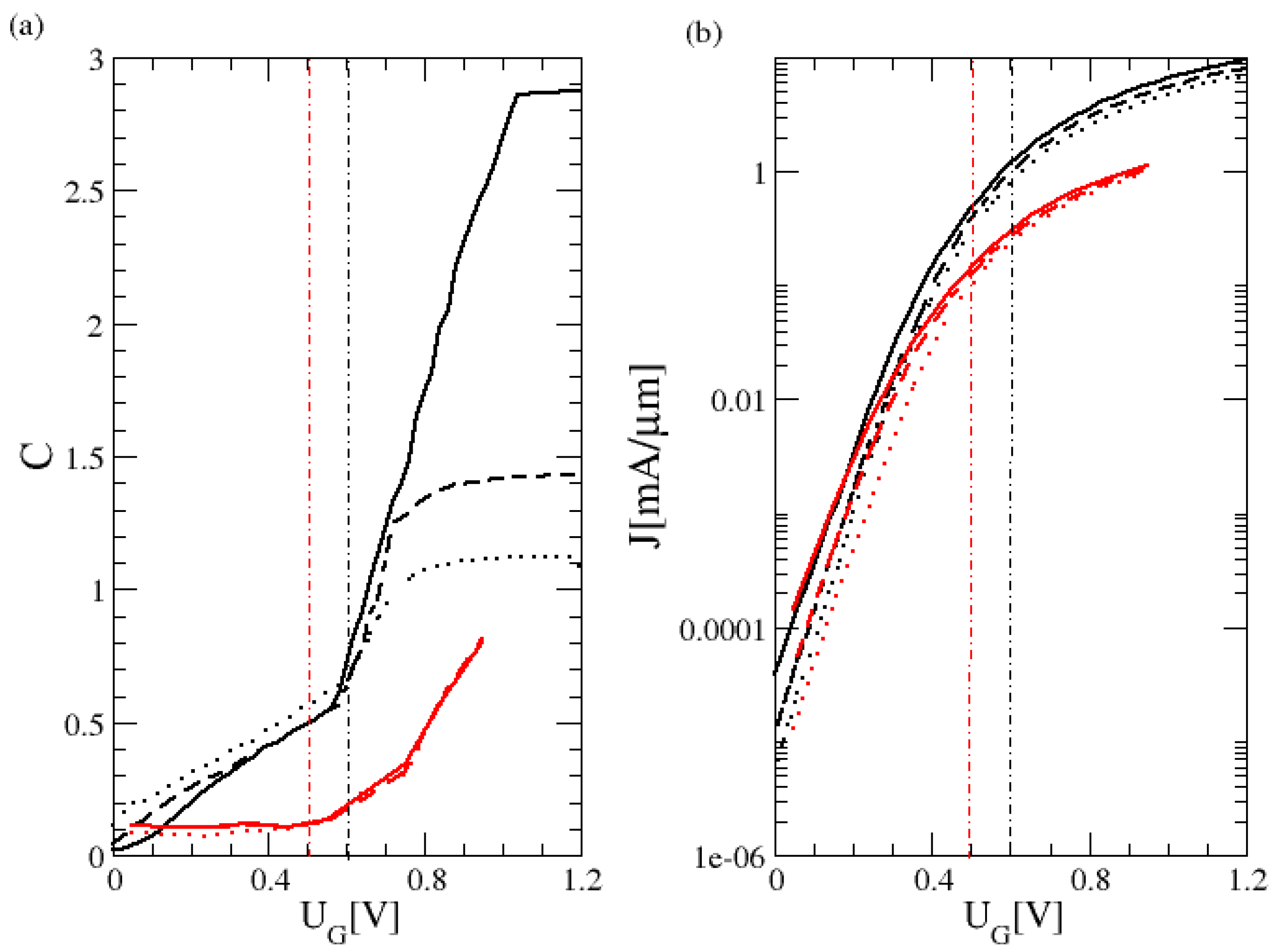
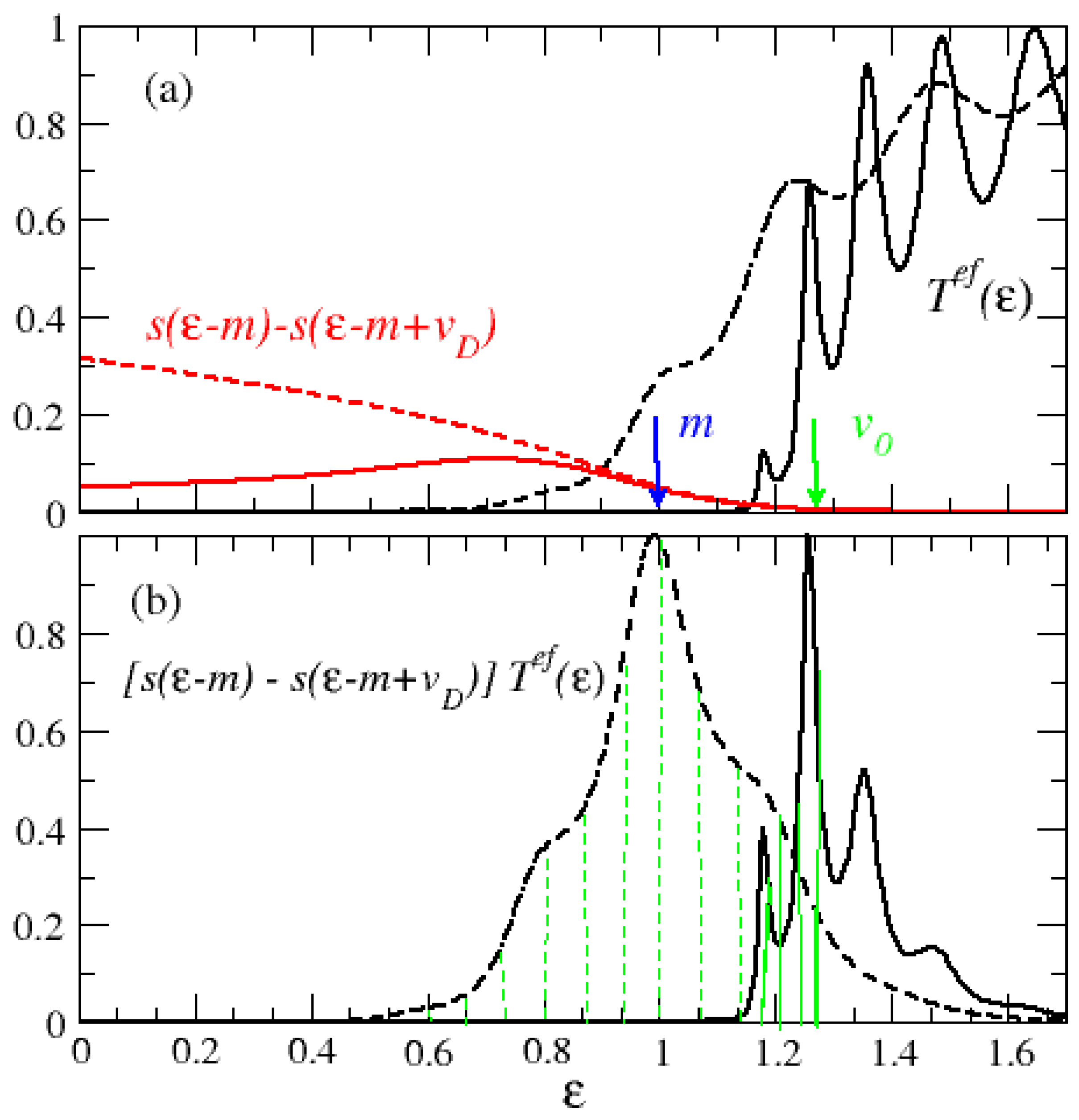
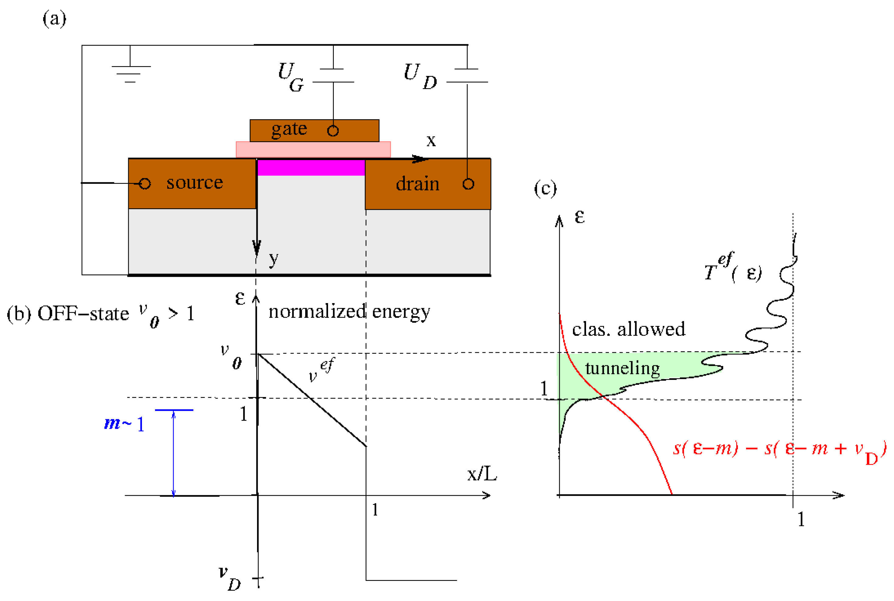
4. Tunneling Current

In Figure 7, we plot the classically forbidden tunneling part of the drain current:
J t = C J 0 0 v 0 d ϵ s ( ϵ m ) s ( ϵ m + v D ) T e f ( ϵ )
normalized to the total current in Equation (1) (see the green area in Figure 1c). As can be expected, the share of the tunneling current J t always decreases with increasing the gate voltage, increases with increasing the drain voltage and decreases with increasing channel length. It is seen that for all gate voltages and channel lengths, the contribution of J t becomes small for small drain voltages. With increasing drain voltage, the contribution of the tunneling current grows, showing oscillations. These oscillations arise from Fabry–Perot-type resonances in the transmission (see [44] and Figure 8). As can be taken from Figure 2 and Figure 3, the Fabry–Perot-type resonances are averaged out efficiently in the energy integral in (1) to determine the total drain current j at the experimental temperatures. However, due to the abrupt upper limit v 0 of the energy integration in (11), the tunneling current is discernibly increased whenever a Fabry–Perot resonance falls below v 0 corresponding to the inset of resonant Fowler–Nordheim tunneling (see Figure 3 of [44]). The resulting oscillations in J T are probably overestimated in the abrupt barrier potential in Equation (5). In the OFF-state, i.e., for the gate voltages below U G t h , one finds a rise of J t / J 0 for all transistors up to well above 80 % for V D 0.5 V. Above U G t h , one finds a weaker rise of J t / J 0 for all transistors, which still ranges between 20 % and 50 % for V D 0.5 V.
We analyze the strong increase of J t / J 0 with increasing drain voltage in the OFF-state. For this purpose, the constituents of the integrand in (11) are plotted in Figure 8 for a small drain voltage and for a large drain voltage. These constituents are the effective current transmission T e f and the difference of the supply functions in source and drain contact s ( ϵ m ) s ( ϵ m v D ) (‘supply function difference’), which show the general behavior discussed in Figure 1. Comparing the results for the small drain voltage to the ones at the large drain voltage, one finds: First, the supply function difference is always larger for the large drain voltage, though this difference is small in the range of relevant energies where T e f is finite. Second, and most important, for the large drain voltage, T e f sets in at much smaller energies, so that it is much larger than T e f for the small drain voltage in the range of tunneling-energies below v 0 . As a consequence of these two findings, the product function is larger and wider for the large drain voltage, yielding a much larger value for J t in (11).

5. Conclusions for Channel Engineering

The comparison between the A- and C-devices in Figure 6 suggests that the coupling between the contacts and the channel is of great importance for the switching properties of a transistor. One expects that the quality of this coupling sensitively depends on the doping profile in the shallow junction extension. Here, an important factor are the screening properties arising in the doping profile. In the C-transistors, a good contact-to-channel coupling exists leading to a growing population of the conduction channel in the OFF-state when approaching the threshold voltage through thermal excitation. This causes a significant increase of the sub-threshold slope in the transfer characteristic. Moreover, at good channel coupling, a jump in the overlap factor arises at the threshold voltage causing a large saturation current in the ON-state. This jump in the overlap factor is most likely a non-linear phenomenon resembling a metal-insulator transition. Therefore, for the theoretical investigation of an optimal doping profile in the shallow junction extension, a calculation of the Coulomb interaction at least in the Hartree approximation is necessary, which is left to future research.

Acknowledgments

J.K. acknowledges support of the Grant Agency of the Czech Republic, grant No. 14-37427G.

Author Contributions

Theoretical development and interpretation done by U.W., J.K. and H.R., experimental data provided by M.H., M.W. and J.H. Furthermore, U.W. provided the computer software.

Conflicts of Interest

The authors declare no conflict of interest.

Appendix A. Review of the Semiempirical Model

Appendix A.1. Single-Level Abrupt Transition Approximation (SMAT)

In the abrupt transition approximation, one assumes that the potential acting on the charge carriers has in three dimensions the general form:
V ( r ) = V 1 ( y , z ) for x 0 V T ( y , z ) + V L ( x ) for 0 x L V 2 ( y , z ) e U D for x L .
There are two abrupt transitions in the potential, the first between the source contact ( x 0 , see Figure 1) and the conduction channel ( 0 x L ) and the second between the conduction channel and the drain contact ( x L ). Because of the separable form of the potential, the wave functions in the conduction channel can be expanded in modes (‘channel modes’):
Ψ ( 0 < x < L , y , z ; E ) = k α k ψ k ( x ) ϕ k ( y , z )
with general expansion coefficients α k . Here, the transverse functions of the channel modes are defined by:
2 2 m * d 2 d y 2 + d 2 d z 2 + V T ( y , z ) E k T ϕ k ( y , z ) = 0
and the longitudinal functions by:
2 2 m * d 2 d x 2 + V L ( x ) + E k T E ψ k ( x ) = 0 .
In the source contact, we obtain a similar expansion in modes (‘contact modes’):
Ψ ( x < 0 , y , z ; E ) = n a 1 , n e i k 1 , n x + b 1 , n e i k 1 , n x Φ n ( y , z ) .
with general expansion coefficients a 1 , n and b 1 , n . In the drain, one has:
Ψ ( x > L , y , z ; E ) = n a 2 , n e i k 2 , n x + b 2 , n e i k 2 , n x Φ n ( y , z )
with general expansion coefficients a 2 , n and b 2 , n . Here, the case of identical contacts V 1 ( y , z ) = V 2 ( y , z ) = V ( y , z ) is taken where the identical transverse functions of the contact modes are given by:
2 2 m * d 2 d y 2 + d 2 d z 2 + V ( y , z ) E n Φ n ( y , z ) = 0 .
The wave numbers in the longitudinal direction are given by:
k s , n = 2 m * ( E E n + W s ) ,
with the contact index s = 1 for the source and s = 2 for the drain, so that W 1 = 0 and W 2 = e U D . For E < W s E n , it results that k s , n is imaginary, and the corresponding contact mode is evanescent and carries no current. In our generic transistor model, we introduce a lateral cut-off for the wave functions:
Ψ ( x , 0 , z ; E ) = Ψ ( x , D , z ; E ) = Ψ ( x , y , 0 ; E ) = Ψ ( x , y , W ; E ) = 0
carrying through to the transverse functions in the conduction channel and in the contacts.
In the derivation of the single mode approximation (SMA) in [5], it was assumed that the conduction channel is narrow in both transverse directions so that only the lowest channel mode with k = 0 has to be taken into account (single-mode abrupt transition approximation in the strict sense). However, usually, in bulk nano-FETs and thin film transistors, one has a wide channel, i.e., the conduction channel is narrow only in one transverse direction (here, depth direction = y-direction) and wide in the other transverse direction (here, the width direction = z-direction). Then, a number of relevant channel modes has to be taken into account. For this purpose, in [38], the potential in (A1) is assumed to be independent of z, leaving V ( y , z ) = V ( y ) , V L ( y , z ) = V L ( y ) and V T ( y , z ) = V T ( y ) . The confinement in the z-direction is only represented by the wave function cut-off (A9). One then obtains from (A3) transverse modes in the channel of the form:
ϕ k ( y , z ) = ϕ k y , k z = ζ k y ( y ) sin k z π W z
with:
2 2 m * d 2 d y 2 + V T ( y ) E k y T y ζ k y ( y ) = 0
and:
E k y , k z T = E k y T y + 2 2 m * k z π W 2 .
For a bulk nano-FET, the functions ζ k y ( y ) can be identified with the sub-band functions in an MOS-structure, as calculated, for example, in [45]. For thin film transistors, the sub-band functions ζ k y ( y ) are strongly influenced by the wave function cut-off at y = D . In the single-mode approximation for wide channels, one takes into account in the scattering matrix the channel modes with k y = 0 and k z N , i.e., in the depth direction only contributions from the lowest sub-band ζ 0 ( y ) are kept, while in the z-direction, all k z are summed over. For the identical contacts, we find in analogy to (A10):
Φ n ( y , z ) = ϕ n y , n z = Φ n y ( y ) sin n z π W z
with:
2 2 m * d 2 d y 2 + V T ( y ) E n y y Φ n y ( y ) = 0
and:
E n y , n z = E n y y + 2 2 m * n z π W 2 .

Appendix A.2. Drain Current and Effective Current Transmission

The drain current I D was calculated in [39,40], introducing the further approximation:
k s , n k s e f = 2 m * ( E E 0 + W s )
where E 0 = E 0 y + ( 2 / 2 m * ) ( π / W ) 2 is the smallest solution of the eigenvalue problem in (A7).
It was found that:
I D = N v c h 2 e h 0 d E x y C ( E x y ) S ( E x y μ ) S ( E x y μ + e U D ) T e f ( E x y ) ,
where E x y is the conserved energy in the x y -plane, and the valley degeneracy in the conduction channel N v c h is included. The summation over occupied scattering states with different total energy E, but the same E x y is carried out in the formation of the supply function:
S ( α ) = n z f α + 2 2 m * π n z W 2 = 1 4 π u w F 1 / 2 α k B T ,
with the Fermi distribution f ( x ) = ( e x / k B T + 1 ) 1 and the normalized transistor width w = W / λ . In the last step, the limit W was taken. At constant E x y , the scattering states are characterized by the index n y of the incident transverse mode. The overlap function:
0 C ( E x y ) = n y n y ζ n y 2 ζ n y 2 Θ E x y 2 2 m * n y π D 2 Θ E x y + e U D 2 2 m * n y π D 2 1
results from summing up the drain current contributions coming from the incident channels n y and the transmitted channels n y . Here, the theta functions ensure that only propagating modes are taken into account. An upper bound for C ( E x y ) can be obtained ignoring the theta functions. Then, one obtains from the normalization of the sub-band functions C ( E x y ) = 1 . It is seen that in C ( E x y ) , the products of squares of the projection factors:
ζ n y = 0 D d y Φ n y ( y ) ζ 0 ( y )
are summed over so that C ( E x y ) 0 . The projection factors ζ n y represent the overlap between the y-dependent factors of the transverse function of the lowest channel mode with k y = 0 and the transverse function Φ n y of the contact modes. In (1), the overlap function is approximated as an energy independent overlap factor, C ( E x y ) C . The effective current transmission T e f ( E ) is calculated from the scattering solutions ψ e f of the one-dimensional effective Schrödinger equation:
2 2 m * d 2 d x 2 + V e f ( x ) E ψ e f ( x ) = 0
with the effective potential given by:
V e f ( x ) = E 11 for x < 0 E 0 T y + 2 2 m * π W 2 V L ( x ) for 0 x L E 11 e U D for x L ,
where E 0 T y is the lowest sub-band energy obtained from (A11). The source-incident scattering solution of (A21) takes the asymptotic form:
ψ e f ( x < 0 ) = e i k 1 e f x + r e f e i k 1 e f x
and:
ψ e f ( x > L ) = t e f e i k 2 e f x .
One then finds for the current transmission in (A17):
T e f ( E ) = k 2 e f | t e f | 2 ( k 1 e f ) 1 .

Appendix A.3. Scale-Invariant Form of the Basic Equations

Introducing the variable E x y / E F = ϵ , we write Equation (A17) in the form (1):
J J 0 = C 0 d ϵ s ( ϵ m ) s ( ϵ m v D ) T e f ( ϵ ) ,
with s ( α ) given by (3), T e f ( ϵ E F ) = T e f ( ϵ ) and J 0 = 2 N v c h e E F / ( h λ ) . To rewrite (A22), we first model the electron gas in the contacts as a three-dimensional electron gas, V 1 ( y , z ) = V 2 ( y , z ) = 0 , and for W , D , one obtains:
E 11 = 2 2 m * π D 2 + π W 2 0 .
Second, for simplicity, we assume that the drain voltage-induced electric field along the channel is constant, V L ( x ) = e U D x / L , so that V e f ( 0 < x < L ) = V 0 e U D x / L , with the potential maximum given by:
V 0 = E 0 T y + 2 2 m * π W 2 E 0 T y .
Dividing (A21) by E F yields (4) in the scaled variable x / l x ,
1 l 2 d 2 d x 2 + v e f ( x ) ϵ ψ e f = 0 ,
with ψ e f ( x , E ) ψ e f ( x , ϵ ) and v e f ( x ) = V e f / E F as given in (A22). The source-incident scattering solution of (A29) now has the asymptotic form in (A23) and (A24) with k s e f f l k s e f f , r e f ( E ) r e f ( ϵ ) and t e f ( E ) t e f ( ϵ ) , so that T e f ( E ) T e f ( ϵ ) .

References

  1. Natori, K. Ballistic metal-oxide-semiconductor field effect transistor. J. Appl. Phys. 1994, 76, 4879–4890. [Google Scholar] [CrossRef] [Green Version]
  2. Gilbert, M.J.; Ferry, D.K. Efficient quantum three-dimensional modeling of fully depleted ballistic silicon-on-insulator metal-oxide-semiconductor field-effect-transistors. J. Appl. Phys. 2004, 95, 7954–7960. [Google Scholar] [CrossRef]
  3. Nemnes, G.A.; Wulf, U.; Racec, P.N. Nano-transistors in the Landauer–Büttiker formalism. J. Appl. Phys. 2004, 96, 596–604. [Google Scholar] [CrossRef]
  4. Kim, K.; Kwon, O.; Seo, J.; Won, T.; Birner, S.; Trellakis, A. Two-Dimensional Quantum Effects and Structural Optimization of FinFETs with Two-Dimensional Poisson-Schödinger Solver. J. Korean Phys. Soc. 2004, 45, 1384–1390. [Google Scholar]
  5. Nemnes, G.A.; Wulf, U.; Racec, P.N. Nonlinear I-V characteristics of nanotransistors in the Landauer-Büttiker formalism. J. Appl. Phys. 2005, 98, 84308. [Google Scholar] [CrossRef]
  6. Polizzi, E.; Abdallah, N.B. Subband decomposition approach for the simulation of quantum electron transport in nanostructures. J. Comput. Phys. 2005, 202, 150–180. [Google Scholar] [CrossRef]
  7. Walls, T.J.; Likharev, K.K. Two-dimensional quantum effects in “ultimate” nanoscale metal-oxide-semiconductor field-effect transistors. J. Appl. Phys. 2008, 104, 124307. [Google Scholar] [CrossRef]
  8. Pourghaderi, M.A.; Magnus, W.; Sorée, B.; Meuris, M.; De Meyer, K.; Heyns, M. Ballistic current in metal-oxide-semiconductor field-effect transistors: The role of device topology. J. Appl. Phys. 2009, 106, 53702. [Google Scholar] [CrossRef]
  9. Farzana, E.; Chowdhury, S.; Ahmed, R.; Ziaur, M.; Khan, R. Analysis of temperature and wave function penetration effects in nanoscale double-gate MOSFETs. Appl. Nanosci. 2012, 3, 109–117. [Google Scholar] [CrossRef]
  10. Vyurkov, V.; Semenikhin, I.; Filippov, S.; Orlikovsky, A. Quantum simulation of an ultrathin body field-effect transistor with channel imperfections. Solid State Electron. 2012, 70, 106–113. [Google Scholar] [CrossRef]
  11. Svizhenko, A.; Anantram, M.P.; Govindan, T.R.; Biegel, B.; Venugopal, R. Two-dimensional quantum mechanical modeling of nanotransistors. J. Appl. Phys. 2002, 91, 2343–2354. [Google Scholar] [CrossRef]
  12. Venugopal, R.; Ren, Z.; Datta, S.; Lundstrom, M.S.; Jovanovic, D. Simulating quantum transport in nanoscale transistors: Real versus mode-space approaches. J. Appl. Phys. 2002, 92, 3730–3739. [Google Scholar] [CrossRef]
  13. Ren, Z.; Venugopal, R.; Goasguen, S.; Datta, S.; Lundstrom, M.S. NanoMOS 2.5: A Two-Dimensional Simulator for Quantum Transport in Double-Gate MOSFETs. IEEE Trans. Electron Devices 2003, 50, 1914–1925. [Google Scholar]
  14. Mamaluy, D.; Mannargudi, A.; Vasileska, D.; Sabathil, M.; Vogl, P. Contact block reduction method and its application to a 10 nm MOSFET device. Semicond. Sci. Technol. 2004, 19, S118–S121. [Google Scholar] [CrossRef]
  15. Luisier, M.; Schenk, A.; Fichtner, W. Quantum transport in two- and three-dimensional nanoscale transistors: Coupled mode effects in the nonequilibrium Green’s function formalism. J. Appl. Phys. 2006, 100, 43713. [Google Scholar] [CrossRef]
  16. Martinez, A.; Bescond, M.; Barker, J.R.; Svizhenkov, A.; Anantram, M.P.; Millar, C.; Asenov, A. A Self-Consistent Full 3-D Real-Space NEGF Simulator for Studying Nonperturbative Effects in Nano-MOSFETs. IEEE Trans. Electron Devices 2007, 54, 2213–2222. [Google Scholar] [CrossRef]
  17. Khan, H.R.; Mamaluy, D.; Vasileska, D. Quantum Transport Simulation of Experimentally Fabricated Nano-FinFET. IEEE Trans. Electron Devices 2007, 54, 784–796. [Google Scholar] [CrossRef]
  18. Luisier, M.; Schenk, A. Atomistic Simulation of Nanowire Transistors. J. Comput. Theor. Nanosci. 2008, 5, 1031–1045. [Google Scholar] [CrossRef]
  19. Autran, J.-L.; Munteanu, D. Simulation of Electron Transport in Nanoscale Independent-Gate Double-Gate Devices Using a Full 2D Green’s Function Approach. J. Comput. Theor. Nanosci. 2008, 5, 1120–1127. [Google Scholar] [CrossRef]
  20. Kurniawan, O.; Bai, P.; Li, E. Ballistic calculation of nonequilibrium Green’s function in nanoscale devices using finite element method. J. Phys. D 2009, 42, 105109. [Google Scholar] [CrossRef]
  21. Razavi, P.; Fagas, G.; Ferain, I.; Yu, R.; Das, S.; Colinge, J.-P. Influence of channel material properties on performance of nanowire transistors. J. Appl. Phys. 2012, 111, 124509. [Google Scholar] [CrossRef]
  22. Mamaluy, D.; Gao, X. The fundamental downscaling limit of field effect transistors. Appl. Phys. Lett. 2015, 106, 193503. [Google Scholar] [CrossRef]
  23. Sinha, S.; Yeric, G.; Chandra, V.; Cline, B.; Cao, Y. Exploring sub-20 nm FinFET design with predictive technology models. In Proceedings of the 49th Annual Design Automation Conference DAC, San Francisco, CA, USA, 3–7 June 2012; ACM: New York, NY, USA, 2012; pp. 283–288, ISBN 978-1-4503-1199-1. [Google Scholar]
  24. Paydavosi, N.; Venugopalan, S.; Chauhan, Y.S.; Duarte, J.P.; Jandhyala, S.; Niknejad, A.M.; Hu, C.C. BSIM—SPICE Models Enable FinFET and UTB IC Designs. IEEE Access 2013, 1, 201–215. [Google Scholar] [CrossRef]
  25. Agarwal, H.; Gupta, C.; Kushwaha, P.; Yadav, C.; Duarte, J.P.; Khandelwal, S.; Hu, C.; Chauhan, Y.S. Analytical Modeling and Experimental Validation of Threshold Voltage in BSIM6 MOSFET Mode. IEEE J. Electron Devices Soc. 2015, 3, 240–243. [Google Scholar] [CrossRef]
  26. Kushwaha, P.; Paydavosi, N.; Khandelwal, S.; Yadav, C.; Agarwal, H.; Duarte, J.P.; Hu, C.; Chauhan, Y.S. Modeling the impact of substrate depletion in FDSOI MOSFETs. Solid-State Electron. 2015, 104, 6–11. [Google Scholar] [CrossRef]
  27. Khandelwal, S.; Agarwal, H.; Kushwaha, P.; Duarte, J.P.; Medury, A.; Chauhan, Y.S.; Salahuddin, S.; Hu, C. Unified Compact Model Covering Drift-Diffusion to Ballistic Carrier Transport. IEEE Electron Device Lett. 2016, 37, 134–137. [Google Scholar] [CrossRef]
  28. Lundstrom, M. Elementary Scattering Theory of the Si MOSFET. IEEE Electron Device Lett. 1997, 18, 361–363. [Google Scholar] [CrossRef]
  29. Lundstrom, M.; Ren, Z. Essential Physics of Carrier Transport in Nanoscale MOSFETs. IEEE Trans. Electron Devices 2002, 49, 133–141. [Google Scholar] [CrossRef]
  30. Khakifirooz, A.; Nayfeh, O.M.; Antoniadis, D. A Simple Semiempirical Short-Channel MOSFET Current–Voltage Model Continuous Across All Regions of Operation and Employing Only Physical Parameters. IEEE Trans. Electron Devices 2009, 56, 1674–1689. [Google Scholar] [CrossRef]
  31. Lundstrom, M.S.; Antoniadis, D.A. Compact Models and the Physics of Nanoscale FETs. IEEE Trans. Electron Devices 2014, 61, 225–233. [Google Scholar] [CrossRef]
  32. Rakheja, S.; Lundstrom, M.S.; Antoniadis, D.A. An Improved Virtual-Source-Based Transport Model for Quasi-Ballistic Transistors—Part I: Capturing Effects of Carrier Degeneracy, Drain-Bias Dependence of Gate Capacitance, and Nonlinear Channel-Access Resistance. IEEE Trans. Electron Devices 2015, 62, 2786–2793. [Google Scholar] [CrossRef]
  33. Rakheja, S.; Lundstrom, M.S.; Antoniadis, D.A. An Improved Virtual-Source-Based Transport Model for Quasi-Ballistic Transistors—Part II: Experimental Verification. IEEE Trans. Electron Devices 2015, 62, 2794–2801. [Google Scholar] [CrossRef]
  34. Jimenez, D.; Saenz, J.J.; Iniquez, B.; Sune, J.; Marsal, L.F.; Pallares, J. Unified compact model for the ballistic quantum wire and quantum well metal-oxide-semiconductor field-effect-transistor. J. Appl. Phys. 2003, 94, 1061–1068. [Google Scholar] [CrossRef]
  35. Sverdlov, V.A.; Walls, T.J.; Likharev, K.K. Nanoscale silicon MOSFETs: A theoretical study. IEEE Trans. Electron Devices 2003, 50, 1926–1933. [Google Scholar] [CrossRef]
  36. Walls, T.J.; Sverdlov, V.A.; Likharev, K.K. Nanoscale SOI MOSFETs: A comparison of two options. Solid State Electron. 2004, 48, 857–865. [Google Scholar] [CrossRef]
  37. Wulf, U.; Richter, H. Scale-Invariant Drain Current in Nano-FETs. J. Nano Res. 2010, 10, 49–62. [Google Scholar] [CrossRef]
  38. Wulf, U.; Krahlisch, M.; Richter, H. Scaling properties of ballistic nano-transistors. Nanoscale Res. Lett. 2011, 6, 365. [Google Scholar] [CrossRef] [PubMed]
  39. Wulf, U.; Krahlisch, M.; Kučera, J.; Richter, H.; Höntschel, J. A quantitative model for quantum transport in nano-transistors. Nanosyst. Phys. Chem. Math. 2013, 4, 800–809. [Google Scholar]
  40. Wulf, U.; Kučera, J.; Richter, H.; Wiatr, M.; Höntschel, J. Characterization of nanotransistors in a semiempirical model. Thin Solid Films 2016, 613, 6–10. [Google Scholar] [CrossRef]
  41. The transistors B1 and B2 in [40] are p-channel transistors and don’t belong to the series of C-transistors.
  42. Krahlisch, M.; Wulf, U.; Kučera, J.; Richter, H.; Höntschel, J. Analytical expressions for the drain current of a nanotransistor in the off-state regime. Phys. Status Solidi C 2014, 11, 113–116. [Google Scholar] [CrossRef]
  43. Careful inspection of Figure 2 shows a decrease of the drain current with increasing temperature in the deep ON-state regime
  44. Racec, P.N.; Wulf, U.; Kučera, J. Integration of quantum transport models in classical device simulators. Solid State Electron. 2000, 44, 881–886. [Google Scholar] [CrossRef]
  45. Stern, F. Self-Consistent Results for n-Type Si Inversion Layers. Phys. Rev. B 1972, 5, 4891–4899. [Google Scholar] [CrossRef]
Figure 1. (a) N-type bulk nano-FET with applied gate voltage U G and drain voltage U D ; (b) normalized effective potential v e f ( x ) along the conduction channel with maximum barrier height v 0 ; (c) schematic plot of the factor s ( ϵ m ) s ( ϵ m + v D ) in (1) containing the normalized supply functions (red) and the current transmission function T e f ( ϵ ) (black). Shaded green: tunneling part of the current transmission (see also Figure 8).
Mathematics 05 00068 g001
Figure 2. Experimental output traces J e x p for the C-transistors in the ON-state regime: upper row C1, middle row C2 and lower row C3; left column environment temperature T = 233 K, middle column T = 298 K and right column T = 398 K; U G = 1.2 V (magenta solid lines), 1.1 V (green), 1 V (blue), 0.9 V (yellow), 0.8 V (brown), 0.7 V (cyan) and U G t h = 0.6 V (red, close to linear threshold trace). Theoretical results J c a l according to (10) in black crosses.
Mathematics 05 00068 g002
Figure 3. Experimental output traces J e x p for the C-transistors in the OFF-state regime in logarithmic scale: upper row C1, middle row C2, left column environment temperature T = 233 K, middle column T = 298 K and right column T = 398 K; U G = 0 V (green), 0.1 V (blue), 0.2 V (yellow), 0.3 V (brown), 0.4 V (magenta), 0.5 V (orange) and U G t h = 0.6 V (red, close to linear threshold trace). Theoretical results J c a l according to (10) in black crosses.
Mathematics 05 00068 g003
Figure 4. The calibration functions for barrier height v 0 ( U G ) (black) and for the device temperature u ( U G ) (red) and the normalized chemical potential in the source m ( U G ) (green). Upper row C1, middle row C2 and lower row C3; left column environment temperature T = 233 K, middle column T = 298 K and right column T = 398 K. The threshold voltage U G t h = 0.6 V at which v 0 ( U G ) and m ( U G ) coincide is marked with a red dash-dotted vertical line.
Mathematics 05 00068 g004
Figure 5. The calibration function C ( U G ) for the environment temperature T = 398 K (black), T = 298 K (red, room temperature) and T = 233 (green) for C1 (left), C2 (middle) and C3 (right). The threshold voltage U G t h 0.6 V is marked with a vertical line in magenta.
Mathematics 05 00068 g005
Figure 6. (a) Overlap parameter and (b) experimental transfer characteristic at U D = 0.95 V at room temperature: in black for the C-transistors (C1 solid, C2 dashed, C3 dotted) and in red for the A-transistors (A1 solid, A2 dashed, A3 dotted). The threshold voltage U G t h is marked with a black (red) vertical line for the C(A)-transistors.
Mathematics 05 00068 g006
Figure 7. Ratio between the tunneling drain current J t and the total drain current J 0 vs. drain voltage U D for C1 (left), C2 (middle) and C3 (right) at T = 298 K. In the OFF-state, U G = 0 V (black), 0.2 V (blue), 0.4 V (green), at threshold U G t h = 0.6 (red, dashed) and in the ON-state U G = 0.8 V (magenta), 1.0 V (brown) and 1.2 V (orange).
Mathematics 05 00068 g007
Figure 8. (a) Effective current transmission T e f ( ϵ ) (black) and supply function difference s ( ϵ m ) s ( ϵ m + v D ) (red) for C2 in the OFF-state U G = 0.4 V at T = 298 K. Solid lines at the small drain voltage U D = 0.1 V and dashed lines at the large drain voltage U D = 0.95 V. At T = 298 K and U G = 0.4 V, one has from Figure 4 v 0 = 0.126 (green arrow) and m = 0.99 (blue arrow). In (b), the product T e f ( ϵ ) [ s ( ϵ m ) s ( ϵ m + v D ) ] is plotted normalized to its maximum in the energy range below v 0 .
Mathematics 05 00068 g008

