Article

Common-Ground-Type Single-Source High Step-Up Cascaded Multilevel Inverter for Transformerless PV Applications

1
Faculty of Electrical and Computer Engineering, University of Tabriz, Tabriz 51368, Iran
2
Department of Energy Technology, Aalborg University, 9220 Aalborg, Denmark
*
Authors to whom correspondence should be addressed.
Mathematics 2020, 8(10), 1716; https://doi.org/10.3390/math8101716
Submission received: 9 August 2020 / Revised: 8 September 2020 / Accepted: 23 September 2020 / Published: 7 October 2020

Abstract

:
The cascaded multilevel inverter (CMI) is one type of common inverter in industrial applications. This type of inverter can be synthesized either as a symmetric configuration with several identical H-bridge (HB) cells or as an asymmetric configuration with non-identical HB cells. In photovoltaic (PV) applications with the CMI, the PV modules can be used to replace the isolated dc sources; however, this brings inter-module leakage currents. To tackle the issue, the single-source CMI is preferred. Furthermore, in a grid-tied PV system, the main constraint is the capacitive leakage current. This problem can be addressed by providing a common ground, which is shared by PV modules and the ac grid. This paper thus proposes a topology that fulfills the mentioned requirements and thus, CMI is a promising inverter with wide-ranging industrial uses, such as PV applications. The proposed CMI topology also features high boosting capability, fault current limiting, and a transformerless configuration. To demonstrate the capabilities of this CMI, simulations and experimental results are provided.

1. Introduction

Multilevel inverters (MIs) are attractive devices in many industrial applications. These devices can reduce the total harmonic distortion (THD), electromagnetic interference (EMI), dv/dt, switching frequency and voltage stress. One of the most regarded applications of MIs is PV application. The neutral point clamped converter (NPC) and cascaded multilevel inverter (CMI) are two types of multilevel inverters, which are popular in PV applications [1,2]. Between the two topologies, the CMI stands out for its modularity and high magnitude of the output voltage. However, this topology requires several isolated dc sources. This drawback not only calls for a complex control system, but also it gives rise to inter module leakage currents in grid-tied PV applications. The inter-module leakage currents result from differential-mode voltage (DMV) and common mode voltage (CMV) variations. In order to tackle the issue, several topologies are suggested in the literature [3,4,5]. One solution is using only one dc-source along with some passive components. Single-source CMIs are categorized into three types. (i) Topologies which use low frequency transformers instead of several isolated dc sources. These topologies are referred to as cascaded transformers multilevel inverters (CTMIs) [6,7,8,9]. (ii) Topologies which provide the isolated dc sources by adopting a high-frequency link and a single dc-source (HFLMI) [10,11]. (iii) A switched-capacitor (SC) based cascaded multilevel inverter (SC-CMI) [12,13]. The main advantage of CTMIs is their ability to provide galvanic isolation between the dc source and the load/grid. This is also the case when applying HFLMIs in PV applications, where the leakage current issue is addressed. On the contrary, CTMIs need several bulky and inefficient transformers. Although the transformer size in HFLMIs is reduced due to the use of a high frequency link, many rectifiers are required to convert the isolated high frequency voltages to the desired dc voltages. Thus, the reliability decreases and the cost increase in this topology. Alternatively, SC-CMIs employ several capacitors instead of the isolated dc sources. Therefore, the SC-CMI topologies have a compact size and lower cost. However, these kinds of multilevel inverters lack galvanic isolation.
Moreover, many attempts have been made to use isolated PV arrays as the isolated dc sources in grid-tied CMIs [14]. However, as illustrated in [15], the main constraint of these configurations is the capacitive leakage currents between the H-bridge (HB) cells and grid. Even using an interfacing transformer cannot address the mentioned problem, because inter-module leakage currents appear and circulate between the cascaded HB cells. In ref. [15], the mentioned problem was addressed by equipping each HB cell with additional ac and dc side filters. Apart from limiting various leakage currents, these filters are deemed to eliminate the EMI; however, equipping each cell with several filters increases the volume and cost of the inverter. In ref. [16], several level-double networks (LDN) are used as the auxiliary blocks to enhance the quality of the output voltage. This topology can also offer a common ground between the PV module and the grid, which results in the elimination of the leakage current. Although the suggested topology can eliminate the leakage current in PV applications, balancing of the capacitor voltage in the auxiliary cell is challenging. In another attempt, a two-stage inverter was suggested in [17], which can be regarded as a combination of the H5 and Highly Efficient and Reliable Inverter Concept (HERIC) topologies. When the output voltage is higher than the grid voltage, the inverter operates in the H5 mode; when the dc link voltage decreases, the inverter is switched to the two-stage HERIC mode. This inverter can properly deal with voltage variation. However, it uses a complicated structure and control approach. Moreover, a charge pump circuit was employed to eliminate the leakage in [18]. The topology is simple and compact, but it imposes a non-continuous current to the input side. Notably, in ref. [19] a comprehensive study was conducted to investigate the state-of-the-art inverters for grid-tied PV applications.
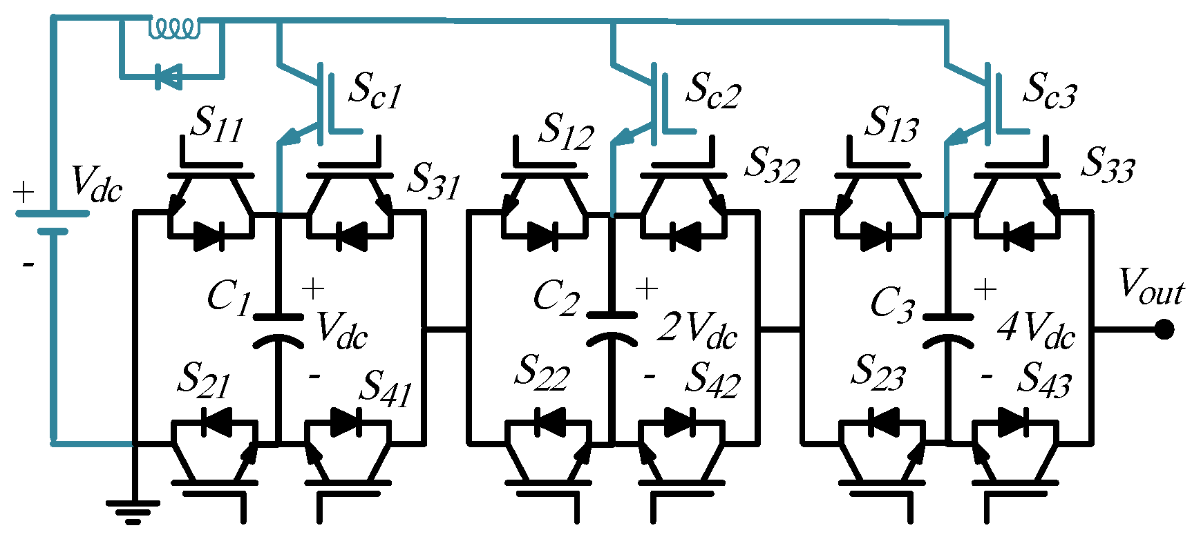
In light of the above, a single-source asymmetric CMI is proposed in this paper, which provides a common ground for ac and dc sides. This topology uses capacitors instead of the isolated dc sources in the HB cells. Each capacitor is independently charged through a charging switch. Since there is a common ground for ac and dc sides, the common mode voltage is zero; hence, this topology can totally eliminate the leakage current in grid-tied PV applications. Another merit of the proposed topology is the capability to boost the input dc voltage; this is also an advantage in many applications such as grid-tied transformerless PV and fuel cell systems. In addition to the mentioned features, the three-phase configuration of the proposed topology draws a continuous input current, which makes it feasible in battery, un-interruptible power supply, and PV applications. The proposed topology can exchange reactive power with the load and the grid as well. Furthermore, it can smoothly charge the capacitors, facilitate the protection, and avoid bulky and expensive transformers in the grid-tied mode. As mentioned, the main issue of the conventional CMI in PV applications is the inter-module leakage currents. However, the proposed topology can address this problem properly and effectively. Compared to the transformer-based single-source multilevel inverters, the proposed topology is smaller in size, lower in cost, and higher in efficiency. Additionally, considering that the SC-based single-source MIs mostly suffer from inrush currents, the proposed topology is, however, an inrush-current free CMI, being a promising converter in many industrial applications.
The rest of the paper is organized as follows: In Section 2, the structure and operation principle of the proposed topology are illustrated. In Section 3, the proposed MI is compared with state-of-the-art MI topology. In Section 4 the performance of the proposed topology in off-grid and grid-tied modes is investigated through simulations. Experimental tests are provided in Section 5, where a fifteen-level 0.55 kVA prototype is adopted to demonstrate the off-grid performance of the proposed topology. Moreover, a seven-level 1.5 kVA prototype is used to extract the grid-tied results. Finally, the overall work is concluded in Section 6.

2. Proposed Topology and Operation Principle

2.1. Conventional CMI in PV Systems

Many solutions are presented in the literature to improve the performance of the CMIs in PV systems. The main problem arises due to the parasitic capacitor in each HB cell that brings inter-module leakage currents [20,21]. These circulating currents cause power loss, EMI, and safety problems [15]. Figure 1a,b shows a grid-tied PV system with a three-cell CMI, and equivalent circuit of the CMV, DMV and leakage currents, respectively.

2.2. General Structure of the Proposed Topology

The proposed topology is synthesized with two parts, namely the main and charging parts. The main part is the conventional asymmetric CMI, in which the isolated dc sources are replaced with capacitors (C1, C2, …, Cn). The charging part is composed of a single dc source (e.g., a PV string, fuel-cell, and batteries), a charging inductor, a freewheeling diode and charging switches (Sc1, Sc2, …, Scn). The general grid-tied configuration of the proposed topology (a configuration with n HB cells) is depicted in Figure 2. Where the main part is colored in black, the charging part is in blue.
As mentioned, the most undesirable phenomenon in an SC-based converter is the inrush currents that emerge in the charging stage of the capacitors. This phenomenon can adversely affect the charging switches and capacitors. In order to limit these currents, a charging inductor (Lch) is connected in series with the dc source, as shown in Figure 2. This inductor can effectively limit the inrush currents. On the contrary, the mentioned inductor can cause voltage spikes and commutation problems in the charging switches. To avoid this and alleviate the EMI, the size of the charging inductor (Lch) can be obtained as
L c h = 1 ( 4 π f ) 2 C n
where f and Cn are the output voltage frequency and equivalent capacitance of the capacitors.
It should be noted that a larger inductor can be used to further reduce the inrush currents. However, this increases the cost and volume of the inverter. A large inductor can also cause overvoltage across the capacitors. To avoid this, as shown in Figure 2, a freewheeling diode (Df) is connected in parallel with the inductor.
In order to illustrate the operation principle of the proposed topology, a fifteen-level configuration, which is depicted in Figure 3, is exemplified. Table 1 shows the switching pattern for each level and different states of the capacitors. It should be mentioned that in Table 1, “on” and “off” states of the switches are indicated by “1” and “0”. The capacitors in the proposed topology experience three states namely the charging, discharging, and floating states. In Table 1, “C”, “D”, and “F” denote the charging, discharging, and floating states of the capacitors. In addition, since the upper switches of the main part (S11, S31, S12, S32, S13, and S33) have complementary states with the lower switches (S21, S41, S22, S42, S23, and S43), only the states of the upper switches are indicated in Table 1 for simplicity.
To clarify, the equivalent circuits of the voltage levels are provided. Due to the page limit, only the positive voltage levels are demonstrated in Figure 4. The negative levels can be found by referring to Table 1. In Figure 4, the charging paths, the capacitors under charge and the load current paths are in red, blue, and dark blue, respectively.

2.3. Three-Phase Configuration

Continuity of the input current in many applications is of high importance. A continuous input current can facilitate the maximum power point tracking (MPPT) process in PV applications and prolong battery life span in storage systems. Referring to Table 1, it can be seen that a single-phase configuration of the proposed topology cannot guarantee a continuous input current because there is no possibility to connect the dc source to any of the capacitors when producing the highest negative voltage level (this is the case for a configuration with any number of voltage-levels). Since the input current is only interrupted in the highest negative voltage level, which is a short interval, this problem will not exist in a three-phase configuration. In such a configuration, when the input current is interrupted in one phase, there are always two paths in the other two phases for the current to flow. Figure 5 depicts the general three-phase configuration of the proposed topology. It is worth mentioning that in the three-phase configuration, the CMV is reduced but not totally eliminated. Thus, in a grid-tied PV application with the three-phase configuration, a limited leakage current is achieved. However, the inter-module leakage currents are totally cancelled out in this configuration.

2.4. Component Design

Referring to Figure 4 and Table 1, it is seen that during one cycle, the lower the dc voltage a HB cell contains, the longer time it resides in the charging mode. For example, as shown in Table 1, the first HB cell, which contains 1 pu voltage, resides in the charging mode for eight times. The number of being in the charging mode for the second and third HB cells is four and two, respectively. Thus, in an l-level structure, the number of being in the charging state for the nth HB cell is calculated as
N c h n = 2 ln ( l + 1 ) l n 2 n
In respect to this, an HB cell with a higher dc voltage will provides the load current for a longer time than others. Therefore, it experiences the highest voltage ripple. The highest voltage ripple of the nth HB cell ( Δ v n ) is given as
{ Δ v n = I m Δ t n C n Δ t n = T ( l N c h n )
where Im, T, and Cn are the maximum value of the load current, time duration of a cycle, and capacitance of the nth capacitor, respectively. This equation can be used to select a proper capacitor for the nth HB cell.
Considering Figure 2, the equivalent circuit of the capacitor experiencing the highest voltage ripple (Cn) is shown in Figure 6. Taking the parameters indicated in Figure 6 into account, the instantaneous voltage in the nth capacitor and the voltage of the mentioned capacitor at the end of a half cycle are, respectively, given as
v c n ( t ) = ( 2 n 1 ) v d c t R C n
v c n ( T d ) = ( 2 n 1 ) v d c T d R C n
The maximum voltage ripple in the nth capacitor can be given as
Δ v c n = f T d ( ( 2 n 1 ) v d c v c n ( T d ) ) = f T d ( 2 n 1 ) v d c ( 1 e T d R C n )
As it is an asymmetric topology, the HB cells in the proposed topology include different dc voltage values. Considering vdc as the input voltage, the voltage across the nth cell is given as
V c n = 2 n 1 v d c
The voltage stress on the main and charging switches in the nth HB cell is equal to the voltage of capacitor in that HB cell.
The peak output voltage of an n-cell configuration is given as
v m = v d c k = 1 n 2 k 1
The number of switches of an l-level configuration of the proposed and conventional asymmetric CMI topologies is, respectively, indicated as
N s w P 5 ln ( l + 1 2 ) l n 2
N s w C 4 ln ( l + 1 2 ) l n 2
This implies that the proposed topology requires one extra switch in each cell (one charging switch for each cell).
The total voltage stresses of the switches in the proposed and the conventional asymmetric CMI topologies are, respectively, indicated as
T V S p = 5 v d c N s w P k = 1 N s w p / 5 2 k 1
T V S c = 4 v d c N s w c k = 1 N s w c / 4 2 k 1
Implying that the voltage stresses of the switches in both topologies are the same.

3. Benchmarking with Prior-Art Inverters

Several efforts have been done to make the CMI compatible with grid-tied PV applications [22,23,24,25,26,27,28,29]. The main difficulties with the CMI in PV applications are the leakage current and complicated MPPT [14]. Single-source CMIs facilitate the MPPT, but the leakage current problem remains. A transformer can solve the problem, however, transformers are not recommended in grid-tied PV applications due to extra power losses and additional costs. Therefore, as stated previously, the SC-based CMI can fulfill many requirements. The state-of-the-art PV MI topologies are compared with the proposed MI topology in this section to assess its pros and cons. Table 2 lists the main features of the considered MI topologies.
In table, Nsw, Nd, Nc, G, and TSV are the number of switches, diodes, capacitors, voltage gain, and the total standing voltage of the switches. The TSV is calculated as
T S V = n = 0 n = k V s w n + n = 0 n = k V s d n V o u t
The proposed topology and the topology in [29] can be scaled up to obtain higher voltage gains and levels. However, this is not the case for the other topologies. Since the proposed MI topology is a common-ground-type inverter and the topology in [24] is a mid-point-grounded topology, these two topologies can limit the leakage current in grid-tied PV applications. In this regard, the other topologies listed in Table 2 encounter serious problems. The main disadvantage of the MI topologies in [24] and [25] is that they require a complicated control approach to balance the voltages across the capacitors. The voltage balancing system of these topologies should sense the direction of the ac current and the capacitor voltage magnitude, and then the sensed values are processed though the processor to execute the right switching pattern to balance the voltage of the capacitors. However, this does not happen in the other topologies and the proposed one. Notably, the topologies in [23,25,27,28] suffer from high inrush currents in the charging stage of the capacitor. Owing to the controlled voltage balancing of the capacitors, the inrush current does not appear in the topologies in [24,25]. In the proposed topology and the topology in [29], the inrush current is limited through the charging inductor. As it is seen in Table 2, the proposed inverter has a fairly low TSV, high voltage gain and fewer components.

4. Simulation Results

In order to verify the performance of the proposed topology, both the single-phase and three-phase configurations are simulated under MATLAB/Simulink. The main parts in the considered configurations are assumed to be a fifteen-level CMI. The simulated models are tested under off-grid and grid-tied modes. In the off-grid mode, a general dc source supplies the load through the proposed topology.

4.1. Off-Grid Mode

As illustrated earlier, the three-phase and single-phase configurations only differ in the input current shapes. For this reason, mostly the single-phase configuration is investigated. Table 3 shows the characteristics of the utilized components in the off-grid mode. Figure 7a shows the output and capacitor voltages under no-load condition. A fast Fourier transform (FFT) analysis of the output voltage is depicted in Figure 7b.
Furthermore, the output voltage, load current, and capacitor voltages, when supplying a purely resistive load of 0.55 kW, are shown in Figure 8a. As seen in Figure 8a, under this condition, the voltage across the capacitors is properly balanced through the charging circuit. Additionally, the capacitor currents along with the input current under the studied loading condition are shown in Figure 8b. It can be seen that the charging unit can properly limit the inrush current of the capacitors. However, the main demerit of the charging process is the discontinuity of the input current due to the absence of a path for the input current when developing the highest negative voltage level.
In order to demonstrate the ability of the proposed topology to provide reactive power, a resistive-inductive load of 0.5 kW + 0.35 kVar is connected. Figure 9a shows the output voltage and load current under the mentioned condition. As shown in Figure 9a, the proposed topology can satisfactorily supply the reactive power. Additionally, the voltage stress and current of the charging switches are shown in Figure 9b. According to Figure 9b, it is known that the charging switch in the last cells can tolerate the highest voltage stress.
As mentioned previously, a three-phase configuration of the proposed topology draws a continuous current from the input side. This is proven by considering a three-phase fifteen-level configuration, which supplies a balanced three-phase load under three loading cases (3.8 kW, 4.8 kW + 1.2 kVar, 3 kW + 1.2 kVar). The input current of the phases and the total input current under the mentioned loading condition are shown in Figure 10a. As it is seen in Figure 10a, the input current is a continuous current. Moreover, the output voltages together with the load current under the mentioned condition are shown in Figure 10b,c, respectively. When the freewheeling diode is removed, the capacitors are exposed to overvoltage at the initial instance. Soft starting strategies can be employed to avoid the overvoltage of the capacitors.

4.2. Grid-Tied Mode

Similar to the off-grid mode, a fifteen-level configuration of the proposed topology is used to deliver the desired powers to the grid. To this end, the ac components are transferred to the dq0 frame and two proportional-integral (PI) controllers are employed to control the active and reactive powers. Table 4 shows the characteristics of the considered system.
The simulation results of the single-phase grid-connected model are shown in Figure 11. The desired (reference) and delivered active power to the grid is shown in Figure 11a. The reference of the active power can be obtained by the MPPT system in PV applications. The reference and developed reactive powers are exhibited in Figure 11b. As shown in Figure 11b, the proposed topology has succeeded to provide a bidirectional reactive power flow. The input current is depicted in Figure 11c. The output voltage of the inverter along with the injected current is exhibited in Figure 11d.
It should be pointed out that one of the significant features of the proposed MI topology is its ability to eliminate the leakage current in grid-tied PV systems without using any additional components.
Furthermore, the simulation results of a grid-connected three-phase model are demonstrated in Figure 12. The injected active and reactive powers to the grid are depicted in Figure 12a,b. As seen in Figure 12, the proposed MI has deservedly developed the desired powers.
As discussed previously, the three-phase configuration of the proposed topology draws a continuous current from the dc-link. Figure 13a shows the input current and proves this. In order to investigate the leakage current, a parasitic capacitor of 200 nF is considered between the negative pole of the dc-side and ac-ground, Figure 13b shows the leakage current. As shown in Figure 13b, the root mean square (RMS) value of the leakage current is in the acceptable range. However, it is possible to reduce this through the proper control and/or switching approaches. It is worth mentioning that since the proposed topology does not use PV modules inside the H-bridge cells, there are no inter-module leakage currents.
Furthermore the output voltage and the injected current are shown in Figure 14. It is to be noted that this paper is not aimed at designing a proper control system. It is possible to obtain a more accurate result through a precise control approach.

5. Experimental Results

5.1. Off-Gird Results

In order to validate the feasibility of the proposed topology, a laboratory-scale prototype is tested. Figure 15 depicts the employed prototype and Table 5 lists the utilized components. It should be noted that the level-shifted SPWM strategy is adopted to compute the switching signals.
Figure 16 exhibits the output voltage under the no-load condition and the FFT analysis of the voltage. As can be seen, the harmonics around the fundamental frequency have negligible magnitude, while the harmonics around the multiples of the switching frequency are of high amplitude. Since these harmonics are far away from the fundamental frequency, they can easily be eliminated using small filters.
The output voltage along with the load current, when the prototype supplies a purely resistive load of 550 W is shown in Figure 17a. In order to assess the voltage ripple of the capacitors, the ac components of the capacitor voltages are shown in Figure 17b–d. Additionally, the charging current of the capacitor under 550 W load is shown in Figure 17e. As it is seen, there is no sharp spike on the charging current of the capacitors, which implies that the charging inductor smoothen the charging currents.
In order to prove the capability of the proposed topology to provide reactive power, a resistive-inductive load of 500 W + 350 Var is then considered. Figure 18 exhibits the output voltage and load current under this condition. As can be seen, the proposed topology can supply the reactive power without any constraints.

5.2. Grid-Tied Results

In order to extract the grid-tied results a seven-level prototype with two cells is employed. The characteristic of the prototype and grid is listed in Table 6. In this test the sample based current control is used to inject the desired active and reactive powers to the grid.
Three scenarios are considered in grid-tied test. In the first scenario a pure active power of 1.5 kW is injected to the grid. The injected current and grid voltage under this condition are shown in Figure 19a. The FFT analysis of the injected current under the mentioned condition is shown in Figure 19b. Furthermore, the output voltage of the inverter along with the provided current is shown in Figure 19c.
In the second scenario the active power of 1.2 kW and reactive power of 0.9 kVar is injected to the grid and in the third scenario the active power of 1.2 kW is injected to the grid and reactive power of 0.9 kVar absorbed from the grid. The grid voltage together with the injected current to the grid is shown in Figure 20a,b.
The seven-level prototype for grid-tied application is exhibited in Figure 21.

6. Conclusions

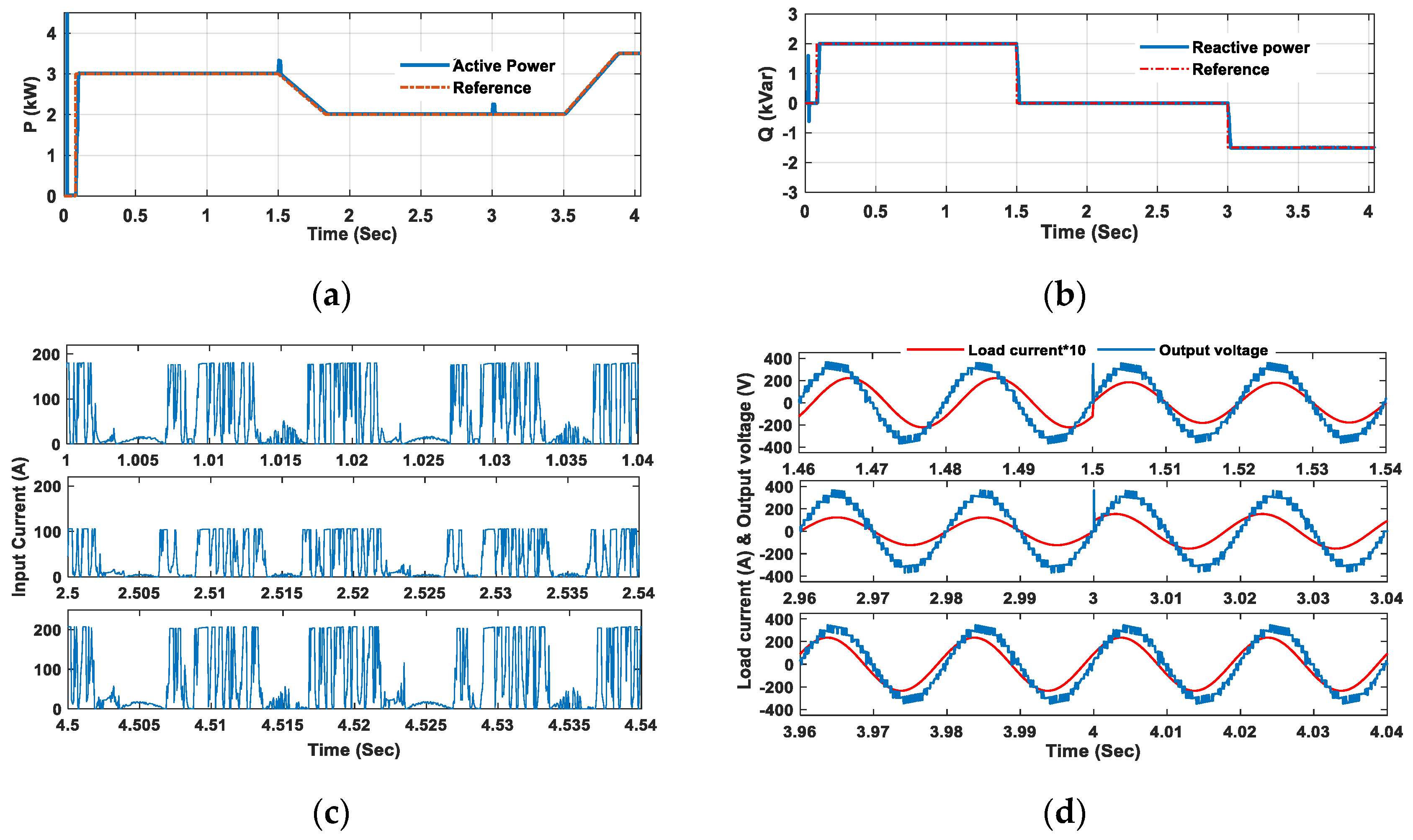
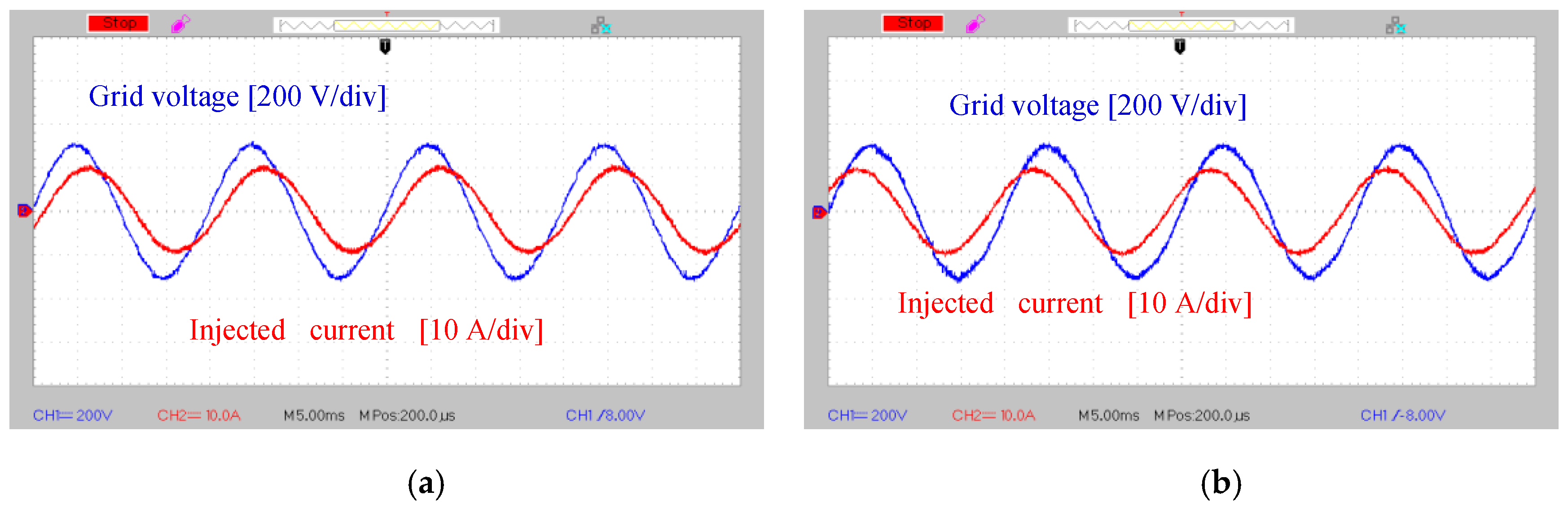
In this paper, a single-source high step-up asymmetric power converter topology is proposed. The proposed topology offers several advantages in many industrial applications such as PV, fuel cell, etc. It is synthesized with two parts, namely, the main and charging parts. The main part is the same as the conventional asymmetric CMI with certain capacitors instead of the isolated dc sources. The charging part, however, consists of charging switches, a charging inductor, a freewheeling diode, and one dc source. The main feature of the proposed topology is to provide a common-ground for ac and dc sides, which eliminates the leakage current in grid-tied PV applications. It also has the ability to boost the input voltage. Thus, in the grid-tied PV applications, bulky and expensive transformers can be avoided. Moreover, it uses only one dc source, at the expense of using many switches, employing many switches can be considered as the main drawback of the proposed inverter. Simulations and experiments were performed to verify the effectiveness of the proposed topology. Through simulations, the performances of the suggested topology with single- and three-phase configuration, in both off-grid and grid-tied conditions, were assessed. In the experimental tests, the performance of the proposed topology was studied in the presence of a 550-VA load. Moreover, using a 1.5 kVA seven-level prototype the grid-tied results were provided. Both results have demonstrated the feasibility of the proposed multilevel inverter in terms of the ability to develop a boosted voltage of high quality using only one dc source.

Author Contributions

The concept, theoretical analysis, and preparation of the manuscript were with H.K.J. N.V.K. contributed to extract the grid-tied experimental results. M.A., K.Z. and S.H.H. were supervisors and helped to investigate and assess the performance of the proposed inverter topology. Y.Y. and F.B. supervised the work, helped to extract experimental results, edited the manuscript, and provided financial supports. All authors have read and agreed to the published version of the manuscript.

Funding

This work was supported under the research project—Reliable Power Electronic based Power Systems (REPEPS) by The Velux Foundations under Award No.: 00016591.

Conflicts of Interest

The authors declare no conflict of interest.

References

  1. Wu, F.; Li, X.; Feng, F.; Gooi, H.B. Modified cascaded multilevel grid-connected inverter to enhance European efficiency and several extended topologies. IEEE Trans. Ind. Inform. 2015, 11, 1358–1365. [Google Scholar] [CrossRef]
  2. Sepahvand, H.; Liao, J.; Ferdowsi, M.; Corzine, K.A. Capacitor voltage regulation in single-DC-source cascaded H-bridge multilevel converters using phase-shift modulation. IEEE Trans. Ind. Electron. 2013, 60, 3619–3626. [Google Scholar] [CrossRef]
  3. Banaei, M.R.; Jahan, H.K.; Salary, E. Single-source cascaded transformers multilevel inverter with reduced number of switches. IET Power Electron. 2012, 5, 1748–1753. [Google Scholar] [CrossRef]
  4. Vazquez, S.; Leon, J.I.; Franquelo, L.G.; Padilla, J.J.; Carrasco, J.M. DC-voltage-ratio control strategy for multilevel cascaded converters fed with a single DC source. IEEE Trans. Ind. Electron. 2009, 56, 2513–2521. [Google Scholar] [CrossRef]
  5. Taghvaie, A.; Adabi, J.; Rezanejad, M. A multilevel inverter structure based on a combination of switched-capacitors and DC sources. IEEE Trans. Ind. Inform. 2017, 13, 2162–2171. [Google Scholar] [CrossRef]
  6. Jahan, H.K.; Zare, K.; Abapour, M. Verification of a low components nine-level cascaded-transformer multilevel inverter in grid-tied mode. IEEE J. Emerg. Sele. Topi. Power Electron. 2018, 6, 429–440. [Google Scholar] [CrossRef]
  7. Song, S.G.; Kang, F.S.; Park, S.J. Cascaded multilevel inverter employing three-phase transformers and single DC input. IEEE Trans. Ind. Electron. 2009, 56, 2005–2014. [Google Scholar] [CrossRef]
  8. Jahan, H.K.; Naseri, M.; Haji-Esmaeili, M.M.; Abapour, M.; Zare, K. Low component merged cells cascaded-transformer multilevel inverter featuring an enhanced reliability. IET Power Electron. 2017, 10, 855–862. [Google Scholar] [CrossRef] [Green Version]
  9. Panda, A.K.; Suresh, Y. Performance of cascaded multilevel inverter by employing single and three-phase transformers. IET Power Electron. 2012, 5, 1694–1705. [Google Scholar] [CrossRef]
  10. Pereda, J.; Dixon, J. High-frequency link: A solution for using only one dc source in asymmetric cascaded multilevel inverters. IEEE Trans. Ind. Electron. 2011, 58, 3884–3892. [Google Scholar] [CrossRef]
  11. Wang, L.; Zhang, D.; Wang, Y.; Wu, B.; Athab, H.S. Power and voltage balance control of a novel three-phase solid-state transformer using multilevel cascaded H-bridge inverters for microgrid applications. IEEE Trans. Power Electron. 2016, 31, 3289–3301. [Google Scholar] [CrossRef]
  12. Barzegarkhoo, R.; Kojabadi, H.M.; Zamiry, E.; Vosough, N.; Chang, L. Generalized structure for a single phase switched-capacitor multilevel inverter using a new multiple DC link producer with reduced number of switches. IEEE Trans. Power Electron. 2016, 31, 5604–5617. [Google Scholar] [CrossRef]
  13. Du, Z.; Ozpineci, B.; Tolbert, L.M.; Chiasson, J.N. DC–AC Cascaded H-bridge multilevel boost inverter with no inductors for electric/hybrid electric vehicle applications. IEEE Trans. Ind. Appl. 2009, 45, 963–970. [Google Scholar] [CrossRef]
  14. Villanueva, E.; Correa, P.; Rodriguez, J.; Pacas, M. Control of a single-phase cascaded H-bridge multilevel inverter for grid-connected photovoltaic systems. IEEE Trans. Ind. Electron. 2009, 56, 4399–4406. [Google Scholar] [CrossRef]
  15. Zhou, Y.; Li, H. Analysis and suppression of leakage current in cascaded-multilevel-inverter-based PV systems. IEEE Trans. Power Electron. 2014, 29, 5265–5277. [Google Scholar] [CrossRef]
  16. Kadam, A.; Shukla, A. A multilevel transformerless inverter employing ground connection between PV negative terminal and grid neutral point. IEEE Trans. Ind. Electron. 2017, 64, 8897–8907. [Google Scholar] [CrossRef]
  17. Siwakoti, Y.P.; Blaabjerg, F. A single-phase transformerless inverter with charge pump circuit concept for grid-tied PV applications. IEEE Trans. Ind. Electron. 2018, 65, 2100–2111. [Google Scholar] [CrossRef]
  18. Anurag, A.; Deshmukh, N.; Maguluri, A.; Anand, S. Integrated DC–DC Converter Based Grid-Connected Transformerless Photovoltaic Inverter with Extended Input Voltage Range. IEEE Trans. Power Electron. 2018, 33, 8322–8330. [Google Scholar] [CrossRef]
  19. Khan, M.N.H.; Forouzesh, M.; Siwakoti, Y.P.; Li, L.; Kerekes, T.; Blaabjerg, F. Transformerless Inverter Topologies for Single-Phase Photovoltaic Systems: A Comparative Review. IEEE J. Emerg. Sele. Topi. Power Electron. 2019, 65, 805–835. [Google Scholar] [CrossRef]
  20. Kumar, V.V.S.P.; Fernandes, B.G. Minimization of inter-module leakage current in cascaded H-bridge multilevel inverters for grid connected solar PV applications. Proc. IEEE Appl. Power Electron. Conf. Expo. 2016, 2673–2678. [Google Scholar] [CrossRef]
  21. Wang, F.; Li, Z.; Do, H.T.; Zhang, D. A modified phase disposition pulse width modulation to suppress the leakage current for the transformerless cascaded H-bridge inverters. IEEE Trans. Ind. Electron. 2018, 65, 1281–1289. [Google Scholar] [CrossRef]
  22. Sun, X.; Wang, B.; Zhou, Y.; Wang, W.; Du, H.; Lu, Z. A Single DC Source Cascaded Seven-Level Inverter Integrating Switched-Capacitor Techniques. IEEE Trans. Ind. Electron. 2016, 63, 7184–7194. [Google Scholar] [CrossRef]
  23. Lee, S.S. Single-Stage Switched-Capacitor Module (S3CM) Topology for Cascaded Multilevel Inverter. IEEE Trans. Power Electron. 2018, 33, 8204–8207. [Google Scholar] [CrossRef] [Green Version]
  24. Phanikumar, C.; Roy, J.; Agarwal, V. A Hybrid Nine-Level, 1-φ Grid Connected Multilevel Inverter with Low Switch Count and Innovative Voltage Regulation Techniques across Auxiliary Capacitor. IEEE Trans. Power Electron. 2019, 34, 2159–2170. [Google Scholar] [CrossRef]
  25. Liu, J.; Lin, W.; Wu, J.; Zeng, J. A Novel Nine-Level Quadruple Boost Inverter with Inductive-Load Ability. IEEE Trans. Power Electron. 2019, 34, 4014–4018. [Google Scholar] [CrossRef]
  26. Sandeep, N.; Yaragatti, U.R. Operation and Control of an Improved Hybrid Nine-Level Inverter. IEEE Trans. Ind. Appl. 2017, 53, 5676–5686. [Google Scholar] [CrossRef]
  27. Siddique, M.D.; Mekhilef, S.; Shah, N.M.; Sandeep, N.; Ali, J.S.M.; Iqbal, A.; Ahmed, M.; Ghoneim, S.S.; Al-Harthi, M.M.; Alamri, B.; et al. A Single DC Source Nine-Level Switched-Capacitor Boost Inverter Topology with Reduced Switch Count. IEEE Access 2020, 8, 5840–5851. [Google Scholar] [CrossRef]
  28. Siddique, M.D.; Mekhilef, S.; Shah, N.M.; Ali, J.S.M.; Meraj, M.; Iqbal, A.; Al-Hitmi, M.A. A New Single Phase Single Switched-Capacitor Based Nine-Level Boost Inverter Topology with Reduced Switch Count and Voltage Stress. IEEE Access 2019, 7, 174178–174188. [Google Scholar] [CrossRef]
  29. Jahan, H.K.; Abapour, M.; Zare, K.; Hosseini, S.H.; Blaabjerg, F.; Yang, Y. A Multilevel Inverter with Minimized Components Featuring Self-balancing and Boosting Capabilities for PV Applications. IEEE J. Emerg. Sel. Top. Power Electron. 2019. [Google Scholar] [CrossRef]
Figure 1. Conventional cascaded multilevel inverter (CMI)-based PV system: (a) a three-cell grid-tied CMI; (b) equivalent circuit to illustrate the common mode voltage (CMV), differential-mode voltage (DMV) and inter-module currents.
Mathematics 08 01716 g001
Figure 2. General configuration of the proposed topology in grid-tied PV applications.
Mathematics 08 01716 g002
Figure 3. A fifteen-level configuration of the proposed topology.
Mathematics 08 01716 g003
Figure 4. Charging and load current paths: (ah) zero to seventh voltage-levels of the topology in Figure 3, respectively, where the PV module is replaced with a dc source for clarity.
Mathematics 08 01716 g004
Figure 5. General three-phase configuration of the proposed topology.
Mathematics 08 01716 g005
Figure 6. Equivalent circuit and discharging diagram of a capacitor in an HB cell.
Mathematics 08 01716 g006
Figure 7. Simulation results of the single-phase configuration in the off-grid mode (no-load condition): (a) capacitor and output voltages; (b) fast Fourier transform (FFT) analysis of the output voltage.
Mathematics 08 01716 g007
Figure 8. Simulation results of the single-phase configuration in the off-grid mode (under a purely resistive loading condition): (a) load current along with the capacitor and output voltages; (b) capacitor and input currents.
Mathematics 08 01716 g008
Figure 9. Simulation results of the single-phase configuration in the off-grid mode (under a resistive-inductive loading condition): (a) load current and output voltage; (b) voltage stress and current of the charging switches.
Mathematics 08 01716 g009
Figure 10. Simulation results of the three-phase configuration in the off-grid mode: (a) input current of the phase and total input current; (b) load current; (c) output voltage.
Mathematics 08 01716 g010
Figure 11. Simulation results of the single-phase grid-connected model: (a) the developed and reference of the active power; (b) the developed and reference of the active power; (c) input current; (d) output voltage and load current.
Mathematics 08 01716 g011
Figure 12. Simulation results of the active and reactive power of the three-phase grid-connected model: (a) the injected active power to the grid; (b) the injected reactive power to the grid.
Mathematics 08 01716 g012
Figure 13. Simulation results of input and leakage current of the three-phase grid-connected model: (a) input current; (b) leakage current.
Mathematics 08 01716 g013
Figure 14. Simulation results of the output voltage and injected current of the three-phase grid-connected model.
Mathematics 08 01716 g014
Figure 15. Experimental setup of the proposed topology (15-level).
Mathematics 08 01716 g015
Figure 16. Measured output voltage of the proposed single-phase configuration (15-level) under no-load condition and its FFT analysis.
Mathematics 08 01716 g016
Figure 17. Experimental results under a purely resistive loading condition: (a) output voltage and load current under the purely resistive loading condition; (b,c), and (d) ac components of the capacitor voltages; (e) input current and charging current of the capacitors.
Mathematics 08 01716 g017aMathematics 08 01716 g017b
Figure 18. Output voltage and load current under the inductive-resistive loading condition.
Mathematics 08 01716 g018
Figure 19. Grid-tied results of the active power: (a) grid voltage and injected current; (b) FFT analysis of the injected current; (c) output voltage and current of the prototype.
Mathematics 08 01716 g019
Figure 20. Grid-tied results of the injected current: (a) the output voltage and load current when injecting the active and reactive current to the grid; (b) grid-voltage and injected current when injecting the active power and absorbing the reactive power.
Mathematics 08 01716 g020
Figure 21. Seven-level setup for grid-tied application.
Mathematics 08 01716 g021
Table 1. Operation states of components shown in Figure 3.
LevelsMain SwitchesCharging SwitchesCapacitorsVout
S11, S31, S12S32S13, S33Sc1, Sc2,Sc2C1, C2, C3
7010101100C,D,D7Vdc
6000101100C,D,D6Vdc
5100101010D,C,D5Vdc
4000001100C,D,D4Vdc
3100001010D,C,D3Vdc
2001001100C,D,D2Vdc
1101001001D,DC1Vdc
0000000100C,F,F0
−1100000010D,C,D−1Vdc
−2001000100C,D,D−2Vdc
−3101000001D,D,C−3Vdc
−4000010100C,F,D−4Vdc
−5100010010D,C,D−5Vdc
−6001010100C,D,D−6Vdc
−7101010000D,D,D−7Vdc
Table 2. Comparison.
TopologyNswNdNcGTSVCoupled InductorLeakage Current Limiting
[22]140234.67nono
[23]12-225.5nono
[24]10-20.58yesyes
[25]83345.75nono
[26]12-345.25nono
[27]9-225.5nono
[28]11-325nono
[29]84426nono
[Proposed]100235noyes
Table 3. Components of the off-grid model.
ComponentValueComponentValue
Vdc46 VLch (3ϕ)0.5 mH
Power rating550 WC1, C2, C33300 µF
Lch (ϕ)1.8 mHfsw5 kHz
Reference voltage311 V (peak), 50 Hz
Table 4. Component of the grid-connected model.
Ki42.3Grid-side filter2.8 mH + 30 mΩ
Kp700fsw5 kHz
V g max 320 VLch1.8 mH
f50 HzC1, C2, C33300 µF
Table 5. Electrical parameters and component specifications.
ComponentSpecificationElectrical ParameterValue
Main SwitchesIRFP350Resistive load550 W
Charging switchesIRFP460RL load650 VA
Opto-couplerTLP250Vout(RMS)220 v, 50 Hz
Capacitors3300 µFVdc47 V
Lch2.8 mHfsw5 kHz
DiodesFFPF20UP40S# of HB cells3 (15-level)
Table 6. Component of the grid-connected model.
Main SwitchesFQA14N30Grid-side filter1.73 mH
Charging switchesSTP30NM30NSwitching frequency (fsw)22 kHz
RMS grid voltage220 VLch1.6 mH
Grid frequency (f)50 HzC1, C23300 µF

