Advances on Sensors Based on Carbon Nanotubes


Abstract
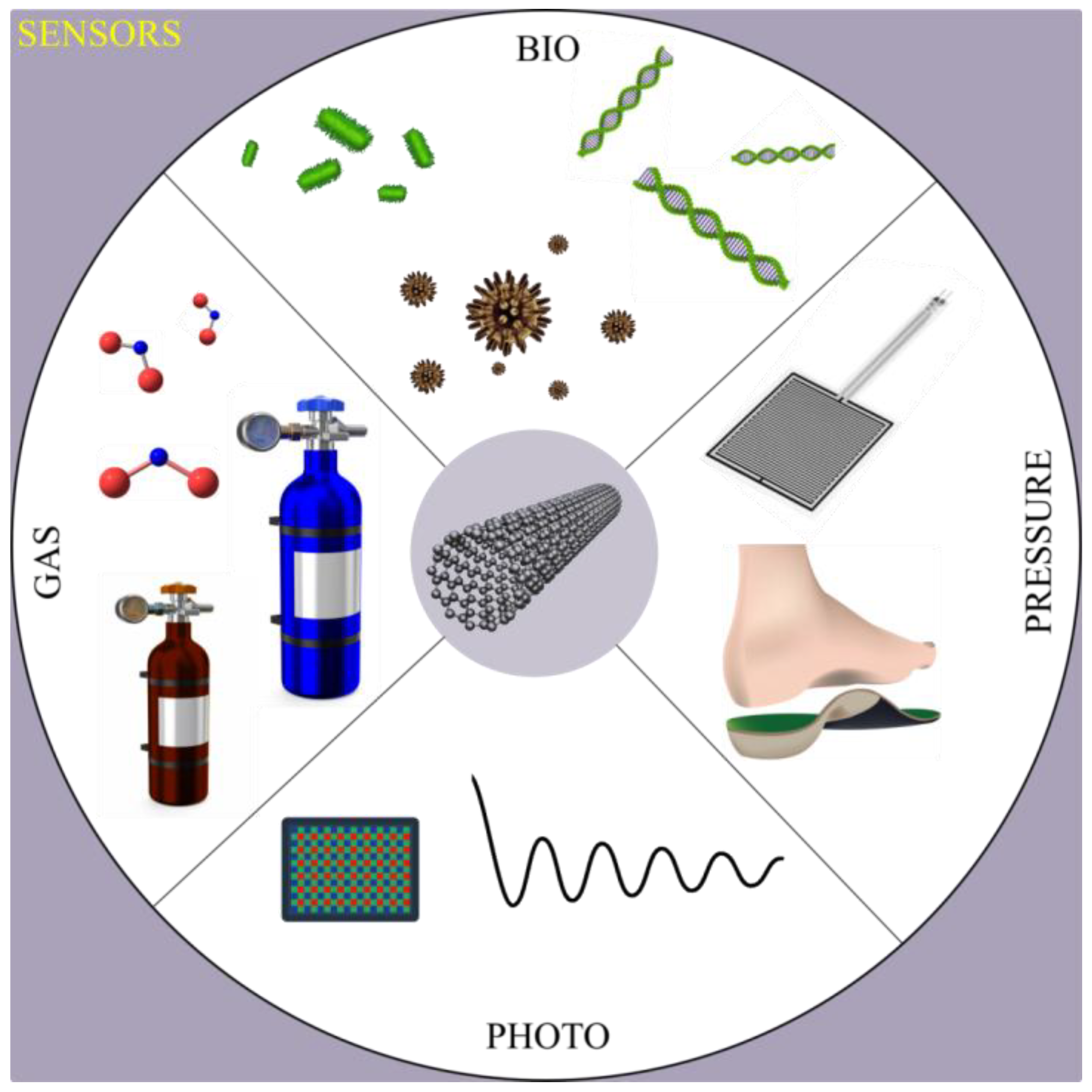
1. Introduction
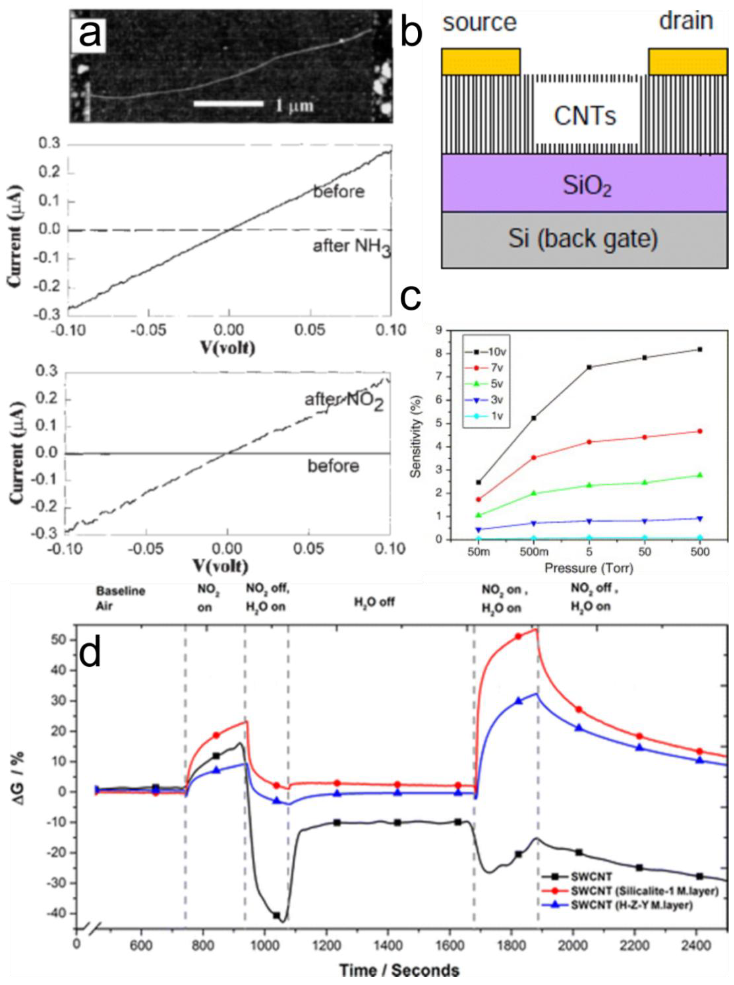
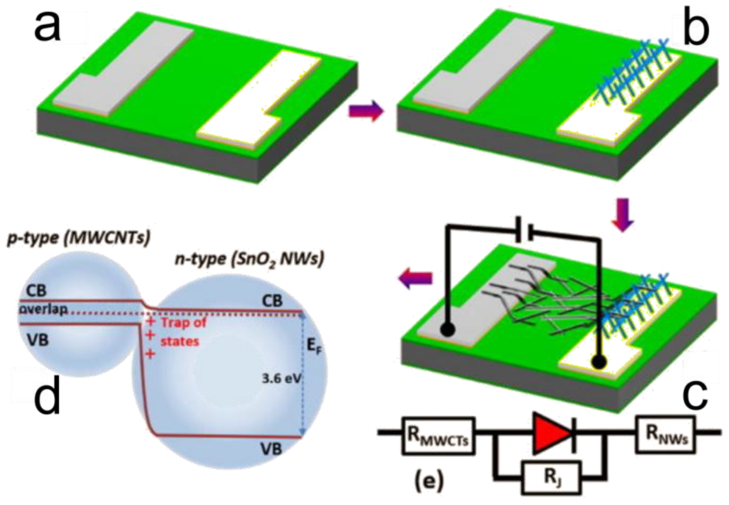
2. Carbon Nanotube-Based Gas Sensors
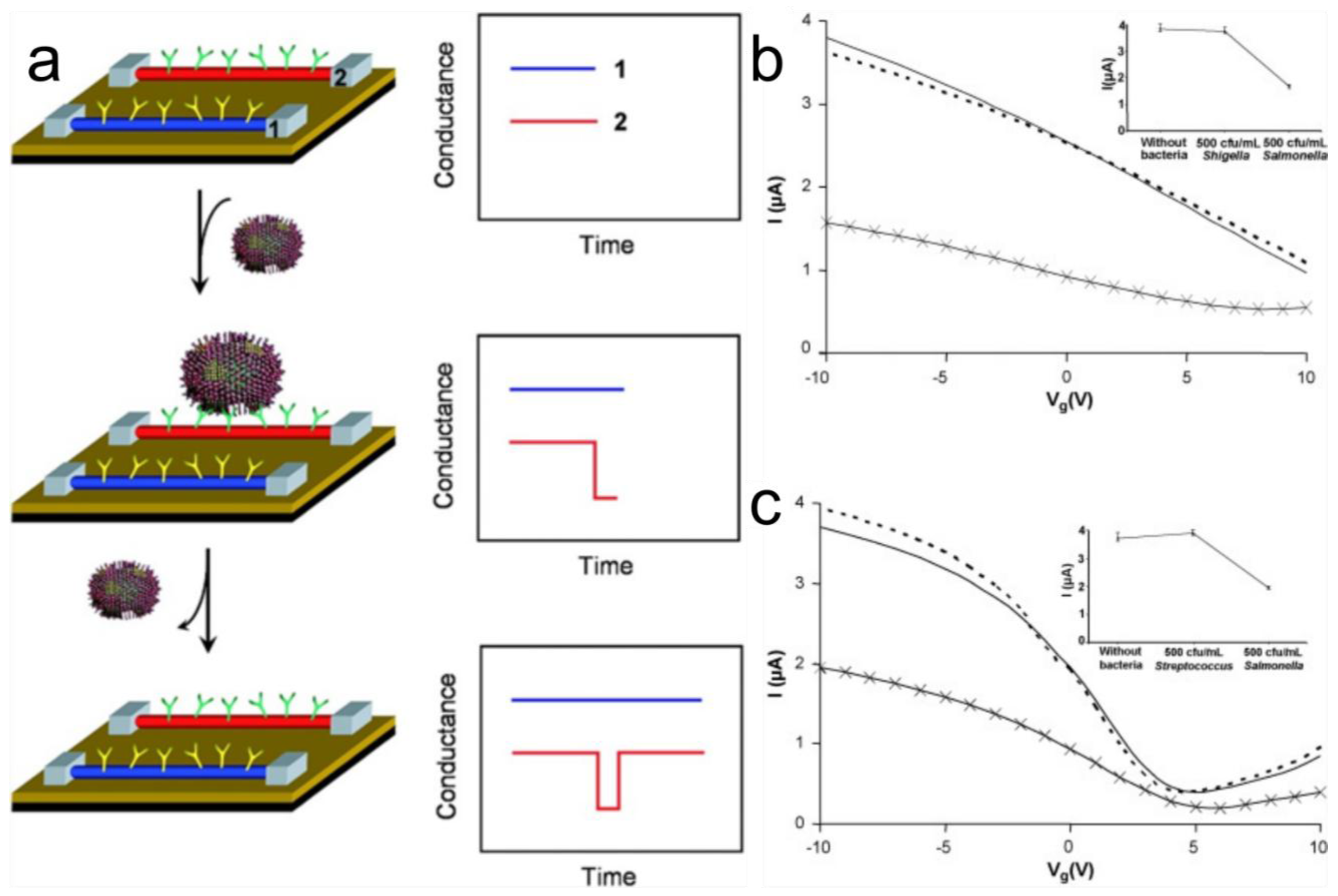
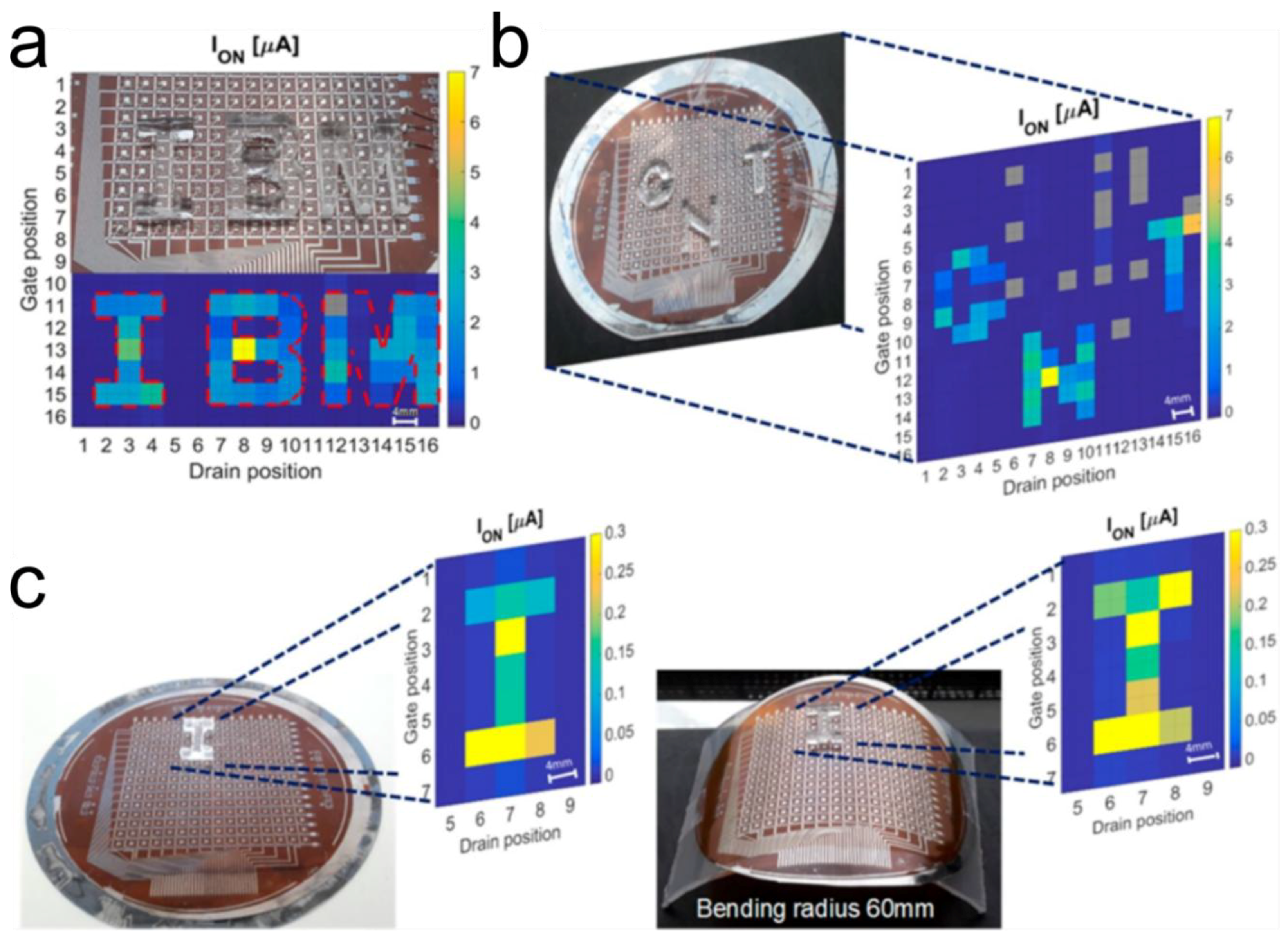
3. Carbon Nanotube-Based Biosensors with FET Configuration
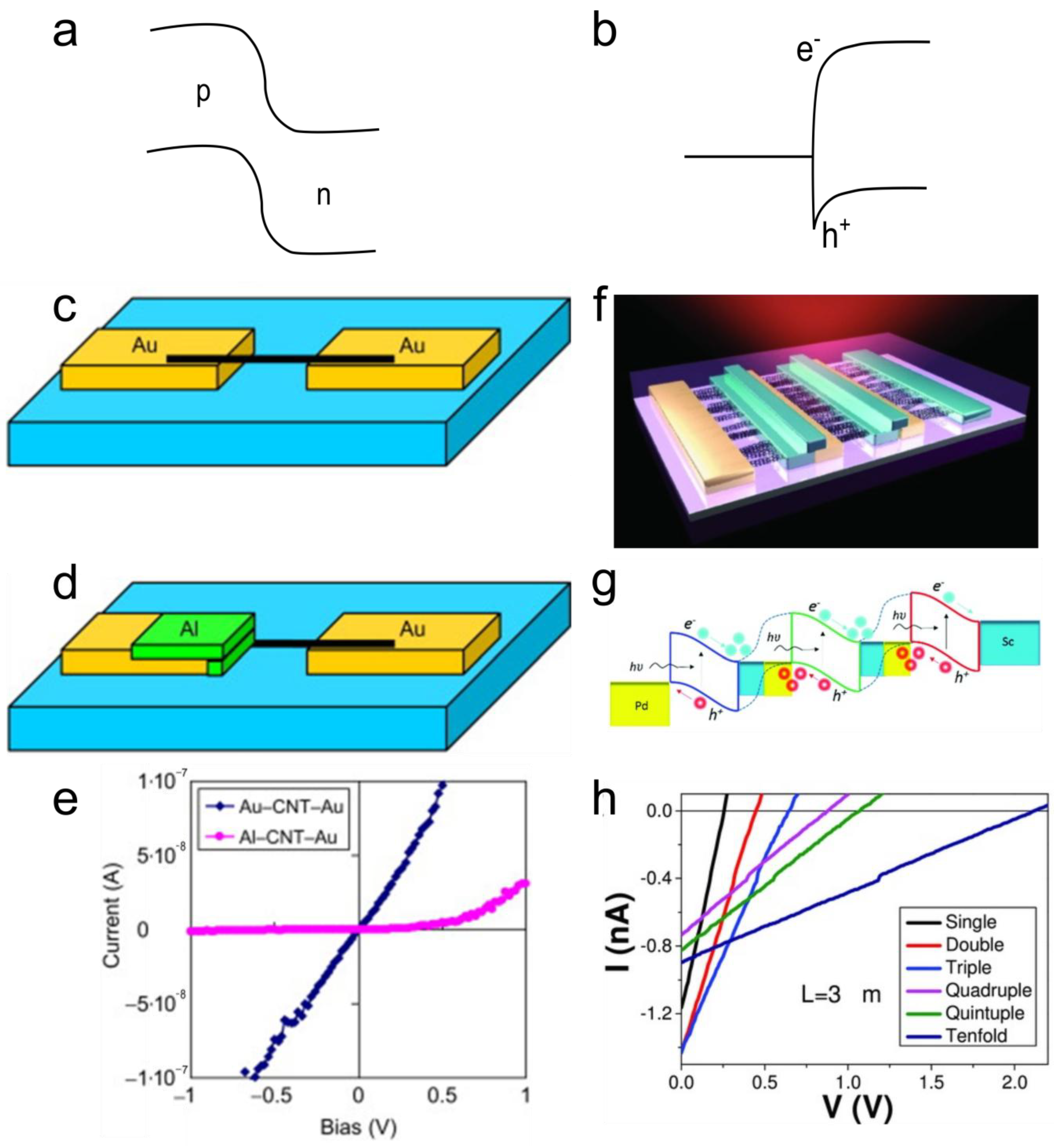
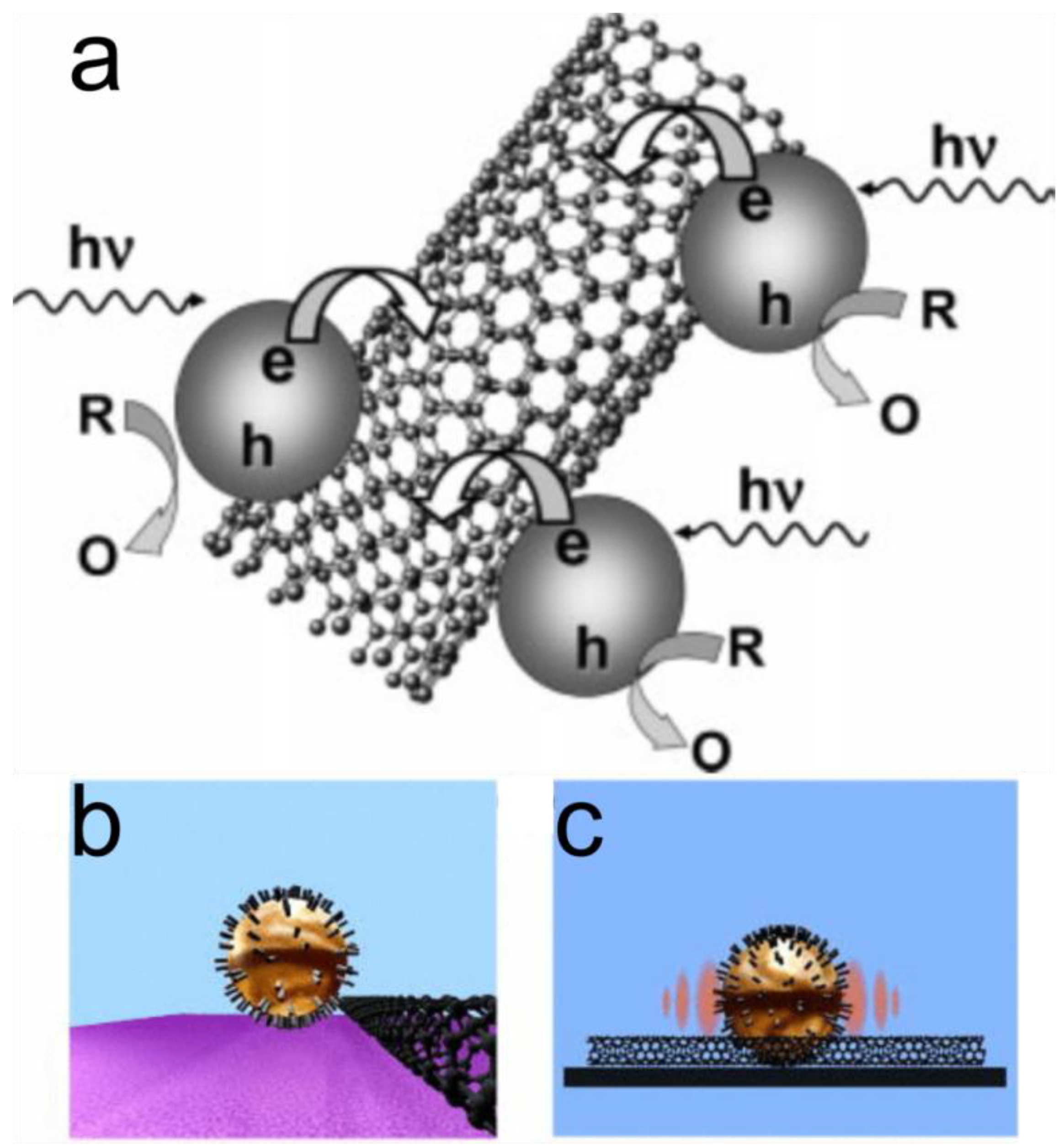
4. Carbon Nanotube-Based Photo-Sensors
5. Carbon Nanotube-Based Pressure Sensors
6. Conclusions, Challenges and Future Perspectives
Author Contributions
Funding
Conflicts of Interest
References
- Iijima, S. Helical microtubules of graphitic carbon. Nature 1991, 354, 56–58. [Google Scholar] [CrossRef]
- Saito, R.; Dresselhaus, G.; Dresselhaus, M.S. Physical Properties of Carbon Nanotubes; World Scientific: Singapore, 1998. [Google Scholar]
- Georgakilas, V.; Kordatos, K.; Prato, M.; Guldi, D.M.; Holzinger, M.; Hirsch, A. Organic functionalization of carbon nanotubes. J. Am. Chem. Soc. 2002, 124, 760–761. [Google Scholar] [CrossRef] [PubMed]
- Balasubramanian, K.; Burghard, M. Chemically functionalized carbon nanotubes. Small 2005, 1, 180–192. [Google Scholar] [CrossRef] [PubMed]
- Holzinger, M.; Vostrowsky, O.; Hirsch, A.; Hennrich, F.; Kappes, M.; Weiss, R.; Jellen, F. Sidewall functionalization of carbon nanotubes. Angew. Chem. Int. Ed. 2001, 40, 4002–4005. [Google Scholar] [CrossRef]
- Hirsch, A. Functionalization of single-walled carbon nanotubes. Angew. Chem. Int. Ed. 2002, 41, 1853–1859. [Google Scholar] [CrossRef]
- Dyke, C.A.; Tour, J.M. Covalent functionalization of single-walled carbon nanotubes for materials applications. J. Phys. Chem. A 2004, 108, 11151–11159. [Google Scholar] [CrossRef]
- Robel, I.; Bunker, B.A.; Kamat, P.V. Single-Walled Carbon Nanotube–CdS Nanocomposites as Light-Harvesting Assemblies: Photoinduced Charge-Transfer Interactions. Adv. Mater. 2005, 17, 2458–2463. [Google Scholar] [CrossRef]
- Scarselli, M.; Camilli, L.; Castrucci, P.; Nanni, F.; Del Gobbo, S.; Gautron, E.; Lefrant, S.; De Crescenzi, M. In situ formation of noble metal nanoparticles on multiwalled carbon nanotubes and its implication in metal–nanotube interactions. Carbon 2012, 50, 875–884. [Google Scholar] [CrossRef]
- Ren, G.; Xing, Y. Deposition of metallic nanoparticles on carbon nanotubes via a fast evaporation process. Nanotechnology 2006, 17, 5596. [Google Scholar] [CrossRef]
- Scarselli, M.; Castrucci, P.; Camilli, L.; Del Gobbo, S.; Casciardi, S.; Tombolini, F.; Gatto, E.; Venanzi, M.; De Crescenzi, M. Influence of Cu nanoparticle size on the photo-electrochemical response from Cu–multiwall carbon nanotube composites. Nanotechnology 2010, 22, 035701. [Google Scholar] [CrossRef]
- Espinosa, E.; Ionescu, R.; Bittencourt, C.; Felten, A.; Erni, R.; Van Tendeloo, G.; Pireaux, J.-J.; Llobet, E. Metal-decorated multi-wall carbon nanotubes for low temperature gas sensing. Thin Solid Films 2007, 515, 8322–8327. [Google Scholar] [CrossRef]
- Ghosh, S.; Sood, A.; Kumar, N. Carbon nanotube flow sensors. Science 2003, 299, 1042–1044. [Google Scholar] [CrossRef] [PubMed]
- Li, J.; Lu, Y.; Ye, Q.; Cinke, M.; Han, J.; Meyyappan, M. Carbon nanotube sensors for gas and organic vapor detection. Nano Lett. 2003, 3, 929–933. [Google Scholar] [CrossRef]
- Tang, X.; Bansaruntip, S.; Nakayama, N.; Yenilmez, E.; Chang, Y.-L.; Wang, Q. Carbon nanotube DNA sensor and sensing mechanism. Nano Lett. 2006, 6, 1632–1636. [Google Scholar] [CrossRef] [PubMed]
- Modi, A.; Koratkar, N.; Lass, E.; Wei, B.; Ajayan, P.M. Miniaturized gas ionization sensors using carbon nanotubes. Nature 2003, 424, 171–174. [Google Scholar] [CrossRef] [PubMed]
- Lipomi, D.J.; Vosgueritchian, M.; Tee, B.C.; Hellstrom, S.L.; Lee, J.A.; Fox, C.H.; Bao, Z. Skin-like pressure and strain sensors based on transparent elastic films of carbon nanotubes. Nat. Nanotechnol. 2011, 6, 788–792. [Google Scholar] [CrossRef] [PubMed]
- Kong, J.; Franklin, N.R.; Zhou, C.; Chapline, M.G.; Peng, S.; Cho, K.; Dai, H. Nanotube molecular wires as chemical sensors. Science 2000, 287, 622–625. [Google Scholar] [CrossRef] [PubMed]
- Srivastava, A.; Srivastava, O.; Talapatra, S.; Vajtai, R.; Ajayan, P. Carbon nanotube filters. Nat. Mater. 2004, 3, 610–614. [Google Scholar] [CrossRef] [PubMed]
- Brady-Estévez, A.S.; Kang, S.; Elimelech, M. A single-walled-carbon-nanotube filter for removal of viral and bacterial pathogens. Small 2008, 4, 481–484. [Google Scholar] [CrossRef] [PubMed]
- Das, R.; Ali, M.E.; Hamid, S.B.A.; Ramakrishna, S.; Chowdhury, Z.Z. Carbon nanotube membranes for water purification: A bright future in water desalination. Desalination 2014, 336, 97–109. [Google Scholar] [CrossRef]
- Camilli, L.; Pisani, C.; Gautron, E.; Scarselli, M.; Castrucci, P.; D’Orazio, F.; Passacantando, M.; Moscone, D.; De Crescenzi, M. A three-dimensional carbon nanotube network for water treatment. Nanotechnology 2014, 25, 065701. [Google Scholar] [CrossRef] [PubMed]
- Ebbesen, T.; Ajayan, P. Large-scale synthesis of carbon nanotubes. Nature 1992, 358, 220–222. [Google Scholar] [CrossRef]
- Ando, Y.; Iijima, S. Preparation of carbon nanotubes by arc-discharge evaporation. Jpn. J. Appl. Phys. 1993, 32, L107. [Google Scholar] [CrossRef]
- Bethune, D.; Kiang, C.H.; De Vries, M.; Gorman, G.; Savoy, R.; Vazquez, J.; Beyers, R. Cobalt-catalysed growth of carbon nanotubes with single-atomic-layer walls. Nature 1993, 363, 605–607. [Google Scholar]
- Guo, T.; Nikolaev, P.; Thess, A.; Colbert, D.T.; Smalley, R.E. Catalytic growth of single-walled manotubes by laser vaporization. Chem. Phys. Lett. 1995, 243, 49–54. [Google Scholar] [CrossRef]
- Yudasaka, M.; Komatsu, T.; Ichihashi, T.; Iijima, S. Single-wall carbon nanotube formation by laser ablation using double-targets of carbon and metal. Chem. Phys. Lett. 1997, 278, 102–106. [Google Scholar] [CrossRef]
- Maser, W.; Munoz, E.; Benito, A.; Martınez, M.; De La Fuente, G.; Maniette, Y.; Anglaret, E.; Sauvajol, J.-L. Production of high-density single-walled nanotube material by a simple laser-ablation method. Chem. Phys. Lett. 1998, 292, 587–593. [Google Scholar]
- Colomer, J.-F.; Stephan, C.; Lefrant, S.; Van Tendeloo, G.; Willems, I.; Konya, Z.; Fonseca, A.; Laurent, C.; Nagy, J.B. Large-scale synthesis of single-wall carbon nanotubes by catalytic chemical vapor deposition (CCVD) method. Chem. Phys. Lett. 2000, 317, 83–89. [Google Scholar] [CrossRef]
- Kong, J.; Cassell, A.M.; Dai, H. Chemical vapor deposition of methane for single-walled carbon nanotubes. Chem. Phys. Lett. 1998, 292, 567–574. [Google Scholar] [CrossRef]
- Cassell, A.M.; Raymakers, J.A.; Kong, J.; Dai, H. Large scale CVD synthesis of single-walled carbon nanotubes. J. Phys. Chem. B 1999, 103, 6484–6492. [Google Scholar] [CrossRef]
- Kong, J.; Soh, H.T.; Cassell, A.M.; Quate, C.F.; Dai, H. Synthesis of individual single-walled carbon nanotubes on patterned silicon wafers. Nature 1998, 395, 878–881. [Google Scholar] [CrossRef]
- Lamura, G.; Andreone, A.; Yang, Y.; Barbara, P.; Vigolo, B.; Hérold, C.; Marêché, J.-F.; Lagrange, P.; Cazayous, M.; Sacuto, A. High-crystalline single-and double-walled carbon nanotube mats grown by chemical vapor deposition. J. Phys. Chem. C 2007, 111, 15154–15159. [Google Scholar] [CrossRef]
- José-Yacamán, M.; Miki-Yoshida, M.; Rendon, L.; Santiesteban, J. Catalytic growth of carbon microtubules with fullerene structure. Appl. Phys. Lett. 1993, 62, 657–659. [Google Scholar] [CrossRef]
- Ivanov, V.; Nagy, J.; Lambin, P.; Lucas, A.; Zhang, X.; Zhang, X.; Bernaerts, D.; Van Tendeloo, G.; Amelinckx, S.; Van Landuyt, J. The study of carbon nanotubules produced by catalytic method. Chem. Phys. Lett. 1994, 223, 329–335. [Google Scholar] [CrossRef]
- Camilli, L.; Scarselli, M.; Del Gobbo, S.; Castrucci, P.; Nanni, F.; Gautron, E.; Lefrant, S.; De Crescenzi, M. The synthesis and characterization of carbon nanotubes grown by chemical vapor deposition using a stainless steel catalyst. Carbon 2011, 49, 3307–3315. [Google Scholar] [CrossRef]
- Takagi, D.; Hibino, H.; Suzuki, S.; Kobayashi, Y.; Homma, Y. Carbon Nanotube Growth from Semiconductor Nanoparticles. Nano Lett. 2007, 7, 2272–2275. [Google Scholar] [CrossRef] [PubMed]
- Capasso, A.; Waclawik, E.; Bell, J.M.; Ruffell, S.; Sgarlata, A.; Scarselli, M.; De Crescenzi, M.; Motta, N. Carbon nanotube synthesis from germanium nanoparticles on patterned substrates. J. Non-Cryst. Solids 2010, 356, 1972–1975. [Google Scholar] [CrossRef]
- Coleman, J.N.; Khan, U.; Blau, W.J.; Gun’ko, Y.K. Small but strong: A review of the mechanical properties of carbon nanotube–polymer composites. Carbon 2006, 44, 1624–1652. [Google Scholar] [CrossRef]
- Thostenson, E.T.; Ren, Z.; Chou, T.-W. Advances in the science and technology of carbon nanotubes and their composites: A review. Compos. Sci. Technol. 2001, 61, 1899–1912. [Google Scholar] [CrossRef]
- Tans, S.J.; Verschueren, A.R.; Dekker, C. Room-temperature transistor based on a single carbon nanotube. Nature 1998, 393, 49–52. [Google Scholar] [CrossRef]
- Park, S.; Vosguerichian, M.; Bao, Z. A review of fabrication and applications of carbon nanotube film-based flexible electronics. Nanoscale 2013, 5, 1727–1752. [Google Scholar] [CrossRef] [PubMed]
- Wang, C.; Zhang, J.; Ryu, K.; Badmaev, A.; De Arco, L.G.; Zhou, C. Wafer-scale fabrication of separated carbon nanotube thin-film transistors for display applications. Nano Lett. 2009, 9, 4285–4291. [Google Scholar] [CrossRef] [PubMed]
- Passacantando, M.; Bussolotti, F.; Grossi, V.; Santucci, S.; Ambrosio, A.; Ambrosio, M.; Ambrosone, G.; Carillo, V.; Coscia, U.; Maddalena, P. Photoconductivity in defective carbon nanotube sheets under ultraviolet–visible–near infrared radiation. Appl. Phys. Lett. 2008, 93, 051911. [Google Scholar] [CrossRef]
- Castrucci, P.; Scilletta, C.; Del Gobbo, S.; Scarselli, M.; Camilli, L.; Simeoni, M.; Delley, B.; Continenza, A.; De Crescenzi, M. Light harvesting with multiwall carbon nanotube/silicon heterojunctions. Nanotechnology 2011, 22, 115701. [Google Scholar] [CrossRef] [PubMed]
- Del Gobbo, S.; Castrucci, P.; Scarselli, M.; Camilli, L.; De Crescenzi, M.; Mariucci, L.; Valletta, A.; Minotti, A.; Fortunato, G. Carbon nanotube semitransparent electrodes for amorphous silicon based photovoltaic devices. Appl. Phys. Lett. 2011, 98, 183113. [Google Scholar] [CrossRef]
- Reddy, A.L.M.; Shaijumon, M.M.; Gowda, S.R.; Ajayan, P.M. Coaxial MnO2/carbon nanotube array electrodes for high-performance lithium batteries. Nano Lett. 2009, 9, 1002–1006. [Google Scholar] [CrossRef] [PubMed]
- Zhou, G.; Wang, D.-W.; Li, F.; Hou, P.-X.; Yin, L.; Liu, C.; Lu, G.Q.M.; Gentle, I.R.; Cheng, H.-M. A flexible nanostructured sulphur–carbon nanotube cathode with high rate performance for Li-S batteries. Energy Environ. Sci. 2012, 5, 8901–8906. [Google Scholar] [CrossRef]
- An, K.H.; Kim, W.S.; Park, Y.S.; Moon, J.M.; Bae, D.J.; Lim, S.C.; Lee, Y.S.; Lee, Y.H. Electrochemical properties of high-power supercapacitors using single-walled carbon nanotube electrodes. Adv. Funct. Mater. 2001, 11, 387–392. [Google Scholar] [CrossRef]
- Shimizu, Y.; Egashira, M. Basic Aspects and Challenges of Semiconductor Gas Sensors. MRS Bull. 2013, 24, 18–24. [Google Scholar] [CrossRef]
- Collins, P.G.; Bradley, K.; Ishigami, M.; Zettl, D.A. Extreme oxygen sensitivity of electronic properties of carbon nanotubes. Science 2000, 287, 1801–1804. [Google Scholar] [CrossRef]
- Huang, C.; Huang, B.; Jang, Y.; Tsai, M.; Yeh, C. Three-terminal CNTs gas sensor for N2 detection. Diam. Relat. Mater. 2005, 14, 1872–1875. [Google Scholar] [CrossRef]
- Evans, G.P.; Buckley, D.J.; Adedigba, A.-L.; Sankar, G.; Skipper, N.T.; Parkin, I.P. Controlling the Cross-Sensitivity of Carbon Nanotube-Based Gas Sensors to Water Using Zeolites. ACS Appl. Mater. Interfaces 2016, 8, 28096–28104. [Google Scholar] [CrossRef] [PubMed]
- Ding, D.; Chen, Z.; Rajaputra, S.; Singh, V. Hydrogen sensors based on aligned carbon nanotubes in an anodic aluminum oxide template with palladium as a top electrode. Sens. Actuators B Chem. 2007, 124, 12–17. [Google Scholar] [CrossRef]
- Penza, M.; Rossi, R.; Alvisi, M.; Serra, E. Metal-modified and vertically aligned carbon nanotube sensors array for landfill gas monitoring applications. Nanotechnology 2010, 21, 105501. [Google Scholar] [CrossRef] [PubMed]
- Kauffman, D.R.; Sorescu, D.C.; Schofield, D.P.; Allen, B.L.; Jordan, K.D.; Star, A. Understanding the sensor response of metal-decorated carbon nanotubes. Nano Lett. 2010, 10, 958–963. [Google Scholar] [CrossRef]
- Leghrib, R.; Felten, A.; Demoisson, F.; Reniers, F.; Pireaux, J.-J.; Llobet, E. Room-temperature, selective detection of benzene at trace levels using plasma-treated metal-decorated multiwalled carbon nanotubes. Carbon 2010, 48, 3477–3484. [Google Scholar] [CrossRef]
- Abdelhalim, A.; Winkler, M.; Loghin, F.; Zeiser, C.; Lugli, P.; Abdellah, A. Highly sensitive and selective carbon nanotube-based gas sensor arrays functionalized with different metallic nanoparticles. Sens. Actuators B Chem. 2015, 220, 1288–1296. [Google Scholar] [CrossRef]
- Wei, B.-Y.; Hsu, M.-C.; Su, P.-G.; Lin, H.-M.; Wu, R.-J.; Lai, H.-J. A novel SnO2 gas sensor doped with carbon nanotubes operating at room temperature. Sens. Actuators B Chem. 2004, 101, 81–89. [Google Scholar] [CrossRef]
- Espinosa, E.; Ionescu, R.; Chambon, B.; Bedis, G.; Sotter, E.; Bittencourt, C.; Felten, A.; Pireaux, J.-J.; Correig, X.; Llobet, E. Hybrid metal oxide and multiwall carbon nanotube films for low temperature gas sensing. Sens. Actuators B Chem. 2007, 127, 137–142. [Google Scholar] [CrossRef]
- Nguyet, Q.T.M.; Duy, N.V.; Hung, C.M.; Hoa, N.D.; Hieu, N.V. Ultrasensitive NO2 gas sensors using hybrid heterojunctions of multi-walled carbon nanotubes and on-chip grown SnO2 nanowires. Appl. Phys. Lett. 2018, 112, 153110. [Google Scholar] [CrossRef]
- Yang, N.; Chen, X.; Ren, T.; Zhang, P.; Yang, D. Carbon nanotube based biosensors. Sens. Actuators B Chem. 2015, 207, 690–715. [Google Scholar] [CrossRef]
- Patolsky, F.; Zheng, G.; Hayden, O.; Lakadamyali, M.; Zhuang, X.; Lieber, C.M. Electrical detection of single viruses. Proc. Natl. Acad. Sci. USA 2004, 101, 14017–14022. [Google Scholar] [CrossRef]
- Star, A.; Gabriel, J.-C.P.; Bradley, K.; Grüner, G. Electronic Detection of Specific Protein Binding Using Nanotube FET Devices. Nano Lett. 2003, 3, 459–463. [Google Scholar] [CrossRef]
- Villamizar, R.A.; Maroto, A.; Rius, F.X.; Inza, I.; Figueras, M.J. Fast detection of Salmonella Infantis with carbon nanotube field effect transistors. Biosens. Bioelectron. 2008, 24, 279–283. [Google Scholar] [CrossRef] [PubMed]
- Star, A.; Joshi, V.; Han, T.-R.; Altoé, M.V.P.; Grüner, G.; Stoddart, J.F. Electronic Detection of the Enzymatic Degradation of Starch. Org. Lett. 2004, 6, 2089–2092. [Google Scholar] [CrossRef] [PubMed]
- Sharf, T.; Kevek, J.W.; DeBorde, T.; Wardini, J.L.; Minot, E.D. Origins of Charge Noise in Carbon Nanotube Field-Effect Transistor Biosensors. Nano Lett. 2012, 12, 6380–6384. [Google Scholar] [CrossRef] [PubMed]
- Lee, J.U.; Gipp, P.P.; Heller, C.M. Carbon nanotube p-n junction diodes. Appl. Phys. Lett. 2004, 85, 145–147. [Google Scholar] [CrossRef]
- Lee, J.U. Photovoltaic effect in ideal carbon nanotube diodes. Appl. Phys. Lett. 2005, 87, 073101. [Google Scholar] [CrossRef]
- Zhou, C.; Kong, J.; Yenilmez, E.; Dai, H. Modulated Chemical Doping of Individual Carbon Nanotubes. Science 2000, 290, 1552–1555. [Google Scholar] [CrossRef]
- Chen, H.; Xi, N.; Lai, K.W.C. Chapter 7—Carbon Nanotube Schottky Photodiodes. In Nano Optoelectronic Sensors and Devices; Xi, N., Lai, K.W.C., Eds.; William Andrew Publishing: Oxford, UK, 2012; pp. 107–123. [Google Scholar]
- Yang, L.; Wang, S.; Zeng, Q.; Zhang, Z.; Pei, T.; Li, Y.; Peng, L.-M. Efficient photovoltage multiplication in carbon nanotubes. Nat. Photonics 2011, 5, 672–676. [Google Scholar] [CrossRef]
- Merchant, C.; Marković, N. The photoresponse of spray-coated and free-standing carbon nanotube films with Schottky contacts. Nanotechnology 2009, 20, 175202. [Google Scholar] [CrossRef] [PubMed]
- Liu, Y.; Wei, N.; Zeng, Q.; Han, J.; Huang, H.; Zhong, D.; Wang, F.; Ding, L.; Xia, J.; Xu, H. Room temperature broadband infrared carbon nanotube photodetector with high detectivity and stability. Adv. Opt. Mater. 2016, 4, 238–245. [Google Scholar] [CrossRef]
- Itkis, M.E.; Borondics, F.; Yu, A.; Haddon, R.C. Bolometric Infrared Photoresponse of Suspended Single-Walled Carbon Nanotube Films. Science 2006, 312, 413–416. [Google Scholar] [CrossRef] [PubMed]
- Rogalski, A. Infrared detectors: Status and trends. Prog. Quantum Electron. 2003, 27, 59–210. [Google Scholar] [CrossRef]
- Xu, S.; Chua, S.; Mei, T.; Wang, X.; Zhang, X.; Karunasiri, G.; Fan, W.; Wang, C.; Jiang, J.; Wang, S. Characteristics of InGaAs quantum dot infrared photodetectors. Appl. Phys. Lett. 1998, 73, 3153–3155. [Google Scholar] [CrossRef]
- Jiang, J.; Mi, K.; Tsao, S.; Zhang, W.; Lim, H.; O’sullivan, T.; Sills, T.; Razeghi, M.; Brown, G.; Tidrow, M. Demonstration of a 256 × 256 middle-wavelength infrared focal plane array based on InGaAs/InGaP quantum dot infrared photodetectors. Appl. Phys. Lett. 2004, 84, 2232–2234. [Google Scholar] [CrossRef]
- Aramo, C.; Ambrosio, M.; Bonavolontà, C.; Boscardin, M.; Crivellari, M.; de Lisio, C.; Grossi, V.; Maddalena, P.; Passacantando, M.; Valentino, M. Large area CNT-Si heterojunction for photodetection. Nucl. Instrum. Methods Phys. Res. Sect. A 2017, 845, 12–15. [Google Scholar] [CrossRef]
- Liu, L.; Zhang, Y. Multi-wall carbon nanotube as a new infrared detected material. Sens. Actuators A Phys. 2004, 116, 394–397. [Google Scholar] [CrossRef]
- Afrin, R.; Khaliq, J.; Islam, M.; Gul, I.H.; Bhatti, A.S.; Manzoor, U. Synthesis of multiwalled carbon nanotube-based infrared radiation detector. Sens. Actuators A Phys. 2012, 187, 73–78. [Google Scholar] [CrossRef]
- Li, X.; Jia, Y.; Cao, A. Tailored single-walled carbon nanotube− CdS nanoparticle hybrids for tunable optoelectronic devices. ACS Nano 2009, 4, 506–512. [Google Scholar] [CrossRef]
- Kongkanand, A.; Martínez Domínguez, R.; Kamat, P.V. Single Wall Carbon Nanotube Scaffolds for Photoelectrochemical Solar Cells. Capture and Transport of Photogenerated Electrons. Nano Lett. 2007, 7, 676–680. [Google Scholar] [CrossRef] [PubMed]
- Scarselli, M.; Camilli, L.; Matthes, L.; Pulci, O.; Castrucci, P.; Gatto, E.; Venanzi, M.; Crescenzi, M.D. Photoresponse from noble metal nanoparticles-multi walled carbon nanotube composites. Appl. Phys. Lett. 2012, 101, 241113. [Google Scholar] [CrossRef]
- Zhou, C.; Wang, S.; Sun, J.; Wei, N.; Yang, L.; Zhang, Z.; Liao, J.; Peng, L.-M. Plasmonic enhancement of photocurrent in carbon nanotube by Au nanoparticles. Appl. Phys. Lett. 2013, 102, 103102. [Google Scholar] [CrossRef]
- Salvetat, J.-P.; Bonard, J.-M.; Thomson, N.; Kulik, A.; Forro, L.; Benoit, W.; Zuppiroli, L. Mechanical properties of carbon nanotubes. Appl. Phys. A 1999, 69, 255–260. [Google Scholar] [CrossRef]
- Ebbesen, T.; Lezec, H.; Hiura, H.; Bennett, J.; Ghaemi, H.; Thio, T. Electrical conductivity of individual carbon nanotubes. Nature 1996, 382, 54–56. [Google Scholar] [CrossRef]
- Gerlach, C.; Krumm, D.; Illing, M.; Lange, J.; Kanoun, O.; Odenwald, S.; Hübler, A. Printed MWCNT-PDMS-composite pressure sensor system for plantar pressure monitoring in ulcer prevention. IEEE Sens. J. 2015, 15, 3647–3656. [Google Scholar] [CrossRef]
- Park, J.; Lee, Y.; Hong, J.; Ha, M.; Jung, Y.-D.; Lim, H.; Kim, S.Y.; Ko, H. Giant Tunneling Piezoresistance of Composite Elastomers with Interlocked Microdome Arrays for Ultrasensitive and Multimodal Electronic Skins. ACS Nano 2014, 8, 4689–4697. [Google Scholar] [CrossRef]
- Nela, L.; Tang, J.; Cao, Q.; Tulevski, G.; Han, S.-J. Large-Area High-Performance Flexible Pressure Sensor with Carbon Nanotube Active Matrix for Electronic Skin. Nano Lett. 2018, 18, 2054–2059. [Google Scholar] [CrossRef]
- Gui, X.; Wei, J.; Wang, K.; Cao, A.; Zhu, H.; Jia, Y.; Shu, Q.; Wu, D. Carbon nanotube sponges. Adv. Mater. 2010, 22, 617–621. [Google Scholar] [CrossRef]
- Novikov, S.; Lebedeva, N.; Satrapinski, A.; Walden, J.; Davydov, V.; Lebedev, A. Graphene based sensor for environmental monitoring of NO2. Sens. Actuators B Chem. 2016, 236, 1054–1060. [Google Scholar] [CrossRef]
- Helland, A.; Wick, P.; Koehler, A.; Schmid, K.; Som, C. Reviewing the environmental and human health knowledge base of carbon nanotubes. Environ. Health Perspect. 2007, 115, 1125–1131. [Google Scholar] [CrossRef]
- Pacurari, M.; Castranova, V.; Vallyathan, V. Single-and multi-wall carbon nanotubes versus asbestos: Are the carbon nanotubes a new health risk to humans? J. Toxicol. Environ. Health Part A 2010, 73, 378–395. [Google Scholar] [CrossRef] [PubMed]
- Yang, L.; Wang, S.; Zeng, Q.; Zhang, Z.; Peng, L.-M. Carbon Nanotube Photoelectronic and Photovoltaic Devices and their Applications in Infrared Detection. Small 2013, 9, 1225–1236. [Google Scholar] [CrossRef] [PubMed]
- Hou, P.-X.; Liu, C.; Cheng, H.-M. Purification of carbon nanotubes. Carbon 2008, 46, 2003–2025. [Google Scholar] [CrossRef]
- Geier, M.L.; McMorrow, J.J.; Xu, W.; Zhu, J.; Kim, C.H.; Marks, T.J.; Hersam, M.C. Solution-processed carbon nanotube thin-film complementary static random access memory. Nat. Nanotechnol. 2015, 10, 944–948. [Google Scholar] [CrossRef] [PubMed]
- Brady, G.J.; Joo, Y.; Wu, M.-Y.; Shea, M.J.; Gopalan, P.; Arnold, M.S. Polyfluorene-Sorted, Carbon Nanotube Array Field-Effect Transistors with Increased Current Density and High On/Off Ratio. ACS Nano 2014, 8, 11614–11621. [Google Scholar] [CrossRef]
- Si, J.; Zhong, D.; Xu, H.; Xiao, M.; Yu, C.; Zhang, Z.; Peng, L.-M. Scalable Preparation of High-Density Semiconducting Carbon Nanotube Arrays for High-Performance Field-Effect Transistors. ACS Nano 2018, 12, 627–634. [Google Scholar] [CrossRef]
- De Volder, M.F.L.; Tawfick, S.H.; Baughman, R.H.; Hart, A.J. Carbon Nanotubes: Present and Future Commercial Applications. Science 2013, 339, 535–539. [Google Scholar] [CrossRef]


© 2018 by the authors. Licensee MDPI, Basel, Switzerland. This article is an open access article distributed under the terms and conditions of the Creative Commons Attribution (CC BY) license (http://creativecommons.org/licenses/by/4.0/).
Share and Cite
Camilli, L.; Passacantando, M. Advances on Sensors Based on Carbon Nanotubes. Chemosensors 2018, 6, 62. https://doi.org/10.3390/chemosensors6040062
Camilli L, Passacantando M. Advances on Sensors Based on Carbon Nanotubes. Chemosensors. 2018; 6(4):62. https://doi.org/10.3390/chemosensors6040062
Chicago/Turabian StyleCamilli, Luca, and Maurizio Passacantando. 2018. "Advances on Sensors Based on Carbon Nanotubes" Chemosensors 6, no. 4: 62. https://doi.org/10.3390/chemosensors6040062
APA StyleCamilli, L., & Passacantando, M. (2018). Advances on Sensors Based on Carbon Nanotubes. Chemosensors, 6(4), 62. https://doi.org/10.3390/chemosensors6040062