Article

Big Data Analytics for Smart Manufacturing: Case Studies in Semiconductor Manufacturing

Applied Materials, Applied Global Services, 363 Robyn Drive, Canton, MI 48187, USA
*
Author to whom correspondence should be addressed.
Processes 2017, 5(3), 39; https://doi.org/10.3390/pr5030039
Submission received: 6 June 2017 / Revised: 28 June 2017 / Accepted: 4 July 2017 / Published: 12 July 2017
(This article belongs to the Collection Process Data Analytics)

Abstract

:
Smart manufacturing (SM) is a term generally applied to the improvement in manufacturing operations through integration of systems, linking of physical and cyber capabilities, and taking advantage of information including leveraging the big data evolution. SM adoption has been occurring unevenly across industries, thus there is an opportunity to look to other industries to determine solution and roadmap paths for industries such as biochemistry or biology. The big data evolution affords an opportunity for managing significantly larger amounts of information and acting on it with analytics for improved diagnostics and prognostics. The analytics approaches can be defined in terms of dimensions to understand their requirements and capabilities, and to determine technology gaps. The semiconductor manufacturing industry has been taking advantage of the big data and analytics evolution by improving existing capabilities such as fault detection, and supporting new capabilities such as predictive maintenance. For most of these capabilities: (1) data quality is the most important big data factor in delivering high quality solutions; and (2) incorporating subject matter expertise in analytics is often required for realizing effective on-line manufacturing solutions. In the future, an improved big data environment incorporating smart manufacturing concepts such as digital twin will further enable analytics; however, it is anticipated that the need for incorporating subject matter expertise in solution design will remain.

1. Introduction

Smart manufacturing (SM) is a term generally applied to a movement in manufacturing practices towards integration up and down the supply chain, integration of physical and cyber capabilities, and taking advantage of advanced information for increased flexibility and adaptability [1,2]. It is often equated with “Industry 4.0”, a term that originated from a project in the German government that promotes a 4th generation of manufacturing that uses concepts such as cyber-physical systems, virtual copies of real equipment and processes, and decentralized decision making to create a smart factory [3,4,5].
SM leverages a corresponding trend in manufacturing of the advances in volume, velocity, and variety of data, often referred to as “big data,” and applies “big data analytics” to improve existing analysis capabilities and provide new capabilities such as predictive analytics [6]. These capabilities are emerging in all industries, but at different speeds probably due to factors such as installed base, culture, supplier base, and need. Thus, the potential exists to look across industries to understand what can be used to improve the capabilities in a particular industry such as biochemistry and biology [6,7,8].
In this paper, recent advancements in SM big data analytics in the semiconductor manufacturing industry are explored so that capabilities can be assessed for use in the biochemistry and related industries. Specifically, in the following section, the semiconductor industry is described with respect to the history of factory operation analytics, the emergence of SM, and the roadmap for application of big data analytics. Analytics approaches in semiconductor manufacturing are then profiled from a perspective of challenges that govern analytics development in a manufacturing sector, a taxonomy for understanding analytics capabilities, the current state-of-the-art, and an analytics roadmap for supporting SM concepts. Case study applications are then presented that illustrate the capabilities that the analytics approaches provide as well as the trends in SM that they support. This paper concludes with a discussion of underlying themes that are guiding big data analytics development in semiconductor manufacturing; it is proposed that these themes might resonate in biochemistry and related industries. Supplementary materials are provided including a list of abbreviations used in the paper and references to many of the analytics approaches and analytical solutions.

2. Background

2.1. Semiconductor Manufacturing and the Emergence of On-Line Analytics

Semiconductor manufacturing is part of a larger manufacturing discipline often referred to as microelectronics manufacturing. In semiconductor manufacturing, semiconductor “wafers” are processed in a fabrication facility or “fab” using hundreds of film deposition, pattering and etching steps focused on defining features at the angstrom level in repeated patterns on the wafer called “die”. These “front-end” processes are revisited so that multiple layers are constructed. Once front-end processing is completed, “back-end” processing uses assembly, test and packaging capabilities to complete the process of converting individual die to “chips”. Providing front-end processing capabilities requires a clean room environment and complex equipment, with each machine costing >$1M (USD) and containing hundreds of components and thousands of failure points at minimum [9,10].
Semiconductor manufacturers must address a number of high level production challenges to remain profitable in a very competitive global environment. Yield across the entire line usually must be very high (e.g., >90%, which often translates to >99% at each process step) and, given the dynamics of the production environment, there must be a continuous yield learning process in place to keep the yield at high levels. New products must be brought up to high yield quickly as the profit margins of these new products are often a major source of profit in the industry. As such, rapid yield ramp-up is a challenge. Waste reduction must also be addressed in terms of product scrap, lost production due to high cycle and non-production times, environmental waste, and general capital waste due to factors such as poor use of consumables and poor planning. Finally, semiconductor facilities generally operate at near capacity, so throughput optimization is critical.
In addressing these challenges a family of factory operation analytics called advanced process control (APC) quickly came to the forefront in the 1990s as a tool for competitive advantage and then as a requirement in the early 2000s (see Figure 1) [6,11,12,13,14,15]. Over the first decade of the 2000s APC capabilities such as on-line equipment and process fault detection (FD) and classification (FDC), and process control (referred to as “run-to-run” or “R2R” control) became pervasive in all front-end semiconductor manufacturing facilities. Due largely to the complexity of the processes (e.g., operational states and number of components) as well as the business climate of suppliers, and industry roadmaps and standards, these solutions leveraged fab-wide data collection and analysis approaches. They also used configurable control workflows to provide flexibility and re-configurability which allowed solutions to address needs such as process-to-process variability, high product mixes, and process dynamics [14,15].

2.2. The Big Data Revolution and Associated Challenges

As the industry progressed into the second decade of the new millennium, a number of inflection points began to drive a next generation of analytics. First, device complexity began to require revolutions in manufacturing processes. As examples, devices were now being designed from a 3-D rather than 2-D perspective, and new device technologies such as FinFET (fin field-effect transistor [16]) were being conceived [17,18]. Second, new market drivers accelerated the need for faster, smaller, more complex and lower power devices; these drivers include the Internet of Things (IoT, where a variety of dissimilar devices are connected over the Internet), the explosion of mobile devices, new technologies such as smart vehicles, and technologies associated with the “big data” explosion such as artificial intelligence (AI). This last driver also represents an important inflection point in semiconductor manufacturing operations, namely the emergence of big data and its associated capability to support improved analytics on the factory floor.
The roadmap for the emergence of big data in semiconductor manufacturing operations is actually defined in terms of “5 Vs”: Volume, Velocity, Variety (or data merging), Veracity (or data quality), and Value (or application of analytics) [19,20,21]. As shown in Figure 2, fab-wide data volumes are growing at exponential rates. Pervasive data velocities measured as the data collection rates off of equipment across the fab have increased from less than 1 Hz in the 1990s to 10 Hz today and are projected to be at 100 Hz in a few years with some dedicated sensor data collection rates in excess of 10 KHz. With respect to data variety, data stores from equipment trace data through metrology, maintenance, yield, inventory management, manufacturing execution system (MES) and enterprise resource planning (ERP) have existed for over a decade; however, analytics are now working to leverage and merge multiple stores to explore relationships, detect anomalies, and predict events. Data quality (veracity) has been recognized as big data “V” of most importance preventing the widespread adoption of big data analytics in the industry. Issues such as accuracy, completeness, context richness, availability, and archival length have all been identified as areas where the industry needs to improve data quality to support these advanced analytics. With respect to value, the big data evolution has enabled improvement in existing analytics applications as well as the emergence of new applications, both of which will be explored through examples later in this paper. The industry has made a concerted effort in both identifying a roadmap for needed improvements to support big data analytics and specifying standards that provide a method for communicating and verifying big data requirements and capabilities [19,20,21,22,23].

2.3. Big Data Enabled APC Capabilities

The big data evolution has resulted in the ability to improve existing capabilities that are pervasive in semiconductor manufacturing, but also to realize new capabilities, such as predictive capabilities that require the improved “Vs” to provide effective solutions. These improved and new capabilities, summarized in Table 1, are considered to be part of the extended APC family. Among them, FD, SPC and R2R control are pervasive in existing fabs and EHM is fairly commonplace; FD and EHM methods are expected to be improved as a result of big data advances. Isolated successes in PdM, VM, and predictive scheduling have been reported; however, challenges still exist. Yield prediction remains as a future effort hindered largely by data quality issues. Extended FDC and PdM capabilities will be explored later in this paper to illustrate how the big data evolution is leveraged.

2.4. Leveraging Lessons-Learned to Other Industries

As noted in Section 1, the potential exists to look to the semiconductor manufacturing industry to improve the capabilities in other industries such as biochemistry and biology. As will be shown in Section 3, this approach is especially applicable to industries or industry facets that are characterized by qualities such as: (1) the need for precision manufacturing; (2) cost pressures requiring rapid ramp-up of new technologies and continuous improvement; (3) complexity in processes and oftentimes lack of process visibility; and (4) dynamics in processes. The ability to leverage the solutions is also improved if the automation and data management capabilities are similar. For example, the data volumes, velocities, and quality should be sufficient to support the execution of the analytics to provide quality solutions, and the automation should be sufficient to implement control actions associated with these solutions.

3. Analytics Approaches in Semiconductor Manufacturing

3.1. Semiconductor Industry Specific Challenges Impacting Analytics

The emergence and evolution of equipment and process analytics for semiconductor manufacturing has been driven by the objectives outlined in Section 2.1, but also by three key challenges that exist in the semiconductor industry; these challenges have existed in the industry for decades and are not specific to SM or the big data revolution; however, they are somewhat unique to semiconductor manufacturing and therefore key to defining a roadmap for implementing SM concepts in the industry. The first challenge is equipment and process complexity. As noted earlier, each semiconductor front-end equipment costs upwards of $1M (USD) with hundreds of components and thousands of failure points at minimum. The detailed process happenings often cannot be defined succinctly with chemical or physics equations, a significant number of interactions between components exist, long data archives are needed to capture and characterize all forms of events (such as downtimes) and event interactions, and there are a large number of unknowns or unmeasured quantities complicating the characterization of the operation of the equipment and process.
The second challenge is process dynamics. Most semiconductor processes are characterized by significant process dynamics that result in drift or shift of process operation. The dynamics can be due to internal process and equipment factors such a chamber “seasoning” over time or gradual depletion of a consumable, or external factors that change the “context” of operation such as maintenance events and frequent changes in products.
The third challenge is data quality. As noted earlier data quality issues ranging from accuracy to availability to context richness continue to exist. While data quality continues to improve and is arguably better than in many other industries, due to factors such as stringent processing requirements and adherence to standards, data still cannot be blindly trusted in analytical solutions [6].
These challenges have resulted in the realization that analytics solutions for the semiconductor industry cannot be strictly data driven. In other words, tool process and analytics domain or subject matter expertise (SME) is a critical component of most fab analytical solutions. Process analytics in the industry are designed and employed with this in mind. Often the mechanism for SME input is formally defined in areas including data collection, data treatment, parameter selection, model building, model and limits optimization, and solution deployment and maintenance.

3.2. Dimensions of Analytics Capabilities

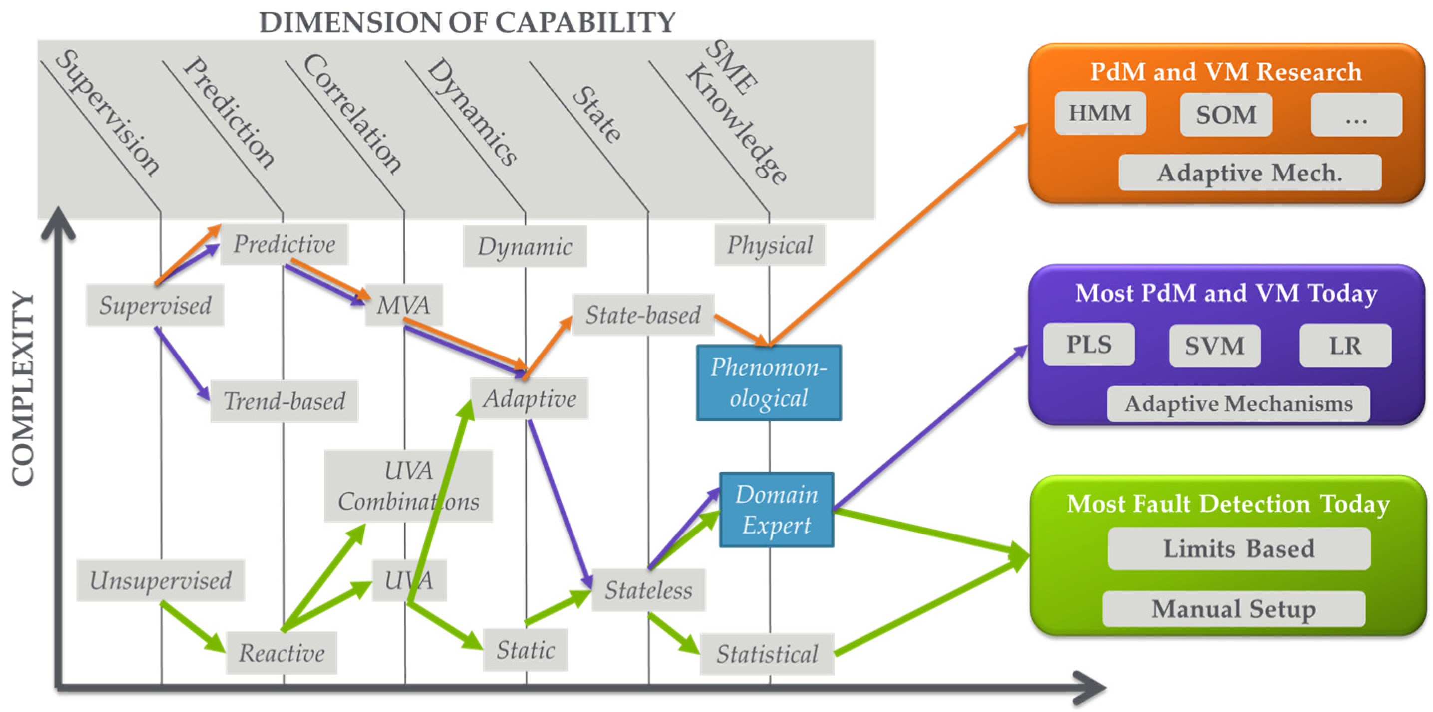
There has been an explosion in analytical approaches over the last decade with many of these analytics developed to take advantage of the big data explosion. One way to identify and categorize these analytics is by defining dimensions of capability in analysis and specifying or plotting analysis capabilities with respect to these dimensions. One perspective of defining a taxonomy for organizing analytics is described in [25]. Figure 3 provides a breakdown of dimensions relevant to analytics in semiconductor manufacturing, with the dimension descriptions as follows [6]:
  • Level of Supervision: This dimension can be thought of as the level of input-output data correlation that the analytic seeks to provide between datasets. In purely unsupervised scenarios, analytics generally operate on a single dataset with no direct objective of correlation to other data sets. A good example is traditional FD, which is actually anomaly detection. Equipment data is analyzed to determine if there is an anomaly in which parameters are anomalous (e.g., out of range). Some EHM applications are also unsupervised. At the other extreme, analytics can focus on determining correlations between “input” and “output” datasets [26,27]. As an example, PdM and VM determine relationships between equipment data (trace or processed, e.g., through FD) and maintenance and metrology measurement data, respectively. Between the two of these are a variety of semi-supervised scenarios in which supervised data may be used strictly for model training, or the input data set is associated with labels such as “good” or “bad” providing a level of supervision.
  • Level of Prediction: This dimension identifies the ability of the analytic to forecast or predict outputs. At one end, analytics can be purely reactive, detecting an event after it has happened. Good examples are traditional fault detection and data mining, in which the analytic provides information based on the understanding that the event has already occurred. At the other end of the spectrum are purely predictive analytics such as PdM where an event is forecasted before it occurs. Note that predictions are usually accompanied by some indication of prediction horizon or time-to-failure and an indication of quality or range of prediction; this is explored further in Section 4.2. Between purely reactive and purely predictive are a number of somewhat predictive capabilities. A good example is trend-based analysis where a generally reactive monitoring capability is analyzed with respect to trends that are extrapolated to anticipate a future event.
  • Level of Correlation Among Parameters Analyzed: This dimension defines how the variables are analyzed with respect to each other in a dataset. At one end we have purely univariate (UVA) analysis in which each parameter is analyzed individually. A large number of FD solutions leverage UVA analysis. Note that this does not mean that parameters are not correlated; it just means that the analysis technique does not explore this correlation. At the other end of the spectrum are multivariate analysis techniques that fully explore parameter correlations. In between are a number of techniques to provide some level of correlation analysis. Good examples are UVA analysis techniques in which variables can be combined in equations or as Boolean variables; these techniques are often available in traditional FD solutions.
  • Level of Incorporation of Dynamics: This dimension characterizes how completely the analytic can track or profile the changes in relationships between parameters over time, e.g., capturing and accommodating drift and shift in a process. At one end are purely static analytics that cannot incorporate dynamics or do not even include a concept of dynamics or time in analysis. At the other end are dynamics that fully address the evolution of relationships over time, e.g., with an evolving model. In between these extremes are a variety of techniques that track or incorporate dynamics to some level. Good examples are adaptive models such as those found in R2R control, in which the model form may not be adjusted over time, but the model (zeroth order term) offset is re-evaluated to track and capture dynamics [13].
  • Level of Incorporation of State: This dimension identifies how well the analytic incorporates the logical progression of system state in the analysis. In other words, it identifies how well the analytic incorporates an understanding of how a system logically operates into the analysis. Note that this is differentiated from the previous dimension where dynamics may be tracked, but logical progression of system state may or may not be understood. At one extreme of this state dimension, the analytic has no concept of state. These analytics are often called “snapshot” because they provide an analysis at an instance of time. At the other end of the spectrum, state-based analytics incorporate state evolution into the analysis.
  • Level of Incorporation of SME: This dimension identifies the level to which SME is incorporated into the analytic. At one end of the spectrum are purely statistical or data-driven analytics where no SME is involved. Some “one-size-fits-all” multivariate (MVA) FD or EHM techniques fall into this category where a dataset is analyzed statistically and an index is reported. At the other end of the spectrum are purely non-statistical physical techniques that rely on complete knowledge of the system with no data-driven component. Between these two extremes are a large number of analytics where SME is incorporated to some extent. The incorporation may be as simple as parameter down selection prior to data-driven analysis, or more complicated as in development of model forms that define the physics of an operation (i.e., phenomenological models) that are tuned using data-driven approaches. Note that, with this dimension, the level, type, method, and formalism by which SME is incorporated can all vary.
Given these dimensions, an analytic or an analysis application can then be defined with respect to the value the capability has in each dimension. As an example of an analytic, principal component analysis (PCA), often used for MVA FD and EHM, is unsupervised, reactive, MVA, generally static, stateless, and does not formally incorporate SME [28]. With respect to analysis applications, FD in semiconductor fabs today (described further below) is largely unsupervised, reactive, UVA, stateless and statistically based with SME incorporated in FD model development [6,10,12,14,29]. Effective PdM solutions today are supervised, predictive, MVA, and stateless with SME incorporated in fault understanding and variable down-selection. In the future as data quality improves, these PdM solutions may become more state-based [6,30].
Defining analytics and analysis applications using these and other dimensions provides a framework for identifying gaps in capability, opportunities for advancement, and, over the longer term, roadmaps for analytics and applications improvement.

3.3. Typical APC Applications and Analytics Approaches in Today’s Semiconductor Manufacturing Facilities

A prerequisite to understanding the roadmap for big data analytics in semiconductor manufacturing is understanding the current state of the art of analytics deployment. The existing analytics base provides a framework for data collection and configuration of big data solutions. Furthermore, it gives insight into the analytics culture in the industry as well as what approaches seem to work given the challenges of data quality, complexity, and dynamics outlined above.
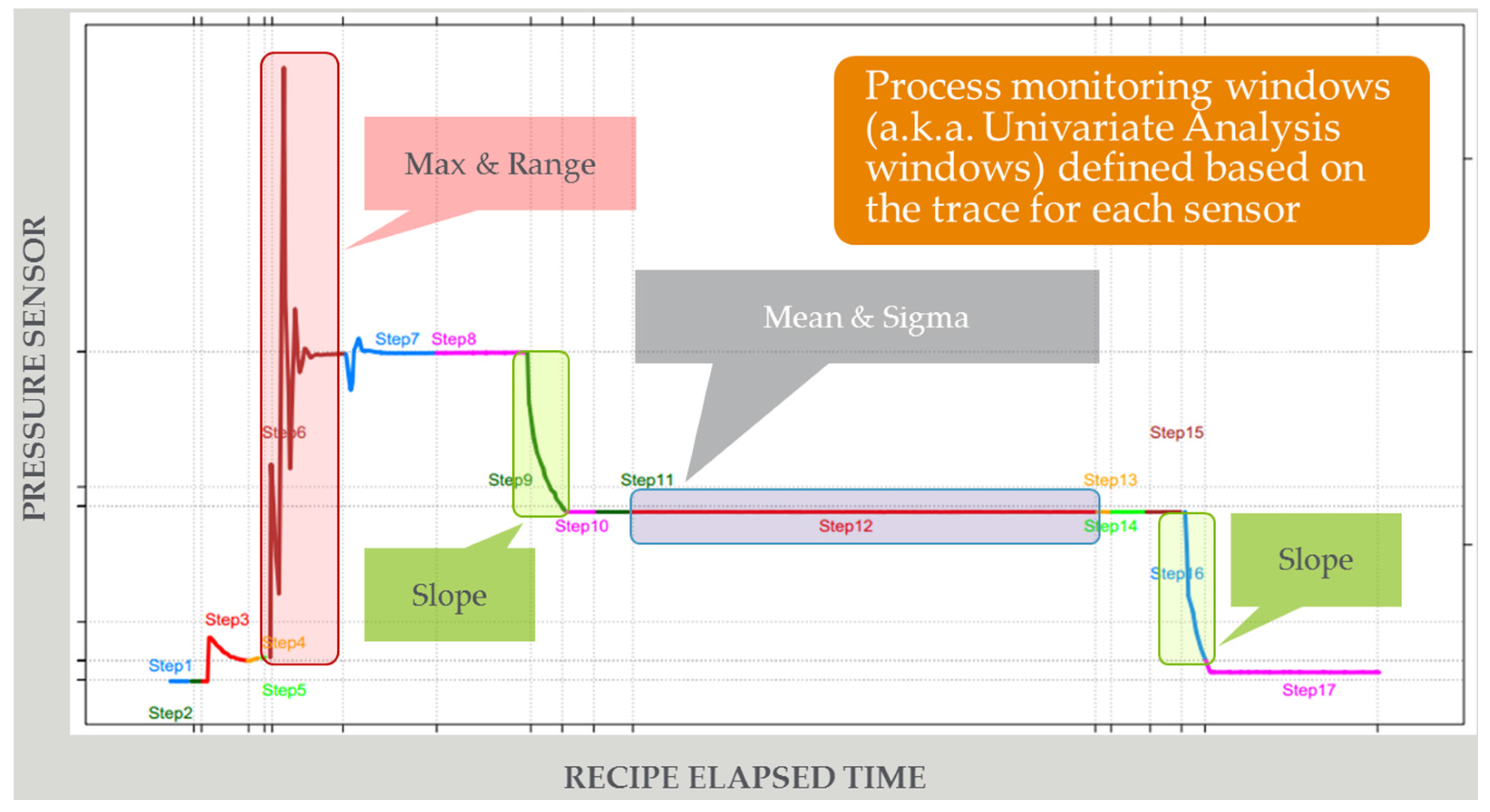
Figure 4 illustrates the approach to FD that is pervasive in the industry today. The vast majority of effective FD solutions are unsupervised and univariate, analyzing process trace data at the end of each run to detect anomalies [29]. There is a focus on identifying features and applying limits tests to determine if there are alarms. SME is used extensively to identify which traces and features to monitor, what limits to set, and how to correlate limits violations to fault classifications. While these methods are generally effective, there are issues of: (1) high numbers of missed and false alarms due largely to the dynamic nature of the processes and lack of correlation to supervised data; (2) process dynamics requiring resetting of models or limits; and (3) significant time required to manually set up and manage models and limits.
Anomaly detection has been extended to unsupervised MVA to support EHM in which single MVA traces are used to indicate the health of the equipment or equipment sub-system. The predominant method used here is PCA, with other methods employed including one-class support vector machine (SVM), k-nearest neighbors (k-NN), auto-associative neural network, and hidden Markov models (HMMs) [26,31,32,33,34]. When an alarm occurs, a decomposition of the MVA model can provide a Pareto of contributors to a fault, aiding in classification. EHM systems are easier to configure and manage from a user interface perspective than traditional univariate FD systems, however, they generally are highly susceptible to noise and other data quality issues, are difficult to maintain in the face of system dynamics, and, like FD, are unsupervised, so there is no guarantee that an anomaly is actually a fault.
Model-based process control (MBPC) or R2R control is also employed extensively in semiconductor manufacturing [12]. There is a large literature base devoted to the evolution of this capability over the past two decades. The challenge for MBPC is that processes in semiconductor manufacturing are poorly observable, highly dynamic and subject to a large number of disturbances. It was determined early on that simple linear solutions that use exponentially weighted moving average (EWMA) filtering were effective [13]. Over the years, there has been a migration to more state-based solutions and single threaded solutions, in which a single model can be applied to control the production of multiple products in multiple context environments [13,15,35].

3.4. Emerging APC Analytics Applications and Analytics Trends in Semiconductor Manufacturing Facilities

The recent evolution in semiconductor manufacturing APC applications reflects a movement from a more reactive to predictive and even proactive approach to factory control [6,17,20]. Failure detection is being augmented with failure prediction to support capabilities such as PdM. Metrology measurement prediction using VM is being leveraged to reduce cycle times due to metrology delay and improve process capability [36,37]. Predictive scheduling, first at the process level and eventually at the across-fab level is beginning to be leveraged to lessen some capacity constraints [38]. Yield prediction with feedback into process control, production scheduling, and maintenance scheduling is being investigated so that fab-wide control can be optimized to yield-throughput objectives [39]. Eventually, these predictive solutions will extend more horizontally, incorporating upstream and downstream supply chain [1,2,3,17,20].
This evolution is relying heavily on the big data explosion in the face of the aforementioned industry data challenges. Specifically, support for larger volumes and longer archives of data has (to some extent) enabled predictive solutions to decipher complexities of multivariate interactions of parameters, characterize system dynamics, reject disturbances, and filter out data quality issues. In many cases, the algorithms in these solutions have to be rewritten to take advantage of the parallel computation afforded by big data solutions in order to process the data in a timely manner, or (as will be discussed later) new algorithms are leveraged that are more big data environment friendly. As an example, earlier predictive solutions relied on single core CPU and serial processing. With big data, popular techniques such as partial least squares (PLS) and support vector machines (SVM) are rewritten to allow parallel computation on a server farm [40,41]. Likewise, unsupervised data exploration techniques such as self-organizing map (SOM) and generative topographic mapping (GTM) are rewritten to consume large amount of data enabling people to quickly gain insights from the data [42,43]. Similarly, time-consuming techniques such as HMM and particle swarm optimization can be rewritten to become computationally far more efficient [44,45].
However, a plethora of techniques and a massive amount of data do not necessarily lead to more insights and predictive capability. It is the author’s belief that no one approach or combination of approaches will be a panacea, but rather approaches will be customized to application spaces in terms of objective, available data, data quality, etc. Regardless of the approach, it is believed that SME will continue to guide solution development and maintenance.

4. Case Studies of Big Data Analytics Approaches in Semiconductor Manufacturing

4.1. Next Generation Fault Detection and Classification (NG-FDC)

While fault detection has been an integral component of semiconductor manufacturing for at least a decade and provides significant required benefits (such as scrap reduction, quality improvement, and equipment maintenance indications), it continues to be plagued by high setup costs and high rates of false and missed alarms. This fact was underscored at the 2015 Integrated Measurement Association APC Council meeting, held in conjunction with the 2015 APC Conference ([46] and [6]). Here, top APC specialists from the microelectronics manufacturing user and supplier communities reached consensus on the following points: (1) “[There is a] need for automation of front-end of FD from model building to limits management, but keep in process and equipment expertise”; and (2) a major pain point in today’s FDC systems is false and/or missed alarms. This fact was verified in the field; for example, a deployment expert indicated that it often takes up to two weeks to correctly configure univariate FD for a process tool, including collecting data, refining limits, and correlating limits violations to actual events of importance, and even after this process is completed there are often too many false alarms or missed alarms associated with a particular FD model [29].
The big data evolution afforded an opportunity in semiconductor manufacturing to provide an improved FDC capability that addresses these key pain points [6,29,47]. The FD portion of this NG-FDC technology contains two key components. The first component is trace level automated analysis: This component uses multivariate analysis techniques that are data-driven to detect and characterize anomalies [48]. It has the advantage of a one-size-fits-all approach to analysis that is easy to manage. It also can detect patterns in data that are not readily apparent or not suggested by an SME. However, because it does not incorporate SME very well, it can result in high numbers of false and missed alarms, lack appropriate prioritization of alarms, etc. [6,29].
The second component, semi-automated trace partitioning, feature extraction, and limits monitoring, directly addresses the pain points identified in the aforementioned APC Council industry meeting. The approach uses trace partitioning, feature extraction, and limits setting techniques that are semi-automated, allowing the incorporation of SME. With this approach, model building times can be drastically reduced by orders of magnitude depending on the level of SME incorporation, and results indicate that false and missed alarm rates are improved ([47] and [29] and [6]).
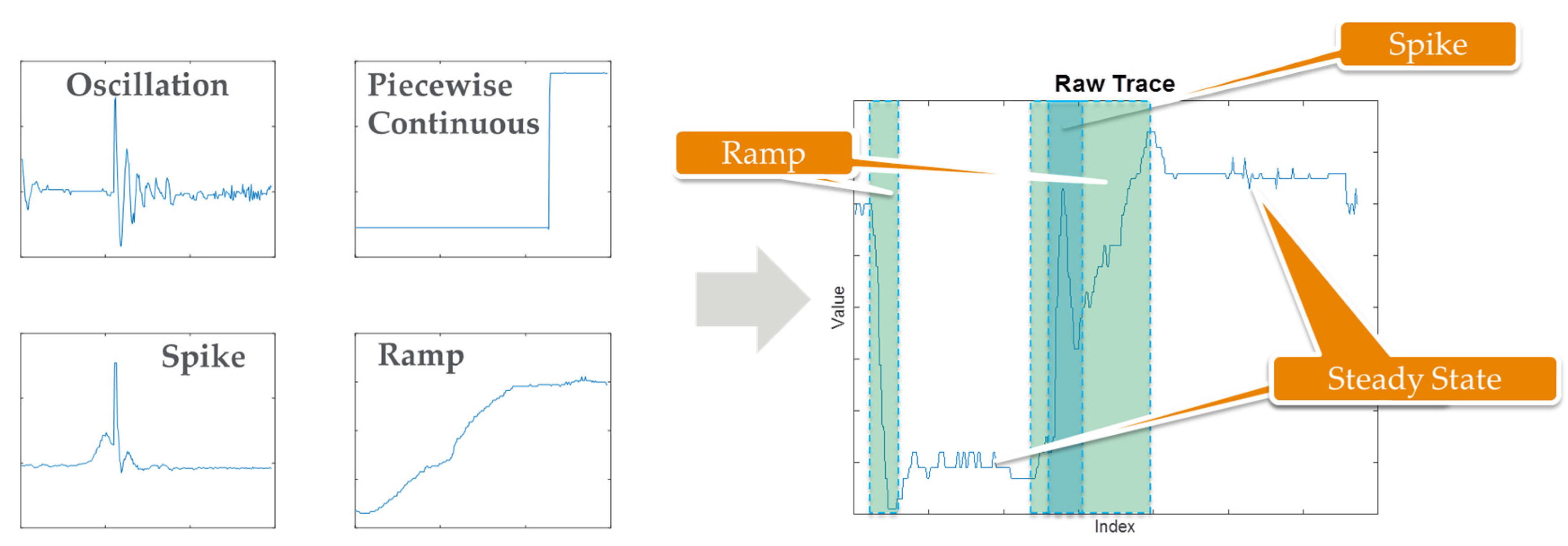
The trace partitioning component is illustrated in Figure 5. Common patterns of interest are determined by analyzing historical data and consulting with SMEs. Indeed, many of these patterns are signals that would typically result from a physical process such as turning on a switch (piecewise continuous step function), vibration or underdamped actuation (oscillation), momentary disturbance (spike), or drift (ramp). Using a myriad of search techniques organized in a hierarchical fashion, the boundaries of these features are determined and the sensor trace is partitioned; these techniques are described in more detail in [47]. Then techniques specific to each feature type are used to extract each feature model. Note that the solution is configurable in that there are settable parameters for each feature type used to: (1) distinguish a feature (sensitivity); and (2) distinguish between features (selectivity). In addition, the method is extensible in that additional feature types can be added to the detection hierarchy. SME is used to: (1) select the sensitivity and selectivity parameters; (2) choose, among the candidate features, which to extract and monitor for FD; and (3) fine tune partitions and model parameters as necessary.
Figure 6 summarizes the results of applying this NG-FDC capability to a public etch data set ([47] and [6]). Three approaches to analysis were compared: (1) whole trace statistics in which whole trace mean and variance were used to determine faults; (2) manual windowing in which best guess manual techniques were used for partitioning and feature extraction; and (3) semi-automated feature extraction as defined above was employed for FD. A SOM clustering approach was used to optimize the alarm limits setting for each approach [42]. The results indicate the semi-automated trace partitioning and feature extraction outperforms the other approaches in terms of reduced false alarms (false positive rate) and missed alarms (1minus true positive rate).
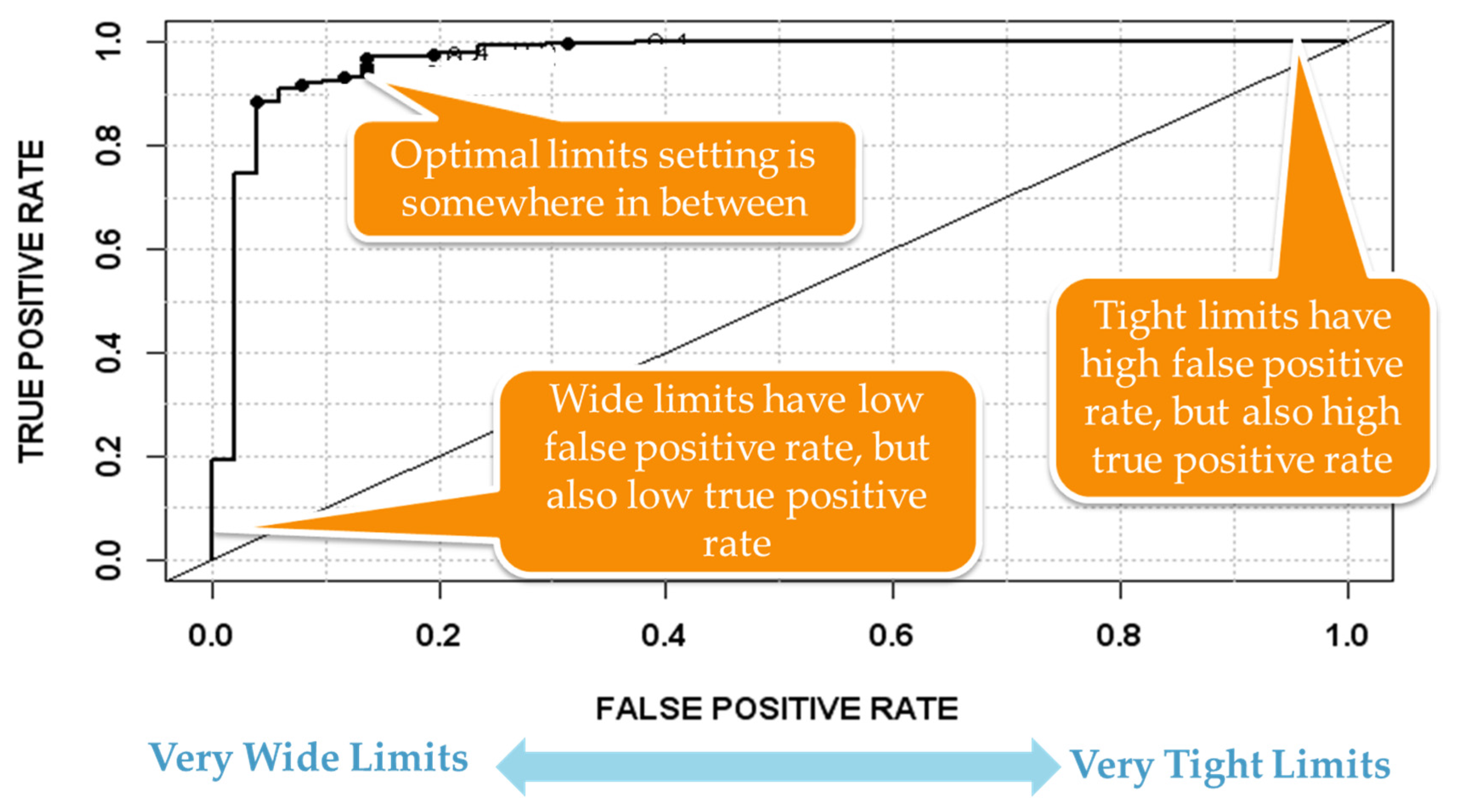
With semi-automated trace partitioning and feature extraction in place, a candidate set of FD models can automatically be presented to the SME for down selection. The down selection process can be aided if supervised data is available as the relationship between features and process or equipment faults can be determined. After the appropriate final list of FD models has been determined, monitoring limits must be set to provide a balance between false and missed alarms. As shown in Figure 7, a receiver operating characteristic (ROC) can be plotted for each FD model in which the limits are adjusted [49]. If the limits are very wide, the model is insensitive so there are few false alarms, but high levels of missed alarms. If the limits are very tight, the reverse is true. The challenge is to determine an optimal limit setting that balances the occurrences of true and false positives to the cost of these events in the particular application. A solution to this problem involves plotting a cost function on top of the ROC and is detailed in [50].
After models and limits have been set up for a system, they must be managed in an environment that is oftentimes very dynamic, with numerous process and product disturbances and context changes (e.g., product changes). Model and limits management remains a challenge, but is often accomplished with a variety of tools for model pre-treatment to address context, model continuous update to support process dynamics, and model and limits update triggering and rebuilding or retargeting [51].

4.2. Predictive Maintenance (PdM)

The concept of PdM in semiconductor industries grew out of the high cost of unscheduled downtime that includes cost of yield loss and maintenance in addition to lost production time. Practitioners realized that univariate FD systems could sometimes be leveraged to detect trends in a particular variable; these trends could then be extrapolated to determine approximate remaining useful life (RUL) of a particular component. Scheduled maintenance could then be adjusted to reduce the occurrence of unscheduled downtime or extend uptime (if scheduled maintenance is overly conservative). However, as noted earlier, semiconductor manufacturing processes are characterized by complexity and variability, and are subject to frequent disturbances. As a result, the univariate FD extrapolation mechanisms for predicting maintenance as mentioned above are generally not optimal, robust or even maintainable.
The approach to PdM that seems to be most effective in semiconductor manufacturing uses FD or NG-FDC output data along with maintenance data, context data, process data, and potentially process metrology data to develop predictive models using off-line using MVA techniques [6,30]. The goal, as shown in Figure 8a, is to develop a predictor that allows the user to predict a future failure along with obtaining an estimated time to failure (TTF) horizon and some indication of confidence in or range of the prediction. The failure indication trigger can be as simple as a threshold (as shown) or a more complex analysis of a degradation profile. The trigger is set based on the confidence of the prediction, but also to provide a TTF that useful to the user (e.g., the approximate time necessary to align maintenance resources).
The off-line modeling process used to achieve this goal is illustrated in Figure 8b. Note that techniques for data aggregation, treatment, feature selection, model building and analysis, and model optimization through cost-benefit analysis are largely the same as the techniques used in NG-FDC. Indeed, these same techniques can be leveraged for other predictive capabilities such as VM and yield prediction. In the case of PdM, large amounts of data are needed so that failure prediction models accommodate factors such as the potentially long degradation profile of some failure types (which could be months or years), large number of failures types and failure modes within each failure type, and the impact to process variability and context (e.g., product changes). There often is not sufficient data to fully characterize a particular piece of equipment using purely data-driven methods, and this problem is often not solvable with improved big data practices because the process or equipment changes enough over time to make longer term data histories somewhat irrelevant. Thus, SME of equipment, equipment components, and processes is usually leveraged heavily in PdM model building and maintenance.
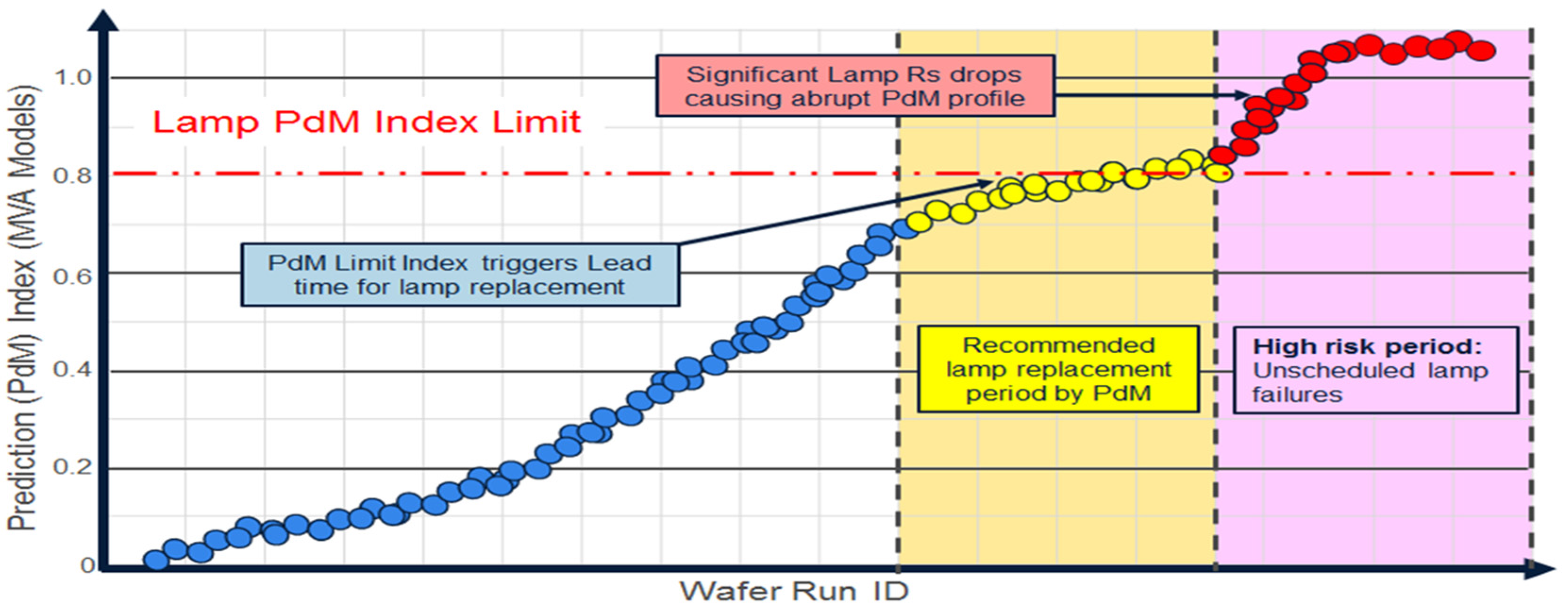
An example of application of PdM for an epitaxial process is shown in Figure 9. Epitaxial equipment is used to grow films such as oxidation on semiconductor surfaces. Banks of lamps are used to create heat so that a film is deposited or grown to a precise thickness evenly. Utilizing straight-forward UVA FD, lamp replacement can be predicted only 4–5 h in advance, which leads to a high risk of unexpected lamp failures and unexpected downtime. Utilizing MVA PdM, lamp failure can be predicted five days in advance with about 85% accuracy, reducing unscheduled downtime and increasing throughput. Potential for impact is estimated at $108K (USD) per process chamber per year. The solution is robust to process disturbances including R2R control process tuning; virtual sensor models were developed to decouple disturbances from the prediction signal [6].

5. Discussion: The Evolving Big Data Landscape and Analytics

The analytics landscape in semiconductor manufacturing continues to evolve in part due to SM directives and innovation, but also due to the evolution of big data in an analytics landscape in and outside of manufacturing. In this section, a few of the factors impacting the evolution of SM analytics are explored.

5.1. Big Data Architectures

The move to big data analytics to support SM concepts in semiconductor manufacturing includes the move to more big data friendly platforms. As an example, Apache Hadoop is an open-source software framework for storage and large-scale processing of datasets on clusters of commodity hardware [52]. Hadoop leverages parallel processing and scalability capabilities to provide solutions tailored to large time-series datasets such as trace data. Most large semiconductor manufacturers are incorporating or at least evaluating big data platforms with the predominant choice being Hadoop [46]. In general, conversion to a Hadoop infrastructure will provide a number of benefits, including: (1) lower cost of ownership (COO) of data solutions; (2) more efficient data storage; (3) improved query processing speeds; (4) improved analytics performance; and (5) better enabling of predictive analytics, with analysis quantifying these advantages [53]. However, these platforms are generally not suited to real-time or time critical on-line analytical operations on the factory floor. Thus, near-future factory floor data management solutions will likely be a Hadoop or other big data-friendly ecosystem combined with a small transactional component probably best suited to a relational database, the latter being used to support time critical (i.e., “real-time”) analysis and associated execution. A migration path from traditional relational to more big data-friendly architectures must be supported so that the advantages of both database structures can be leveraged, and the share of tasks assigned to the big data-friendly portion can be adjusted as innovation allows these architectures to support more and more time critical on-line tasks [21,29,53].

5.2. Emergence of Artificial Intelligence and Other Big Data-Friendly Analytics

The term “AI” can be used to describe any device or analytic that perceives its environment and takes action to achieve a goal. Today, the term is often used to refer to the concept of these devices or analytics mimicking the function of the human brain, such as in self-driving automobile applications [54]. Artificial neural networks (ANN), which is an example of this type of analytic, has been around for decades. These types of AI analytics have seen resurgence as part of the big data evolution. For example, Deep Learning is a technique that is very similar to structured ANN and leverages hierarchical abstraction for improved quality and speed of high-volume data analysis. As noted in [55], “Deep Learning can be utilized for addressing some important problems in Big Data Analytics, including extracting complex patterns from massive volumes of data, semantic indexing, data tagging, fast information retrieval, and simplifying discriminative tasks.” Deep Learning techniques benefit from increased data volumes in big data environments and uses data-driven supervised techniques to find relationships in data. The main drawback in on-line manufacturing analytics applications is its inability to incorporate SME in model development and maintenance [56]. In addition, developed models are generally not explicitly available so it is often difficult to assess the future robustness of these models. Recently, there have been research efforts focused on combining SME with AI techniques; these techniques hold promise for future application on the manufacturing floor [57].
Another analytical capability that is receiving significant attention in industrial big data applications is background analysis by solutions often termed as “crawlers” [53]. These application mine data in the background looking for particular patterns or analytical results of interest, such as a part nearing fault, and then asynchronously inform a consuming application such as a factory control system so that appropriate action can be taken. This approach allows analytics to be performed in the background so that they can be better managed with higher priority tasks such as factory control. It also allows the development and management of these diagnostics and prognostics to be more re-configurable.

5.3. Realizing the Complete Smart Manufacturing Vision

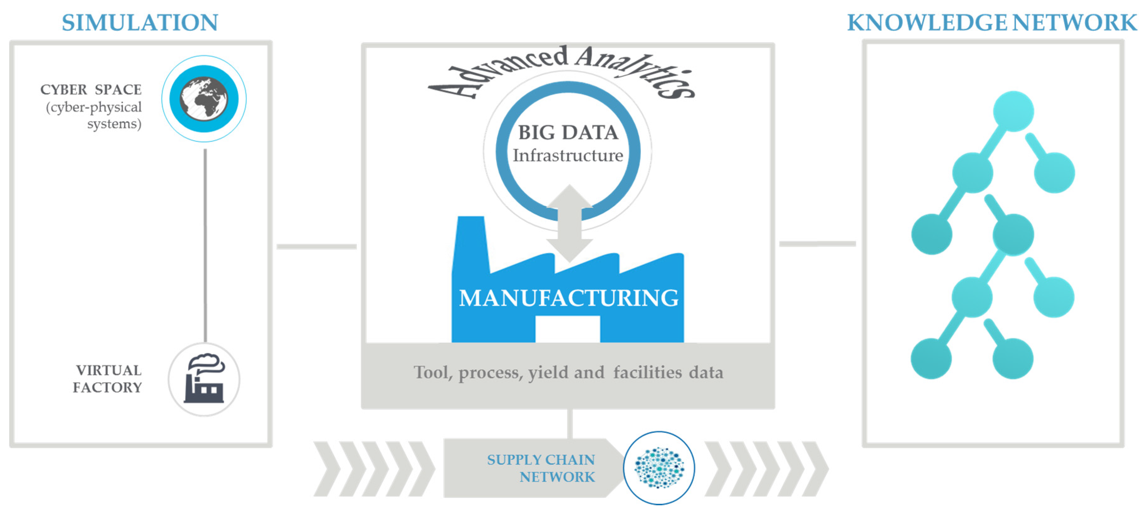
A cursory review of literature reveals that there are many depictions of the SM vision. Figure 10 shows a vision that has been proposed for the semiconductor manufacturing industry ([17] and [6]), which illustrates some common SM themes in the industry such as:
  • Integration with the supply chain network: The smart factory will become an integral part of the supply chain with factory optimization part of overall supply chain optimization. The tighter connectivity will allow for leaner operation, higher flexibility of operation, improved response to demand, and better traceability for analytics such as warranty recall investigation. It will also represent an integration of the SM vision up and down the supply chain.
  • Improved use of cyber-physical systems (CPS): CPS refers to the “tight conjoining of and coordination between computational and physical resources” [58]. While systems that generally integrate computational and physical resources have been in existence for some time, future systems will continue to improve in terms of “adaptability, autonomy, efficiency, functionality, reliability, safety, and usability.” Big data analytics will play an important role in the advancement of these CPSs.
  • Incorporating the simulation space and the concepts of virtual factory and digital twin: the prediction vision for semiconductor manufacturing is identified as “a state of fab operations where (1) yield and throughput prediction is an integral part of factory operation optimization, and (2) real-time simulation of all fab operations occurs as an extension of existing system with dynamic updating of simulation models.” [19,20]. The latter concept, which is a component of the CPS vision, is often referred to as “digital twin.” Many of the predictive applications being developed in the industry today will likely continue to evolve to more directly support this vision.
  • Leveraging big data architectures infrastructures: These infrastructures include the data management, but also the analytics and applications that leverage the infrastructure to improve SM operation.
  • Leveraging advanced analytics: As noted throughput this paper, the benefits of the big data evolution will be provided primarily by applying analytics that take advantage of big data to improve existing capabilities such as FDC or realize new capabilities such as prediction.
  • Reliance on a knowledge network: The overall consensus of the SM vision in semiconductor manufacturing is that SME knowledge will continue to be leveraged as an integral part of analytical solutions, with cooperation required between users, solution suppliers, and equipment and components manufacturers to support a service-based approach for delivering and maintain solutions [19,20]. Issues such as data sharing and partitioning, intellectual property security, and managing solutions in the cloud have all come to the forefront as part of the move to enhance support for the cooperative knowledge network [19,20,25,46].

6. Conclusions

Smart manufacturing is an evolution in manufacturing capabilities that is focused on improving operations through tighter integration, linking of physical and cyber capabilities, leveraging the big data evolution, and taking advantage of information and analytics. This evolution has been occurring unevenly across industries, thus an opportunity exists to look at other industries to help determine solution and roadmap paths for a particular industry such as biochemistry or biology. Profiling and comparing these analytics using a dimension approach allows for identifying capabilities as well as gaps and roadmaps for future improvement.
The semiconductor manufacturing industry is characterized by precise processing requirements, highly complex and dynamic equipment and processes, and issues in manufacturing data quality. In light of these issues, experience in analytical solution deployment reveals that incorporating SME is usually required to realize robust and maintainable solutions. This fact is highlighted in case studies for next generation fault detection and classification, and predictive maintenance. Analytics will continue to be leveraged at higher rates in SM corresponding in large part with the big data evolution. While methods for data quality improvement and SME incorporation will evolve as problems are solved, these factors will likely remain as key components of the analytics roadmap for SM.
Longer term the vision of SM will continue to leverage analytics to promote improvements in cyber-physical linkages, including the use of the concepts of virtual factory and digital twin. Improved integration up and down the supply chain will serve to advanced factory capabilities such as throughput, quality, and efficiency, but also will tend to bring a level of commonality to SM concepts and implementation roadmaps that should help facilitate a consistent SM vision across the enterprise.

Acknowledgments

The authors would like to acknowledge technical and editing contributions from Brad Schulze, Michael Armacost, Heng Hao and Todd Snarr at Applied materials; Chao Jin, Yuan Di and Xiaodong Jia at the University of Cincinnati; and Felipe Lopez at the University of Michigan. The authors would also like to acknowledge the following organizations for their support of the development of semiconductor manufacturing analytics: The Integrated Measurement Association and the Advanced Process Control Conference, The International Roadmap for Devices and Systems, and The Center for Intelligent Maintenance. A portion of the background research for this work was supported in part by the National Science Foundation (NSF) under award number CSR 1544678.

Author Contributions

J.M. conceived of, conducted the background research for, and wrote the manuscript. J.I. contributed to the discussion in Section 3.4 and provided some of the algorithm references. A large portion of this article is a literature survey with contribution indicated through reference.

Conflicts of Interest

The authors declare no conflict of interest.

Abbreviations

The following abbreviations are used in this manuscript:
AAKRAuto-Associative Kernel Regression
AIArtificial Intelligence
ANNArtificial Neural Network
APCAdvanced Process Control
BDBig Data
CPSCyber-Physical System
EHMEquipment Health Monitoring
ERPEnterprise Resource Planning
EWMAExponentially Weighted Moving Average
FCFault Classification
FDFault Detection
FDCFault Detection and Classification
GTMGenerative Topographic Mapping
HMMHidden Markov Model
IoTInternet of Things
k-NNk-Nearest Neighbors
LRLinear Regression
MESManufacturing Execution System
MVAMultivariate Analysis
NG-FDCNext Generation Fault Detection and Classification
PCAPrincipal Component Analysis
PdMPredictive Maintenance
PLSPartial Least Squares or Project on Latent Structures
R2RRun-to-Run (control)
ROCReceiver Operating Characteristic
RULRemaining Useful Life
SMSmart Manufacturing
SMESubject Matter Expertise
SOMSelf-Organizing Map
SPCStatistical Process Control
SVMSupport Vector Machines
TTFTime To Failure
UVAUnivariate Analysis
VMVirtual Metrology

References

  1. Wikipedia: Smart Manufacturing. Available online: https://en.wikipedia.org/wiki/Smart_manufacturing (accessed on 1 June 2017).
  2. Davis, J.; Edgar, T.; Porter, J.; Bernaden, J.; Sarli, M. Smart manufacturing, manufacturing intelligence and demand-dynamic performance. Comput. Chem. Eng. 2012, 47, 145–156. [Google Scholar] [CrossRef]
  3. Lee, J.; Kao, H.A.; Yang, S. Service Innovation and smart analytics for industry 4.0 and big data environment. Proced. Cirp 2014, 16, 3–8. [Google Scholar] [CrossRef]
  4. Thoben, K.-D.; Wiesner, S.; Wuest, T. “Industrie 4.0” and smart manufacturing—A review of research issues and application examples. Int. J. Autom. Technol. 2017, 11, 4–16. [Google Scholar] [CrossRef]
  5. Kagermann, H.; Wahlster, W. Industrie 4.0: Smart Manufacturing for the Future; Germany Trade and Invest: Berlin, Germany, 2016. [Google Scholar]
  6. Moyne, J.; Iskandar, J.; Armacost, M. Big Data Analytics Applied to Semiconductor Manufacturing. In Proceedings of the AIChE 3rd Annual Big Data Analytics Conference, San Antonio, TX, USA, 28 March 2017. [Google Scholar]
  7. Romero-Torres, S.; Moyne, J.; Kidambi, M. Towards Pharma 4.0; Leveraging Lessons and Innovation from Silicon Valley. American Pharmaceutical Review. 5 February 2017. Available online: http://www.americanpharmaceuticalreview.com/Featured-Articles/333897-Towards-Pharma-4-0-Leveraging-Lessons-and-Innovation-from-Silicon-Valley/ (accessed on 1 June 2017).
  8. Evans, P. Initiatives for Applying Smart Manufacturing to the Continuous Processing Industries. Available online: https://www.aiche.org/sites/default/files/community/291721/aiche-community-site-page/315581/initiativesforapplyingsmartmanufacturingtothecontinuous-rev1.pdf (accessed on 1 June 2017).
  9. Handy, J. What’s It Like in a Semiconductor Fab. Forbes 2011. Available online: https://www.forbes.com/sites/jimhandy/2011/12/19/whats-it-like-in-a-semiconductor-fab/#2ecf8c9745ef (accessed on 1 June 2017).
  10. May, G.S.; Spanos, C.J. Fundamentals of Semiconductor Manufacturing and Process Control; IEEE, Wiley-Interscience: Hoboken, NJ, USA, 2006. [Google Scholar]
  11. Sarfaty, M.; Shanmugasundram, A.; Schwarm, A. Advance Process Control solutions for Semiconductor Manufacturing. In Proceedings of the IEEE Advanced Semiconductor Manufacturing Conference, Boston, MA, USA, 30 April 2002. [Google Scholar]
  12. Moyne, J. Introduction to and Practical Application of APC: A Tutorial. In Proceedings of the Advanced Process Control Conference XXVII, Phoenix, AZ, USA, 17–20 October 2016. [Google Scholar]
  13. Moyne, J.; Del Castillo, E.; Hurwitz, A. Run-to-Run Control in Semiconductor Manufacturing; CRC Press: Boca Raton, FL, USA, 2000. [Google Scholar]
  14. Dimond, K.; Nowalk, T.; Yelverton, M. Implementing and Assessing the Value of Factory-Wide Fault Detection Deployment at a High Volume Foundry. In Proceedings of the Advanced Process Control Symposium XV, XXX, Colorado Springs, CO, USA, 9–12 September 2003. [Google Scholar]
  15. Moyne, J. A Blueprint for Enterprise-Wide Deployment of APC. In Proceedings of the Advanced Process Control Symposium XXI, XXX, Ann Arbor, MI, USA, 27–30 September 2009. [Google Scholar]
  16. Hu, C. 3D FinFET and other sub-22nm transistors. In Proceedings of the 19th IEEE International Symposium on the Physical and Failure Analysis of Integrated Circuits (IPFA), Marina Bay Sands, Singapore, 2–6 July 2012. [Google Scholar]
  17. Hasserjian, K. Emerging Trends in IC Manufacturing Analytics and Decision Making. Keynote. In Proceedings of the Advanced Process Control Conference XXVII, Phoenix, AZ, USA, 17–20 October 2016. [Google Scholar]
  18. International Roadmap for Devices and Systems (IRDS): Beyond CMOS (Emerging Research Device) White Paper, 2016 Edition. Available online: http://irds.ieee.org/images/files/pdf/2016_BC.pdf (accessed on 1 June 2017).
  19. International Technology Roadmap for Semiconductors (ITRS): Factory Integration Chapter, 2016 Edition. Available online: www.itrs2.net (accessed on 1 June 2017).
  20. International Roadmap for Devices and Systems (IRDS): Factory Integration White Paper, 2016 Edition. Available online: http://irds.ieee.org/images/files/pdf/2016_FI.pdf (accessed on 1 June 2017).
  21. Moyne, J. International Technology Roadmap for Semiconductors (ITRS) Factory Integration, 2015: Summary of Updates and Deep Dive Into Big Data Enhancements. In Proceedings of the APC Conference XXVII, Austin, TX, USA, 12–14 October 2015. [Google Scholar]
  22. Rebooting the IT Revolution: A Call to Action; Semiconductor Industry Association and Semiconductor Research Corporation: Washington, DC, USA, 4 January 2016. Available online: https://www.src.org/newsroom/press-release/2016/758/ (accessed on 1 June 2017).
  23. Big Data Standards. Available online: http://bigdata.ieee.org/standards (accessed on 1 June 2017).
  24. SEMI E133-1014: Specification for Automated Process Control Systems Interface. Semiconductor Equipment and Materials International, 2014. Available online: http://www.semi.org/en/Standards/StandardsPublications (accessed on 1 June 2017).
  25. Lopez, F.; Saez, M.; Shao, Y.; Balta, E.C.; Moyne, J.; Mao, Z.M.; Barton, K.; Tilbury, D. Categorization of anomalies in smart manufacturing systems to support the selection of detection mechanisms. IEEE Robot. Autom. Lett. 2017, 2, 1885–1892. [Google Scholar] [CrossRef]
  26. Wuest, T. Identifying Product and Process state Drivers in Manufacturing Systems Using Supervised Machine Learning; Springer: New York, NY, USA, 2015. [Google Scholar]
  27. Wuest, T.; Irgens, C.; Thoben, K.-D. An approach to quality monitoring in manufacturing using supervised machine learning on product state data. J. Intell. Manuf. 2014, 25, 1167–1180. [Google Scholar] [CrossRef]
  28. Johnson, R.A.; Wichern, D.W. Applied Multivariate Statistical Analysis; Pearson Education International: London, UK, 2002. [Google Scholar]
  29. Moyne, J.; Schulze, B.; Iskandar, J.; Armacost, M. Next Generation Advanced Process Control: Leveraging Big Data and Prediction. In Proceedings of the 27th Annual Advanced Semiconductor Manufacturing Conference (ASMC 2016), Saratoga Springs, NY, USA, 16–19 May 2016. [Google Scholar]
  30. Iskandar, J.; Moyne, J.; Subrahmanyam, K.; Hawkins, P.; Armacost, M. Predictive Maintenance in Semiconductor Manufacturing: Moving to Fab-Wide Solutions. In Proceedings of the 26th Annual Advanced Semiconductor Manufacturing Conference (ASMC 2015), Saratoga Springs, NY, USA, 3–6 May 2015. [Google Scholar]
  31. Ma, J.; Perkins, S. Time-Series Novelty Detection Using One-Class Support Vector Machines. In Proceedings of the International Joint Conference on Neural Networks, Portland, OR, USA, 20–24 July 2003. [Google Scholar]
  32. Hautamaki, V.; Karkkainen, I.; Franti, P. Outlier Detection Using k-Nearest Neighbour Graph. In Proceedings of the 17th International Conference on Pattern Recognition, Cambridge, UK, 23–26 August 2004; pp. 430–433. [Google Scholar]
  33. Markou, M.; Singh, S. Novelty detection: A review—Part 2: Neural network based approaches. Signal Process. 2003, 83, 2499–2521. [Google Scholar] [CrossRef]
  34. Markou, M.; Singh, S. Novelty detection: A review—Part 1: Statistical approaches. Signal Process. 2003, 83, 2481–2497. [Google Scholar] [CrossRef]
  35. Wang, J.; He, Q.P.; Edgar, T.F. State estimation in high-mix semiconductor manufacturing. J. Process Control 2009, 19, 443–456. [Google Scholar] [CrossRef]
  36. Khan, A.; Moyne, J.; Tilbury, D. Fab-wide control utilizing virtual metrology. IEEE Trans. Semicond. Manuf. Spec. Issue Adv. Process Control 2007, 20, 364–375. [Google Scholar] [CrossRef]
  37. Cheng, F.-T.; Kao, C.-A.; Chen, C.-F.; Tsai, W.-H. Tutorial on applying the VM technology for TFT-LCD manufacturing. IEEE Trans. Semicond. Manuf. 2015, 28, 55–69. [Google Scholar]
  38. Kidambi, M.; Krishnaswamy, S.; Marteney, S.; Moyne, J.; Norman, D.; Webb, J. Improving Lithography Throughput and Minimizing Waste Using Predictive Multi-area Scheduling. In Proceedings of the SPIE Metrology Inspection, and Process Control for Microlithography XXV Conference, San Jose, CA, USA, 29 March 2012. [Google Scholar]
  39. Moyne, J.; Schulze, B. Yield management enhanced advanced process control system (YMeAPC): Part I, description and case study of feedback for optimized multi-process control. IEEE Trans. Semicond. Manuf. Spec. Issue Adv. Process Control 2010, 23, 221–235. [Google Scholar] [CrossRef]
  40. Geladi, P.; Kowalski, B.R. Partial least-squares regression: A tutorial. Anal. Chim. Acta 1986, 185, 1–17. [Google Scholar] [CrossRef]
  41. Drucker, H.; Burges, C.J.C.; Kaufman, L.; Smola, A.; Vapnik, V. Support vector regression machines, advances in neural information processing systems 9. 1997, 9, 155–161. [Google Scholar]
  42. Kohonen, T. The self-organizing map. Neurocomputing 1998, 21, 1–6. [Google Scholar] [CrossRef]
  43. Bishop, C.; Svensén, M.; Williams, C.K.I. GTM: The generative topographic mapping. Neural Comput. 1998, 10, 215–234. [Google Scholar] [CrossRef]
  44. Rabiner, L.; Juang, B. An Introduction to hidden markov models. IEEE ASSP Mag. 1986, 3, 4–16. [Google Scholar] [CrossRef]
  45. Kennedy, J.; Eberhart, R. Particle Swarm Optimization. In Proceedings of the IEEE International Conference on Neural Networks, Perth, WA, Australia, 27 November–1 December 1995. [Google Scholar]
  46. Integrated Measurement Association (IMA) APC Council Meeting Minutes: October 2015 Meeting. Available online: http://info.cimetrix.com/blog/default-blog/blog/2015_advanced_process_control_conference (accessed on 1 June 2017).
  47. Chao, J.; Di, Y.; Moyne, J.; Iskandar, J.; Hao, H.; Schulze, B.; Armacost, M.; Lee, J. Extensible framework for pattern recognition-augmented feature extraction (PRAFE) in robust prognostics and health monitoring. In Preparation for Submission to IEEE Trans. Semicond. Manuf.
  48. Ho, T.; Wang, W.; Villareal, G.; Hall, C.; McCormick, E. Dynamic Full Trace FDC. In Proceedings of the Advanced Process Control Conference XXVII, Phoenix, AZ, USA, 17–20 October 2016. [Google Scholar]
  49. Hanley, J.A.; McNeil, B.J. The meaning and use of the area under a receiver operating characteristic (roc) curve. Radiology 1982, 143, 29–36. [Google Scholar] [CrossRef] [PubMed]
  50. Moyne, J. Method and Apparatus for Optimizing Profit in Predictive Systems. U.S. Patent 20,150,105,895, 5 February 2015. [Google Scholar]
  51. Iskandar, J.; Moyne, J. Maintenance of Virtual Metrology Models. In Proceedings of the 27th Annual Advanced Semiconductor Manufacturing Conference (ASMC 2016), Saratoga Springs, NY, USA, 16–19 May 2016. [Google Scholar]
  52. Wikipedia: Apache_Hadoop. Available online: http://en.wikipedia.org/wiki/Apache_Hadoop (accessed on 1 June 2017).
  53. Moyne, J.; Samantaray, J.; Armacost, M. Big data capabilities applied to semiconductor manufacturing advanced process control. IEEE Trans. Semicond. Manuf. 2016, 29, 283–291. [Google Scholar] [CrossRef]
  54. Wikipedia: Artificial Intelligence. Available online: https://en.wikipedia.org/wiki/Artificial_intelligence (accessed on 1 June 2017).
  55. Najafabadi, M.N.; Villanustre, F.; Khoshgoftaar, T.M.; Seliya, N.; Wald, R.; Muharemagic, E. Deep learning applications and challenges in big data analytics. J. Big Data 2015, 2, 1. [Google Scholar] [CrossRef]
  56. Lammers, D. Big data and neural networks: New drivers for the semiconductor industry. Nanochip Fab Solut. 2017, 12. submitted for publication. [Google Scholar]
  57. Vogel-Walcutt, J.J.; Gebrim, J.B.; Bowers, C.; Carper, T.M.; Nicholson, D. Cognitive load theory vs. constructivist approaches: Which best leads to efficient, deep learning? J. Comput. Assist. Learn. 2011, 27, 133–145. [Google Scholar] [CrossRef]
  58. Cyber-Physical Systems (CPS) Program Solicitation NSF 10-515. Available online: https://www.nsf.gov/pubs/2010/nsf10515/nsf10515.htm (accessed on 1 June 2017).
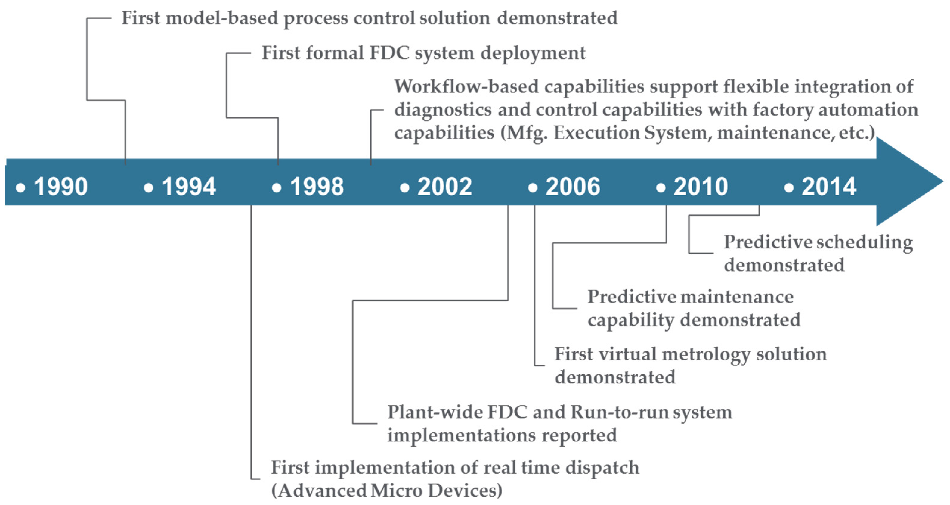
Figure 1. History of process analytics in semiconductor manufacturing. Dates are approximate and determined from an analysis of publications in Advanced Process Control Conferences, with permission from [6,12], Copyright Advanced Process Control Conferences 2016.
Processes 05 00039 g001
Figure 2. The big data explosion in semiconductor manufacturing, presented in [17], with permission from [17]. Copyright Advanced Process Control Conference, 2016. The different colors refer to the primary process types in the semiconductor “fab”, namely etch, lithography, deposition, defect inspection and other metrology, and others.
Processes 05 00039 g002
Figure 3. Dimensions of analytics capabilities with mapping of typical advanced process control (APC) solutions in semiconductor manufacturing to these dimensions.
Processes 05 00039 g003
Figure 4. Effective anomaly detection in semiconductor manufacturing today using univariate end-of-run trace data analysis, feature extraction, and limits monitoring, leveraging subject matter expertise (SME).
Processes 05 00039 g004
Figure 5. Semi-automated trace partitioning in which patterns of interest are defined (left); and then each sensor trace is partitioned along the boundaries of each of these patterns (right).
Processes 05 00039 g005
Figure 6. Results of applying fault detection and classification (FDC) with semi-automated trace partitioning and feature extraction.
Processes 05 00039 g006
Figure 7. Usage of receive operating characteristic (ROC) plots to determine optimal fault detection (FD) limits settings; plot of true/false positive rates as a function of FD limits settings.
Processes 05 00039 g007
Figure 8. The approach to predictive maintenance: (a) the multivariate analysis (MVA) predictor and its components including time-to-failure horizon and some expression of prediction confidence or range; and (b) the off-line model building and optimization approach that provides a mechanism for incorporating subject matter expertise (SME), and can be leveraged for many advanced process control (APC) predictive capabilities.
Processes 05 00039 g008
Figure 9. Illustration of epitaxial process lamp replacement predictive maintenance (PdM).
Processes 05 00039 g009
Figure 10. A smart manufacturing vision depiction for semiconductor manufacturing, with permission from [17]. Copyright Advanced Process Control Conference, 2016.
Processes 05 00039 g010
Table 1. Definitions of Advanced Process Control (APC) and APC extended capabilities.
TechnologyDefinition
Advanced Process Control (APC)The manufacturing discipline for applying control strategies and/or employing analysis and computation mechanisms to recommend optimized machine settings and detect faults and determine their cause.
APC Base Technologies as Defined in [24]
Fault Detection (FD)The technique of monitoring and analyzing variations in tool and/or process data to detect anomalies. FD includes both univariate (UVA) and multivariate (MVA) statistical analysis techniques.
Fault Classification (FC)The technique of determining the cause of a fault once it has been detected.
Fault Detection and Classification (FDC)A combination of FD and FC.
Fault Prediction (or prognosis) (FP)The technique of monitoring and analyzing variations in process data to predict anomalies.
Run-to-Run (R2R) ControlThe technique of modifying recipe parameters or the selection of control parameters between runs to improve processing performance. A “run” can be a batch, lot, or an individual wafer.
Statistical Process Control (SPC)The technique of using statistical methods to analyze process or product metrics to take appropriate actions to achieve and maintain a state of statistical control and continuously improve the process capability.
APC Extended Technologies as Defined in [19,20]
Equipment Health Monitoring (EHM)The technology of monitoring tool parameters to assess the tool health as a function of deviation from normal behavior. EHM is not necessarily predictive in nature, but is often a component of predictive systems.
Predictive Maintenance (PdM)The technology of utilizing process and equipment state information to predict when a tool or a particular component in a tool might need maintenance, and then utilizing this prediction as information to improve maintenance procedures. This could mean predicting and avoiding unplanned downtimes and/or relaxing un-planned downtime schedules by replacing schedules with predictions. PdM solutions as defined herein address the entire maintenance cycle, from predicting maintenance through addressing recovery from maintenance events towards returning to production.
Predictive SchedulingThe technology of utilizing current and projected future information on tool and factory state, capabilities, WIP, schedule, dispatch and orders to predict and improve scheduling of a system (tool, group of tools, fab, etc.).
Virtual Metrology (VM)The technology of prediction of post process metrology variables (either measurable or not measurable) using process and wafer state information that could include upstream metrology and/or sensor data. Terms such as virtual sensing and sensor fusion have also been used to represent this capability.
Yield PredictionThe technology of monitoring information across the fab (e.g., tool and metrology) to predict process or end of line yield.