Fabrication of New Liquid Crystal Device Using Layer-by-Layer Thin Film Process
by
 and
and
Gitae Moon
1,†, 
Wonjun Jang
2,†,
Intae Son
1,
Hyun A. Cho
2,
Yong Tae Park
2,* and
Jun Hyup Lee
1,* 1
Department of Chemical Engineering, Myongji University, Yongin, Gyeonggi 17058, Korea
2
Department of Mechanical Engineering, Myongji University, Yongin, Gyeonggi 17058, Korea
*
Authors to whom correspondence should be addressed.
†
These authors contributed equally to this work.
Processes 2018, 6(8), 108; https://doi.org/10.3390/pr6080108
Submission received: 29 June 2018
/
Revised: 20 July 2018
/
Accepted: 26 July 2018
/
Published: 1 August 2018
(This article belongs to the Special Issue Thin Film Processes)
Abstract
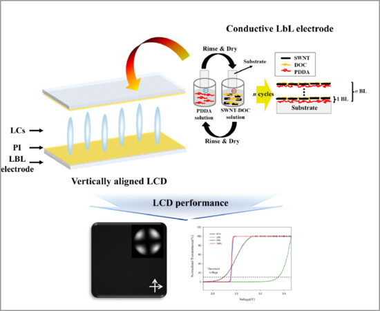
:Indium tin oxide (ITO) transparent electrodes are troubled with high cost and poor mechanical stability. In this study, layer-by-layer (LBL)-processed thin films with single-walled carbon nanotubes (SWNTs) exhibited high transparency and electrical conductivity as a candidate for ITO replacement. The repetitive deposition of polycations and stabilized SWNTs with a negative surfactant exhibits sufficiently linear film growth and high optoelectronic performance to be used as transparent electrodes for vertically aligned (VA) liquid crystal display (LCD) cells. The LC molecules were uniformly aligned on the all of the prepared LBL electrodes. VA LCD cells with SWNT LBL electrodes exhibited voltage-transmittance (V-T) characteristics similar to those with the conventional ITO electrodes. Although the response speeds were slower than the LCD cell with the ITO electrode, as the SWNT layers increased, the display performance was closer to the LCD cells with conventional ITO electrode. This work demonstrated the good optoelectronic performance and alignment compatibility with LC molecules of the SWNT LBL assemblies, which are potential alternatives to ITO films as transparent electrodes for LCDs.
1. Introduction
Liquid crystal displays (LCDs) are extensively utilized in daily life for items such as notebook computers, smartphones, and portable televisions due to their lightweight, low power consumption, and good mobility. Up to the present day, many studies have revealed several LC modes of display to achieve high picture qualities, e.g., in-plane switching (IPS) [1], pixel-patterned vertical alignment (VA) [2], and fringe-field switching (FFS) [3]. In an LCD, LC molecules located between two electrodes are moved by the applied electric field to transmit light, thereby displaying information.
Because of the growing interest in display applications, many studies on transparent electrodes have been recently conducted, focusing on electron transport and high transparency. In previous studies, metal oxides have been investigated as transparent electrodes because they display low resistance and high transparency [4,5]. Indium tin oxide (ITO) material has been commonly used for the last several decades as a transparent electrode thin film owing to its high visible transparency, excellent electrical conductivity, and availability of deposition on glass and plastic substrates. However, its high production cost and fragile characteristics limit its applicability for flexible electronic devices [6,7]. Also, the total reflection at the glass/ITO interface and the low adhesion to organic substrates lower the display performance of LC devices containing ITO transparent electrodes [8,9]. Many electrode materials, such as organic carbon nanotubes (CNTs) [10,11], metallic nanowires [12,13], metal thin films [14], graphene [15,16], and conductive polymers [17,18], have been studied as alternatives to ITO.
The single-walled carbon nanotube (SWNT) with a few nanometer radius is an emerging and especially promising material as alternative transparent electrodes. Several approaches have been utilized to generate SWNT films such as transfer printing [19], direct chemical vapor deposition (CVD) growth [20], vacuum filtration [21], and rod coating [22]. These SWNT thin films showed fairly high optical transmittance and good conducting properties which are similar to those of the conventional ITO-coated poly(ethylene terephthalate) (PET; 50–200 Ω resistance and ~83% transmission at 550 nm) substrate [23]. However, these methods tend to exhibit some problems such as poor film surface, optoelectronic performance, high cost, and a complex process [24]. Transfer printing, one of the most-used thin film techniques, results in difficult large-area fabrication and relatively brittle SWNT thin films. Therefore, in this study, we focused on the transparent electrode properties of SWNT by the layer-by-layer (LBL) process. Compared with other CNT thin film methods, the LBL technique provides the precise control needed to make thin films with a few nanometer thickness.
LBL assembly is one of the wet coating methods that has been widely studied in last 20 years due to its simple process and high controllability under ambient conditions [25,26]. This process can be used as a method of producing the thin films suitable for a variety of materials, which may include nanoparticles, nanotubes, nanowires, nanoplatelets, dyes, dendrimers, proteins, and viruses. The LBL process enables the production of homogeneous multifunctional multilayers with a controlled method. Moreover, it can be applied to a variety of substrates (e.g., glass and quartz slides, silicon wafers, and polymeric films) to evaluate the performance of electrical conductivity [27,28], sensing [29,30], and energy harvesting [31].
In this study, VA LCD devices with a polyimide (PI) alignment layer on SWNTs and poly (diallyldimethylammonium chloride) (PDDA) layer-by-layer electrodes were fabricated and characterized to evaluate their potential for transparent organic electrode materials in an LC display. Firstly, PDDA was used as the positively charged polyelectrolyte in conjunction with a negatively charged surfactant to deposit SWNTs onto a PDDA layer. The alternate dipping in positively and negatively charged solutions resulted in SWNT/polymer thin film deposition onto the substrate. The LC test devices were fabricated by filling the LCs into the inner parts of the PI layer by spin coating, and their device structures have been reported in the literature [32,33]. The electro-optical (E-O) properties of the prepared VA LCD devices containing the LBL transparent electrodes were examined and compared to those of LCD devices with conventional ITO electrodes.
2. Materials and Methods
2.1. Materials
Purified electric arc SWNTs (TUBALL™ SWNT, individual tube: average 1 μm length and 2 nm diameter, C > 75%) were used in this study. PDDA (Mw ~200,000–350,000 g/mol), sodium deoxycholate (DOC, C24H39NaO4), isopropyl alcohol (IPA), and methanol were purchased from Sigma-Aldrich (Yongin, Korea). Nematic LCs (∆n = 0.095, ∆ε = −3.1), PI (AL607XX, JSR, Tokyo, Japan), ITO glass (SNT 15Ω, FINE CHEMICAL, Seoul, Korea), UV-curable sealant (SD-2X, Sekisui Chemical, Tokyo, Japan), and ball spacers with a diameter of 3.25 μm (SP-205XX, Sekisui Chemical, Tokyo, Japan) were used to fabricate the LCD. All chemicals were used as received. Slide glasses, PET films (100 μm thickness, Goodfellow, Huntingdon, England), and quartz crystals with 5 MHz gold-electrodes (Maxtek, Inficon Korea, Seongnam, Korea) were purchased for analysis of UV–Visible (UV–Vis) light absorbance, field emission scanning electron microscopy (FE-SEM), and mass, respectively.
2.2. Fabrication of LCD Cells Using SWNT LBL Transparent Electrodes
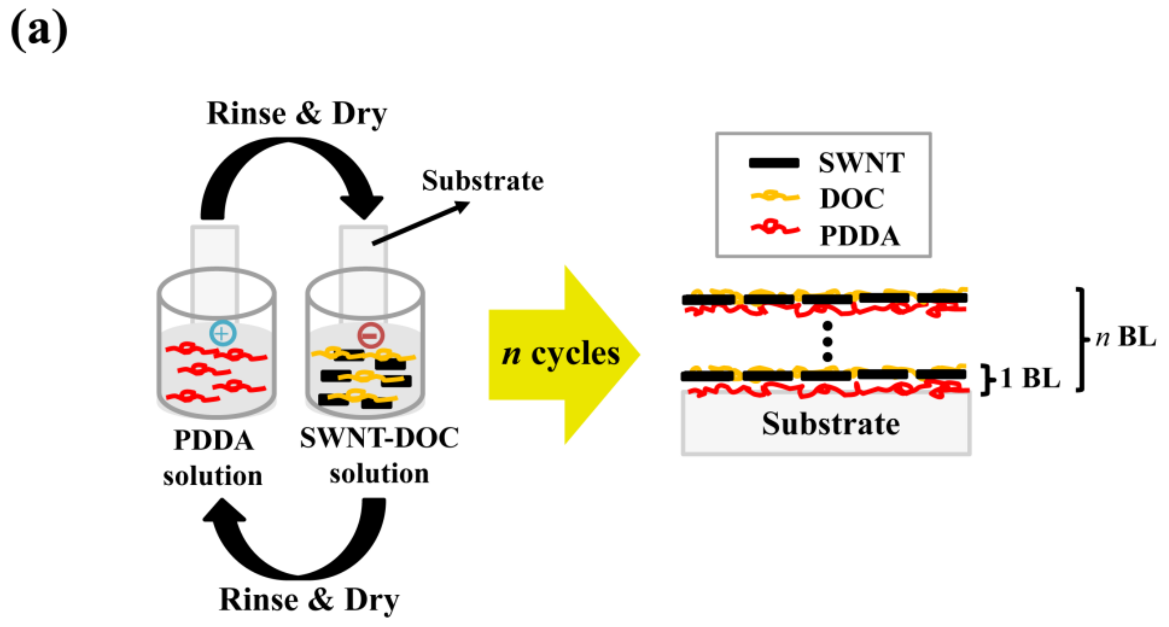
Both positively and negatively charged aqueous solutions were obtained by using 18.2 MΩ deionized (DI) water (YL aquaMAX Ultra 370, YL Instrument, Anyang, Korea). A PDDA solution with a concentration of 0.25 wt. % as a cationic solution was prepared. An SWNT dispersion (0.05 wt. %) treated by 1.5 wt. % DOC in DI water (SWNT–DOC dispersion) was prepared as a negatively charged solution. The large SWNT bundles in the SWNT–DOC dispersion were removed by tip ultrasonication (HD-1070, Sonopuls, Berlin, Germany) for 45 min. Then, each surface of the slide glasses was cleaned by a plasma treatment (PDC 32G-2, Harrick Plasma, Ithaca, NY, USA) for 10 min. The PET films were cleaned with IPA, methanol, and DI water, dried thoroughly with clean air, and then also treated by the plasma etcher for 5 min. For LBL deposition, PET films and glass slides were alternately dipped into PDDA and SWNT–DOC solutions with rinsing and drying, beginning with the PDDA. Each deposition cycle resulted in one bilayer (BL) on the substrate. For the cyclic deposition, the PDDA and SWNT–DOC layers were formed by 5 min of dipping for each, followed by rinsing and drying. The schematic representation of the LBL thin film process is shown in Figure 1a. The notation of [PDDA/(SWNT–DOC)]n (n = the number of BLs on the substrate) represents the deposition cycle of LBL thin films. Light absorbance was measured between 400 and 800 nm and transmittance was calculated from the absorbance measured by a UV–Vis spectrometer (USB2000, Ocean Optics, Wonwoo Systems, Seoul, Korea). The mass growth from the LBL deposition was measured by a quartz crystal microbalance (QCM, QCM 200, Standard Research System, Inficon Korea, Seongnam, Korea). Sheet resistance was measured with a digital multimeter (Model2000, Keithley, Seoul, Korea). Surface images of LBL thin films were acquired with a FE-SEM (SU-70, Hitachi High-Technologies, Seoul, Korea) at the voltage of 15 kV.
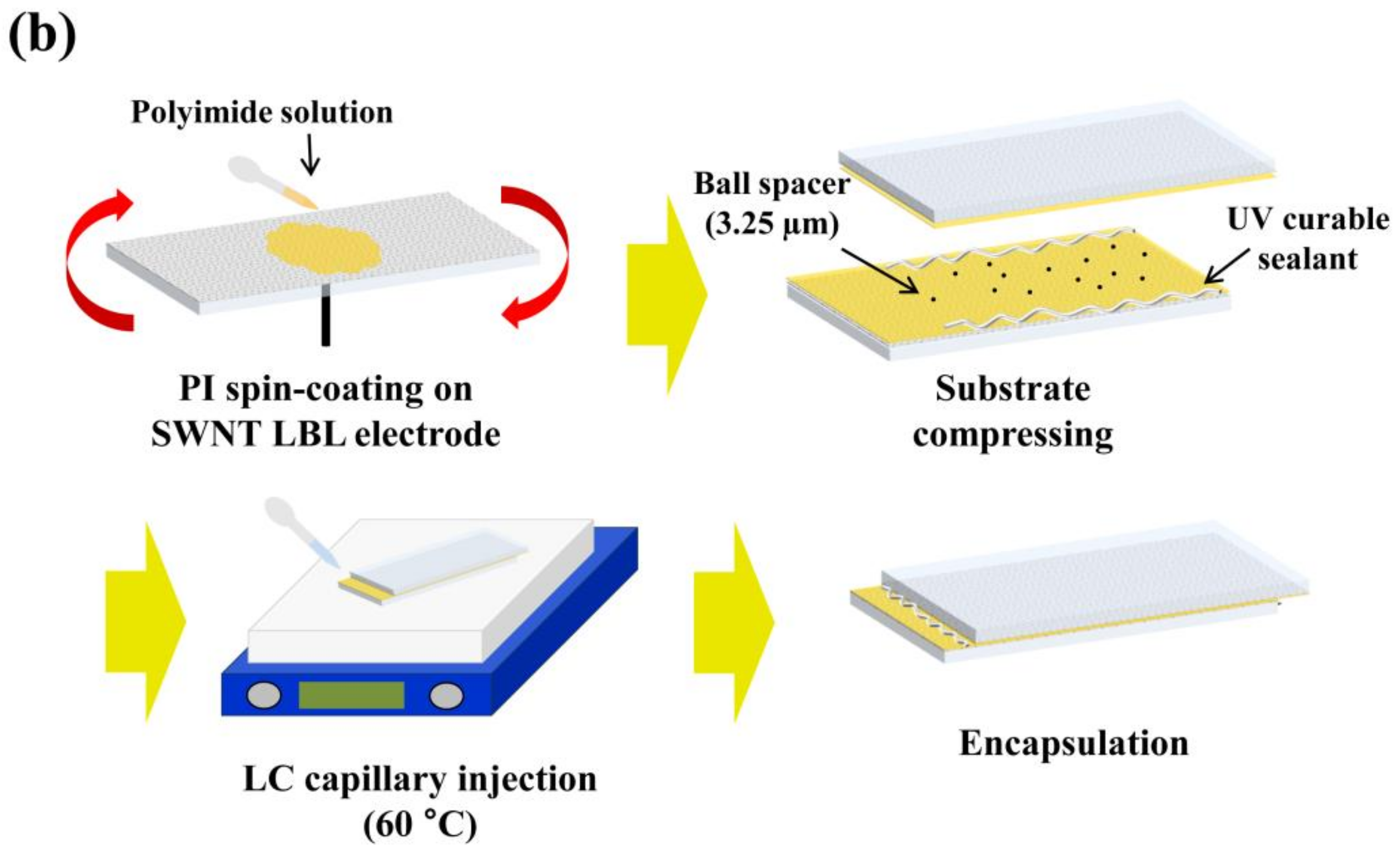
The overall process for manufacturing the LCD using the transparent SWNT-based electrode fabricated by the LBL method is shown in Figure 1b. PI was uniformly coated on the LBL film at 3500 rpm for 30 s to form alignment layers. These PI layers on the LBL film were imidized at 230 °C for 30 min. The LBL-LCD cell was manufactured by coupling the two LBL substrates. The cell gap of the LBL-LCD device was formed by using 3.25-μm ball spacers. The ball spacers were dispersed in an ethanol solution and then sprayed on the PI-coated LBL electrode. An empty cell for LC injection was prepared by applying the UV-curable sealant on the PI-coated substrate and then attaching the upper and lower substrates together. The sealant was cured by exposure to UV radiation of 3.0 J∙cm−2 (WUV-L50, DAIHAN, Seoul, Korea). After the empty LBL-LCD cell was filled with nematic LCs at 60 °C using capillary force, the inlet and outlet areas were sealed using the UV-curable sealant. The manufactured LBL-LCD cell was thermally treated for 1 h at 100 °C. The LC alignment was examined by a polarized optical microscope (POM; BX51, OLYMPUS, Tokyo, Japan) with a crossed polarizer. To evaluate the E-O characteristics, the voltage-transmittance (V-T) curve and on/off response time of the LCD cell were investigated. Further, to investigate the E-O properties according to the number of bilayers, the PI layer was spin coated on 2, 6, and 10 BLs electrodes to fabricate LCD cells with different configurations.
3. Results and Discussion
Figure 2 shows the image of 2–10 BLs SWNT LBL thin films deposited on the glass substrates, the SEM surface image of these PDDA/SWNT LBL assemblies on the PET substrate, and a photograph of the prepared LC cell using an SWNT LBL electrode. The growth of SWNT deposition was observed as the increase in the number of BLs deposited and was confirmed using QCM mass and UV–Vis absorbance measurements, as shown in Figure 3. In a SEM image of Figure 2b, the LBL thin film with 10 BLs exhibits a good distribution of SWNTs owing to the exfoliation of individual SWNTs in water by DOC [27,28]. The dispersion of SWNTs provides the contacts within the nanotube network, indicating a transport route of electrons through the film. Also, SWNT LBL deposition was quite uniform. SWNT–DOCs are uniformly deposited onto the PDDA layer and the following PDDA deposits are thick enough to lead to the smooth surface of thin film.
Figure 3 shows the absorbance spectra of the SWNT LBL thin films from 1 to 10 BLs at wavelengths between 450 and 800 nm and the mass growth curve of the LBL thin films corresponding to the number of bilayers deposited. Because the absorbance of UV–Vis light increases in proportion to the thickness of thin films, Figure 3a exhibits the almost linear growth of LBL multilayers (i.e., PDDA and SWNT–DOC BLs) up to 10 BLs. Moreover, the Table 1 shows that the transparency decreases with increasing BLs in the visible light wavelength, suggesting that the SWNT is coated proportionally as BLs are deposited. As the number of BLs increases, the electrical conductivity decreases because the amount of SWNTs coated on the glass slide increases proportionally. Similar to the UV–Vis absorbance, the mass of [PDDA/(SWNT–DOC)]n measured by QCM in Figure 3b shows a quite linear increase with the number of BLs, suggesting constant deposition up to 10 BLs.
Figure 4 is a graph showing the optoelectronic relationship of the LBL thin films by showing electric resistance as a function of optical transparency. Both resistance and transparency decreased as the number of BLs increased. In the previous studies, the thicker SWNT films showed the higher conductivity due to a more three-dimensional SWNT network [27,28]. For the reason of more efficient electron transport, the resistance of LBL electrodes decreases according to the number of BLs. The amount of SWNTs coated on the substrate increases along with the number of BLs, so the optical transparency decreases. The electrical and optical properties of some SWNT LBL electrodes used for LCD cells are also summarized and compared with ITO in Table 1. Despite the relatively low resistance of 1 kΩ at high BLs, it should be even lower for a reasonable ITO replacement.
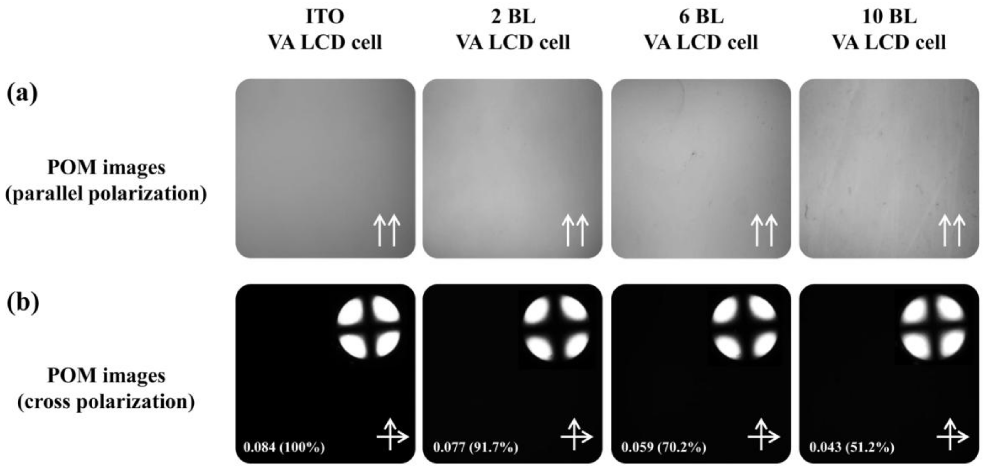
The POM photographs of the VA LCDs with the crossed polarizer set in two orientations with respect to the LCD cells are shown in Figure 5. Figure 5a exhibits the image of the LCD cell with the polarizer in the same direction as the cell. The LCD cell using the LBL electrode exhibited almost the same image as the LCD cell using the ITO substrate. However, as the number of BLs increased, the LCD cell showed a very fine texture. The LCD cell using the 2 BL SWNT electrode showed no heterogeneity, and the LCD cell using the 10 BL electrode showed a fine texture, probably due to impurities incorporated in the LBL process. Figure 5b shows the image of the LCD cell under cross polarization. The LCD cell using the LBL electrode exhibited a nearly uniform black image, similar to that exhibited by the cell using the ITO substrate. Moreover, the slight heterogeneity in polarizers in the same direction was not observed at all in the black images. Under cross polarization, the VA LCD cells with LBL electrodes showed lower transmittances than the cell with ITO electrodes. While VA LCD cells with ITO showed a transmittance of 0.084 (100%), VA LCD cells with LBL electrodes exhibited 0.077 (91.7%), 0.059 (70.2%), and 0.043 (51.2%) for 2 BL, 6 BL, and 10 BL, respectively. These results indicated the creation of uniform homeotropic LC alignment on the LBL thin film electrode; the number of BLs did not disturb the vertical alignment of the nematic LCs in the device. In addition, typical conoscopic images of the VA LCDs are shown in the insets of Figure 5 [34,35]. The conoscopic images showed a distinct Maltese cross, which indicates the vertical alignment of the LC molecules.
To confirm the effect of the number of BLs, we measured the V-T characteristics and response time properties of the newly manufactured LCDs, which represented their E-O properties. The voltage-dependent optical transmittance of the VA LCDs is shown in Figure 6. The shapes of the V-T curves of VA LCD cells using the SWNT LBL electrodes in the transmittance range of 10%–90% were similar to those of conventional VA LCD cells using the ITO electrode. In the V-T curves, threshold voltages at a transmittance of 10% were 3.34, 2.38, 2.34, and 2.23 V for cells with the 2-BL, 6-BL, 10-BL, and ITO electrodes, respectively. It is noteworthy that the threshold voltage of the VA LCD cells containing the LBL electrode was higher than that of the LC device with the conventional ITO electrode. This means that the LC molecules form a stable vertical alignment similar to that using the ITO electrode. However, the 2-BL electrode showed the highest threshold voltage of 3.34 V. This result suggests that the high resistance due to the small SWNT layers causes the LC molecules to drive at a high voltage. As the number of BLs increased, the electrical resistance decreased, and the threshold voltage tended towards values closer to that of the LCD cell using the conventional ITO electrode. Particularly noteworthy is the fact that the driving voltage of LCD cells with 6 BLs or 10 BLs is lower than that of LCD cells with ITO electrodes. While the LC device with ITO showed a white state at 2.8 V, the LCD containing 6 BLs or 10 BLs exhibited an on-state at 2.4 V. As a result, it was confirmed that there is no problem in driving the LC device with 6 BLs or more SWNT layers.
We confirmed the switching drive of the LCDs by measuring the response time of the newly manufactured LCD cell. The response time characteristics were confirmed by measuring the transmittance caused by the alignment change of the LC molecules by applying a square wave of 120 Hz to the LCD cell using a waveform generator. Figure 7a exhibits the rising time curves of the LCDs fabricated with the ITO and SWNT LBL electrodes, and Figure 7b shows their falling time curves. The LCD cell using the LBL electrode could be switched on or off by applying voltage, similar to the cell using the conventional ITO substrate. However, due to the high electrical resistance of the LBL thin film, a time delay occurred until the square wave was actually applied. Due to this time delay, the response characteristics of the LCD cell using the LBL electrode was slower than that of the LC device with the conventional ITO electrode. The VA LCD cells manufactured using the conventional ITO electrode had a rising time of 22 ms and a falling time of 15 ms. The VA LCD cell using the 10-BL electrode had on and off times of 100 ms and 106 ms, respectively, because it had the lowest electrical resistance among the LBL electrodes. The VA LCD cell using the 6-BL electrode had rising and fall times of 139 ms and 152 ms, respectively. The fabricated VA LCD cell using the 2-BL electrode had a 201 ms on time and a 209 ms off time. Thus, it was confirmed that the response time of the prepared LC device using the LBL electrode was slower than that using the conventional ITO electrode, but the response time became closer to that of the ITO electrode as the number of BLs increased.
4. Conclusions
In this study, transparent electrodes for LCDs were fabricated with SWNT thin films by the LBL method to replace conventional ITO electrodes. SWNT LBL films with lower than 1.3 kΩ of electrical resistance and greater than 85% of optical transparency were fabricated by repetitive immersion of the substrate into positively and negatively charged polyelectrolyte solutions. The nematic LCs were uniformly aligned by spin coating a VA PI film on the prepared LBL electrode. The POM images of the VA LCD cell using the LBL electrode confirmed that the LC molecules were uniformly aligned. Moreover, the number of bilayers did not influence the homeotropic alignment of the nematic LC materials. Also, LCD cells using the proposed electrode exhibited V-T characteristics similar to that of VA LCD cells using the conventional ITO electrode, with its on/off state depending on the application of voltage. Due to the high electrical resistance of the LBL electrode, the response speed characteristics of the LCD device using the LBL electrode were slower than that of the LC display using the conventional ITO electrode. However, as the number of BLs increased, the threshold voltage and response time tended to be closer to that of the ITO electrode and the response speed became faster. These results demonstrated the potential of the LBL thin films as good alternatives to ITO films as transparent conducting electrodes for LCDs. The combination of simple processing and good optoelectronic performance should make SWNT LBL thin films very promising for future display applications.
Author Contributions
G.M., Y.T.P., and J.H.L. conceptualized the phenomenon. Y.T.P. and J.H.L. designed the project. G.M., W.J., I.S., and H.A.C. conducted the experiments. All authors wrote the manuscript and analyzed the data. Y.T.P. and J.H.L. supervised the whole project.
Funding
This work was financially supported by the Mid-career Researcher Program (No. 2017R1A2B4006104) through a National Research Foundation of Korea (NRF) grant funded by the Ministry of Science, ICT and Future Planning (MSIP). This work was also supported by the National Research Foundation of Korea (NRF) grant funded by the Korea government (MSIT) (No. NRF-2018R1A5A1024127).
Conflicts of Interest
The authors declare no conflict of interest. The funders had no role in the design of the study; in the collection, analyses, or interpretation of data; in the writing of the manuscript, and in the decision to publish the results.
Nomenclature
| BL | Bilayer |
| CNT | Carbon nanotube |
| CVD | Chemical vapor deposition |
| DI | Deionized, DOC: Sodium deoxycholate |
| E-O | Electro-optical |
| FE-SEM | Field emission scanning electron microscopy |
| FFS | Fringe-field switching |
| IPA | Isopropylalcohol |
| IPS | In-plane switching |
| ITO | Indium tin oxide |
| LBL | layer-by-layer |
| LCD | Liquid crystal display |
| PDDA | Poly(diallyldimethylammonium chloride) |
| PET | Poly(ethylene terephthalate) |
| PI | Polyimide |
| POM | Polarized optical microscope |
| QCM | Quartz crystal microbalance |
| SWNT | Single-walled carbon nanotube |
| TNI | Nematic-to-isotropic transition temperature |
| UV–Vis | UV–Visible spectroscopy |
| VA | Vertical alignment |
| V-T | Voltage-transmittance |
References
- Ohe, M.H.; Kondo, K.S. Electro-optical characteristics and switching behavior of the in-plane switching mode. Appl. Phys. Lett. 1995, 67, 3895–3897. [Google Scholar] [CrossRef]
- Lee, Y.J.; Kim, Y.K.; Jo, S.I.; Bae, K.S.; Choi, B.D.; Kim, J.H.; Yu, C.J. Fast vertical alignment mode with continuous multi-domains for a liquid crystal display. Opt. Express 2009, 17, 23417–23422. [Google Scholar] [CrossRef] [PubMed]
- Lee, S.H.; Lee, S.L.; Kim, H.Y. Electro-optic characteristics and switching principle of a nematic liquid crystal cell controlled by fringe-field switching. Appl. Phys. 1998, 73, 2881–2883. [Google Scholar] [CrossRef]
- Igasaki, Y.; Saito, H. Substrate temperature dependence of electrical properties of ZnO:Al epitaxial films on sapphire. J. Appl. Phys. 1991, 69, 2190–2195. [Google Scholar] [CrossRef]
- Lan, Y.F.; Peng, W.C.; Lo, Y.H.; He, J.L. Indium tin oxide films deposited by thermionic-enhanced DC magnetron sputtering on unheated polyethylene terephthalate polymer substrate. Mater. Res. Bull. 2009, 44, 1760–1764. [Google Scholar] [CrossRef]
- Lin, Y.C.; Shi, W.Q.; Chen, Z.Z. Effect of deflection on the mechanical and optoelectronic properties of indium tin oxide films deposited on polyethylene terephthalate substrates by pulse magnetron sputtering. Thin Solid Films 2009, 517, 1701–1705. [Google Scholar] [CrossRef]
- Gu, G.; Shen, Z.; Burrows, P.E.; Forrest, S.R. Transparent flexible organic light-emitting devices. Adv. Mater. 1997, 9, 725–728. [Google Scholar] [CrossRef]
- Cairns, D.R.; Witte, R.P.; Sparacin, D.K.; Sachsman, S.M.; Paine, D.C.; Crawford, G.P.; Newton, R.P. Strain-dependent electrical resistance of tin-doped indium oxide on polymer substrates. Appl. Phys. Lett. 2000, 76, 1425–1427. [Google Scholar] [CrossRef]
- Tao, C.S.; Jiang, J.; Tao, M. Natural resource limitations to terawatt-scale solar cells. Sol. Energy Mater. Sol. Cells 2011, 95, 3176–3180. [Google Scholar] [CrossRef]
- Wu, Z.; Chen, Z.; Du, X.; Logan, J.M.; Sippel, J.; Nikolou, M.; Kamaras, K.; Reynolds, J.R.; Tanner, D.B.; Hebard, A.F.; et al. Transparent, conductive carbon nanotube films. Science 2004, 305, 1273–1276. [Google Scholar] [CrossRef] [PubMed]
- Zhang, M.; Fang, S.; Zakhidov, A.A.; Lee, S.B.; Aliev, A.E.; Williams, C.D.; Atkinson, K.R.; Baughman, R.H. Strong, transparent, multifunctional, carbon nanotube sheets. Science 2005, 309, 1215–1219. [Google Scholar] [CrossRef] [PubMed]
- Lee, J.Y.; Connor, S.T.; Cui, Y.; Peumans, P. Solution-Processed Metal Nanowire Mesh Transparent Electrodes. Nano Lett. 2008, 8, 689–692. [Google Scholar] [CrossRef] [PubMed] [Green Version]
- Hsu, P.C.; Wang, S.; Wu, H.; Narasimhan, V.K.; Kong, D.; Lee, H.R.; Cui, Y. Performance enhancement of metal nanowire transparent conducting electrodes by mesoscale metal wires. Nat. Commun. 2013, 25, 2522–2528. [Google Scholar] [CrossRef] [PubMed]
- Meiss, J.; Riede, M.K.; Leo, K. Optimizing the morphology of metal multilayer films for indium tin oxide (ITO)-free inverted organic solar cells. Appl. Phys. Lett. 2009, 105, 063108-1–063108-5. [Google Scholar] [CrossRef]
- Tung, V.C.; Chen, L.M.; Allen, M.J.; Wassei, J.K.; Nelson, K.; Kaner, R.B.; Yang, Y. Low-temperature solution processing of graphene-carbon nanotube hybrid materials for high-performance transparent conductors. Nano Lett. 2009, 9, 1949–1955. [Google Scholar] [CrossRef] [PubMed]
- Mei, X.G.; Ouyang, J.Y. Ultrasonication-assisted ultrafast reduction of graphene oxide by zinc powder at room temperature. Carbon 2011, 49, 5389–5397. [Google Scholar] [CrossRef]
- Alemu, D.L.; Wei, H.Y.; Ho, K.C.; Chu, C.W. Highly conductive PEDOT:PSS electrode by simple film treatment with methanol for ITO-free polymer solar cells. Energy Environ. Sci. 2012, 5, 9662–9671. [Google Scholar] [CrossRef]
- Na, S.I.; Kim, S.S.; Jo, J.; Kim, D.Y. Efficient and Flexible ITO-Free Organic Solar Cells Using Highly Conductive Polymer Anodes. Adv. Mater. 2008, 21, 4061–4067. [Google Scholar] [CrossRef]
- Zhang, D.; Ryu, K.; Liu, X.; Polikarpov, E.; Ly, J.; Tompson, M.E.; Zhou, C. Transparent, conductive, and flexible carbon nanotube films and their application in organic light-emitting diodes. Nano Lett. 2006, 6, 1880–1886. [Google Scholar] [CrossRef] [PubMed]
- Ma, W.; Song, L.; Yang, R.; Zhang, T.; Zhao, Y.; Sun, L.; Zhang, Z. Directly synthesized strong, highly conducting, transparent single-walled carbon nanotube films. Nano Lett. 2007, 7, 2307–2311. [Google Scholar] [CrossRef] [PubMed]
- Green, A.A.; Hersam, M.C. Colored Semitransparent Conductive Coatings Consisting of Monodisperse Metallic Single-Walled Carbon Nanotubes. Nano Lett. 2008, 8, 1417–1422. [Google Scholar] [CrossRef] [PubMed]
- Dan, B.; Irvin, G.C.; Pasquali, M. Continuous and scalable fabrication of transparent conducting carbon nanotube films. ACS Nano 2009, 3, 835–843. [Google Scholar] [CrossRef] [PubMed]
- Park, Y.T.; Ham, A.Y.; Yang, Y.H.; Grunlan, J.C. Fully organic ITO replacement through acid doping of double-walled carbon nanotube thin film assemblies. RSC Adv. 2011, 1, 662–671. [Google Scholar] [CrossRef]
- Yu, X.; Rajamani, R.; Stelson, K.A.; Cui, T. Fabrication of carbon nanotube based transparent conductive thin films using layer-by-layer technology. Surf. Coat. Technol. 2008, 202, 2002–2007. [Google Scholar] [CrossRef]
- Decher, G.; Lvov, Y.; Schmitt, J. Proof of multilayer structural organization in self-assembled polycation-polyanion molecular films. Thin Solid Films 1994, 244, 772–777. [Google Scholar] [CrossRef]
- Hammond, P.T. Form and function in multilayer assembly: New applications at the nanoscale. Adv. Mater. 2004, 16, 1271–1293. [Google Scholar] [CrossRef]
- Park, Y.T.; Ham, A.Y.; Grunlan, J.C. High electrical conductivity and transparency in deoxycholate-stabilized carbon nanotube thin films. J. Phys. Chem. C 2010, 114, 6325–6333. [Google Scholar] [CrossRef]
- Park, Y.T.; Ham, A.Y.; Grunlan, J.C. Heating and acid doping thin film carbon nanotube assemblies for high transparency and low sheet resistance. J. Mater. Chem. 2011, 21, 363–368. [Google Scholar] [CrossRef]
- Park, J.J.; Hyun, W.J.; Mun, S.C.; Park, Y.T.; Park, O.O. Highly stretchable and wearable graphene strain sensors with controllable sensitivity for human motion monitoring. ACS Appl. Mater. Interfaces 2015, 7, 6317–6324. [Google Scholar] [CrossRef] [PubMed]
- Zhou, M.; Dong, S. Bioelectrochemical interface engineering: Toward the fabrication of electrochemical biosensors, biofuel cells, and self-powered logic biosensors. Accounts Chem. Res. 2011, 44, 1232–1243. [Google Scholar] [CrossRef] [PubMed]
- Chung, I.J.; Kim, W.; Jang, W.; Park, H.W.; Sohn, A.; Chung, K.B.; Kim, D.W.; Choi, D.; Park, Y.T. Layer-by-layer assembled graphene multilayers on multidimensional surfaces for highly durable, scalable, and wearable triboelectric nanogenerators. J. Mater. Chem. A 2018, 6, 3108–3115. [Google Scholar] [CrossRef]
- Wang, H.Y.; Wu, T.X.; Zhu, X.Y.; Wu, S.T. Correlations between liquid crystal director reorientation and optical response time of a homeotropic cell. J. Appl. Phys. 2004, 95, 5502–5508. [Google Scholar] [CrossRef]
- Seo, D.S.; Kim, J.H. Generation of pretilt angle in NLC and EO characteristics of transcription-aligned TNLCD fabricated by transcription alignment on polyimide surfaces. Liq. Cryst. 1999, 26, 397–400. [Google Scholar] [CrossRef]
- Kim, T.H.; Ju, C.H.; Kang, H. Vertical alignment of liquid crystal on tocopherol substituted polystyrene films. Liq. Cryst. 2018, 45, 801–810. [Google Scholar] [CrossRef]
- Oh, S.K.; Nakagawa, M.S.; Ichimura, K.H. Relationship between the ability to control liquid crystal alignment and wetting properties of calix[4]resorcinarene monolayers. J. Mater. Chem. 2001, 11, 1563–1569. [Google Scholar] [CrossRef]
Figure 1.
(a) Schematic illustration of the layer-by-layer (LBL) dipping process with poly (diallyldimethylammonium chloride) (PDDA) and single-walled carbon nanotube–sodium deoxycholate (SWNT–DOC) aqueous solutions. (b) Manufacturing process of liquid crystal display (LCD) using transparent SWNT electrode fabricated by the LBL method.


Figure 2.
(a) Photograph of [PDDA/(SWNT–DOC)]n (n = 2–10) assemblies on both sides of a glass slide. (b) SEM surface image of [PDDA/(SWNT–DOC)]10 on a poly(ethylene terephthalate) (PET) film. (c) Photograph of an LC cell using an SWNT LBL electrode.
Figure 2.
(a) Photograph of [PDDA/(SWNT–DOC)]n (n = 2–10) assemblies on both sides of a glass slide. (b) SEM surface image of [PDDA/(SWNT–DOC)]10 on a poly(ethylene terephthalate) (PET) film. (c) Photograph of an LC cell using an SWNT LBL electrode.

Figure 3.
(a) UV–Visible (UV–Vis) absorbance spectra of [PDDA/(SWNT–DOC)]n (n = 1–10) thin films and an indium tin oxide (ITO) coating from 450 to 800 nm wavelength. (b) Light absorbance and transmittance (inset) of 1–10 bilayers (BLs) at 550 nm wavelength. (c) Mass growth of a [PDDA/(SWNT–DOC)] system up to 14 BLs (half BL:PDDA deposition).

Figure 4.
Optoelectronic performance (electrical resistance vs. optical transmittance at 550 nm wavelength) of [PDDA/(SWNT–DOC)]n thin films as a function of the number of bilayers deposited to 10 BLs.
Figure 4.
Optoelectronic performance (electrical resistance vs. optical transmittance at 550 nm wavelength) of [PDDA/(SWNT–DOC)]n thin films as a function of the number of bilayers deposited to 10 BLs.

Figure 5.
Vertically aligned (VA) LCDs observed by a polarized optical microscope (POM) with crossed polarizers set in two orientations with respect to the LCD cells: (a) parallel polarization and (b) cross polarization. The inserted values are the transmittances of VA LCD cells under cross polarization using a UV–Vis spectrometer.

Figure 6.
Voltage-transmittance (V-T) curves of VA LCD cells using 2-BL, 6-BL, 10-BL, and ITO electrodes.
Figure 6.
Voltage-transmittance (V-T) curves of VA LCD cells using 2-BL, 6-BL, 10-BL, and ITO electrodes.

Figure 7.
Response time curves of VA LCD cells using 2-BL, 6-BL, 10-BL, and ITO electrodes: (a) rising time curves and (b) falling time curves.
Figure 7.
Response time curves of VA LCD cells using 2-BL, 6-BL, 10-BL, and ITO electrodes: (a) rising time curves and (b) falling time curves.


Table 1.
Electric and optical properties of ITO and SWNT LBL electrodes.
| Electrodes | Resistance (kΩ) | Transparency (at 550 nm) |
|---|---|---|
| ITO | 0.02 | 84.14 |
| SWNT 2 BLs | 29 | 95.50 |
| SWNT 6 BLs | 1.3 | 82.22 |
| SWNT 10 BLs | 0.5 | 69.02 |
© 2018 by the authors. Licensee MDPI, Basel, Switzerland. This article is an open access article distributed under the terms and conditions of the Creative Commons Attribution (CC BY) license (http://creativecommons.org/licenses/by/4.0/).
Share and Cite
MDPI and ACS Style
Moon, G.; Jang, W.; Son, I.; Cho, H.A.; Park, Y.T.; Lee, J.H. Fabrication of New Liquid Crystal Device Using Layer-by-Layer Thin Film Process. Processes 2018, 6, 108. https://doi.org/10.3390/pr6080108
AMA Style
Moon G, Jang W, Son I, Cho HA, Park YT, Lee JH. Fabrication of New Liquid Crystal Device Using Layer-by-Layer Thin Film Process. Processes. 2018; 6(8):108. https://doi.org/10.3390/pr6080108
Chicago/Turabian StyleMoon, Gitae, Wonjun Jang, Intae Son, Hyun A. Cho, Yong Tae Park, and Jun Hyup Lee. 2018. "Fabrication of New Liquid Crystal Device Using Layer-by-Layer Thin Film Process" Processes 6, no. 8: 108. https://doi.org/10.3390/pr6080108
Note that from the first issue of 2016, this journal uses article numbers instead of page numbers. See further details here.