Plasmonic-Active Nanostructured Thin Films


1
Department of Chemistry and Biochemistry, University of Missouri-St. Louis, Saint Louis, MO 63121, USA
2
Department of Physics and Astronomy, University of Missouri–St. Louis, Saint Louis, MO 63121, USA
*
Author to whom correspondence should be addressed.
Processes 2020, 8(1), 115; https://doi.org/10.3390/pr8010115
Submission received: 31 December 2019
/
Revised: 12 January 2020
/
Accepted: 13 January 2020
/
Published: 16 January 2020
(This article belongs to the Special Issue Materials Processing for Production of Nanostructured Thin Films)
Abstract
:Plasmonic-active nanomaterials are of high interest to scientists because of their expanding applications in the field for medicine and energy. Chemical and biological sensors based on plasmonic nanomaterials are well-established and commercially available, but the role of plasmonic nanomaterials on photothermal therapeutics, solar cells, super-resolution imaging, organic synthesis, etc. is still emerging. The effectiveness of the plasmonic materials on these technologies depends on their stability and sensitivity. Preparing plasmonics-active nanostructured thin films (PANTFs) on a solid substrate improves their physical stability. More importantly, the surface plasmons of thin film and that of nanostructures can couple in PANTFs enhancing the sensitivity. A PANTF can be used as a transducer for any of the three plasmonic-based sensing techniques, namely, the propagating surface plasmon, localized surface plasmon resonance, and surface-enhanced Raman spectroscopy-based sensing techniques. Additionally, continuous nanostructured metal films have an advantage for implementing electrical controls such as simultaneous sensing using both plasmonic and electrochemical techniques. Although research and development on PANTFs have been rapidly advancing, very few reviews on synthetic methods have been published. In this review, we provide some fundamental and practical aspects of plasmonics along with the recent advances in PANTFs synthesis, focusing on the advantages and shortcomings of the fabrication techniques. We also provide an overview of different types of PANTFs and their sensitivity for biosensing.
1. Introduction
Plasmonics is the study of interactions of light with plasmonic-active materials. It is an active field of research in nanotechnology bearing numerous potential applications in the field of biomedical science and energy, including chemical and biological sensing, photothermal therapeutics, super-resolution imaging, surface-enhanced Raman spectroscopy, solar cells, photocatalyst for organic synthesis, etc. [1,2,3]. The surface of plasmonic-active materials consists of confined surface plasmons, which are the coherent oscillation of free electrons [4]. A thick planar metal surface in contact with two dielectrics on the opposite boundaries support two independent surface plasmons. Interestingly, in a nanometer-thin planar metal-dielectric interface, surface plasmons on the opposite boundary couple with each other enhancing the electromagnetic field [5]. When the frequency of light waves (electromagnetic waves) matches that of surface plasmon, light waves can couple, excite, and propagate the surface plasmons at the metal-dielectric interface, called propagating surface plasmon resonance or surface plasmon polaritons (SPP) [5] (Figure 1a). However, simply hitting the smooth planar surface by light source does not match the frequencies of light and surface plasmon. The matching of frequencies can be achieved by enhancing the frequency of light using the attenuated total reflection or diffraction through different coupling devices [5]. The commonly used coupling devices for the excitation of surface plasmons on thin film are prism, waveguide, and grating. Among these, a prism in Kretschmann configuration has been extensively used in SPP-based biosensors as shown in Figure 1a. The excited surface plasmons can propagate tens to hundreds of microns along x and y axis on planar metal films, whereas the evanescent field produced on z axis decay exponentially with distance [5]. The change in refractive index near plasmonic-active planar thin film alters the evanescent waves changing the properties (angle, wavelength, intensity, and phase) of the light wave, which can be used as a probe for sensing molecules [6].
Unlike SPP, the surface plasmons of zero-dimensional nanostructures (e.g., nanoparticles, nanorods, nanostars, etc.) can be excited by the direct incident of light on nanostructures (Figure 1b). The excited surface plasmons resonate locally around the nanostructures with the frequency called localized surface plasmon resonance (LSPR) [4]. The LSPR depends on the shape, size, and composition of nanostructures as well as a change in the refractive index around nanostructures [7]. With the advancement of the plasmonics field, it is now possible to design a wide variety of zero-dimensional nanostructures with controlled shapes, sizes, and compositions [8]. This helps to tune the LSPR peak wavelength from UV to IR regions for desired applications. In general, pointy nanostructures have sharp peaks and are more sensitive toward change in the refractive index [9]. A smaller nanostructure of a particular material typically has sharper peak and initial peak wavelength falls at lower wavelength region compared to larger nanostructures of the same material [10]. However, the shift of peak wavelength with the change in refractive index is higher for larger nanoparticles but with a broader peak. The sensitivity of the silver nanomaterial is better than other metals, but it is prone to oxidation for use in many applications.
Although SPP-based biosensor has emerged as a leading technology for biosensing, LSPR-based biosensor bears great potential because of simple instrumentation and low cost with better sensitivity for molecular adsorption process [11]. Similar to SPP, LSPR also senses molecules and their interactions by monitoring the change in refractive index around nanostructures, commonly to the short-range (below 20 nm) owing to the shorter decay length of LSPR. However, recent studies have shown that even long-range refractive index sensing (>100 nm) is possible using ordered arrays and lines of plasmonic nanostructured films [12]. Therefore, the field of plasmonics is focusing on simultaneous excitation and coupling of surface plasmon of planar thin film and nanostructures, creating different nanostructured films or plasmonic metasurfaces. It was found that 30 nm thick continuous gold film under the array of disk or line nanostructures prepared using electron beam lithography cause plasmonic enhancement with the surface-enhanced Raman scattering (SERS) enhancement factor of 107 for thiophenol detection [13]. Plasmonic-active nanostructured thin films (PANTFs) are unique type of nanostructures, which have the properties of both thin films and individual nanoparticles. The necessity of exploring PANTFs arises due to (1) possibility of improving sensitivity of LSPR/SERS sensors due to coupling of neighboring nanostructures, (2) poor stability and reproducibility of individual nanostructures, (3) ease of systematic study from ordered structures, and (4) generating both LSPR and SPR simultaneously. The planar nanometer-thin film is 2D nanomaterial itself and is plasmonic-active, but we are not considering it as a PANTF. The PANTF must have other nanostructured features besides nanometer thickness and should be directly on contact with each other through the same materials throughout the substrate. Therefore, discrete nanostructures arrays, such as triangular nanoprism prepared using nanosphere lithography technique, are not the focus here as it is beyond the scope of this review. Excellent reviews on synthesis and applications of such structures have been covered elsewhere [14,15].
2. Composition of PANTFs
A wide variety of materials can produce plasmonic resonance. Some of the commonly explored materials for plasmonic-based applications are gold, silver, copper [16], aluminum [17], palladium [18], titanium nitride (TiN) [19], graphene [20], quantum dots [21], etc. Although Au and Ag are most explored for different applications, other material bears their unique advantages. The research on the plasmonic properties of other materials are still in the early phase. The Ag PANTFs have sharper LSPR peak and are highly sensitive compared to other material. However, quick oxidation of Ag can be a problem in many technologies. Researchers have deposited atomic layer thick alumina on top of Ag-based PANTFs by employing the atomic layer deposition technique, which avoids the oxidation of Ag without losing its plasmonic properties. Au PANTFs can trade-off the sensitivity of Ag PANTFs for stability.
Besides being inexpensive, aluminum is the material of choice when plasmonic peaks need to be in the UV region for applications. The plasmonic peak of gold and silver cannot reach UV region. The plasmonic peak of Al can also be tuned along the visible and near-infrared (NIR) regions. On the other hand, graphene-based PANTFs show plasmonic resonance peaks in the mid-IR region [20]. Additionally, it was found that fabricating Au nanostructures on graphene nanomesh greatly enhanced the LSPR peak [22]. TiN shows LSPR peaks on visible and NIR region with weaker plasmonic response than Au and Ag at room temperature but is very stable at higher temperature owing to its bulk melting point of 2930 °C [19]. This leads to the applications in the preparation of high-temperature nanophotonic devices.
3. Substrates
The PANTFs are most frequently prepared on SiO2 substrates (traditional glass, fused silica and quartz), Si wafer, mica and different types of polymeric materials. The choice of the substrate depends on the objective of the study and available techniques. The SiO2 substrates are the most widely used substrate for preparing PANTFs because of their low cost, easy availability, and transparency. These substrates can be easily coated with indium–tin–oxide (ITO) to make it conductive. The conductivity of the substrate is advantageous for the fabrication of PANTFs, such as during deposition by electrochemistry techniques [23] or to prevent charging during patterning on the electron beam lithography technique [24]. Although SiO2 is an optimal substrate for transmission-based plasmonic sensing, Si wafer and mica can be used for reflection-based plasmonic sensing. Moreover, Si wafer-based PANTFs prepared on the large area can be easily cut into smaller chips owing to its single crystalline nature. Among different polymeric substrate, poly (methyl methacrylate) (PMMA), polyethylene terephthalate (PET) and polycarbonate (PC) are commonly used for creating PANTFs. Besides being inexpensive and transparent, these substrates are highly flexible [25]. It was found that depositing thin layers of TiN on PMMA and PET shows similar plasmonic response as that of TiN deposited on SiO2/Si [26]. In another study, large-area hexagonal gold nanohole arrays were fabricated by transferring gold film from silicon template to PC film by thermal annealing followed by the template-stripping method [27]. Chuo et al. took advantage of the flexibility of PET to prepare roll-to-roll embossing of plasmonic-active Au nanohole arrays on a 2000 ft production roll with the sensitivity of 180 nm/RIU [28]. This type of structure is advantageous for high-throughput chemicals and biomolecule detection.
4. Intermediate Layer for Stabilizing PANTFs
The intermediate layer between the substrate and PANTFs has a very important role in the stability and sensitivity of the structure. For many applications, PANTFs need to be strongly bound to the substrate. For example, in biosensing applications, PANTFs should be very stable in water or biological matrixes. Peeling off the PANTFs layer even in a small amount could be problematic for the reproduction of the data. Commonly, the glass substrates are coated with a thin layer of titanium or chromium before depositing the plasmonic materials. However, these non-plasmonic metal layers are known to dampen the sensitivity of the PANTFS due to absorption of light and interference for plasmon resonance, which broadens the LSPR peak [29,30]. They can also be the site for the non-specific binding of biomolecules [31]. Najiminaini et al. compared the effect of the Cr and Ti adhesion layer on the plasmonic property using a nanohole array [32]. They found that the optical resonance bandwidth of LSPR peak depends both on the composition and thickness of the adhesion layer. More importantly, removing 10 nm thick titanium adhesion layer from nanohole array by etching drastically decreases the optical resonance bandwidths. Another study has found that Cr can interdiffuse more with Au to form Cr–Au alloy than Ti, suggesting Ti is the optimal adhesion layer for Au-based PANTFs [33]. The adhesion layer has been engineered to minimize the plasmonic damping by depositing less than 1 nm adhesive, which prevents the layer to overlap with the hotspots of PANTFs [34]; however, thinner layer of adhesive also means low stability of PANTFs.
Different types of self-assembled monolayers (SAMs) with the terminal thio-group, including organosilanes, have been created to attach gold and silver-based PANTFs. Comparative measurements have shown that organic adhesion layers are better with the low plasmonic damping compared to metal-based adhesion layers [30]. However, organic adhesion layers are not compatible with many solvents used in the lift-off process during lithography techniques. A technology to stabilize PANTFs on the substrate without compensating the sensitivity is still a need.
5. Fabrication of Plasmonic-Active Nanostructured Thin Film
There are varieties of deposition methods available for the preparation of thin films, which can be broadly grouped as, (1) physical/chemical vapor deposition (2) sputtering (3) chemical/electrochemical deposition [35,36]. In vapor deposition techniques, a desired solid material is evaporated, commonly using elevated temperature, electricity, or electron beam, and deposited on the substrate as a thin film with or without reacting with substrate and hence called chemical vapor deposition (CVD) and physical vapor deposition (PVD), respectively. In sputtering techniques, the solid target is bombarded with high energy gaseous plasma or ions to eject atoms of target, which is deposited as a thin film on the substrate. Both vapor deposition and sputtering are commonly performed under vacuum to improve the quality of thin films. In chemical or electrochemical deposition method, precursor salts of the desired materials are reduced to deposit nanostructures on conductive film. Although these deposition techniques can deposit films of different thicknesses on the substrate by varying deposition parameters, they may not be able to create a wide variety of desired nanostructures on the substrate.
The PANTFs can be prepared on the substrate by employing different strategies as shown in Figure 2. The first and popular method is by depositing thin film of plasmonic materials on the patterned structure created by template/mask. The second method is by depositing a thin film of plasmonic materials directly on the nanostructured substrate. It is common to design a nanostructured substrate using template/mask and etching the substrate to generate the pattern. The third method involves depositing a thin film of plasmonic materials on a planar surface followed by adding/subtracting features/height of the deposited thin film. Finally, the fourth method involves transferring the already plasmonic active films or individual nanostructures on the substrate. Unsupported PANTFs are of less interest for biological applications because of physical instability; therefore, they are commonly prepared or transferred on the surface of inert substrates, such as glass, silicon wafers, and mica for applications.
5.1. Patterned Template for PANTFs Synthesis
Varieties of templates have been used on the substrate along with different deposition techniques to design the desired PANTFs. The general approach for the fabrication of many template-based PANTFs are nearly the same, which involve creating a patterned structure on top of the substrate and deposition of the materials of interest on or around the patterned structures. Some methods require removing the template or mask after deposition to create the PANTFs, whereas others create the PANTFs without the removal of the template or mask. Here we discuss some of the most used template-based PANTF synthesis methods.
5.1.1. Electron Beam Lithography (EBL)
It is one of the most powerful techniques for nanostructure formation with nanometer-scale precision in designing shape, size, and arrangement [37,38]. Consequently, the surface plasmon resonance peak can be tuned over wide wavelengths. The typical steps in the EBL technique involve spin-coating of a thin film of resist on a solid support, designing desired patterns on resist using a beam of electrons, developing the resist, depositing the desired metal, and finally, removing the template (lift-off) [39]. The exposure of electrons beams to resist change its solubility allowing selective removal of either the exposed or non-exposed region. The commonly used positive resist for EBL is poly(methyl methacrylate) (PMMA) which can be developed (solubilize) using a mixture of methyl isobutyl ketone (MIBK) and isopropyl alcohol and removed during lift-off step using acetone. EBL has been widely used for creating a range of plasmonic-active arbitrary nanostructures as discrete arrays or films. The nanostructures designed by EBL have better reproducibility compared to random nanostructures prepared using different deposition techniques. They are also suitable for modeling experiments and understanding properties of nanostructure with the controlled variation of shape, size, and spacing.
Despite its many advantages, the EBL technique for PANTF synthesis is time-consuming, costly, and requires expertise in the field [8]. Moreover, the substrate must be conductive to avoid charging effect. A thin layer of conductive material (e.g., ITO, Au, or Al) is commonly deposited in between the substrate and resist or on top of resist to achieve conductivity. The nanostructure formed is less sensitive due to plasmonics damping than the nanostructures prepared using other methods. These limitations of EBL hindered the large-scale fabrication of PANTFs.
5.1.2. Nanosphere Lithography
Nanosphere lithography (NSL) was developed to overcome the shortcoming of EBL techniques. It is a simple, cost-effective, and high-throughput periodic nanostructure fabrication technique capable of designing a wide variety of nanostructures [40]. In a typical NSL fabrication method, a suspension of polystyrene or silica nanospheres is drop or spin-cast on the substrate to form a hexagonally close-packed self-assembled monolayer [41]. The distance between the nanospheres can be controlled by different means. One method is to etch the hexagonally close-packed nanosphere using reactive ion etching (RIE) until the desired gap between the nanosphere is obtained [42]. The other method includes electrostatically separating nanospheres by controlling the concentration of the salt in the colloidal solution [43]. The former method can still create an array of periodically patterned nanostructures, whereas the latter may not have perfect periodicity. The monolayer of the nanospheres can now act as a substrate for the direct deposition of film over spheres creating PANTFs. It also acts as a mask for the deposition of plasmonic materials. After the deposition, the polystyrene spheres can be easily removed using physical methods (e.g., tape stripping, sonicating, etc.) or treating with organic solvents (e.g., absolute ethanol, chloroform, DCM, toluene, etc.) to create PANTFs. In the NSL technique, the peak wavelength of LSPR can be tuned by changing the diameter of nanospheres, changing the distance between nanospheres and by varying deposition parameters such as time, angle, etc. However, the NSL strategy is not free from shortcomings. The monolayer of nanospheres can easily create configurational disorder leading to poorly reproducible PANTFs. Thermal evaporation of plasmonic materials should be avoided for deposition, as the increase in temperature can easily damage polystyrene and its arrangement.
5.1.3. Nanoimprint Lithography
The nanostructured mold can be prepared once using techniques having better resolution but could be expensive and time-consuming including EBL, NSL, etc. As-prepared mold can then be pressed and attach to the resist on substrate transferring the nanostructured features of the mold to the resist, called nanoimprint lithography. The curing of the resist is done using UV or heating, followed by removal of the mold [44]. After etching, the desired plasmonic materials can be deposited followed by lift-off of resist to obtain desired PANTFs. The same mold can then be used multiple times for creating copies of exact same PANTFs saving time, cost, and efforts.
5.1.4. Porous Membrane-Based Lithography
Different types of nanoporous thin structures can be fixed on top of a substrate and can be used as a template for depositing plasmonic materials creating PANTFs. Thin-film porous aluminum oxide is one of the commonly used templates for creating PANTFs [45,46]. A typical approach involves depositing a thin film of plasmonic materials on the substrate followed by aluminum. The anodization of the aluminum to anodic aluminum oxide (AAO) creates high-density arrays of nanopores. The diameter and depth of the nanopores can be tuned by varying the anodizing potential and aluminum deposition time, respectively. The PANTFs can be created by directly depositing plasmonic materials on thin film of plasmonic materials through holes of AAO by varying different parameters or by removing the AAO template after deposition to create nanopillars [47,48].
5.2. Patterned Substrate for PANTFs Synthesis
Patterns on the substrate can be prepared by masking the portion of the substrate and etching from the exposed area. As-prepared patterned substrates are suitable for nanoimprint lithography. However, the plasmonic materials can also be directly deposited to the patterned surface to obtain PANTFs.
5.3. Planar Thin Films for PANTFs Synthesis
The PANTFs can also be prepared by starting from a deposited thin film of plasmonic materials. Three different approaches to turn the thin film into PANTFs are by removing the deposited materials, adding materials, and annealing thin films into nanostructures with some kind of force without removing any materials.
5.3.1. PANTF by Removal of Material
The simplest approach to create PANTFs from thin films with the removal of thin film material but without the use of resist or mask is by using focused ion beam (FIB) milling. The FIB can be used to construct the desired shape or pattern by directly focusing the ion-beam on thin films. The advantage of this method is that it does not require any template to create nanostructure as in EBL and NSL. This reduces the tedious fabrication steps. However, this is still time-consuming and expensive for large scale production. Additionally, the heavier ions, most commonly gallium ions, used for creating the nanostructures easily contaminate the sample by implanting the heavy metal and have low resolution compared to EBL [37]. However, with the recent development of technologies, helium ion beams can now be used to create a nanostructured thin film with a resolution of 3.5 nm [49].
Depositing thin metals alloy film and dissolving the less noble metals from the alloy using chemical or electrochemical techniques can create PANTFs. Alternatively, thin metal layers can be deposited, followed by annealing to mix and dealloying to create porous nanostructures. Nanoporous gold and silver thin films can be created using this method.
5.3.2. PANTF by Addition of Material
In general, depositing materials by changing the parameters of vapor and sputtering techniques does not create suitable nanostructures on top of thin films without the use of templates. However, wet chemical deposition techniques, especially the electrochemical method, can produce highly sensitive nanostructures on the thin films with or without the use of structure-directing agents [50]. The variation in potential, current, and time can produce different structures. Additionally, this method does not require high temperature, pressure, and vacuum as needed for EBL and FIB techniques. Although the PANTFs created by electrochemical methods are highly sensitive, they are randomly oriented in the absence of a template making it difficult for systematic study.
5.4. Transfer of Film and Nanoparticles
Plasmonic-active nanostructures can be prepared in a solution phase using various strategies. The common approach is to reduce the metal salts into nanostructures in the presence of stabilizing agents. Various nanostructure directing agents and additives can be used to prepare the desired shape and size. Similarly, plasmonic-active unsupported thin-films can also be prepared on solution either using a bottom-up or top-down approach. These nanostructures and thin films can be easily transferred to the substrate to create supported PANTFs. Diverse types of block copolymers can be used to arrange nanoparticles in the desired orientation.
6. Characterization of PANTFs
6.1. Sensitivity
The sensitivity of PANTFs in term of SPP and LSPR is commonly reported as bulk refractive index sensitivity (RIS), which is an output response per refractive index unit. For LSPR, the change in peak wavelength of extinction spectra (λmax) is directly proportional to change in refractive index (n) and is given by Equation (1) [4].
where m is the bulk refractive index response, is the thickness of the adsorbate layer, and is electromagnetic field decay length. However, the sensitivity of PANTFs should be more accurately represented as a figure of merit (FOM), which is bulk RIS per full width at half maxima (FWHM), Equation (2).
When comparing the sensitivity of different PANTFs, care should be given to different structural and composition parameters. In general, a PANTF showing initial LSPR peak wavelength at NIR has higher refractive index sensitivity than the PANTF that has initial LSPR peak wavelength at the visible region. Therefore, these two structures should not be compared to prove better PANTFs. The FOM should be included along with the bulk refractive index sensitivity for the comparison of PANTFs to prove structural improvement. Unlike SPP and LSPR, SERS sensitivity is reported based on enhancement factor (E), which is highest when the plasmon wavelength is between the Raman excitation and emission energies [4,51]. Table 1 presents the different types of plasmonic-active PANTFs with the fabrication methods and their sensitivity.
6.2. Imaging
The morphologies of PANTFs can be characterized using scanning electron microscopy (SEM), which helps to determine the diameter and periodicity of nanostructures on a thin film. The thickness of the PANTFs can be determined using atomic force microscopy (AFM). Dark-field optical microscopy (DFM) is frequently used for analyzing larger nanostructures (above 100 nm) on thin film [43]. The DFM is also handy to study single nanostructure on thin film [57].
6.3. Simulations
Finite-difference time-domain (FDTD) calculations were commonly performed on PANTFs to obtained theoretical plasmonic spectra and are compared with experimental spectra [56]. 3D FDTD simulation of the time-averaged surface plasmon field intensity can be generated around the edges of nanostructures. This helps to monitor the change in size and position of the hot spots with the change in different parameters such as with or without a coating of a thin silica layer on PANTFs [44].
7. Types of PANTFs
A wide variety of nanostructured thin films have been synthesized based on the methods discussed earlier. However, the general approach of synthetic method is either top-down or bottom-up. In top down approach, the PANTFs are created after removal of some part of the original material, whereas in the bottom-up approach material is added. Similar structures can be created using both approaches but with different strategies. In this part, we discuss the strategies for fabricating some of the most common types of PANTFs. More specifically, we will discuss PANTFs having three uniquely distinguishable features, (1) thin films with gaps throughout the film (e.g., nanoholes) and (2) thin films with the elevated nanofeatures throughout the films (e.g., nanopillars, nanodomes, nanospikes, etc.), and (3) transferred films
7.1. PANTFs with Gaps
One of the fundamental constraints for manipulating light is that its transmittivity through the apertures smaller than the wavelength of the photon is extremely low. In 1998, Ebbesen et al. were able to transmit photons having wavelengths as large as ten times the diameter of the hole by designing the array of sub-wavelength circular holes on 200 nm thick silver film [70]. This was due to the coupling of light with surface plasmons on plasmonic-active nanohole array thin film. They used the FIB technique to create an array of holes. Zhu and Zhou used FIB to create pentagram nanohole arrays, which show 2.4 times improvement in the maximum transmission compared to the traditional transmission due to the excitation of surface plasmons. Recently, many other techniques have been developed and improved to create nanohole arrays and are used for various applications. Nevertheless, FIB is still improving and is widely used for preparing nanoholes in varieties of the shape because of its nanometer resolution and template-free nanostructure forming capacity [49].
The transmission peak wavelength and refractive index sensitivity of the nanohole array depend on the diameter and periodicity of the hole as well as the thickness and composition of the film [71]. With the increase in diameter of the holes or distance between the holes, the plasmon resonance peak red shifts [43]. The LSPR bulk refractive index sensitivity of Au nanohole array has been reported from as low as 36 nm/RIU [62] to hundreds of nanometers [60].
NSL is one of the most used methods for creating nanohole array by controlling different parameters. Figure 3a shows the strategy to create two different types of silver nanohole arrays using NSL [56]. This technique involves three important steps, first is reactive ion etching of surface arranged polystyrene, second is the deposition of the substrate with or without tilting a holder, and final is the removal of the polystyrene. The shape of the nanohole was found to vary with change in the angle during metal deposition and hence the sensitivity of the nanostructures. Figure 3b shows SEM images of hexagonal nanohole array prepared at 0° tilt angle (top) and elliptical nanohole array prepared at 60° tilt angle (middle). Figure 3b bottom is a nanohole array after electroless plating with Ag. Figure 3c(A) is a SERS spectrum of nanohole array plated for 4 min with Ag. It shows that as-plated nanohole array gives better SERS enhancement (enhancement factor = 3 × 10⁶) than 4 min Ag plated flat silver film (B), a standard nanohole array (C), and a flat silver film (D).
A single nanohole in the array can show better LSPR sensitivity than a dense hole sample. A work by Rindzevicius et al. found that Au nanohole (diameter = 60 nm) array prepared using NSL show LSPR sensitivity of ∼70 nm/RIU, which is low compared to the sensitivity of a single hole of the same array ∼90 nm/RIU [57]. They used the single nanohole for the study of successive molecular adsorption processes. They also showed that the dense hole array can be used for long-range refractive index sensing up to 100–340 nm preparing Langmuir–Blodgett multilayers composed of 22-tricosenoic acid [12]. NSL has also been used to prepare 3D-nanohole array, which shows better LSPR response (1.7-fold enhancement) compared to regular 2D-nanohoe array [60].
Owing to the plasmonic sensitivity of nanoholes, they have been used for studying different biomolecules and their interaction. The unique advantage of the nanohole array to other nanostructures is that it can be designed to penetrate through the substrate creating nanofluidic channels [72]. A biosensor chip having nanohole of 150 nm penetrating through 250 nm gold and silicon nitride layer supported on Si wafer was designed using NSL to study the interaction between biotin and NeutrAvidin [72]. Nanohole arrays prepared using the NSL technique show high SPP sensitivity of >3000 nm/RIU (2-fold improvement compared to thin films) [59]. It was used for detecting immunoglobulin G with the detection limit 10 nM.
The EBL is another popular technique for making nanohole arrays applying different strategies. One of the strategies involves direct deposition of a thin film of plasmonic material on top of a patterned nanohole obtained after the development of resist. The PMMA works as a support for the nanohole array and is not removed. Recently, this strategy was utilized by Luo et al. for preparing plasmonic-active nanohole array having SERS enhancement factor (E) = ~106 and used it to determine DNA methylation [61]. EBL can also be used for etching and creating nanohole array on substrate, which can then be used for creating plasmonic active thin film nanohole array by direct deposition of plasmonic material. EBL is frequently used to create arrays of nanopillar that can then be used as a nanoimprint stamp for creating ordered nanohole array on resists.
A master template of nanohole array can be fabricated on the substrate using different lithography techniques. This master template can be used for depositing a thin film of plasmonic material and template-stripped on to another substrate [73]. After stripping, the master template can be repeatedly used for making many sets of nanohole array. Therefore, this method avoids needing to repetitively prepare the template from the beginning using lithographic techniques, saving time and cost. Figure 4A shows schematic of preparing nanohole array based on the template-stripping method. The steps include designing a nanohole array on resist film using nanoimprint stamp and etching from the holes to obtain Si master template of nanohole array. The template can then be coated with a metal film, which can be stripped from the template to create template-stripped plasmonic-active nanohole arrays thin film. The SEM image of Si template Figure 4B(a), after Ag deposition Figure 4B(b), and template stripped plasmonic-active nanohole arrays thin film Figure 4B(c) were shown along with the photographic images of fabricated nanohole array chip Figure 4B(d) and multi-channel PDMS chip attached on the silica-coated nanohole array chip (inset in Figure 4B(d)).
7.2. PANTFs with Elevated Nanofeatures
The PANTFs with the elevated nanofeatures can be prepared using different fabrication strategies. Broadly, fabrication strategies can be grouped into template-based and template-free techniques. Reflectance spectroscopy is frequently used for measuring the response from these elevated PANTFs when the light cannot transmit throw the film.
7.2.1. Film over Nanospheres
One of the simplest approaches to create elevated PANTFs is by directly depositing plasmonic materials over hexagonally close-packed nanospheres to create a film over nanospheres (FON). By tuning the size of nanospheres and thickness of the deposited plasmonic materials, the LSPR spectra of FON can be tuned across the entire visible region [74]. The PANTFs prepared using this method can also highly enhance the SERS signals. Zhang et al. prepared very stable AgFON substrates to quickly detect anthrax spores [75]. Calcium dipicolinate, a biomarker for bacillus spores, was extracted and detected using SERS within 11 min with a limit of detection of ~2.6 × 10³ spores. The same group later modified the AgFON with atomic layer deposition of alumina layer improving the stability of the AgFON from nearly 1 month to 9 months and improving the detection limit of anthrax spores to ~1.4 × 10³ spores [76]. Masson et al. etched the hexagonally close-packed nanosphere before the deposition to tune the gap between the spheres [77]. They found that optimal SERS response can be obtained when a ratio of a gap to the diameter of a sphere is less than 1. They also observed that the optimal excitation wavelength and roughness improve SERS response. They also studied the role of the position of a metal layer on bimetallic films. SERS response was improved when Au layer was prepared on top of Ag layer but decreased when Ag layer was prepared on top of Au layer. Improved structure to the bimetallic films could be preparing a hybrid structure of AgFON and Au nanoparticle as shown in Figure 5 [78]. Figure 5a–c are SEM images of (a) AgFON prepared on 505 nm polystyrene bead, (b) AuNP-AgFON hybrid structure, and (c) cross-section of (b). Figure 5d is SERS spectra of benzenethiol from AuNP-AgFON-505, AgFON-505, and AuNP-Ag film showing three prominent Raman bands. The AuNP-AgFON-505 shows ∼30 times larger SERS enhancement compared to AgFON-505, indicating the significant improvement of the SERS response. Figure 5e–f are Raman mapping images of AuNP-AgFON-505 and AgFON-505 at 785 nm excitation laser, respectively. Figure 5g–g2 are FDTD simulations of E-fields on AuNP assemblies on AgFON-505, zoomed in image for dimer AuNPs, and crevice gap, respectively, in AuNP-AgFON-505 system.
7.2.2. Array of Nanodomes and Nanopillars
One way to prepare these types of PANTFs is by one step deposition of plasmonic materials on nanofeatured substrate. However, even without making nanofeatures on the substrate, these types of structures can be obtained using a template and two-step deposition. This technique involves the deposition of a thin planar film of plasmonic material on substrate as a first deposition. The second deposition is carried out after patterning the film with resists or nanospheres. Finally, the elevated array is achieved after lifting off the resist and nanospheres. Figure 6a is a schematic diagram of the NSL technique to design nanopatterns on the substrate followed by one step deposition to obtain PANTF. Figure 6b(A,B) are low and high magnification SEM images of the Ag deposited film, respectively. Figure 6c(A,B) show changes in LSPR peak wavelength with the change in bulk refractive index around PANTFs.
7.2.3. Randomly Oriented Nanospikes and Nanobricks
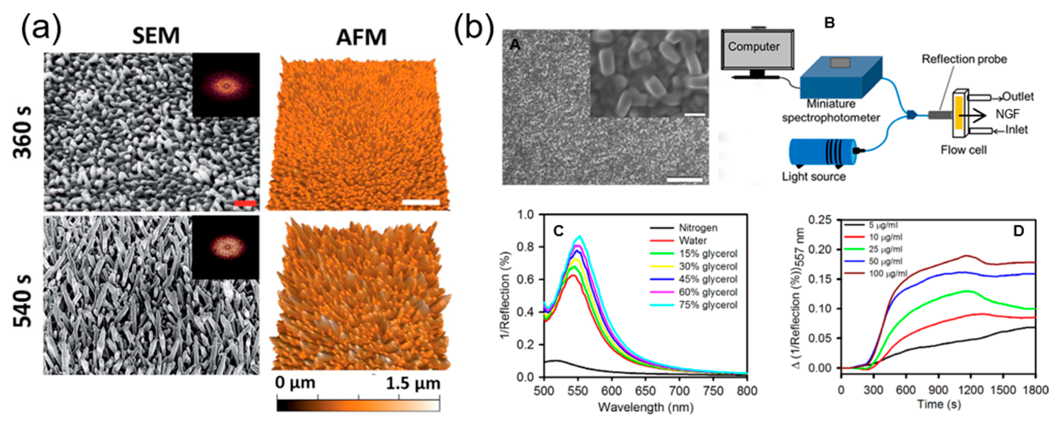
It is well known that random nanostructures have better LSPR sensitivity and SERS enhancement compared to their ordered counterparts. Electrochemical methods can create randomly oriented PANTFs on a conductive substrate without the use of a template. A review of electrochemical methods for preparing thin nanoporous gold films has been covered in an article previously [79]. The PANTFs can be prepared by either by adding different structure-directing agent or varying the deposition parameters. SEM images in Figure 7a,b show two completely different morphology of Au nanostructures prepared as a film with or without adding structure-directing agent. Figure 7a shows SEM and AFM images of a gold nanospike thin film prepared by providing a constant potential of 0.05 V versus Ag/AgCl (3M KCl) at different deposition times from HAuCl4 solution containing Pb (CH3COO)2 as a structure directing agent [80]. With the increase in deposition time from 360 s to 540 s, spike height increases drastically to 302 ± 57 nm. The shapes and size of nanostructures can also be tuned by changing the concentration of structure-directing agent. Figure 7b(A) is an SEM image of nanostructured gold film (NGF) prepared by providing −1.2 V for 60 s followed by −1.6 V for 30 s from 50 mM potassium dicyanoaurate solution [50]. Figure 7b(B) shows a typical reflection-based LSPR biosensing setup, where the fiber optic probe is used for both directing incident light for the excitation of surface plasmons and collecting the reflected light. The bulk refractive index sensitivity of the as-prepared NGF was determined by changing the environment of NGF with different concentrations of glycerol as shown in Figure 7b(C) and was found to be 100 ± 2 nm/RIU with FOM of 1.7. Figure 7b(D) shows real-time interactions of surface-immobilized carbohydrate mannose with different concentrations of lectin concanavalin A on NGF surface using reflection-based LSPR spectroscopy.
7.3. Transferred Films
The plasmonic-active individual nanoparticles and unsupported plasmonic-active thin films can be directly transferred to the solid supports creating PANTFs. Lang et al. prepared 100 nm thin film of nanoporous gold (np-Au) by chemically dealloying gold alloy film in 70% HNO3 [69]. The size of the pores of np-Au was controlled by varying the dealloying time from 5 min to 24 to create 10 to 50 nm. As-prepared np-Au thin film was transferred to glass slides to obtain the PANTFs with bulk refractive index sensitivity of nearly 210 nm/RIU and 264 nm/RIU for 30 and 50 nm pores, respectively.
8. Conclusions
The PANTFs have garnered huge attention in the field of plasmonics because of their ability to couple light with surface plasmons causing simultaneous excitation of SPP and LSPR. This can have a huge implication for improving and miniaturization of plasmonic and photonics-based devices as well as integrating them with microfluidics, quartz crystal microbalance, and electrochemical devices. In this review, we discussed propagating and localized surface plasmon resonance and recent advances in the synthetic methodologies for PANTFs. We also reviewed the advantages of using PANTFs compared to discrete nanostructures along with the comparison of the sensitivity of different types of PANTFs.
The discovery of PANTFs has led to the integration of plasmonics with quartz crystal microbalance, microfluidics, and electrochemistry. However, more work is needed in the field for improving sensitivity and simplifying the system for commercial use. As the research on plasmonics is expanding quickly, we can expect to see the integration of all the four fields in a single system in the near future.
Author Contributions
J.K.B.—conceptualization and original draft preparation; M.H.U.M.—review and additional writing; K.J.S.—Review, additional writing, editing, and funding acquisition. All authors have read and agreed to the published version of the manuscript.
Funding
The authors acknowledge the recent support of the work in this area by the University of Missouri–St. Louis and by the NIGMS awards R01-GM111835.
Conflicts of Interest
The authors declare no conflict of interest.
References
- Jauffred, L.; Samadi, A.; Klingberg, H.; Bendix, P.M.; Oddershede, L.B. Plasmonic heating of nanostructures. Chem. Rev. 2019, 119, 8087–8130. [Google Scholar] [CrossRef] [PubMed]
- Tokel, O.; Inci, F.; Demirci, U. Advances in plasmonic technologies for point of care applications. Chem. Rev. 2014, 114, 5728–5752. [Google Scholar] [CrossRef] [PubMed] [Green Version]
- Zeng, S.; Baillargeat, D.; Ho, H.-P.; Yong, K.-T. Nanomaterials enhanced surface plasmon resonance for biological and chemical sensing applications. Chem. Soc. Rev. 2014, 43, 3426–3452. [Google Scholar] [CrossRef]
- Willets, K.A.; Van Duyne, R.P. Localized surface plasmon resonance spectroscopy and sensing. Annu. Rev. Phys. Chem. 2007, 58, 267–297. [Google Scholar] [CrossRef] [Green Version]
- Homola, J. Surface plasmon resonance sensors for detection of chemical and biological species. Chem. Rev. 2008, 108, 462–493. [Google Scholar] [CrossRef]
- Mayer, K.M.; Hafner, J.H. Localized surface plasmon resonance sensors. Chem. Rev. 2011, 111, 3828–3857. [Google Scholar] [CrossRef]
- Jiang, N.; Zhuo, X.; Wang, J. Active plasmonics: Principles, structures, and applications. Chem. Rev. 2017, 118, 3054–3099. [Google Scholar] [CrossRef]
- Kang, H.; Buchman, J.T.; Rodriguez, R.S.; Ring, H.L.; He, J.; Bantz, K.C.; Haynes, C.L. Stabilization of silver and gold nanoparticles: Preservation and improvement of plasmonic functionalities. Chem. Rev. 2018, 119, 664–699. [Google Scholar] [CrossRef]
- Shao, L.; Susha, A.S.; Cheung, L.S.; Sau, T.K.; Rogach, A.L.; Wang, J. Plasmonic properties of single multispiked gold nanostars: Correlating modeling with experiments. Langmuir 2012, 28, 8979–8984. [Google Scholar] [CrossRef] [PubMed]
- Barbosa, S.; Agrawal, A.; Rodriguez-Lorenzo, L.; Pastoriza-Santos, I.; Alvarez-Puebla, R.A.; Kornowski, A.; Weller, H.; Liz-Marzan, L.M. Tuning size and sensing properties in colloidal gold nanostars. Langmuir 2010, 26, 14943–14950. [Google Scholar] [CrossRef] [PubMed]
- Couture, M.; Live, L.S.; Dhawan, A.; Masson, J.F. EOT or Kretschmann configuration? Comparative study of the plasmonic modes in gold nanohole arrays. Analyst 2012, 137, 4162–4170. [Google Scholar] [CrossRef] [PubMed]
- Rindzevicius, T.; Alaverdyan, Y.; Kaell, M.; Murray, W.A.; Barnes, W.L. Long-range refractive index sensing using plasmonic nanostructures. J. Phys. Chem. C 2007, 111, 11806–11810. [Google Scholar] [CrossRef]
- Bryche, J.F.; Gillibert, R.; Barbillon, G.; Gogol, P.; Moreau, J.; de la Chapelle, M.L.; Bartenlian, B.; Canva, M. Plasmonic enhancement by a continuous gold underlayer: Application to SERS sensing. Plasmonics 2016, 11, 601–608. [Google Scholar] [CrossRef]
- Henzie, J.; Lee, J.; Lee, M.H.; Hasan, W.; Odom, T.W. Nanofabrication of plasmonic structures. Annu. Rev. Phys. Chem. 2009, 60, 147–165. [Google Scholar] [CrossRef] [PubMed] [Green Version]
- Willets, K.A.; Wilson, A.J.; Sundaresan, V.; Joshi, P.B. Super-resolution imaging and plasmonics. Chem. Rev. 2017, 117, 7538–7582. [Google Scholar] [CrossRef] [PubMed]
- Susman, M.D.; Feldman, Y.; Vaskevich, A.; Rubinstein, I. Chemical deposition and stabilization of plasmonic copper nanoparticle films on transparent substrates. Chem. Mater. 2012, 24, 2501–2508. [Google Scholar] [CrossRef]
- Li, W.; Ren, K.; Zhou, J. Aluminum-based localized surface plasmon resonance for biosensing. Trends Anal. Chem. 2016, 80, 486–494. [Google Scholar] [CrossRef]
- Huang, X.; Tang, S.; Mu, X.; Dai, Y.; Chen, G.; Zhou, Z.; Ruan, F.; Yang, Z.; Zheng, N. Freestanding palladium nanosheets with plasmonic and catalytic properties. Nat. Nanotech. 2011, 6, 28–32. [Google Scholar] [CrossRef]
- Reddy, H.; Guler, U.; Kudyshev, Z.; Kildishev, A.V.; Shalaev, V.M.; Boltasseva, A. Temperature-dependent optical properties of plasmonic titanium nitride thin films. ACS Photonics 2017, 4, 1413–1420. [Google Scholar] [CrossRef]
- Gopalan, K.K.; Paulillo, B.; Mackenzie, D.M.; Rodrigo, D.; Bareza, N.; Whelan, P.R.; Shivayogimath, A.; Pruneri, V. Scalable and tunable periodic graphene nanohole arrays for mid-infrared plasmonics. Nano Lett. 2018, 18, 5913–5918. [Google Scholar] [CrossRef]
- Agrawal, A.; Cho, S.H.; Zandi, O.; Ghosh, S.; Johns, R.W.; Milliron, D.J. Localized surface plasmon resonance in semiconductor nanocrystals. Chem. Rev. 2018, 118, 3121–3207. [Google Scholar] [CrossRef] [PubMed]
- Wu, Y.; Niu, J.; Danesh, M.; Liu, J.; Chen, Y.; Ke, L.; Qiu, C.; Yang, H. Localized surface plasmon resonance in graphene nanomesh with Au nanostructures. Appl. Phys. Lett. 2016, 109, 041106. [Google Scholar] [CrossRef] [Green Version]
- Dong, P.; Lin, Y.; Deng, J.; Di, J. Ultrathin gold-shell coated silver nanoparticles onto a glass platform for improvement of plasmonic sensors. ACS Appl. Mater. Interfaces 2013, 5, 2392–2399. [Google Scholar] [CrossRef] [PubMed]
- Abargues, R.; Nickel, U.; Rodriguez-Canto, P. Charge dissipation in e-beam lithography with Novolak-based conducting polymer films. Nanotechnology 2008, 19, 125302. [Google Scholar] [CrossRef]
- Shir, D.; Ballard, Z.S.; Ozcan, A. Flexible plasmonic sensors. IEEE J. Sel. Top. Quantum Electron. 2015, 22, 12–20. [Google Scholar] [CrossRef] [Green Version]
- Sugavaneshwar, R.P.; Ishii, S.; Dao, T.D.; Ohi, A.; Nabatame, T.; Nagao, T. Fabrication of highly metallic TiN films by pulsed laser deposition method for plasmonic applications. ACS Photonics 2017, 5, 814–819. [Google Scholar] [CrossRef]
- Lin, E.H.; Tsai, W.S.; Lee, K.L.; Lee, M.C.M.; Wei, P.K. Enhancing angular sensitivity of plasmonic nanostructures using mode transition in hexagonal gold nanohole arrays. Sens. Actuators B Chem. 2017, 241, 800–805. [Google Scholar] [CrossRef]
- Chuo, Y.; Hohertz, D.; Landrock, C.; Omrane, B.; Kavanagh, K.L.; Kaminska, B. Large-area low-cost flexible plastic nanohole arrays for integrated bio-chemical sensing. IEEE Sens. J. 2013, 13, 3982–3990. [Google Scholar] [CrossRef]
- Aouani, H.; Wenger, J.; Gérard, D.; Rigneault, H.; Devaux, E.; Ebbesen, T.W.; Mahdavi, F.; Xu, T.; Blair, S. Crucial role of the adhesion layer on the plasmonic fluorescence enhancement. ACS Nano 2009, 3, 2043–2048. [Google Scholar] [CrossRef]
- Habteyes, T.G.; Dhuey, S.; Wood, E.; Gargas, D.; Cabrini, S.; Schuck, P.J.; Alivisatos, A.P.; Leone, S.R. Metallic adhesion layer induced plasmon damping and molecular linker as a nondamping alternative. ACS Nano 2012, 6, 5702–5709. [Google Scholar] [CrossRef]
- Zhu, S.; Du, C.; Fu, Y.; Deng, Q.; Shi, L. Influence of Cr adhesion layer on detection of amyloid-derived diffusible ligands based on localized surface plasmon resonance. Plasmonics 2009, 4, 135–140. [Google Scholar] [CrossRef] [Green Version]
- Najiminaini, M.; Vasefi, F.; Kaminska, B.; Carson, J. Optical resonance transmission properties of nano-hole arrays in a gold film: Effect of adhesion layer. Opt. Express 2011, 19, 26186–26197. [Google Scholar] [CrossRef] [PubMed]
- Todeschini, M.; Bastos Da Silva Fanta, A.; Jensen, F.; Wagner, J.B.; Han, A. Influence of Ti and Cr adhesion layers on ultrathin Au films. ACS Appl. Mater. Interfaces 2017, 9, 37374–37385. [Google Scholar] [CrossRef] [PubMed] [Green Version]
- Siegfried, T.; Ekinci, Y.; Martin, O.J.; Sigg, H. Engineering metal adhesion layers that do not deteriorate plasmon resonances. ACS Nano 2013, 7, 2751–2757. [Google Scholar] [CrossRef] [Green Version]
- Cortie, M.B.; McDonagh, A.M. Synthesis and optical properties of hybrid and alloy plasmonic nanoparticles. Chem. Rev. 2011, 111, 3713–3735. [Google Scholar] [CrossRef] [Green Version]
- Baburin, A.S.; Merzlikin, A.M.; Baryshev, A.V.; Ryzhikov, I.A.; Panfilov, Y.V.; Rodionov, I.A. Silver-based plasmonics: Golden material platform and application challenges. Opt. Mater. Express 2019, 9, 611–642. [Google Scholar] [CrossRef]
- Horák, M.; Bukvišová, K.; Švarc, V.; Jaskowiec, J.; Křápek, V.; Šikola, T. Comparative study of plasmonic antennas fabricated by electron beam and focused ion beam lithography. Sci. Rep. 2018, 8, 9640. [Google Scholar] [CrossRef]
- Arnob, M.M.P.; Zhao, F.; Li, J.; Shih, W.C. EBL-based fabrication and different modeling approaches for nanoporous gold nanodisks. ACS Photonics 2017, 4, 1870–1878. [Google Scholar] [CrossRef]
- Vieu, C.; Carcenac, F.; Pepin, A.; Chen, Y.; Mejias, M.; Lebib, A.; Manin-Ferlazzo, L.; Couraud, L.; Launois, H. Electron beam lithography: Resolution limits and applications. Appl. Surf. Sci. 2000, 164, 111–117. [Google Scholar] [CrossRef]
- Haynes, C.L.; Van Duyne, R.P. Nanosphere lithography: A versatile nanofabrication tool for studies of size-dependent nanoparticle optics. J. Phys. Chem. B 2001, 105, 5599–5611. [Google Scholar] [CrossRef]
- Hicks, E.M.; Zhang, X.; Zou, S.; Lyandres, O.; Spears, K.G.; Schatz, G.C.; Van Duyne, R.P. Plasmonic properties of film over nanowell surfaces fabricated by nanosphere lithography. J. Phys. Chem. B 2005, 109, 22351–22358. [Google Scholar] [CrossRef] [PubMed]
- Halpern, A.R.; Corn, R.M. Lithographically patterned electrodeposition of gold, silver, and nickel nanoring arrays with widely tunable near-infrared plasmonic resonances. ACS Nano 2013, 7, 1755–1762. [Google Scholar] [CrossRef]
- Prikulis, J.; Hanarp, P.; Olofsson, L.; Sutherland, D.; Kaell, M. Optical spectroscopy of nanometric holes in thin gold films. Nano Lett. 2004, 4, 1003–1007. [Google Scholar] [CrossRef]
- Im, H.; Lee, S.H.; Wittenberg, N.J.; Johnson, T.W.; Lindquist, N.C.; Nagpal, P.; Norris, D.J.; Oh, S.H. Template-stripped smooth Ag nanohole arrays with silica shells for surface plasmon resonance biosensing. ACS Nano 2011, 5, 6244–6253. [Google Scholar] [CrossRef] [PubMed] [Green Version]
- Es-Souni, M.; Habouti, S. Ordered nanomaterial thin films via supported anodized alumina templates. Front. Mater. 2014, 1, 19. [Google Scholar] [CrossRef] [Green Version]
- Yeom, S.H.; Kim, O.G.; Kang, B.H.; Kim, K.J.; Yuan, H.; Kwon, D.H.; Kim, H.R.; Kang, S.W. Highly sensitive nano-porous lattice biosensor based on localized surface plasmon resonance and interference. Opt. Express 2011, 19, 22882–22891. [Google Scholar] [CrossRef]
- McPhillips, J.; Murphy, A.; Jonsson, M.P.; Hendren, W.R.; Atkinson, R.; Höök, F.; Zayats, A.V.; Pollard, R.J. High-performance biosensing using arrays of plasmonic nanotubes. ACS Nano 2010, 4, 2210–2216. [Google Scholar] [CrossRef]
- Kabashin, A.; Evans, P.; Pastkovsky, S.; Hendren, W.; Wurtz, G.; Atkinson, R.; Pollard, R.; Podolskiy, V.; Zayats, A. Plasmonic nanorod metamaterials for biosensing. Nat. Mater. 2009, 8, 867. [Google Scholar] [CrossRef]
- Hahn, C.; Hajebifard, A.; Berini, P. Helium focused ion beam direct milling of plasmonic heptamer-arranged nanohole arrays. Nanophotonics 2019. [Google Scholar] [CrossRef]
- Bhattarai, J.K.; Sharma, A.; Fujikawa, K.; Demchenko, A.V.; Stine, K.J. Electrochemical synthesis of nanostructured gold film for the study of carbohydrate-lectin interactions using localized surface plasmon resonance spectroscopy. Carbohydr. Res. 2015, 405, 55–65. [Google Scholar] [CrossRef] [Green Version]
- Stiles, P.L.; Dieringer, J.A.; Shah, N.C.; Van Duyne, R.P. Surface-enhanced Raman spectroscopy. Annu. Rev. Anal. Chem. 2008, 1, 601–626. [Google Scholar] [CrossRef] [PubMed] [Green Version]
- Canalejas-Tejero, V.; Herranz, S.; Bellingham, A.; Moreno-Bondi, M.C.; Barrios, C.A. Passivated aluminum nanohole arrays for label-free biosensing applications. ACS Appl. Mater. Interfaces 2014, 6, 1005–1010. [Google Scholar] [CrossRef] [PubMed]
- Lee, S.H.; Johnson, T.W.; Lindquist, N.C.; Im, H.; Norris, D.J.; Oh, S.H. Linewidth-optimized extraordinary optical transmission in water with template-stripped metallic nanohole arrays. Adv. Funct. Mater. 2012, 22, 4439–4446. [Google Scholar] [CrossRef]
- Zhang, X.; Li, Z.; Ye, S.; Wu, S.; Zhang, J.; Cui, L.; Li, A.; Wang, T.; Li, S.; Yang, B. Elevated Ag nanohole arrays for high performance plasmonic sensors based on extraordinary optical transmission. J. Mater. Chem. 2012, 22, 8903–8910. [Google Scholar] [CrossRef]
- Brolo, A.G.; Gordon, R.; Leathem, B.; Kavanagh, K.L. Surface plasmon sensor based on the enhanced light transmission through arrays of nanoholes in gold films. Langmuir 2004, 20, 4813–4815. [Google Scholar] [CrossRef]
- Lee, S.H.; Bantz, K.C.; Lindquist, N.C.; Oh, S.H.; Haynes, C.L. Self-assembled plasmonic nanohole arrays. Langmuir 2009, 25, 13685–13693. [Google Scholar] [CrossRef]
- Rindzevicius, T.; Alaverdyan, Y.; Dahlin, A.; Hoeoek, F.; Sutherland, D.S.; Kaell, M. Plasmonic sensing characteristics of single nanometric holes. Nano Lett. 2005, 5, 2335–2339. [Google Scholar] [CrossRef]
- Chen, J.; Shi, J.; Decanini, D.; Cambril, E.; Chen, Y.; Haghiri-Gosnet, A.M. Gold nanohole arrays for biochemical sensing fabricated by soft UV nanoimprint lithography. Microelectron. Eng. 2009, 86, 632–635. [Google Scholar] [CrossRef]
- Live, L.S.; Bolduc, O.R.; Masson, J.F. Propagating surface plasmon resonance on microhole arrays. Anal. Chem. 2010, 82, 3780–3787. [Google Scholar] [CrossRef]
- Ai, B.; Yu, Y.; Möhwald, H.; Zhang, G. Novel 3D Au nanohole arrays with outstanding optical properties. Nanotechnology 2012, 24, 035303. [Google Scholar] [CrossRef]
- Luo, X.; Xing, Y.; Galvan, D.D.; Zheng, E.; Wu, P.; Cai, C.; Yu, Q. A plasmonic gold nanohole array for surface-enhanced Raman scattering detection of DNA methylation. ACS Sens. 2019. [Google Scholar] [CrossRef] [PubMed]
- Xiang, G.; Zhang, N.; Zhou, X. Localized surface plasmon resonance biosensing with large area of gold nanoholes fabricated by nanosphere lithography. Nanoscale Res. Lett. 2010, 5, 818–822. [Google Scholar] [CrossRef] [PubMed] [Green Version]
- Saito, M.; Kitamura, A.; Murahashi, M.; Yamanaka, K.; Hoa, L.Q.; Yamaguchi, Y.; Tamiya, E. Novel gold-capped nanopillars imprinted on a polymer film for highly sensitive plasmonic biosensing. Anal. Chem. 2012, 84, 5494–5500. [Google Scholar] [CrossRef] [PubMed]
- Zheng, J.; Yang, W.; Wang, J.; Zhu, J.; Qian, L.; Yang, Z. An ultranarrow SPR linewidth in the UV region for plasmonic sensing. Nanoscale 2019, 11, 4061–4066. [Google Scholar] [CrossRef]
- Norek, M.; Włodarski, M.; Matysik, P. UV plasmonic-based sensing properties of aluminum nanoconcave arrays. Curr. Appl. Phys. 2014, 14, 1514–1520. [Google Scholar] [CrossRef]
- Sharma, B.; Cardinal, M.F.; Ross, M.B.; Zrimsek, A.B.; Bykov, S.V.; Punihaole, D.; Asher, S.A.; Schatz, G.C.; Van Duyne, R.P. Aluminum film-over-nanosphere substrates for deep-UV surface-enhanced resonance Raman spectroscopy. Nano Lett. 2016, 16, 7968–7973. [Google Scholar] [CrossRef]
- Kim, D.K.; Yoo, S.M.; Park, T.J.; Yoshikawa, H.; Tamiya, E.; Park, J.Y.; Lee, S.Y. Plasmonic properties of the multispot copper-capped nanoparticle array chip and its application to optical biosensors for pathogen detection of multiplex DNAs. Anal. Chem. 2011, 83, 6215–6222. [Google Scholar] [CrossRef]
- Liu, B.; Chen, S.; Zhang, J.; Yao, X.; Zhong, J.; Lin, H.; Huang, T.; Yang, Z.; Zhu, J.; Liu, S. A plasmonic sensor array with ultrahigh figures of merit and resonance linewidths down to 3 nm. Adv. Mater. 2018, 30, 1706031. [Google Scholar] [CrossRef]
- Lang, X.; Qian, L.; Guan, P.; Zi, J.; Chen, M. Localized surface plasmon resonance of nanoporous gold. Appl. Phys. Lett. 2011, 98, 093701. [Google Scholar] [CrossRef]
- Ebbesen, T.W.; Lezec, H.J.; Ghaemi, H.; Thio, T.; Wolff, P.A. Extraordinary optical transmission through sub-wavelength hole arrays. Nature 1998, 391, 667. [Google Scholar] [CrossRef]
- Park, T.H.; Mirin, N.; Lassiter, J.B.; Nehl, C.L.; Halas, N.J.; Nordlander, P. Optical properties of a nanosized hole in a thin metallic film. ACS Nano 2008, 2, 25–32. [Google Scholar] [CrossRef]
- Jonsson, M.P.; Dahlin, A.B.; Feuz, L.; Petronis, S.; Hoeoek, F. Locally functionalized short-range ordered nanoplasmonic pores for bioanalytical sensing. Anal. Chem. 2010, 82, 2087–2094. [Google Scholar] [CrossRef]
- Nagpal, P.; Lindquist, N.C.; Oh, S.H.; Norris, D.J. Ultrasmooth patterned metals for plasmonics and metamaterials. Science 2009, 325, 594–597. [Google Scholar] [CrossRef] [PubMed]
- Cushing, S.K.; Hornak, L.A.; Lankford, J.; Liu, Y.; Wu, N. Origin of localized surface plasmon resonances in thin silver film over nanosphere patterns. Appl. Phys. A 2011, 103, 955–958. [Google Scholar] [CrossRef]
- Zhang, X.; Young, M.A.; Lyandres, O.; Van Duyne, R.P. Rapid detection of an anthrax biomarker by surface-enhanced Raman spectroscopy. J. Am. Chem. Soc. 2005, 127, 4484–4489. [Google Scholar] [CrossRef] [PubMed]
- Zhang, X.; Zhao, J.; Whitney, A.V.; Elam, J.W.; Van Duyne, R.P. Ultrastable substrates for surface-enhanced Raman spectroscopy: Al2O3 overlayers fabricated by atomic layer deposition yield improved anthrax biomarker detection. J. Am. Chem. Soc. 2006, 128, 10304–10309. [Google Scholar] [CrossRef] [PubMed]
- Masson, J.F.; Gibson, K.F.; Provencher-Girard, A. Surface-enhanced Raman spectroscopy amplification with film over etched nanospheres. J. Phys. Chem. C 2010, 114, 22406–22412. [Google Scholar] [CrossRef]
- Lee, J.; Zhang, Q.; Park, S.; Choe, A.; Fan, Z.; Ko, H. Particle-film plasmons on periodic silver film over nanosphere (AgFON): A hybrid plasmonic nanoarchitecture for surface-enhanced Raman spectroscopy. ACS Appl. Mater. Interfaces 2016, 8, 634–642. [Google Scholar] [CrossRef]
- Bhattarai, J.K.; Neupane, D.; Nepal, B.; Mikhaylov, V.; Demchenko, A.V.; Stine, K.J. Preparation, modification, characterization, and biosensing application of nanoporous gold using electrochemical techniques. Nanomaterials 2018, 8, 171. [Google Scholar] [CrossRef] [Green Version]
- Elbourne, A.; Coyle, V.E.; Truong, V.K.; Sabri, Y.M.; Kandjani, A.E.; Bhargava, S.K.; Ivanova, E.P.; Crawford, R.J. Multi-directional electrodeposited gold nanospikes for antibacterial surface applications. Nanoscale Adv. 2019, 1, 203–212. [Google Scholar] [CrossRef] [Green Version]
Figure 1.
Schematic diagrams illustrating the excitation of surface plasmons from (a) thin film using prism as a coupling device, generating propagating surface plasmon or surface plasmon polariton (SPP), and (b) nanoparticle, generating a localized surface plasmon resonance (LSPR). The typical spectra that can be obtained after the surface plasmon excitation are shown on the right.

Figure 2.
Schematic of commonly applied strategies for the synthesis of plasmonic-active nanostructured thin films starting from (a) deposition on patterned template, (b) deposition on patterned substrate, (c) deposition on planar substrate, and (d) transfer on planar substrate.
Figure 2.
Schematic of commonly applied strategies for the synthesis of plasmonic-active nanostructured thin films starting from (a) deposition on patterned template, (b) deposition on patterned substrate, (c) deposition on planar substrate, and (d) transfer on planar substrate.

Figure 3.
(a) Schematic representation of process steps for fabricating nanohole arrays using nanosphere lithography. (b) SEM images of (top) the resulting large area (~30 × 30 µm2) single crystalline hexagonal nanohole array, (middle) an elliptical nanohole array (60° tilt angle) after nanosphere removal, and (bottom) after 4 min Ag electroless plating onto the nanohole array. (c) SERS spectra of (A) 4 min Ag plated nanohole array, (B) 4 min Ag plated flat silver film, (C) a standard nanohole array, and (D) 5× a flat silver film. All substrates were exposed to 1 mM benzenethiol prior to SERS measurements. P = 0.32 mW, t = 180 s, and λmax = 532 nm. Reproduced (a,c) and adapted (b) with permission from Reference [56], Copyright 2009, American Chemical Society.
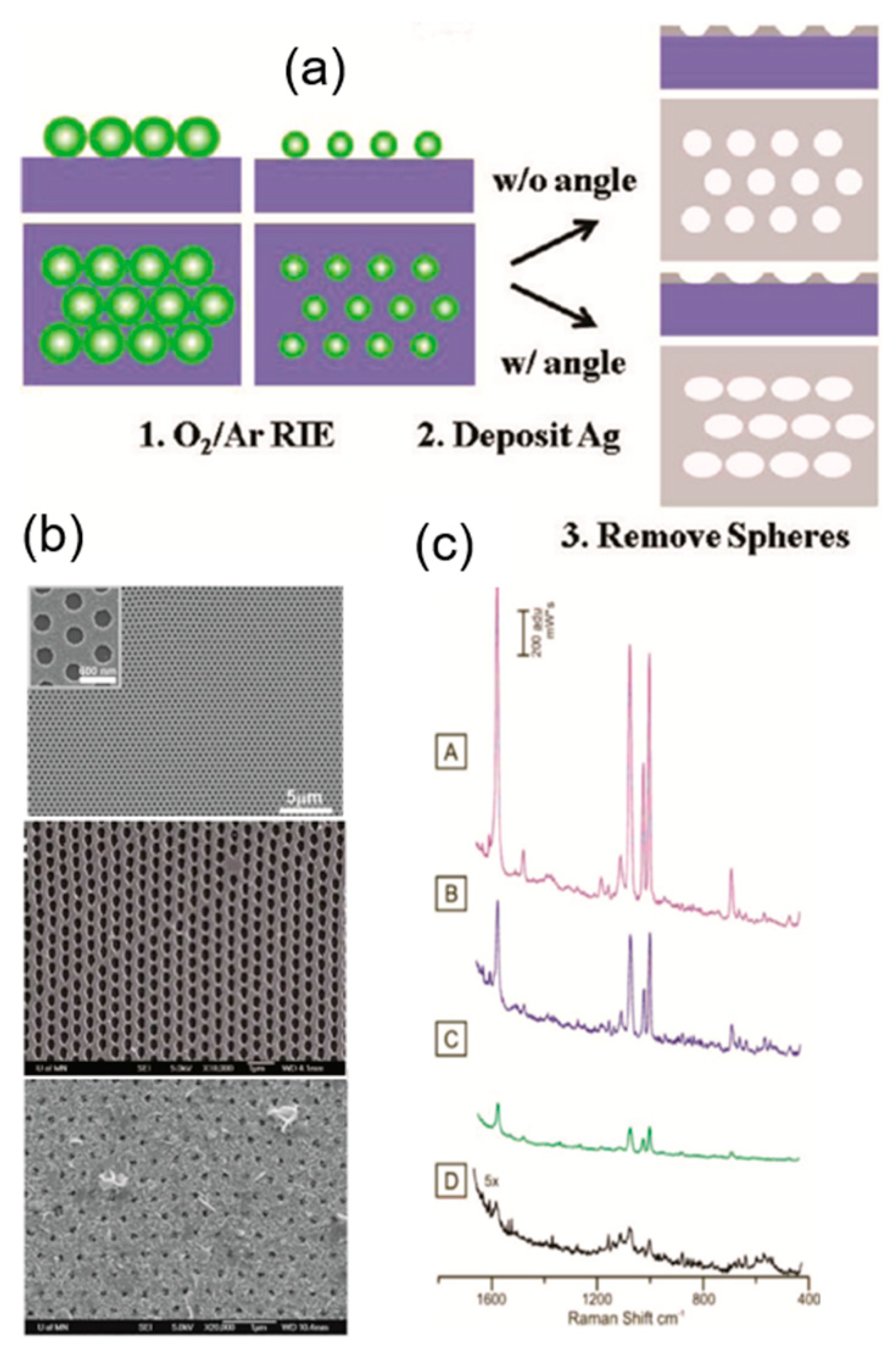
Figure 4.
(A) Schematic for fabricating the large-area nanohole arrays. (a) A thermal resist layer spun on a Si wafer is imprinted with a nanoimprint stamp with circular post patterns. (b) The Si wafer is subsequently etched to be a nanohole template with deep circular trenches. (c) A metal film is directionally deposited on the Si template. (d) The metal surface is coated with a thin layer of epoxy and covered with a glass slide. The Ag film is then peeled off of the template to reveal the smooth nanohole array made in the metal film. The Si template can be reused to make multiple identical samples. (B) (a) A SEM image of the Si template with deep circular trenches. (b) A cross-sectional SEM image of the Si template after depositing a 100 nm thick Ag film. (c) A SEM image of the template-stripped Ag periodic nanohole array. The inset shows a zoomed-in image of the template-stripped Ag nanoholes. The diameter of the nanoholes and periodicity of the array are 180 and 500 nm, respectively. (d) A photograph of the fabricated nanohole array chip. A 26.5 mm × 26.5 mm area of 100 nm-thick Ag film with nanohole patterns in an 8 mm × 8 mm area in the center is transferred to a standard microscope slide. The inset in panel d shows a photograph of a multi-channel PDMS chip attached on the silica-coated nanohole array chip. Reproduced with permission from Reference [44], Copyright 2011, American Chemical Society.
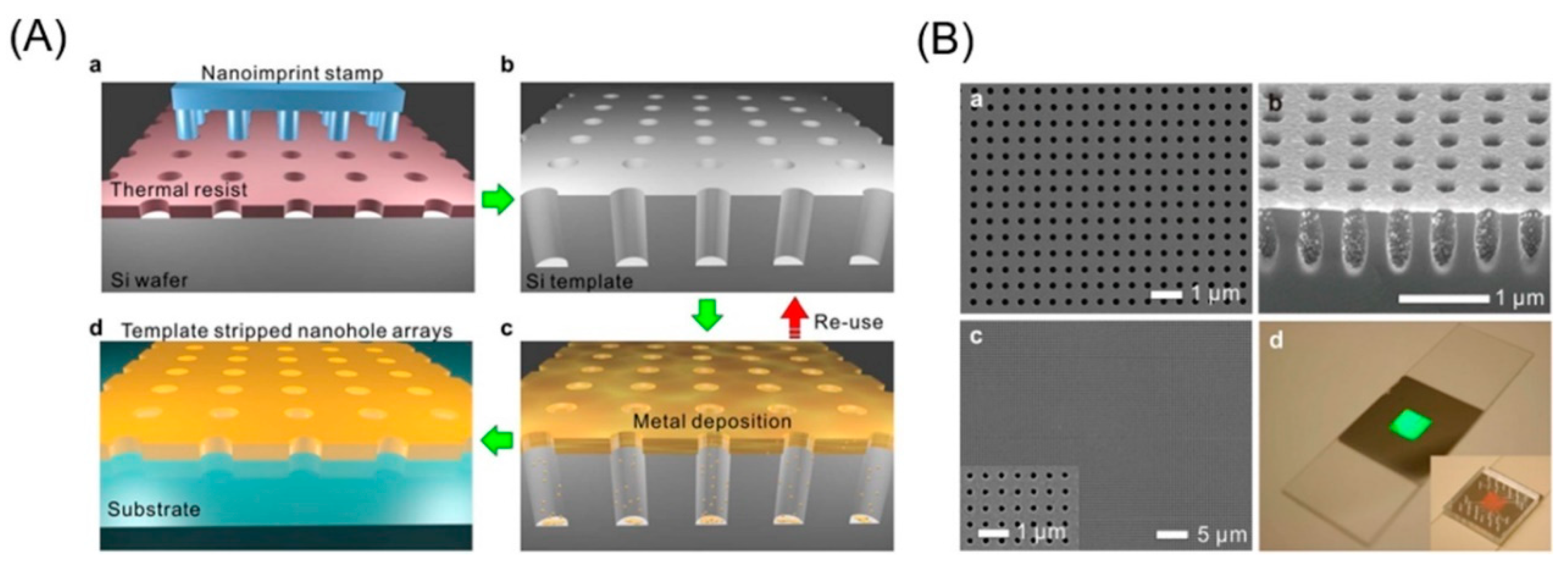
Figure 5.
SEM images of AgFON-505 (a), AuNP-AgFON-505 (b), with cross-sectional image of AuNP-AgFON-505 (c). Raman spectra of AuNP-AgFON-505, AgFON-505, and AuNP-Ag film substrates (d). Raman mapping images of AuNP-AgFON-505 versus AgFON-505 at 785 nm excitation laser (e,f). (g) FDTD simulations of E-fields on AuNP assemblies on AgFON-505 substrate at 785 nm laser wavelength. Partially enlarged image for dimer AuNPs (g1) and crevice gap (g2) in AuNP-AgFON-505 system. Reproduced with permission from Reference [78], Copyright 2016, American Chemical Society.

Figure 6.
(a) Schematic illustration of preparation of the film over nanowell surfaces. (b) SEM images of Ag film over nanowell surface [diameter of nanospheres (D) = 510 nm; mass thickness of Ag film (dm) = 50 nm; and etch time (te) = 10 min]. (A) Well-packed area of over 40 µm2 and (B) magnified image of the same sample. The SEM accelerating voltage was 5 kV. (c) (A) Collection of reflectance spectra of Ag film over nanowell surface in different solvents (D = 590 nm; dm = 50 nm). (B) Plots of λmin (solvent)–λmin (dry nitrogen) versus refractive index of the solvent for three nanosphere sizes: D = 450, 510, and 590 nm. Each data point represents the average value obtained from at least three surfaces. Error bars show the standard deviations. For all surface preparations, dm = 50 nm and te = 10 min. Reproduced with permission from Reference [41], Copyright 2005, American Chemical Society.
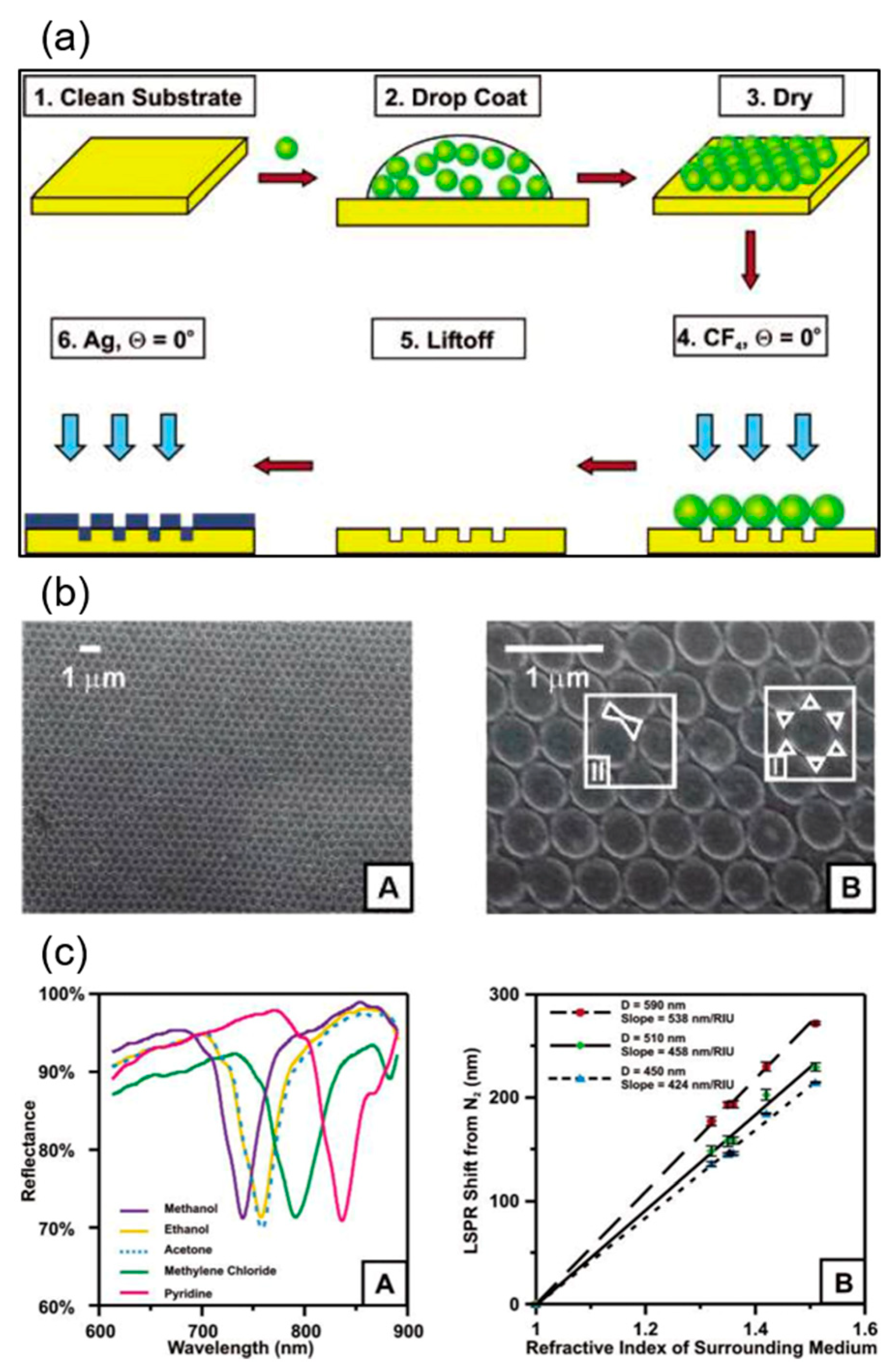
Figure 7.
(a) Native surface data for the nanospike deposition from precursor solution of 6.8 mM HAuCl4 and 1 mM Pb(CH3COO)2: column (1) SEM (45° tilted) and column (2) AFM images of the gold nanospike surfaces as a function of electrodeposition time. The red and white scale bars are 200 nm and 1 mm, respectively. 2D-FFT data (insets) are shown for the top-down SEM images. Adapted with permission from Reference [80], Copyright 2018, The Royal Society of Chemistry. (b) (A) SEM images of nanostructured gold film (NGF) prepared by providing −1.2 V for 60 s followed by −1.6 V for 30 s (vs. Ag/AgCl (KCl, Satd) from 50 mM potassium dicyanoaurate. Scale bars: 2 µm. Insets are the corresponding higher magnification SEM images (scale bars: 0.2 µm). (B) Optical set up for localized surface plasmon resonance spectroscopy in reflection mode. (C) Bulk refractive index response of as-prepared NGF evident by change in LSPR peak wavelength. (D) Real-time LSPR response of self-assembled monolayer (SAM)-modified NGF to different concentrations of Concanavalin A. NGF was surface modified with a mixed SAM of αMan-C8-SH and TEG-SH (1:3). Reproduced with permission from Reference [50], Copyright 2014, Elsevier Ltd.

Table 1.
Sensitivity of plasmonic-active nanostructured thin films.
| NS | M | Fabrication Method | d/p/t (nm) | λmax (nm) Air or N2 | Method | Sensitivity R = (nm/RIU), FOM, E | Ref |
|---|---|---|---|---|---|---|---|
| NH | Al | EBE/EBL/Etching | 220/-/100 | 510 | LSPR | R = 487 | [52] |
| Ag | NH Si template/EBE/peel off | 180/500/100 | NA | LSPR | R = 450 | [44] | |
| NH Si template/EBE/peel off | 100/500/200 | NA | LSPR | R = 494 | [53] | ||
| NSL/RIE/deposition | 290/-/80 | 550/790 | LSPR | R = 252 | [54] | ||
| NSL/RIE/deposition/HF etching | 290/-/80 | 655 | LSPR | R = 648 | |||
| deposition/FIB | 200/545/100 | 645 | LSPR | R = 400 | [55] | ||
| NSL/RIE/EBE/lift-off | ~300/400/50 | 672 | SERS | E = 8.13 × 10⁵ | [56] | ||
| NSL/RIE/EBE/lift-off/plating | <300/400/>50 | NA | SERS | E = 3 × 10⁶ | |||
| Au | NSL/RIE/EBE/lift-off | 60/-/20 | ~620 | LSPR | R = ~70 | [57] | |
| NSL/RIE/EBE/lift-off | 60/-/20 | 675 ± 10 | LSPR (1 hole) | R = ~90 | |||
| NSL/PVD/lift-off | 60/-/20 | 575 | LSPR | R = ~100 | [43] | ||
| UV-NL/RIE/EBE/lift-off | 200/400/50 | 583 | LSPR | R = 150 | [58] | ||
| NSL/RIE/EBE/lift-off | 70/ | NA | SPP | R = >3000 | [59] | ||
| NSL/RIE/EBE/lift-off | 500/-/80 | 1489 | LSPR | R = 375 | [60] | ||
| NSL/EBE/mask/RIE/mask removal/lift-off | 500/-/80 | 898 | LSPR | R = 625 | |||
| NSL/RIE/sputtering/lift-off | 600/1000/125 | 710 | LSPR | R = 530 ± 30 FOM = 132 | [11] | ||
| 600/1000/125 | NA | SPP | R = 3600 ± 200 FOM = 327 | ||||
| EBL/PVD | 100/585/50 | NA | SERS | E = ~106 | [61] | ||
| NSL/PVD/lift-off | 125/-/40 | 575 | LSPR | R = 36 | [62] | ||
| NPi | Au | porous Al2O3 imprinted nanopillars of Cyclo-olefin polymer/sputter | 30.0–39.9/-/50 | NA | LSPR | R = 154 | [63] |
| Au thin film/Porous Al2O3/ED | Film t = 5 nm 25/60/380 | NA | SPP | R = 32,000 FOM = >330 | [48] | ||
| Al | LIL/deposition | 180/400/150 | 310 | SPP | R = 223 FOM = 8 | [64] | |
| 180/400/150 | 413 | SPP | R = 485 FOM = 20 | ||||
| NC | Al | EA (120 V)/removal Al2O3 | /246.3/ | 250 | LSPR | R = 191 | [65] |
| EA (195 V)/removal of Al2O3 | /456.7/ | 350 | LSPR | R = 291 | |||
| FON | Al | NSL/PVD | 210/-/200 | NA | SERS | E = ~104–105 | [66] |
| NPA | Cu | NSL/EBE | 100/-/30 | 580 | LSPR | R = 67.8 | [67] |
| HA | Au | THL/EBE | 620/620/100 | NA | SPP | FOM = 730 | [68] |
| NGF | Au | Au thin film/ED | 100–200/-/200 | 518 ± 1 | LSPR | R = 100 ± 2 | [50] |
| NPG | Au | Dealloyed unsupported thin film in HNO3/transferred to substrate | 30/-/100 | ~510 | LSPR | R = 210 | [69] |
| 50/-/100 | NA | LSPR | R = 264 |
Notes: NS = Nanostructures; NH = nanohole; NPi = nanopillar; NC = nanoconcave; FON = film over nanosphere; NPA = nanoparticle array; HA = hexagonal array; NGF = nanostructured gold film; NPG = nanoporous gold; RIS = bulk refractive index sensitivity; E = enhancement factor; EBE = electron beam evaporation; PVD = physical vapor deposition; EBL = electron beam lithography; LIL = laser interference lithography; THL = tunable holographic lithography; ED = Electrochemical deposition; NL = nanoimprint lithography; EA = electrochemical anodization; d = diameter of hole; p = periodicity and t = thickness of the film; FOM = figure of merit.
© 2020 by the authors. Licensee MDPI, Basel, Switzerland. This article is an open access article distributed under the terms and conditions of the Creative Commons Attribution (CC BY) license (http://creativecommons.org/licenses/by/4.0/).
Share and Cite
MDPI and ACS Style
Bhattarai, J.K.; Maruf, M.H.U.; Stine, K.J. Plasmonic-Active Nanostructured Thin Films. Processes 2020, 8, 115. https://doi.org/10.3390/pr8010115
AMA Style
Bhattarai JK, Maruf MHU, Stine KJ. Plasmonic-Active Nanostructured Thin Films. Processes. 2020; 8(1):115. https://doi.org/10.3390/pr8010115
Chicago/Turabian StyleBhattarai, Jay K., Md Helal Uddin Maruf, and Keith J. Stine. 2020. "Plasmonic-Active Nanostructured Thin Films" Processes 8, no. 1: 115. https://doi.org/10.3390/pr8010115
Note that from the first issue of 2016, this journal uses article numbers instead of page numbers. See further details here.