Two-Dimensional Dynamic Beam Steering by Tamm Plasmon Polariton


1
Kirensky Institute of Physics, Federal Research Center, Krasnoyarsk Science Center of the Siberian Branch of the Russian Academy of Sciences, 660036 Krasnoyarsk, Russia
2
Siberian Federal University, 660041 Krasnoyarsk, Russia
3
College of Photonics, National Yang Ming Chiao Tung University, Tainan 711, Taiwan
4
Institute of Photonics Technologies, National Tsing Hua University, Hsinchu 300, Taiwan
*
Author to whom correspondence should be addressed.
Photonics 2023, 10(10), 1151; https://doi.org/10.3390/photonics10101151
Submission received: 22 August 2023
/
Revised: 9 October 2023
/
Accepted: 10 October 2023
/
Published: 13 October 2023
Abstract
:The dynamic steering of a beam reflected from a photonic structure supporting Tamm plasmon polariton is demonstrated. The phase and amplitude of the reflected wave are adjusted by modulating the refractive index of a transparent conductive oxide layer by applying a bias voltage. It is shown that the proposed design allows for two-dimensional beam steering by deflecting the light beam along the polar and azimuthal angles.
1. Introduction
The control of light wave amplitude and phase is crucial for designing light detection and ranging devices (LIDAR). Significant advances in subwavelength technologies, such as photo- or electronic lithography, have made it possible to create solid-state LIDARs [1,2,3], in which the optical properties of light are controlled by metasurfaces—structures consisting of subwavelength elements. Metasurfaces open up new opportunities for implementation of holograms [4], lenses [5], media with anomalous reflection [6,7], lasers [8,9], perfect absorbers with critical coupling [10,11], sensors [12,13] etc. An actively tuned metasurface with control of the phase and amplitude of individual elements ensures the generation of an arbitrarily complex wave front. There are several approaches to actively rearrange optical properties of a photonic structure. The first one is infiltration of liquid crystals under the metasurface [14,15,16,17]. The advantage of this method is the control over optical properties via variation in both electric field and temperature. However, one of the key drawbacks of such devices is their switching time: as large as several milliseconds. Another promising approach is application of phase-change materials, such as vanadium dioxide [18,19] and GST [20]. In this case, switching occurs three orders of magnitude faster than in structures based on liquid crystals, but this switching is discrete. Particular attention should be paid to the investigation held by Prof. Atwater and Dr. Huang Y.-W.’s groups, in which the possibility of replacing conventional semiconductor materials with transparent conductive oxides was demonstrated [21,22]. It has been shown that the applied bias voltage decreases the real part of the dielectric permittivity of the conductive oxide. As a result, a significant phase jump near the gap plasmon resonant wavelength is provided. A similar effect was demonstrated in [23], where the gap plasmon resonance was replaced by the Tamm plasmon polariton (TPP). TPP is analogous to the Tamm surface states in condensed matter physics [24]. This state can be excited between a photonic crystal and a medium with negative permittivity , such as metal [25], metal-dielectric nanocomposite [26] or hyperbolic metamaterials [27]. The surface electromagnetic state at the interface between the photonic crystal and the medium with is associated with the surface plasmon, i.e., oscillations of free electrons near the conductor surface. In conventional experiments, TPP manifests itself as a narrow peak in the transmittance and a dip in reflectance spectrum of the structure [28]. TPP can be used in sensors [29], optical switches [30], Faraday- [31] and Kerr-effect [32] amplifiers, organic solar cells [33], photodetectors [34], photoelectrochemical cells, and absorbers [35,36,37]. In [9], the authors experimentally demonstrated the ZnO-based Tamm plasmon polariton ultraviolet laser based on strong electric field confinement in an active layer. Gazzano et al. experimentally showed the possibility of implementation of a single-photon source based on confined Tamm plasmon modes [38]. The amplification of the local field intensity at the TPP wavelength allows for a reduction in the threshold of the nonlinear effects [39,40,41] and the implementation of the mechanism of extremely high light transmission through a nanohole [42]. The hybridization of TPP with other types of localized modes can be used in the electro-optical tuning of Tamm plasmon exciton-polaritons [43]. Zhang et al. [44] experimentally demonstrated a white organic light-emitting diode based on the hybrid state formed by the interaction of TPP and a microcavity mode. The white light is obtained via overlapping the visible spectral range by a hybrid state. Thus, such a device can only be created under interaction of broadband modes. In this case, the TPP spectral line can be broadened by tuning the structure parameters [44] or the metallic layer material [45,46]. The authors of [47] disclosed a similar state in the structure containing a cholesteric liquid crystal. They showed that the condition for its existence is the presence of a quarter-wavelength layer between the crystal and metal, which is explained by the polarization properties of cholesterics different from the properties of structures made of isotropic materials. The chiral-selective Tamm plasmon polariton was demonstrated experimentally in [48].
The attractiveness of the proposed structure consists of the fact that the use of a multilayer mirror makes it possible to excite high-quality resonances that are more sensitive to changes of structure parameters. Moreover, the proposed structure is attractive for implementing a photonic crystal surface-emitting laser (PCSEL) [49]. Thus, the setup proposed paves a way for engineering optical devices with both PCSEL and beam-steering functionality. In this paper, 2D beam steering by the metasurface-photonic crystal-based structure for C-band telecom wavelength is presented. The metasurface from square nanobricks is separated from the photonic crystal by graphene, sapphire, and ITO films.
2. Description of the Model
A schematic representation of structure under study is shown in Figure 1.
The metasurface is formed of gold [50] square nanobricks with width w, height h, and pitch p. The width of the contact connecting the nanobricks is 10 nm. The metasurface is located on a sapphire layer with refractive index and thickness nm deposited on a 20 nm ITO layer. The entire structure is placed on the surface of the photonic crystal (PhC) coated with a graphene monolayer. The unit cell of the photonic crystal is formed of titanium dioxide and silicon dioxide with refractive indexes , and thicknesses nm, nm, respectively. The number of photonic crystal periods .
The distribution of the electron density in the thin ITO layer as a function of applied bias voltage has been calculated by the numerical solution of Poisson and drift-diffusion equations. In this case, the ITO layer is presented as a semiconductor with a bandgap of eV, electron affinity of eV, effective electron mass of , permittivity , and initial carrier concentration of = 2.8 × 10 cm. The DC permittivity of the AlO is . The dielectric permittivity of ITO can be described by the Drude model , where is the plasma frequency, which is related to the carrier density N and electron effective mass as . Here, is the dielectric permittivity of vacuum, e is the electron charge, and is the damping constant. In our simulation, the Drude parameters were taken from [21] (see Table 1).
3. Results and Discussion
The gold nanobricks and the graphene monolayer were used as electrical contacts. The choice of graphene as the lower contact is due to its high electrical conductivity and insignificant influence on the optical properties of the structure due to its small thickness. Replacing graphene with another conductive material, such as gold, will lead to a significant change in the reflection spectra of the structure. Since the ITO layer is separated from the gold contact by sapphire layer, no current flows are observed between the contacts under bias voltage. This effect leads to a redistribution of the volume concentration of charge carriers in the ITO film. When there is no bias voltage between the contacts, electron depletion is observed at the ITO-AlO boundary. This is due to the fact that the work function of the ITO is lower than the work function of the gold [21]. The increase in the bias voltage between nanobricks and the graphene layer leads to the displacement of charge carriers in the volume of transparent conductive oxide and their accumulation near the boundary with AlO.
Figure 2a shows the dependence of the real part of the complex permittivity of the ITO layer at wavelength of 1550 nm on the applied bias voltage and the distance from the AlO boundary. The increase in voltage leads to a significant change in the dielectric constant of the conductive oxide in a thin 3 nm layer. At voltages greater than 4 V, it takes values close to zero. A further increase in voltage leads to the real part of the dielectric constant becoming negative.
By definition, TPP is excited at the interface of reflecting media. In our case, reflection from the PhC is provided by the photonic band gap. Another reflection from the metasurface can be controlled by varying the period of the nanobrick array along x and y axes, the width and height of the nanobricks. First of all, we calculated the reflectance spectra of the bare metasurface without PhC, sapphire, and ITO layers. The simulation results calculated by the FDTD method are shown in Figure 2b. The metasurface is illuminated from the top by a plane wave with the E vector along the y axis, as shown in Figure 1. The reflectance R is calculated at the top of the simulation box. Periodic boundary conditions are applied at the lateral boundaries of the simulation box, while perfectly matched layer (PML) boundary conditions were used on the remaining interfaces at the top and bottom. To facilitate the simulation, we fixed the structure period along x and y axes, and assume that nm and . As a result, the maximal reflection from the metasurface was found by varying the width and height of the nanobricks. In the initial step, we fixed the height of the nanobricks and varied their width to increase the reflection. Next, we varied the height of the nanobricks using the width calculated in the previous step. In this way, we optimized the reflection and determined the metasurface parameters. The calculation results showed that the maximal reflection is achieved in the range from 1 to 2 m for a structure with nanobrick height nm and width nm.
As it was already noted earlier, the conjugation of the metasurface with the PhC could lead to the excitation of the TPP when the radiation into the lower half-space is suppressed by the PhC band gap, while the radiation into the upper half-space is reduced by the metasurface acting as a mirror (see Figure 1). Therefore, the PhC band gap should overlap with the strong reflection region of the metasurface. Calculations have shown that this effect can be achieved at nm and nm (see Figure 2b).
Figure 2c shows the reflectance spectra of combined structure under study at different values of the bias voltage applied to ITO. The minimum reflection near 1550 nm corresponds to the Tamm plasmon polaritons localized at the PhC–metasurface interface. The distribution of the local field intensity at the TPP wavelength is shown in Figure 2d. As noted in the introduction, the Q-factor of such a resonance is greater than the Q-factor of the gap plasmon resonance in conventional metal–insulator–metal structures. In our case, the Q-factor of TPP is 4 times greater than the Q-factor of the resonance presented in paper [21].
It can be seen from Figure 2c that an increase in the bias voltage leads to a significant change in reflection at the resonant wavelength. This effect can be explained by the temporal coupled-mode theory [51]. According to this theory any resonance can be described by an eigenmode frequency , and the number of ports N for the energy to be transferred into this state and to leak out of it. The energy loss in the channels is described by the relaxation times or relaxation rate , where . If the energy leaks out of the state along two energy channels with relaxation times and , then the relaxation time of the state is determined as . In the presented structure, four energy channels contribute to the TPP formation. We denote the energy relaxation to the metasurface transmission and absorption, ITO absorption, and PhC transmission channels as , , and , respectively. Each channel relaxation rate is proportional to its power flow divided by the energy accumulated in TPP. So, the relaxation rates are related to corresponding energy coefficients of the structure as [52]:
Most often, the critical coupling condition (minimum reflection at the TPP wavelength) is achieved by decreasing the relaxation rate to the PhC transmission channel due to the increase in the number of photonic crystal periods. In our case, transmission at the TPP wavelength is not equal to zero due to the small number of PhC periods. As a result, critical coupling condition is achieved when:
A gradual increase in the bias voltage leads to an increase in the volume concentration of the charge carriers near the ITO-AlO boundary. As a result, the real part of the complex dielectric permittivity of ITO becomes negative, and it acquires metallic properties, which inevitably leads to an increase in . It can be seen from Figure 2c that the critical coupling condition is achieved at a bias voltage of 4 volts. It means that at this voltage, the relaxation rate to the ITO absorption channel satisfies Equation (2).
A blue shift of the resonant wavelength on increasing bias voltage can be explained by the phase matching condition:
where and are reflection phases from the photonic crystal and metasurface, respectively; is phase incursion in the ITO layer.
As noted earlier, a change in the bias voltage causes the ITO film to become metal-like. Such a significant change in optical properties leads to a significant change in the reflection phase from this film.
The displacement of the TPP wavelength into the short-wavelength region leads to a significant change in the reflection phase near 1550 nm (see Figure 2e). When the bias voltage increases from 0 to 8 volts, the phase increases by 208 degrees. Thus, by changing the voltage applied to the ITO film, it is possible to control the phase of the wave reflected from the nanobricks. This effect can be used to control the beam in two spatial directions, since the proposed scheme allows for control of the phase of each nanobrick.
To demonstrate this effect, we calculated the intensity of diffraction maxima in the far field from the metasurface with number of contacts. The simulation results are shown in Figure 3. Unlike the previously proposed structure based on nanostrips [23], which provides control only by angle , in this case, it becomes possible to control the beam by azimuthal angle . The control of the bias voltage applied to the ITO film and the gold nanobrick allows for the required phase distribution along the metasurface to be obtained. Thus, it is possible to form a diffraction grating of the required period and implement intensity control of 0 and diffraction orders both in angle and in angle . At the same time, the intensity of the order is significantly greater than the intensities of the 0 and orders. This is explained by the fact that the phase profiles shown in Figure 3 lead to an increase in the intensity of the field only in the direction of the order, while for the 0 and orders, the waves are attenuated or quenched as a result of destructive interference.
In practice, number of contacts can be efficiently realized for a small number of metasurface elements [53]. For metasurfaces with a large number of elements, controlling the phase of reflected light becomes a difficult task due to the significant complication of the control network architecture, since an ensemble of elements requires independent control signals. With the control scheme shown in Figure 1, it is possible to change the reflection phase only from the number of nanobricks. In this case, the necessary phase profile in the far field is provided by solving an optimization problem that allows us to properly distribute the remaining number of phases [54]. A decrease in the number of contacts imposes a restriction on polar angle , since with its increase, the intensity of the diffraction maximum decreases rapidly. To demonstrate this effect, we performed comparative calculations of the phase distribution along the metasurface and the spatial distribution of intensity in the far field in the case of and number of contacts. The calculation results are shown in Figure 4. It can be seen from the figure that with the same values of the angles of and , the intensity in the diffraction maximum in the case of of the number of contacts is 15% less than the intensity of the diffraction maximum in the scheme. It is also important that the position of the diffraction maximum undergoes a slight shifting. An increase in the angle leads to a more significant difference in maximal diffraction intensities. When is equal to 15 degrees, the intensity drops down to 71%, and the difference in the positions of the intensity maxima becomes brighter. For a more correct comparison of the two schemes, the coefficient was calculated. is the difference between the intensity of the diffraction maximum in the far field provided by - and -contacts schemes at similar angles and . The calculation results are shown in Figure 5. It can be seen that is minimal for and lying in the range from −0.12 to +0.12 (). In this range of angles, the -contacts scheme provides for the same intensity in the diffraction maximum as the -contacts scheme. In other words, the proposed structure can be used for small-angle deflection of a light beam without loss of intensity in diffraction maxima.
4. Conclusions
The paper demonstrates a phase control for the wave reflected from the Tamm plasmon polariton-based metasurface by modulating the refractive index in a thin layer of transparent conductive oxide located at the boundary of a one-dimensional photonic crystal and a metasurface. It is shown that the proposed structure can be used as a dynamic phase diffraction grating. Calculations have shown that varying the bias voltage applied to the ITO film and gold nanobricks makes it possible to effectively control the phase of the reflected wave in two spatial directions and, as a result, deflect the incident beam both along the polar and azimuthal angles.
Author Contributions
Conceptualization, R.G.B. and I.V.T.; methodology and software, R.G.B. and I.V.T.; validation, R.G.B., K.-P.C. and I.V.T.; writing—original draft preparation, R.G.B.; visualization, R.G.B.; supervision, K.-P.C. and I.V.T. All authors have read and agreed to the published version of the manuscript.
Funding
This research was funded by the Russian Science Foundation (project no. 22-42-08003). This work was supported by the National Science and Technology Council (NSTC 112-2223-E-007-007-MY3; 111-2923-E-007 -008 -MY3; 111-2628-E-007-021.
Data Availability Statement
The data presented in this study are available on request from the corresponding author.
Conflicts of Interest
The authors declare no conflict of interest.
References
- Li, N.; Ho, C.P.; Xue, J.; Lim, L.W.; Chen, G.; Fu, Y.H.; Lee, L.Y.T. A Progress Review on Solid-State LiDAR and Nanophotonics-Based LiDAR Sensors. Laser Photonics Rev. 2022, 16, 2100511. [Google Scholar] [CrossRef]
- Kim, I.; Martins, R.J.; Jang, J.; Badloe, T.; Khadir, S.; Jung, H.Y.; Kim, H.; Kim, J.; Genevet, P.; Rho, J. Nanophotonics for light detection and ranging technology. Nat. Nanotechnol. 2021, 16, 508–524. [Google Scholar] [CrossRef] [PubMed]
- Martins, R.J.; Marinov, E.; Youssef, M.A.B.; Kyrou, C.; Joubert, M.; Colmagro, C.; Gâté, V.; Turbil, C.; Coulon, P.M.; Turover, D.; et al. Metasurface-enhanced light detection and ranging technology. Nat. Commun. 2022, 13, 5724. [Google Scholar] [CrossRef] [PubMed]
- Huang, L.; Zhang, S.; Zentgraf, T. Metasurface holography: From fundamentals to applications. Nanophotonics 2018, 7, 1169–1190. [Google Scholar] [CrossRef]
- Bosch, M.; Shcherbakov, M.R.; Won, K.; Lee, H.S.; Kim, Y.; Shvets, G. Electrically Actuated Varifocal Lens Based on Liquid-Crystal-Embedded Dielectric Metasurfaces. Nano Lett. 2021, 21, 3849–3856. [Google Scholar] [CrossRef] [PubMed]
- Sun, S.; Yang, K.Y.; Wang, C.M.; Juan, T.K.; Chen, W.T.; Liao, C.Y.; He, Q.; Xiao, S.; Kung, W.T.; Guo, G.Y.; et al. High-Efficiency Broadband Anomalous Reflection by Gradient Meta-Surfaces. Nano Lett. 2012, 12, 6223–6229. [Google Scholar] [CrossRef]
- Li, Z.; Palacios, E.; Butun, S.; Aydin, K. Visible-Frequency Metasurfaces for Broadband Anomalous Reflection and High-Efficiency Spectrum Splitting. Nano Lett. 2015, 15, 1615–1621. [Google Scholar] [CrossRef] [PubMed]
- Sroor, H.; Huang, Y.W.; Sephton, B.; Naidoo, D.; Vallés, A.; Ginis, V.; Qiu, C.W.; Ambrosio, A.; Capasso, F.; Forbes, A. High-purity orbital angular momentum states from a visible metasurface laser. Nat. Photonics 2020, 14, 498–503. [Google Scholar] [CrossRef]
- Xu, W.H.; Chou, Y.H.; Yang, Z.Y.; Liu, Y.Y.; Yu, M.W.; Huang, C.H.; Chang, C.T.; Huang, C.Y.; Lu, T.C.; Lin, T.R.; et al. Tamm Plasmon-Polariton Ultraviolet Lasers. Adv. Photonics Res. 2021, 3, 2100120. [Google Scholar] [CrossRef]
- Liang, Y.; Koshelev, K.; Zhang, F.; Lin, H.; Lin, S.; Wu, J.; Jia, B.; Kivshar, Y. Bound States in the Continuum in Anisotropic Plasmonic Metasurfaces. Nano Lett. 2020, 20, 6351–6356. [Google Scholar] [CrossRef]
- Bikbaev, R.G.; Maksimov, D.N.; Pankin, P.S.; Ye, M.J.; Chen, K.P.; Timofeev, I.V. Enhanced light absorption in Tamm metasurface with a bound state in the continuum. Photonics Nanostruct. Fundam. Appl. 2023, 55, 101148. [Google Scholar] [CrossRef]
- Wu, F.; Qin, M.; Xiao, S. Quasi-bound state in the continuum supported by a compound grating waveguide structure for high-figure-of-merit refractive-index sensing. J. Appl. Phys. 2022, 132, 193101. [Google Scholar] [CrossRef]
- Maksimov, D.N.; Gerasimov, V.S.; Bogdanov, A.A.; Polyutov, S.P. Enhanced sensitivity of an all-dielectric refractive index sensor with an optical bound state in the continuum. Phys. Rev. A 2022, 105, 033518. [Google Scholar] [CrossRef]
- Li, J.; Yu, P.; Zhang, S.; Liu, N. Electrically-controlled digital metasurface device for light projection displays. Nat. Commun. 2020, 11, 3574. [Google Scholar] [CrossRef]
- Su, H.; Wang, H.; Zhao, H.; Xue, T.; Zhang, J. Liquid-Crystal-Based Electrically Tuned Electromagnetically Induced Transparency Metasurface Switch. Sci. Rep. 2017, 7, 17378. [Google Scholar] [CrossRef] [PubMed]
- Chen, K.P.; Ye, S.C.; Yang, C.Y.; Yang, Z.H.; Lee, W.; Sun, M.G. Electrically tunable transmission of gold binary-grating metasurfaces integrated with liquid crystals. Opt. Express 2016, 24, 16815. [Google Scholar] [CrossRef] [PubMed]
- Belyaev, B.A.; Leksikov, A.A.; Serzhantov, A.M.; Shabanov, V.F. Controllable liquid-crystal microwave phase shifter. Tech. Phys. Lett. 2008, 34, 463–466. [Google Scholar] [CrossRef]
- Hashemi, M.R.M.; Yang, S.H.; Wang, T.; Sepúlveda, N.; Jarrahi, M. Electronically-Controlled Beam-Steering through Vanadium Dioxide Metasurfaces. Sci. Rep. 2016, 6, 35439. [Google Scholar] [CrossRef]
- Yang, D.; Wang, W.; Lv, E.; Wang, H.; Liu, B.; Hou, Y.; Chen, J.-h. Programmable VO2 metasurface for terahertz wave beam steering. iScience 2022, 25, 104824. [Google Scholar] [CrossRef]
- De Galarreta, C.R.; Alexeev, A.; Bertolotti, J.; Wright, C.D. Phase-Change Metasurfaces for Dyamic Beam Steering and Beam Shaping in the Infrared. In Proceedings of the 2018 IEEE International Symposium on Circuits and Systems (ISCAS), Florence, Italy, 27–30 May 2018; pp. 1–5. [Google Scholar] [CrossRef]
- Huang, Y.W.; Lee, H.W.H.; Sokhoyan, R.; Pala, R.A.; Thyagarajan, K.; Han, S.; Tsai, D.P.; Atwater, H.A. Gate-Tunable Conducting Oxide Metasurfaces. Nano Lett. 2016, 16, 5319–5325. [Google Scholar] [CrossRef]
- Thureja, P.; Shirmanesh, G.K.; Fountaine, K.T.; Sokhoyan, R.; Grajower, M.; Atwater, H.A. Array-Level Inverse Design of Beam Steering Active Metasurfaces. ACS Nano 2020, 14, 15042–15055. [Google Scholar] [CrossRef] [PubMed]
- Bikbaev, R.G.; Maksimov, D.N.; Chen, K.P.; Timofeev, I.V. Double-Resolved Beam Steering by Metagrating-Based Tamm Plasmon Polariton. Materials 2022, 15, 6014. [Google Scholar] [CrossRef] [PubMed]
- Tamm, I.E. Tamm_t1_1975ru.pdf. Phys. Z. Sowjetunion 1932, 1, 733. [Google Scholar]
- Kaliteevski, M.; Iorsh, I.; Brand, S.; Abram, R.A.; Chamberlain, J.M.; Kavokin, A.V.; Shelykh, I.A. Tamm plasmon-polaritons: Possible electromagnetic states at the interface of a metal and a dielectric Bragg mirror. Phys. Rev. B 2007, 76, 165415. [Google Scholar] [CrossRef]
- Vetrov, S.Y.; Bikbaev, R.G.; Timofeev, I. Optical Tamm states at the interface between a photonic crystal and a nanocomposite with resonance dispersion. J. Exp. Theor. Phys. 2013, 117, 988–998. [Google Scholar] [CrossRef]
- Bikbaev, R.G.; Vetrov, S.Y.; Timofeev, I.V. Hyperbolic metamaterial for the Tamm plasmon polariton application. J. Opt. Soc. Am. B 2020, 37, 2215. [Google Scholar] [CrossRef]
- Sasin, M.E.; Seisyan, R.P.; Kaliteevski, M.; Brand, S.; Abram, R.A.; Chamberlain, J.M.; Egorov, A.Y.; Vasil’ev, A.P.; Mikhrin, V.S.; Kavokin, A.V. Tamm plasmon polaritons: Slow and spatially compact light. Appl. Phys. Lett. 2008, 92, 251112. [Google Scholar] [CrossRef]
- Chen, Y.; Yang, Z.; Ye, M.; Wu, W.; Chen, L.; Shen, H.; Ishii, S.; Nagao, T.; Chen, K. Tamm Plasmon Polaritons Hydrogen Sensors. Adv. Phys. Res. 2023, 2200094. [Google Scholar] [CrossRef]
- Zhang, W.; Yu, S. Bistable switching using an optical Tamm cavity with a Kerr medium. Opt. Commun. 2010, 283, 2622–2626. [Google Scholar] [CrossRef]
- Hamidi, S.; Moradlou, R. Tamm plasmon boosting Faraday rotation in a coupled resonator magneto-plasmonic structure. J. Magn. Magn. Mater. 2019, 469, 364–372. [Google Scholar] [CrossRef]
- Wu, J.; Yang, X.; Wang, Z.; Wu, B.; Wu, X. Giant enhancement of the transverse magneto-optical Kerr effect based on the Tamm plasmon polaritons and its application in sensing. Opt. Laser Technol. 2022, 154, 108353. [Google Scholar] [CrossRef]
- Zhang, X.L.; Song, J.F.; Li, X.B.; Feng, J.; Sun, H.B. Optical Tamm states enhanced broad-band absorption of organic solar cells. Appl. Phys. Lett. 2012, 101, 243901. [Google Scholar] [CrossRef]
- Wang, J.; Zhu, Y.; Wang, W.; Li, Y.; Gao, R.; Yu, P.; Xu, H.; Wang, Z. Broadband Tamm plasmon-enhanced planar hot-electron photodetector. Nanoscale 2020, 12, 23945–23952. [Google Scholar] [CrossRef] [PubMed]
- Wu, F.; Xiao, S.; Xiao, S. Wide-angle high-efficiency absorption of graphene empowered by an angle-insensitive Tamm plasmon polariton. Opt. Express 2023, 31, 5722. [Google Scholar] [CrossRef] [PubMed]
- Qing, Y.M.; Ma, H.F.; Yu, S.; Cui, T.J. Tunable dual-band perfect metamaterial absorber based on a graphene-SiC hybrid system by multiple resonance modes. J. Phys. D Appl. Phys. 2018, 52, 015104. [Google Scholar] [CrossRef]
- Qing, Y.M.; Ma, H.F.; Cui, T.J. Flexible control of light trapping and localization in a hybrid Tamm plasmonic system. Opt. Lett. 2019, 44, 3302. [Google Scholar] [CrossRef]
- Gazzano, O.; Michaelis Vasconcellos, S.; Gauthron, K.; Symonds, C.; Voisin, P.; Bellessa, J.; Lemaître, A.; Senellart, P. Single photon source using confined Tamm plasmon modes. Appl. Phys. Lett. 2012, 100, 232111. [Google Scholar] [CrossRef]
- Vinogradov, A.P.; Dorofeenko, A.V.; Erokhin, S.G.; Inoue, M.; Lisyansky, A.A.; Merzlikin, A.M.; Granovsky, A.B. Surface state peculiarities in one-dimensional photonic crystal interfaces. Phys. Rev. B 2006, 74, 045128. [Google Scholar] [CrossRef]
- Xue, C.H.; Jiang, H.T.; Lu, H.; Du, G.Q.; Chen, H. Efficient third-harmonic generation based on Tamm plasmon polaritons. Opt. Lett. 2013, 38, 959. [Google Scholar] [CrossRef]
- Afinogenov, B.I.; Bessonov, V.O.; Fedyanin, A.A. Second-harmonic generation enhancement in the presence of Tamm plasmon-polaritons. Opt. Lett. 2014, 39, 6895. [Google Scholar] [CrossRef]
- Treshin, I.V.; Klimov, V.V.; Melentiev, P.N.; Balykin, V.I. Optical Tamm state and extraordinary light transmission through a nanoaperture. Phys. Rev. A 2013, 88, 023832. [Google Scholar] [CrossRef]
- Gessler, J.; Baumann, V.; Emmerling, M.; Amthor, M.; Winkler, K.; Höfling, S.; Schneider, C.; Kamp, M. Electro optical tuning of Tamm-plasmon exciton-polaritons. Appl. Phys. Lett. 2014, 105, 181107. [Google Scholar] [CrossRef]
- Zhang, X.L.; Feng, J.; Han, X.C.; Liu, Y.F.; Chen, Q.D.; Song, J.F.; Sun, H.B. Hybrid Tamm plasmon-polariton/microcavity modes for white top-emitting organic light-emitting devices. Optica 2015, 2, 579. [Google Scholar] [CrossRef]
- Chang, C.-Y.; Chen, Y.-H.; Tsai, Y.-L.; Kuo, H.-C.; Chen, K.-P. Tunability and Optimization of Coupling Efficiency in Tamm Plasmon Modes. IEEE J. Sel. Top. Quantum Electron. 2015, 21, 262–267. [Google Scholar] [CrossRef]
- Vyunishev, A.M.; Pankin, P.S.; Svyakhovskiy, S.E.; Timofeev, I.; Vetrov, S.Y. Quasiperiodic one-dimensional photonic crystals with adjustable multiple photonic band gaps. Opt. Lett. 2017, 42, 3602–3605. [Google Scholar] [CrossRef]
- Vetrov, S.Y.; Pyatnov, M.V.; Timofeev, I.V. Photonic defect modes in a cholesteric liquid crystal with a resonant nanocomposite layer and a twist defect. Phys. Rev. E Stat. Nonlinear Soft Matter Phys. 2014, 90. [Google Scholar] [CrossRef]
- Lin, M.Y.; Xu, W.H.; Bikbaev, R.G.; Yang, J.H.; Li, C.R.; Timofeev, I.V.; Lee, W.; Chen, K.P. Chiral-Selective Tamm Plasmon Polaritons. Materials 2021, 14, 2788. [Google Scholar] [CrossRef]
- Chen, L.R.; Chang, C.J.; Hong, K.B.; Weng, W.C.; Chuang, B.H.; Huang, Y.W.; Lu, T.C. Static Beam Steering by Applying Metasurfaces on Photonic-Crystal Surface-Emitting Lasers. J. Light. Technol. 2022, 40, 7136–7141. [Google Scholar] [CrossRef]
- Johnson, P.; Christy, R.W. Optical constants of the noble metals. Phys. Rev. B 1972, 6, 4370–4379. [Google Scholar] [CrossRef]
- Joannopoulos, J.D.; Johnson, S.G.; Winn, J.N.; Meade, R.D. Photonic Crystals: Molding the Flow of Light; Princeton University Press: Princeton, NJ, USA, 2008. [Google Scholar]
- Yang, Z.Y.; Ishii, S.; Yokoyama, T.; Dao, T.D.; Sun, M.G.; Pankin, P.S.; Timofeev, I.; Nagao, T.; Chen, K.P. Narrowband Wavelength Selective Thermal Emitters by Confined Tamm Plasmon Polaritons. ACS Photonics 2017, 4, 2212–2219. [Google Scholar] [CrossRef]
- Kim, S.I.; Park, J.; Jeong, B.G.; Lee, D.; Yang, K.Y.; Park, Y.Y.; Ha, K.; Choo, H. Two-dimensional beam steering with tunable metasurface in infrared regime. Nanophotonics 2022, 11, 2719–2726. [Google Scholar] [CrossRef]
- Sabri, R.; Mosallaei, H. Inverse design of perimeter-controlled InAs-assisted metasurface for two-dimensional dynamic beam steering. Nanophotonics 2022, 11, 4515–4530. [Google Scholar] [CrossRef] [PubMed]
Figure 1.
Tamm plasmon polariton based structure for two-dimensional dynamic beam steering.
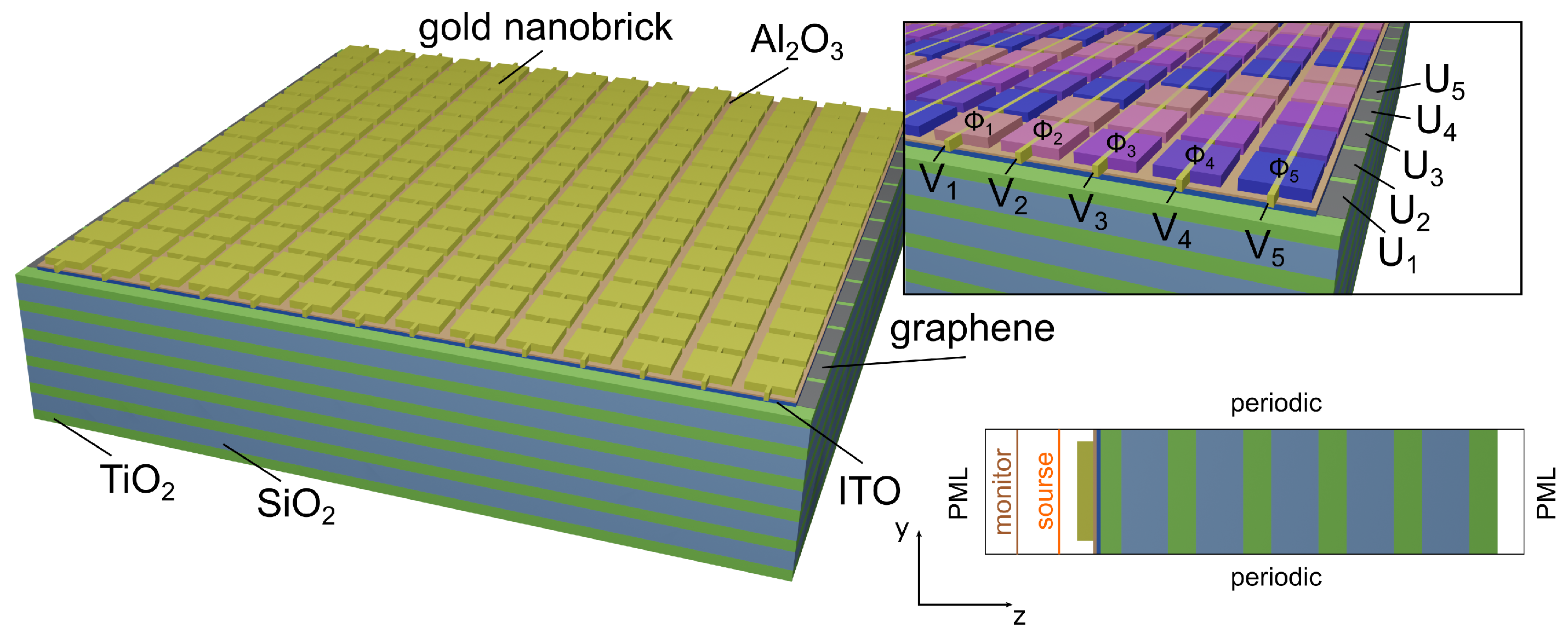
Figure 2.
(a) The real part of the dielectric permittivity of the ITO layer for different applied bias voltage. (b) Reflectance spectra of the bare PhC and metasurface. (c) Reflectance spectra of the structure presented in Figure 1. (d) Distribution of the refractive index and local field intensity in the structure at the TPP wavelength ( nm) at a bias voltage of 4 volts. (e) Simulated phase shift as a function of applied bias voltage between Au nanostripes and monolayer graphene. The results presented in (a,e) subplots were obtained for fixed wavelength at 1550 nm. The legend on subplot (a) is relevant for subplots (c,e).
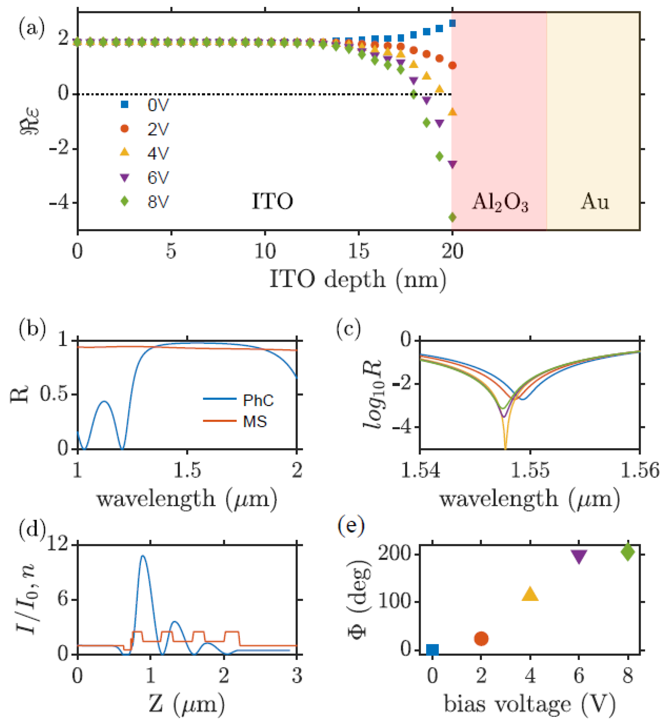
Figure 3.
Phase distribution along metasurface and far field intensity for different values and . In this case, , , are ordinal numbers of nanobricks along x and y-direction, respectively.
Figure 3.
Phase distribution along metasurface and far field intensity for different values and . In this case, , , are ordinal numbers of nanobricks along x and y-direction, respectively.
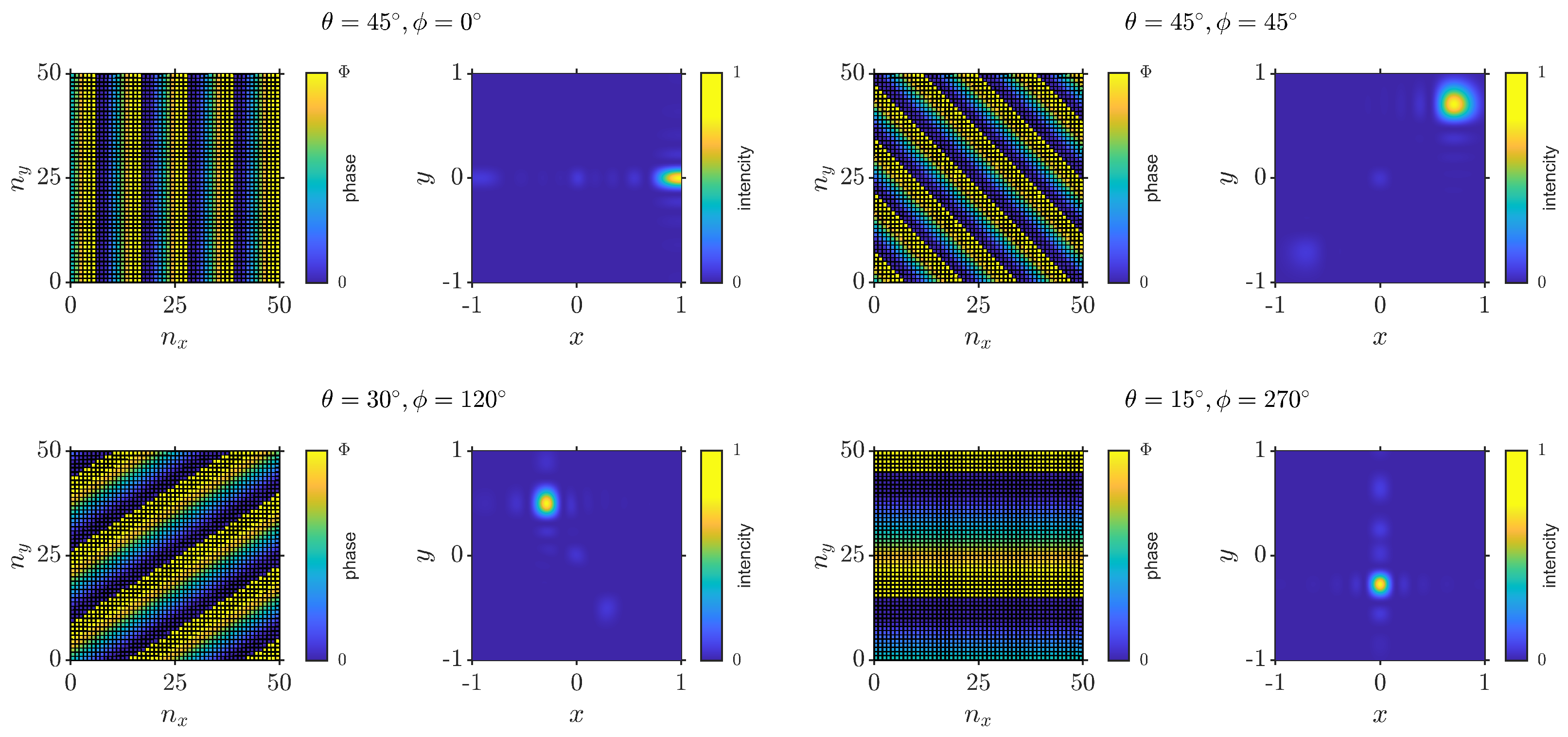
Figure 4.
Phase distribution along metasurface and far field intensity for different values and and contact numbers. In this case, , .
Figure 4.
Phase distribution along metasurface and far field intensity for different values and and contact numbers. In this case, , .
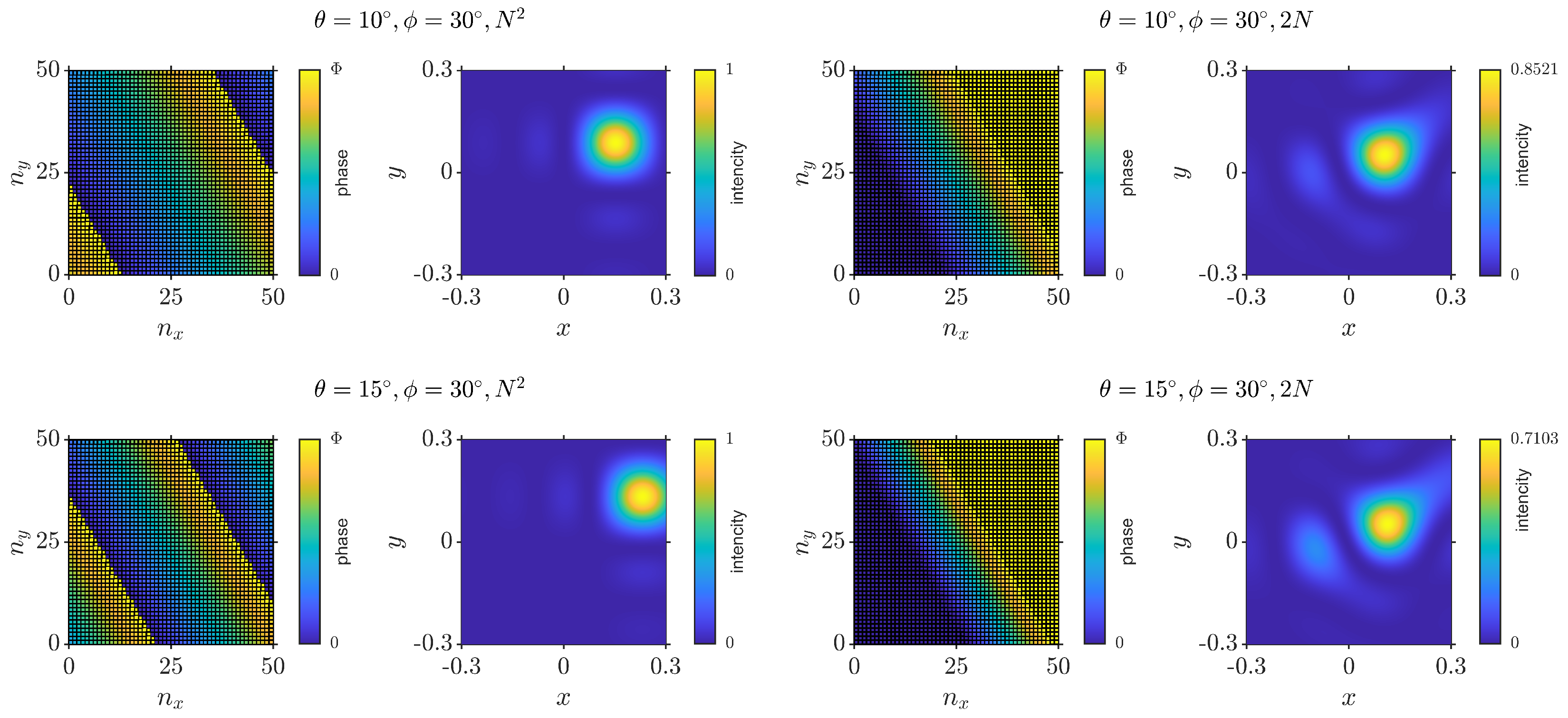
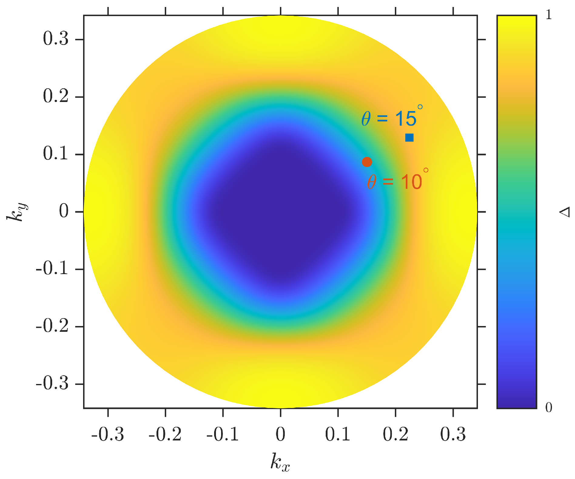
Figure 5.
for the proposed structure. In this case , .

Table 1.
Drude parameters for ITO.
| Carrier density, N (cm) | 2.2918 × 10 |
| Damping constant, (Hz) | 1.7588 × 10 |
| High-frequency permittivity, | 4.2345 |
| Effective mass, | 0.2525 |
Disclaimer/Publisher’s Note: The statements, opinions and data contained in all publications are solely those of the individual author(s) and contributor(s) and not of MDPI and/or the editor(s). MDPI and/or the editor(s) disclaim responsibility for any injury to people or property resulting from any ideas, methods, instructions or products referred to in the content. |
© 2023 by the authors. Licensee MDPI, Basel, Switzerland. This article is an open access article distributed under the terms and conditions of the Creative Commons Attribution (CC BY) license (https://creativecommons.org/licenses/by/4.0/).
Share and Cite
MDPI and ACS Style
Bikbaev, R.G.; Chen, K.-P.; Timofeev, I.V. Two-Dimensional Dynamic Beam Steering by Tamm Plasmon Polariton. Photonics 2023, 10, 1151. https://doi.org/10.3390/photonics10101151
AMA Style
Bikbaev RG, Chen K-P, Timofeev IV. Two-Dimensional Dynamic Beam Steering by Tamm Plasmon Polariton. Photonics. 2023; 10(10):1151. https://doi.org/10.3390/photonics10101151
Chicago/Turabian StyleBikbaev, Rashid G., Kuo-Ping Chen, and Ivan V. Timofeev. 2023. "Two-Dimensional Dynamic Beam Steering by Tamm Plasmon Polariton" Photonics 10, no. 10: 1151. https://doi.org/10.3390/photonics10101151
Note that from the first issue of 2016, this journal uses article numbers instead of page numbers. See further details here.