1. Introduction
Si photonics is an enabler of electronic and photonic integration on a Si CMOS (complementary metal oxide semiconductor) platform for cost-effective, bandwidth-abundant computation and communication on-chip networks. The current device challenge in Si photonics is the optical modulator to reduce the power consumption. Electro-refraction modulators (ERMs) such as Mach-Zehnder Interferometer (MZI) modulators [
1,
2] reported high power consumption in the order of ~pJ/bit because of the plasma effect that takes place to achieve the refractive index change of the long waveguide arm. Another type of ERM is ring resonator modulators [
3,
4], which do not require high power to operate but do require thermal management to match the resonance with the modulation wavelength. In contrast, electro-absorption modulators (EAMs) are essentially free from large power consumption because of the operation under reverse bias. The EAMs reported so far are based on the Franz-Keldysh effect of GeSi and Ge [
5,
6,
7,
8,
9,
10,
11] and the quantum confined Stark effect of SiGe/Ge quantum wells [
12,
13]. The current challenge in EAMs is to expand their operation wavelength range,
i.e., currently only ~10 nm with a reasonable extinction ratio (~10 dB). Since the range is limited by the fundamental absorption edge, Ge alloying with Si [
7] and stress-compressive Ge [
11] can tune the operation wavelength of EAMs to 1550 nm. However, the range of the operation wavelength remained unchanged in these approaches.
The present paper has demonstrated dynamic tuning of the fundamental absorption edge of Ge waveguides in terms of applying stress in Ge waveguides on a Si beam (cantilever). The stress tuning concept was applied in the three-dimensional microelectro-mechanical systems (MEMS)-based beam structures and the bandgap shifts from applying stress were detected by the photoluminescence peak shifts [
14,
15,
16,
17,
18]. To apply the concept to expand the range of the operation wavelength in terms of external stress, Ge waveguides are designed to be implemented on a Si waveguide on the Si beam. The devices have demonstrated ~40 nm red-shifts in the fundamental absorption edge of the Ge waveguides by dynamic external forces up to ~1 GPa on the Si beam. The shifts were consistent with the deformation potential calculations taking the propagation mode in the Ge waveguide into account. This prototype should be an enabler of the Ge EAMs with reconfigurable wavelength in the whole C-band in terms of external dynamic stressing.
2. Design of Ge Waveguide to Tune the Fundamental Absorption Edge
To design the Ge waveguide on a MEMS-based Si beam, the structure should be optimized to meet both optical and mechanical requirements. In this chapter, the design is optimized in terms of controlling the fundamental absorption edge via stress, the structure of the Ge waveguide on the Si beam, and the mode of propagation.
2.1. Design of the Fundamental Absorption Edge and Stress
The dependence of the fundamental absorption edge of the Ge waveguide on one-dimensional stress along the <110> direction is calculated on the basis of deformation potential theory [
18] as shown in
Figure 1. The reason to choose the direction is related to Ge epigrowth and is discussed later. Built-in two-dimensional tensile stress is accumulated in the Ge epilayer grown on Si, and it splits the valence band into heavy hole (HH) and light hole (LH) even at no <110> stress [
14]. Here, Γ-HH (Γ-LH) denotes the electron transition from the top of the HH (LH) band to the bottom of the Γ valley. It is clear that both Γ-HH and Γ-LH show “red-shifts” when one-dimensional tensile stress is applied to Ge. This indicates that the fundamental absorption edge of a Ge waveguide should be dynamically tuned depending on the amount of stress applied.
2.2. Design of Ge Waveguide on Si Beam Structure and Stress
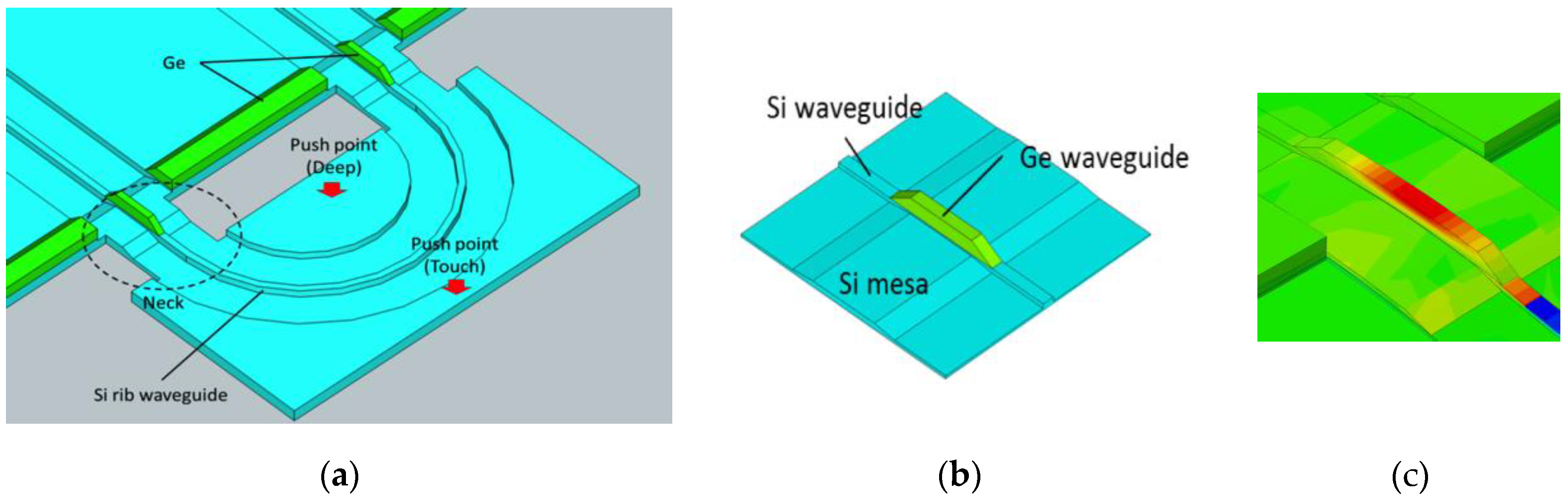
The structure of the Ge waveguide on the Si beam and its effective stressing are described. Finite domain time difference (FDTD) simulations are used to design single mode Ge waveguides on the beam, as schematically shown in
Figure 2: a 5-µm-long, 400-nm-thick and 400-nm-wide Ge waveguide on a Si rib waveguide with a 150 nm rib top on the Si on the insulator (SOI) wafer. The SOI wafer has a 250-nm-thick top Si layer on a 3-µm-thick buried oxide (BOX) layer. Here, the Si rib waveguide is employed to mechanically support the waveguide after removing the BOX layer under the Si beam. Employing the rib structure makes the bending radius of the Si waveguide large to minimize radiation losses. The 150-nm-high Si rib waveguide allows a bending radius of 10 μm which remains lower than 0.1 dB at the right angle bend, based on mode solver simulations. Based on these optimizations, our design of the Si beam to implement the Si rib waveguide should be 30 μm wide and 20 μm long. Such a large beam structure requires a specific design for effective stressing of the Ge waveguide. The neck structures as shown in
Figure 2a are to enhance the stress to the Ge waveguide on the wide beam. The finite element method simulation of stress is performed to optimize the neck to be 5 μm wide and 5 μm long in shape and it indicates the amount of tensile stress to the Ge waveguide should be as high as 1 GPa when bent down to the base Si.
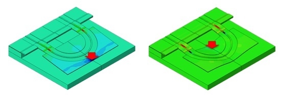
The finite element method (FEM) reveals the stress distribution in the Ge waveguide on the neck, as shown in
Figure 2c. The stress should have a linear depth profile, and thus the top of the Ge waveguide has the highest stress (red) and the bottom has the lowest (green).
The stresses at the typical point of the Ge waveguide are qualitatively shown in
Table 1 by taking reference points such as “Ge top”, a half-point of the thickness as “Ge middle”, and the interface between Ge and Si as “Ge bottom”. Here, an external force is applied at “Touch” and “Deep” until the beam touches down to the base Si. It has a peak near the waveguide direction. Here, the propagation mode would be the TE mode and the mode field is the highest near the Ge middle in steady state. Thus, the calculated amounts of stress at the Ge middle should be 0.2 and 1.3 GPa when applying stress to “Touch” and “Deep” and, needless to say, 0 GPa at “No stress”. These stress amounts are taken at the peak point along the wavelength direction. The predicted fundamental absorption edges are calculated, using
Figure 1, some of which are shown in
Table 1: referencing the Ge middle point at “No stress”, the red-shifts of Γ-HH should be 15 nm at “Touch” and 90 nm at “Deep”, while those of Γ-LH should be 35 nm at “Touch” and 200 nm at “Deep”.
2.3. Design of Propagation Mode in the Ge Waveguides
The coupling points of the Ge waveguide with the Si rib waveguide are shown in
Figure 2 and
Figure 3. The wedge-shaped Ge waveguide coupling with the Si rib waveguide should virtually generate a graded index structure to avoid unwanted scattering loss in terms of a sudden index change that the propagation mode experiences. It has so far been assumed that the propagation mode in the Ge waveguide should be in steady state. However, FDTD simulations of the mode propagation in the Ge and Si waveguide coupling indicate that the propagation mode is not in steady state but is transient in the 5-µm-long Ge waveguide, as shown in
Figure 3. In other words, the mode bounces ups to the Ge middle and down to the Ge bottom or the Si rib underneath. Accordingly, the propagation mode should experience an in-depth profile of the stress field accumulated in the Ge waveguide, as shown in
Figure 2c.
Considering that the propagation mode is transient, the transmittance T of the mode through the Ge waveguide should be expressed by:
Here,
denotes the incoming power of the propagation mode into the Ge waveguide,
the absorption coefficient given in the
Appendix,
the stress in the Ge waveguide as a function of the length (
x) and the height (
z) of the waveguide, as shown in
Figure 2c, and
the trajectory of the propagating mode in the Ge waveguide, as shown in
Figure 3. The rigorous solution of the transmittance has not been obtained from Equation (1), but the red-shift amount at the Ge bottom would be smaller than the prediction in
Table 1. We will discuss on it later in
Section 5.
3. Fabrication of Ge Waveguide on the Si Beam
Fabrication of the 20 30 µm beam ends up with a large removal of the surrounding BOX layer under the Si slab. A hydrofluoric acid (HF) solution is used to etch the BOX layer under the Si beam, which also removes the same amount of the BOX layer under the Si slab, referred to as the “undercut”. Bending the beam with a large undercut defocuses stress through the whole structure on the undercut and stress on the Ge waveguide is reduced. To make the undercut small, the beam is designed with many small through-holes 0.5 µm in diameter and arrayed every 2.5 µm in a square lattice. FDTD simulations suggest that the propagation mode in the Si rib waveguide would couple to the top of the base Si wafer, when the beam touches down to the base Si, coupling in radiation mode. To isolate the propagation mode even at touching down, the BOX layer is partially left at the top of the base Si, and thus SiO2 prevents the propagation mode from coupling to the base Si.
To achieve the wedge-shaped Ge waveguide edges, selective epitaxial growth (SEG) of Ge on Si has been used. The <311> faceted mesas on the sidewalls appear at the edge of the SEG Ge, which aligned to the {110} planes. The angle between the facet and (100) plane is 25.2°, which should be small enough to form graded index structures at the Ge waveguide, as shown in
Figure 3. Thus, the stressing direction should also be in parallel to the <110> directions, as shown in
Figure 1.
The Ge waveguides at the Si beam necks were devised on the top Si layer, using electron beam lithography and reactive ion etching. The 400-nm-thick Ge layer was first grown by an ultra-high-vacuum chemical vapor deposition method. A SiO2 layer was used as the SEG Ge mask to form (311) faceted wedge-shaped Ge waveguide edges. Reactive ion etching was performed by a Cl2 and O2 gas mixture plasma to fabricate a 400-nm-thick Ge waveguide and 150-nm-thick Si rib waveguide.
4. Results and Analyses
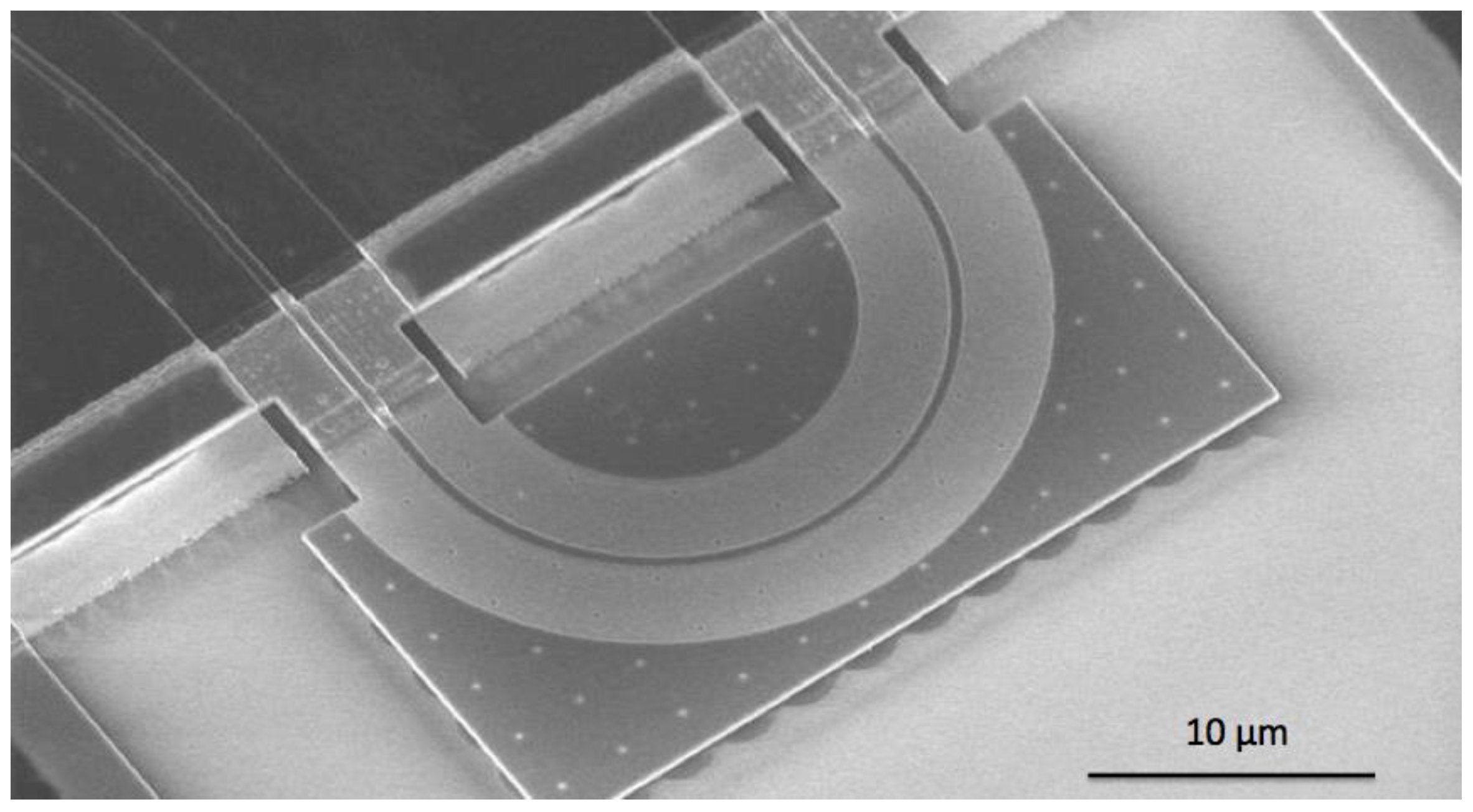
Figure 4 shows a typical SEM micrograph of the fabricated Si beam. The Si beam with two necks, the Si rib waveguide with a 10 µm bending radius on the beam, and two Ge waveguides on the Si rib waveguide on the necks are clearly shown, as designed. The white “dot” array on the beam is the through-holes to remove the BOX layer for fabrication of the free-standing beam and to maintain a thin SiO
2 layer under the beam for optical isolation.
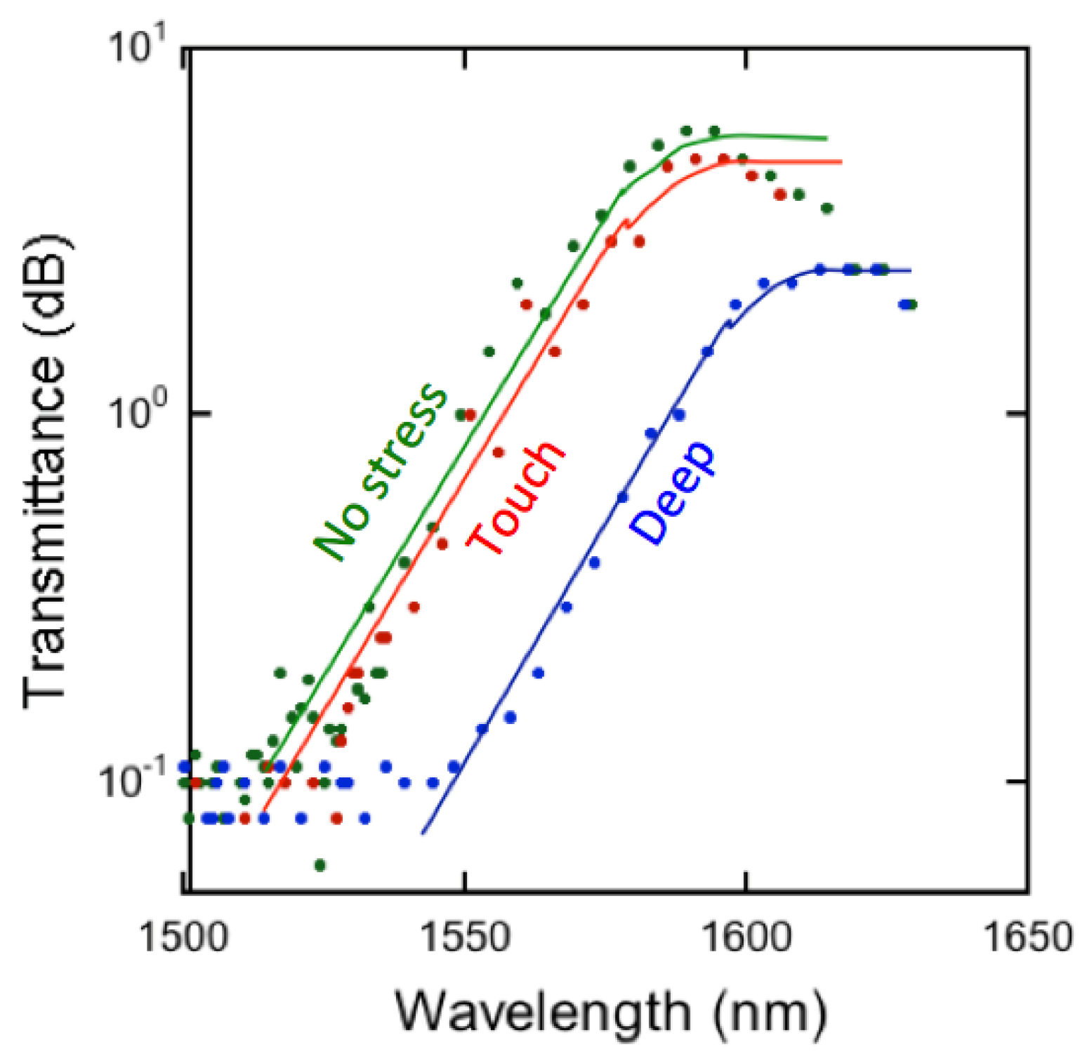
Figure 5 shows transmission spectra of the Ge waveguide under no stress (green) applied to it other than that applied to the “Touch” (red) and “Deep” (blue) points, as defined in
Figure 1a. The curve fittings are performed based on the calculation of the absorption coefficient, due to the Ge indirect bandgap that is calculated using one phonon model [
19]. The details are described in the
Appendix. The fittings well reproduce the experiment results, where the temperature-dependent constant at 291 K is used at 1900 cm
−1 for the best fits shown in the
Appendix. It is experimentally shown from the results that the red-shift by stressing is ~7 nm at “Touch”, and ~52 nm at “Deep”, assuming 2 × 5-µm-long Ge waveguides on the necks. Here, the beam was bent by applying an external force to touch down to the base Si to get these red-shifts. The absorption curve at “No stress” was used as the reference.
These observations indicate that the absorption edge at the propagation mode is to experience is Γ-HH as shown in
Figure 1. It may be fair to exclude Γ-LH since the red-shifts are too large (35 nm and 200 nm at the “Touch” and “Deep” points). The red-shifts by Γ-HH as shown in
Table 1 are 15 nm and 90 nm at stressing the “Touch” and “Deep” points, which are twice larger compared with the observations. The discrepancy is due to the fact that the propagation mode is transient and the stress profiles in the depth and along the waveguide are inhomogeneous. It is rather hard to predict how the transmission will behave. We will come back to this point in the discussion. Here, it is concluded that applying dynamic stress to the Ge waveguide on the Si beam could precisely tune its fundamental absorption edge at any wavelength in the range of 40 nm. In other words, Ge EAMs, if fabricated on the beam, will cover the entire C-band range (35 nm) in the optical communication wavelength by dynamic stressing at the “Deep” point.
5. Discussion
To understand the discrepancy between experimental transmittances in
Figure 5 and theoretical predictions made by Equation (1), first we should assume that the trajectory of the propagating mode in the Ge waveguide does not change upon the strength of stressing. In other words, it is always the same as the one shown in
Figure 3. We can define
in Equation (1) as a sinusoidal curve; the period along the
x direction is 2 µm and the intensity is half of the Ge waveguide height (H) with z = 0 at the Ge and Si interface. We further assume that the stress along the Ge waveguide direction is uniform although actual distribution exists, as shown in
Figure 2c. This leads us to express Equation (1) as:
Here,
is the maximum stress the mode field experiences depending on the stress point. The point should be the Ge middle. A simple calculation using Equation (2) showed us that the red-shift of the fundamental absorption edge becomes 7.5 nm at “Touch” and 45 nm at “Deep”. These agree with the observed red-shifts in
Figure 5,
i.e., ~7 nm at “Touch” and 52 nm at “Deep”, despite the fact that the non-uniformity of stress along the Ge waveguide direction as shown in
Figure 2c is ignored in this calculation. This leads us to conclude that the discrepancy between the predicted red-shifts in
Table 1 and the observed ones in
Figure 5 should be induced by the transient propagation mode in the Ge waveguides.
The transmittance results in
Figure 5 show clear reductions at the wavelength range beyond 1600 nm, despite the fact that the theoretical curves do not show such decreases. The difference can also be explained by the transient propagation mode in
Figure 3. The propagation mode smoothly couples down to the Si rib waveguide as shown in
Figure 5. It should be noted that the wavelength is 1550 nm in the FDTD simulations. The propagation mode should hit the (311) Ge waveguide wedge when the wavelength becomes different from 1550 nm. This is the reason why the transmittance is reduced beyond 1600 nm. Such a reduction should have happened to the wavelength range around 1500 nm. However, the intensities of the transmittance are below the noise level of these measurements and thus it is not detectable.
Finally, it should be proposed that the stress tuning of the Ge waveguide could be done using an electrostatic force applying a voltage across the beam and the base Si wafer [
20]. By fabricating an electrode at “Deep” on the Si beam and applying a voltage across the electrode and the base Si to touch the “Deep” point down to the base Si, the 52 nm red-shift should be reproduced. In this configuration, the SiO
2 layer intentionally left on the base Si should work for isolating the Si beam not only optically but also electrically from the Si wafer.
6. Conclusions
The present paper has proposed a way to dynamically tune the fundamental absorption edge of Ge waveguides by applying tensile stress to them and it described a prototype Ge waveguide on a Si beam structure. The three-dimensional structures of microelectro-mechanical systems (MEMS)-based Ge waveguide on a Si beam are optimized in terms of stress, mechanical stability, and propagation mode and then fabricated. It has been demonstrated that the absorption edge of two Ge waveguides on the Si beam can be dynamically tuned to show the red-shift in the wavelength range of ~52 nm by applying an external force of 1 GPa to the “Deep” point of the Si beam. The experimentally observed red-shifts are well explained, considering the transient mode of propagation in the Ge waveguides. The presented dynamic tuning method should enable the reconfiguration of the operation wavelength range of Ge electro-absorption modulators in the entire C-band. We propose that an electro-static force can be applied to achieve on-chip stress tuning devices in practical applications.
Supplementary Files
Supplementary File 1Acknowledgments
This research project was partly supported by the Ministry of Education, Culture, Sports, Science and Technology (MEXT), Japan (Nanotechnology Platform, Project No. 12024046).
Author Contributions
M.H. and L.M.N. designed and performed the experiments; H.F. performed electro-static tuning experiment; Y.I. and K.W. co-supervised the studies.
Conflicts of Interest
The authors declare no conflict of interest.
Appendix
In the one phonon model [
19], the indirect absorption has the quadratic dependence in the energy difference between the photon energy on one hand and the band gap energy plus or minus phonon energy.
Here,
A denotes a temperature-dependent constant (cm
−1),
the phonon energy,
the energy of the photon,
the indirect band gap (0.664 eV) and
T the temperature in Kelvins. For simplicity, we use the longitudinal acoustic phonon of Ge with the energy of 27.7 meV. The built-in stress in the Ge epilayer on Si splits the valence band into the
LH and the
HH band, as in
Figure 1. The contribution of each indirect band to the total absorption,
, depends on the effective masses and can be formulated as follows:
where
,
,
, and
. The electron mass at
L valley
is 0.22 m
o. Using Equations (A1) and (A2), we obtained
Figure 4 to fit the experimental data.
References
- Green, W.M.; Rooks, M.J.; Sekaric, L.; Vlasov, Y.A. Ultra-compact, low RF power, 10 Gb/s silicon Mach-Zehnder modulator. Opt. Express 2007, 15, 17106–17113. [Google Scholar] [CrossRef] [PubMed]
- Reed, G.T.; Mashanovich, G.; Gardes, F.Y.; Thomson, D.J. Silicon optical modulators. Nat. Photonics 2010, 4, 518–526. [Google Scholar] [CrossRef] [Green Version]
- Xu, Q.; Schmidt, B.; Pradhan, S.; Lipson, M. Micrometre-scale silicon electro-optic modulator. Nature 2005, 435, 325–327. [Google Scholar] [CrossRef] [PubMed]
- Watts, M.R.; Zortman, W.A.; Trotter, D.C.; Young, R.W.; Lentine, A.L. Vertical Junction silicon microdisk modulators and switches. Opt. Express 2011, 22, 21989–22003. [Google Scholar] [CrossRef] [PubMed]
- Jongthammanurak, S.; Liu, J.F.; Wada, K.; Cannon, D.D.; Danielson, D.T.; Pan, D.; Kimerling, L.C.; Michel, J. Large Electro-optic Effect in Tensile Strained Ge-on-Si Films. Appl. Phys. Lett. 2006, 89. [Google Scholar] [CrossRef]
- Liu, J.F.; Pan, D.; Jongthammanurak, S.; Wada, K.; Kimerling, L.C.; Michel, J. Design of monolithically integrated GeSi electro-absorption modulators and photodetectors on a SOI platform. Opt. Express 2007, 15, 623–628. [Google Scholar] [CrossRef] [PubMed]
- Liu, J.F.; Beals, M.; Pomerene, A.; Bernardis, S.; Sun, R.; Cheng, J.; Kimerling, L.C.; Michel, J. Waveguide integrated, ultra-low energy GeSi electro-absorption modulators. Nat. Photonics 2008, 2, 433–437. [Google Scholar] [CrossRef]
- Lim, A.E.; Liow, T.; Qing, F.; Duan, N.; Ding, L.; Yu, M.; Lo, G.; Kwong, D.-L. Novel evanescent coupled germanium electro absorption modulator featuring monolithic integration with germanium PIN photodetector. Opt. Express 2010, 19, 5040–5046. [Google Scholar] [CrossRef] [PubMed]
- Feng, N.N.; Feng, D.; Liao, S.; Wang, X.; Dong, P.; Liang, H.; Kung, C.C.; Qian, W.; Fong, J.; Shafiiha, R.; et al. 30 GHz Ge electro-absorption modulator integrated with 3 μm silicon-on-insulator waveguide. Opt. Express 2011, 19, 7062–7067. [Google Scholar] [CrossRef] [PubMed]
- Feng, D.; Liao, S.; Liang, H.; Fong, J.; Bijlani, B.; Shafiiha, R.; Luff, B.J.; Luo, Y.; Cunningham, J.; Krishnamoorthy, A.V.; et al. High speed GeSi EA modulator at 1550 nm. Opt. Express 2012, 20, 22224–22232. [Google Scholar] [CrossRef] [PubMed]
- Nguyen, L.M.; Kuroyanagi, R.; Tsuchizawa, T.; Ishikawa, Y.; Yamada, K.; Wada, K. Stress tuning of the fundamental absorption edge of pure germanium waveguides. Opt. Express 2015, 23, 18487–18492. [Google Scholar] [CrossRef] [PubMed]
- Kuo, Y.-H.; Lee, Y.K.; Ge, Y.; Ren, S.; Roth, J.E.; Kamins, T.I.; Miller, D.A.B.; Harris, J.S. Quantum-confined stark effect in Ge-SiGe quantum wells on Si for optical modulators. IEEE J. Sel. Top. Quantum Electron. 2006, 12, 1503–1513. [Google Scholar] [CrossRef]
- Chaisakul, P.; Marris-Morini, D.; Roulfed, N.-S.; Frigerio, J.; Charastina, D.; Coudevylle, J.-P.; Roux, X.L.; Edmong, S.; Isella, G.; Vivien, L. Recent Progress in GeSi electro-absorption modulators. Sci. Technol. Adv. Mater. 2014, 15, 14601–14608. [Google Scholar] [CrossRef]
- Ishikawa, Y.; Wada, K.; Cannon, D.D.; Liu, J.; Luan, H.-C.; Kimerling, L.C. Strain-induced band gap shrinkage in Ge grown on Si substrate. Appl. Phys. Lett. 2003, 82. [Google Scholar] [CrossRef]
- Yoshimoto, K.; Suzuki, R.; Ishikawa, Y.; Wada, K. Bandgap control using strained beam structures for Si photonic devices. Opt. Express 2010, 18, 26492–26498. [Google Scholar] [CrossRef] [PubMed]
- Cai, J.; Ishikawa, Y.; Wada, K. Strain induced bandgap and refractive index variation of silicon. Opt. Express 2013, 21, 7162–7170. [Google Scholar] [CrossRef] [PubMed]
- Horie, Y.; Decostered, L.; Suzuki, R.; Ishikawa, Y.; Wada, K. Emission wavelength tuning by mechanical stressing of GaAs/Ge/Si microbeams. Opt. Express 2011, 19, 15732–15738. [Google Scholar] [CrossRef] [PubMed]
- Wada, K.; Yoshimoto, K.; Horie, Y.; Cai, J.; Lim, P.H.; Fukuda, H.; Suzuki, R.; Ishikawa, Y. Srtrained Ge for Si-Based Integrated Photonics. In Photonics and Electronics with Ge; Wada, K., Kimerling, L.C., Eds.; Wiley-VHC: Weinheim, Germany, 2015; p. 219. [Google Scholar]
- Macfarlane, G.G.; Roberts, V. Infrared Absorption of Germanium near the Lattice Edge. Phys. Rev. 1955, 97. [Google Scholar] [CrossRef]
- Fukuda, H. A Study of Silicon Microphotonics for Telecommunication Applications. Ph.D. Thesis, the University of Tokyo, Tokyo, Japan, 2014. [Google Scholar]
© 2016 by the authors; licensee MDPI, Basel, Switzerland. This article is an open access article distributed under the terms and conditions of the Creative Commons by Attribution (CC-BY) license (http://creativecommons.org/licenses/by/4.0/).


