Article

Spectroscopic Properties of Gold Curvilinear Nanorod Arrays

1
Metamaterials Laboratory, RIKEN, 2-1 Hirosawa, Wako, Saitama 351-0198, Japan
2
RIES, Hokkaido University, N21W10, Kita-Ward, Sapporo, Hokkaido 001-0021, Japan
3
Department of Innovative and Engineered Materials, Tokyo Institute of Technology, 4259 Nagatsuta, Yokohama, Kanagawa 226-8503, Japan
4
Innovative Photon Manipulation Research Team, RIKEN Center for Advanced Photonics, RIKEN, 2-1 Hirosawa, Wako, Saitama 351-0198, Japan
*
Author to whom correspondence should be addressed.
Photonics 2016, 3(2), 18; https://doi.org/10.3390/photonics3020018
Submission received: 4 March 2016 / Revised: 2 April 2016 / Accepted: 4 April 2016 / Published: 8 April 2016
(This article belongs to the Special Issue 3D- and 2D-Nanofabrication for Photonic Devices)

Abstract

:
We designed and fabricated gold curvilinear nanorod periodical arrays using microfabrication techniques. The gold curvilinear nanorods had two distinct resonant peaks in the near-infrared region between 1630 nm and 3000 nm. Similar peak was observed in gold straight nanorods at specific lengths. At lengths identical to the arc length of the curvilinear nanorod, the peak was in the relative range of 3000 nm, which corresponds to the longitudinal plasmon mode (L-mode). At lengths identical to half of the arc length of the curvilinear nanorod, the peak was close to 1630 nm. Plasmon resonant peaks were tunable in the infrared region by changing the arc length of the curve, the line width, and distance between the curvilinear nanorods. In particular, when two curvilinear nanorods were closely packed in a range of less than 100 nm, the peak wavelength of curvilinear nanorod was shifted due to the plasmonic coupling of each mode.

Graphical Abstract

1. Introduction

Local-mode surface plasmon (LSP) resonances are collective oscillations of free electrons in noble metal nanostructures that give rise to strong resonant scattering of the incident radiation and localization of the electromagnetic field in the vicinity of the nanoparticles’ surface. Thus far, there are numerous reports that the LSP spectral properties of nanorods and nanoparticles are closely related to their size, shape, and distance between nanostructures [1,2,3,4,5]. Recently, considerable attention has been given to regulating these parameters for applications in metamaterials [6,7] and highly sensitive biological sensors [8,9]. One such example is the observation of Fano resonances though position placement of nanorods [10,11,12] and nanodots [13,14]. However, there are only a few reports [15,16] on the spectral properties of LSP in intricately-shaped metal structures, including metal curve-shaped nanorods.
In this work, we focus on the plasmon resonance of a curve-shaped nanorod. We investigated the LSP spectral properties of gold curvilinear nanorods that were artificially designed curve geometry using microfabrication techniques.

2. Experimental Section

2.1. Gold Nanorods Fabrication Process

The periodic arrays of gold nanostructures were fabricated on the glass substrate via electron beam lithography and lift-off technique. First, ZEP520A resist (Zeon Corporation, Chiyoda, Japan) was diluted with ZEP-A (Zeon Corporation) at a 1:2 volumetric ratio and was spin-coated on the substrate at 1000 rpm for 10 s and at 4000 rpm for 90 s to form a resist layer with a thickness of 130 nm. The resist was baked on a hot plate for 2 min at 180 °C. A water soluble conductive polymer called Espacer 300Z (Showa Denko K. K., Minato, Japan), which, for this study, acts as a charge-dissipating layer, was spin-coated on the resist at 1000 rpm for 10 s and at 4000 rpm for 60 s. High-resolution electron beam lithography (ELS-F125, ELIONIX INC., Hachioji, Japan) was conducted using an acceleration voltage of 125 kV, a beam current of 1 nA and an exposure dose of 300 μC/cm−2. Nanostructures were designed to have constant periodicity in two dimensions using computer-aided design software of the electron beam lithography system. The insulated resist was developed in methyl isobutyl ketone (Wako Pure Chemical Industries, Ltd., Osaka, Japan) for 45 s. Next, a 2-nm chromium and 40-nm gold bilayer was deposited by helicon sputtering (MPS-4000, ULVAC, Inc., Chigasaki, Japan). The helicon sputtering system can sputter under high vacuum. The use of long distance sputtering and vertical incidence configuration is ideal for a flat and smooth film even in the nanopattern of the resist. Finally, the residual resist is removed by lift-off in an ultrasonic bath of ZDMAC (Zeon Corporation) solvent for 1 min. A scanning electron microscope (SEM: JSM-6700FT, JEOL Ltd., Akishima, Japan) was used to verify the structures’ shape and to measure the mean dimensions.

2.2. Measurement of Extinction Spectra

The optical properties of the fabricated nanostructures were characterized by their extinction spectra, which were measured using a commercially available Fourier-transform infrared (FT-IR) spectrometer equipped with a microscope attachment (FT/IR-6000TM-M, JASCO Corporation, Hachioji, Japan). The measured spectral range was from 800 nm to 4200 nm, and the measured sample area was about 20 μm × 20 μm, which corresponds to at least 2000 structures.

3. Results and Discussion

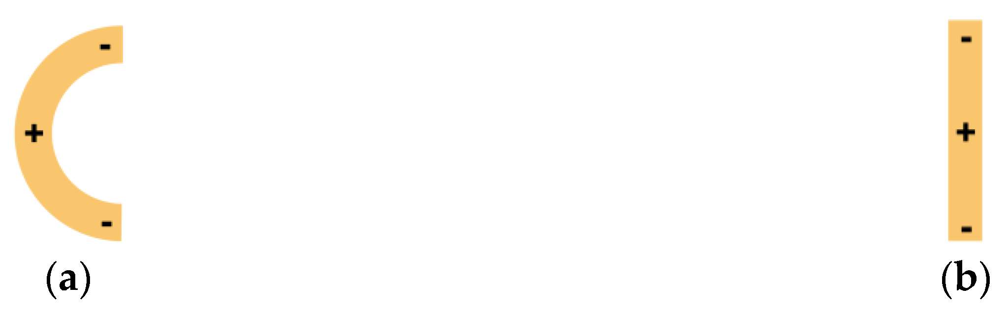
3.1. Plasmon Peak Assignment of Gold Curvilinear Nanorods

Figure 1a shows SEM images of the fabricated gold curvilinear nanorod array. Each curvilinear nanorod had parabolic shape and the following geometric parameters: height (h) = 622 nm, width (w) = 330 nm, arc length (l) = 890 nm, and line width (t) = 72 nm. The thickness of gold curvilinear nanorod is fixed at 40 nm. In addition to the curvilinear nanorods, gold straight nanorods were also fabricated having t = 72 nm and varying long axis length related to the dimensions of curvilinear nanorod in Figure 1a. The lengths of nanorods α, β, γ, and δ correspond to w = 330 nm, l/2 = 440 nm, h = 630 nm, and l = 890 nm, respectively (Figure 1b).
The extinction spectra of gold curvilinear nanorods shown in Figure 2a was that measured under the unpolarized light illumination, and Figure 2b and c are those under linearly polarized illumination. The extinction spectrum using unpolarized light (Figure 2a) has one peak at 1200 nm and two distinct peaks at 1630 nm and 3000 nm, which can be excited selectively depending on the polarization of the incident light, as shown in Figure 2b,c.
Figure 3 shows the extinction spectra of gold straight nanorods α, β, γ, and δ. Figure 3a shows the spectra under the x-direction polarized illumination. Straight nanorods (α) and (β) have only one peak in the infrared region, which originates from the long axis plasmon resonance (longitudinal mode, L-mode). For the y-direction polarized illumination, straight nanorods γ and δ have only one peak in the spectral range from 1000 to 4000 nm (Figure 3b). There are no observed extinction peaks for straight nanorods α and β in Figure 3b, and the same goes for γ and δ in Figure 3a in the infrared region. The short axis plasmon resonance (transverse mode, T-mode) was also observed at 530 nm in the visible region (data not shown).
Comparing the resonant peaks of both kinds of nanorods, the extinction peak of curvilinear nanorod in Figure 2c, when illuminated with linearly polarized light in the y-direction, is found around 3000 nm and is identical to that of straight nanorod δ in Figure 3b. In another case, the extinction peak of curvilinear nanorod, when illuminated with linearly polarized light in the x-direction, is around 1630 nm and is identical to that of straight nanorod β. Note that the length of straight nanorod δ is equal to the arc length of curvilinear nanorod (l). This indicates that free electrons moving along the curve-shaped nanorod feel the total arc length of the curve (l), not the projection length (h). Likewise, note that the length of straight nanorod β in Figure 3a is equal to half the arc length of curvilinear nanorod (l/2), not the width (w). The extinction peak of the curvilinear nanorod at 1630 nm in Figure 2b was attributed to the first plasmon mode due to the horizontal oscillation of free electrons, as shown in Figure 4a. By contrast, the same plasmon mode of the straight nanorod shown in Figure 4b is a forbidden mode (dark plasmon mode). The extinction peak at 1200 nm in Figure 2b was caused by the second plasmon mode due to the oscillation of free electrons for the x-direction polarized illumination.

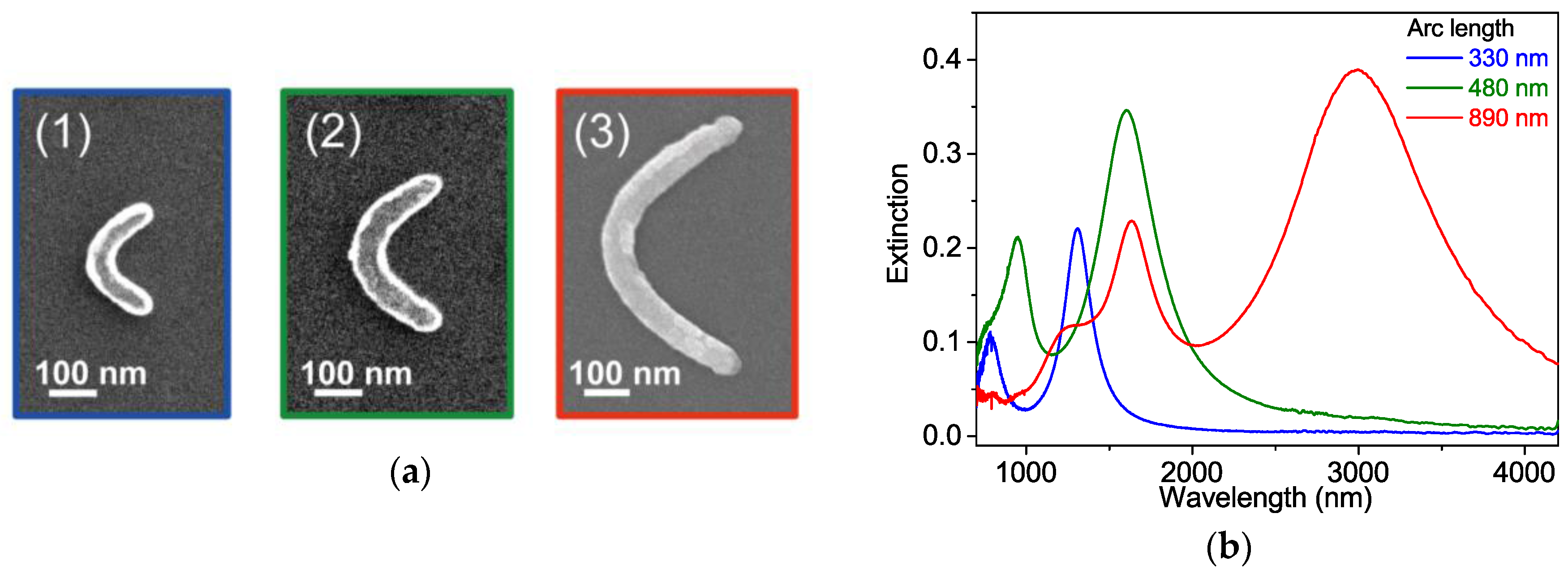
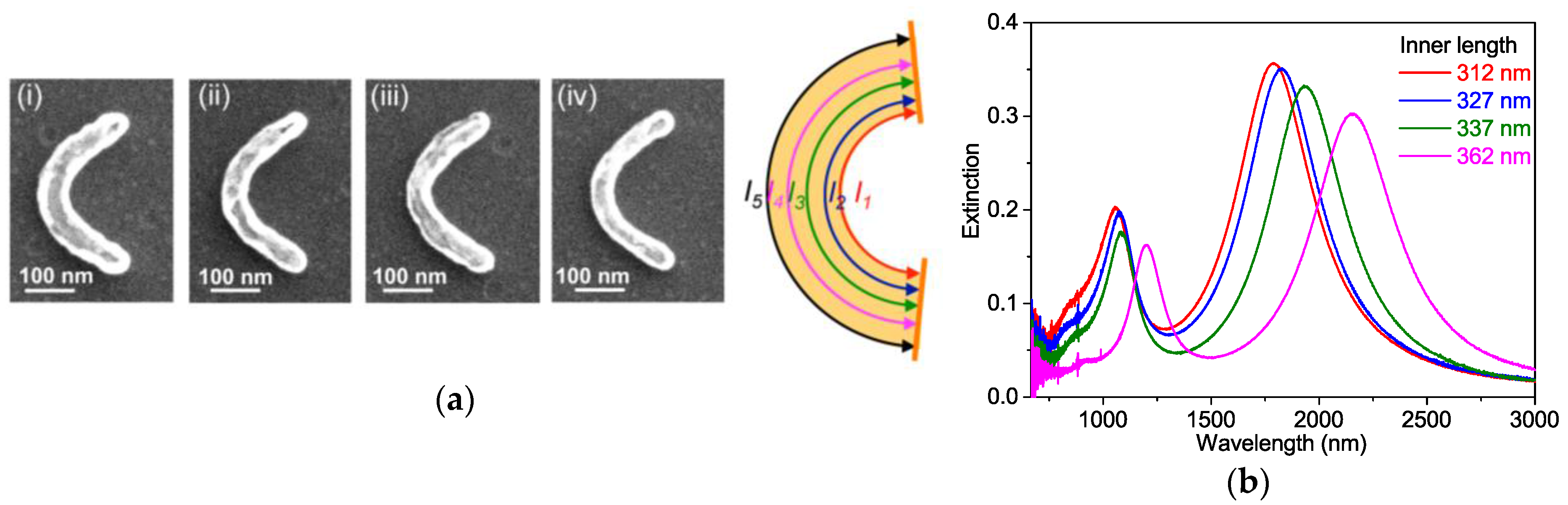
3.2. Plasmon Resonant Peak by Controlling Arc Length of Gold Curvilinear Nanorods

Three different arc lengths of the gold curvilinear nanorods were fabricated and their extinction spectra were measured under the unpolarized light illumination (Figure 5). The line widths (t) of all the structures are 72 nm. The arc lengths of the gold curvilinear nanorods were 330 nm, 480 nm, and 890 nm, respectively. When the arc length became long, both peaks of the gold curvilinear nanorods shifted to longer wavelengths. This result illustrates that it is possible to tune the plasmon peaks of curvilinear nanorods by changing the arc length.
The effect of changing the inner arc length while the outer arc length (l5) remained constant was also investigated (Figure 6). The fabricated inner arc lengths (l1–4) of the curvilinear nanorods were 312 nm, 327 nm, 337 nm, and 362 nm, respectively (Figure 6a). The outer arc length (l5) of the fabricated curvilinear nanorods (i)–(iv) was fixed at 476 nm. As the inner arc lengths were gradually increased, the two plasmon peaks were shifted to longer wavelengths as shown in Figure 6b. This result indicates that the inner arc length of the curve-shaped nanorods depends on the extinction peak wavelength.

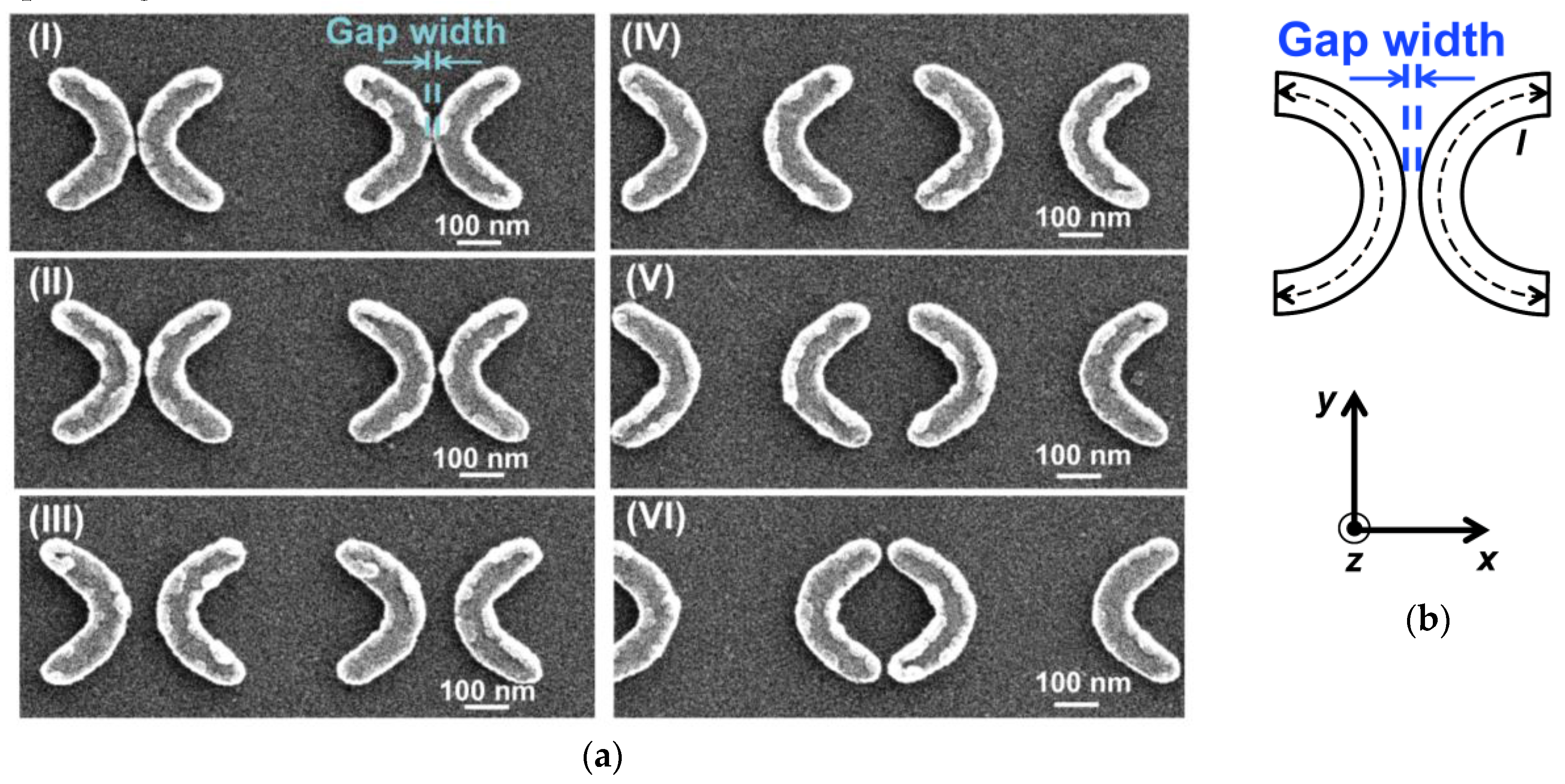
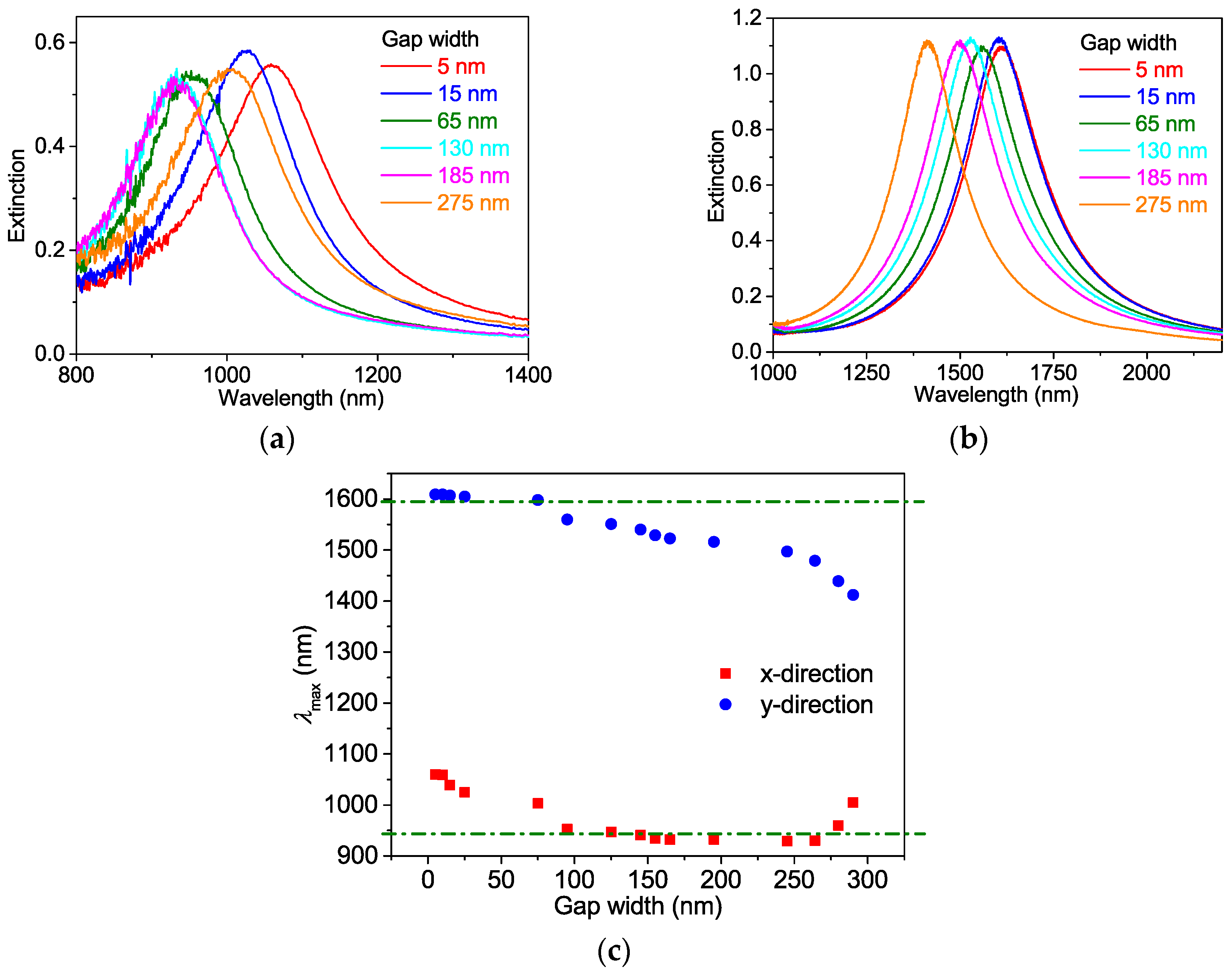
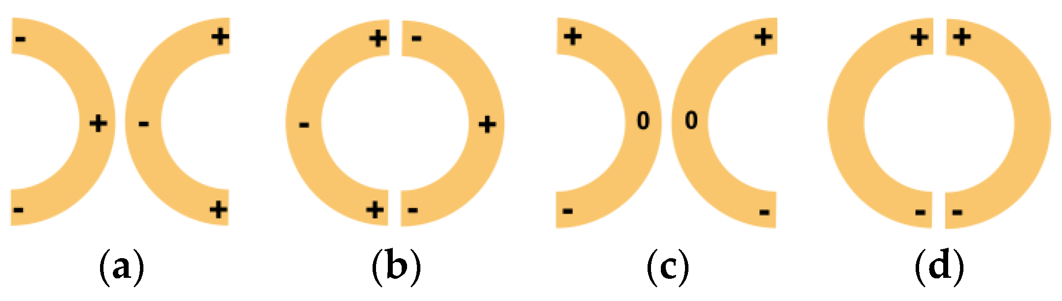
3.3. Plasmon Resonant Peak by Controlling Arrangement of Gold Curvilinear Nanorods

The LSP resonances of closely packed dimers consisting of two identical metal nanostructures strongly interact due to dipole-dipole coupling [17,18]. As shown in Figure 7a, y-axis symmetric curvilinear nanorod dimers with different gap widths were fabricated. In this experiment, the unit curvilinear nanorod is downsized and its size is the same as the one of Figure 5a (2). Based on the schematic of the dimer in Figure 7b, the gap width is defined as the distance between the outer curves of the nanorods. According to this definition, the gap widths of curvilinear nanorod dimers (I), (II), (III), (IV), (V), and (VI) are 5 nm, 15 nm, 65 nm, 130 nm, 185 nm, and 275 nm, respectively. As shown in Figure 7a (VI), when the gap width becomes wider, the dimer becomes similar to the split-ring resonator [19].
Figure 8a and b show extinction spectra of the dimer structures with respect to the x- and y-direction of linearly polarized light, respectively. In addition, to clarify the relationship between peak wavelength and gap width for both polarization directions, the plasmon peak positions were plotted in Figure 8c. Broken lines in Figure 8c indicate the plasmon peak wavelength of curvilinear nanorod monomers (Figure 5b, the arc length was 480 nm).
When linearly polarized light that oscillates in the x-direction illuminated on the gold curvilinear nanorod dimers, their extinction spectra had only one peak in the 900–1100 nm wavelength range. For 130 nm and 185 nm gap dimers, the plasmon peak wavelength was around 900 nm; which is almost the same as that of curvilinear nanorod monomer. When the gap distance becomes narrower or wider, the plasmon peak wavelength was red-shifted. This result can be explained that due to the plasmonic coupling of two curvilinear nanorods, the lower energy hybridized modes shown in Figure 9a,b were excited.
When the polarization direction of the incident light changed to the y-direction, the extinction spectra of dimers had one peak in the 1300–1700 nm wavelength region. In the range of gap distance of 5 to 100 nm, which means two curvilinear nanorods are facing their center portion with nanogap (Figure 7a (I)–(III)), the peak wavelength of extinction spectra were not changed. This can be understood that under the y-polarized illumination, fundamental L-mode (dipole mode) was excited in each nanorods, and at the nanogap position electric field becomes zero because it is node position as shown in Figure 9c. Therefore, even when two nanorods are closely packed with nanometer gap, there is almost no interaction between them and plasmon peak wavelength was not affected. When the gap distance increases, the dimer shape becomes single ring split-ring-resonator with two cuts, which means two nanorods are facing with their end points, and plasmon wavelength was dramatically blue-shifted. This is explained by the fact that, due to the resonant coupling of two nanorods, the higher energy hybridized mode shown in Figure 9d was excited.

4. Conclusions

We experimentally fabricated various size and shape of gold curvilinear nanorods and measured their extinction spectra. Fabricated gold curvilinear nanorods exhibited two characteristic peaks in the infrared region and can be easily distinguished by changing the polarization of the incident light. Tunability of the plasmon resonance peaks of the gold curvilinear nanorods by controlling the arc length was demonstrated. This experimental result showed that the plasmon peak wavelength is governed by the size of the inner arc length of the nanorods when the outer arc lengths of the curvilinear nanorods were fixed. For y-symmetric curvilinear nanorod dimers, the degree of resonant coupling depends on its configuration. Two curvilinear nanorods were placed closing their node of the electric field distribution (Figure 7a (I)), almost there is no resonant coupling and the extinction peak was not shifted. On the other hand, two curvilinear nanorods placed facing their ends, the resonance peak was influenced and blue-shifted when they are packed with the gap less than 100 nm.

Acknowledgments

This work was supported by funding from the Ministry of Education, Culture, Sports, Science, and Technology of Japan: The Nanotechnology Platform (Hokkaido University) and the Low-Carbon Research Network of Japan.

Author Contributions

Y.Y., K.U., and H.M. have contributed to the fabrications. Y.Y. and T.T. have contributed to measurement of the spectra; T.T. have contributed to the theory and design of the structures. All authors contributed to writing the papers, arrangement, and contents of the manuscript.

Conflicts of Interest

The authors declare no conflict of interest.

Abbreviations

LSP
local-mode surface plasmon

References

  1. Perez-Juste, J.; Pastoriza-Santos, I.; Liz-Marzan, L.M.; Mulvaney, P. Gold nanorods: Synthesis, Characterization and Applications. Coordin. Chem. Rev. 2005, 249, 1870–1901. [Google Scholar] [CrossRef]
  2. Jain, P.K.; Lee, K.S.; El-Sayed, I.H.; El-Sayed, M.A. Calculated Absorption and Scattering Properties of Gold Nanoparticles of Different Size, Shape, and Composition: Applications in Biological Imaging and Biomedicine. J. Phys. Chem. B 2006, 110, 7238–7248. [Google Scholar] [CrossRef] [PubMed]
  3. Zhang, S.; Genov, D.A.; Wang, Y.; Liu, M.; Zhang, X. Plasmon-Induced Transparency in Metamaterials. Phys. Rev. Lett. 2008, 101, 047401. [Google Scholar] [CrossRef] [PubMed]
  4. Smythe, E.J.; Cubukcu, E.; Capasso, F. Optical Properties of Surface Plasmon Resonances of Coupled Metallic Nanorods. Opt. Express 2007, 15, 7439–7447. [Google Scholar] [CrossRef] [PubMed]
  5. Ueno, K.; Mizeikis, V.; Juodkazis, S.; Sasaki, K.; Misawa, H. Optical Properties of Nanoengineered Gold Blocks. Opt. Lett. 2005, 30, 2158–2160. [Google Scholar] [CrossRef] [PubMed]
  6. Shalaev, V.M.; Cai, W.; Chettiar, U.K.; Yuan, H.-K.; Sarychev, A.K.; Drachev, V.P.; Kildishev, A.V. Negative Index of Refraction in Optical Metamaterials. Opt. Lett. 2005, 30, 3356–3358. [Google Scholar] [CrossRef] [PubMed]
  7. Ishikawa, A.; Tanaka, T.; Kawata, S. Negative Magnetic Permeability in the Visible Light Region. Phys. Rev. Lett. 2005, 95, 237401. [Google Scholar] [CrossRef] [PubMed]
  8. Murphy, C.J.; Gole, A.M.; Stone, J.W.; Sisco, P.N.; Alkilany, A.M.; Goldsmith, E.C.; Baxter, S.C. Gold Nanoparticles in Biology: Beyond Toxicity to Cellular Imaging. Accounts. Chem. Res. 2008, 41, 1721–1730. [Google Scholar] [CrossRef] [PubMed]
  9. Chung, T.; Lee, S.-Y.; Song, E.Y.; Chun, H.; Lee, B. Plasmonic Nanostructures for Nano-Scale Bio-Sensing. Sensors 2011, 11, 10907–10929. [Google Scholar] [CrossRef] [PubMed]
  10. Verellen, N.; Sonnefraud, Y.; Sobhani, H.; Hao, F.; Moshchalkov, V.V.; van Dorpe, P.V.; Nordlander, P.; Maier, S.A. Fano Resonances in Individual Coherent Plasmonic Nanocavities. Nano Lett. 2009, 9, 1663–1667. [Google Scholar] [CrossRef] [PubMed]
  11. Woo, K.C.; Shao, L.; Chen, H.; Liang, Y.; Wang, J.; Lin, H.-Q. Universal Scaling and Fano Resonance in the Plasmon Coupling between Gold Nanorods. ACS Nano 2011, 5, 5976–5986. [Google Scholar] [CrossRef] [PubMed]
  12. Shao, L.; Fang, C.; Chen, H.; Man, Y.C.; Wang, J.; Lin, H.-Q. Distinct Plasmonic Manifestation on Gold Nanorods Induced by the Spatial Perturbation of Small Gold Nanospheres. Nano Lett. 2012, 12, 1424–1430. [Google Scholar] [CrossRef] [PubMed]
  13. Mirin, N.A.; Bao, K.; Nordlander, P. Fano Resonances in Plasmonic Nanoparticle Aggregates. J. Phys. Chem. A 2009, 113, 4028–4034. [Google Scholar] [CrossRef] [PubMed]
  14. Hentschel, M.; Saliba, M.; Vogelgesang, R.; Giessen, H.; Alivisatos, A.P.; Liu, N. Transition from Isolated to Collective Modes in Plasmonic Oligomers. Nano Lett. 2010, 10, 2721–2726. [Google Scholar] [CrossRef] [PubMed]
  15. Stokes, N.; Cortie, M.B.; Davis, T.J.; McDonagh, A.M. Plasmon Resonances in V-Shaped Gold Nanostructures. Plasmonics 2012, 7, 235–243. [Google Scholar] [CrossRef]
  16. Husu, H.; Makitalo, J.; Laukkanen, J.; Kuittinen, M.; Kauranen, M. Particle Plasmon Resonances in L-shaped Gold Nanoparticles. Opt. Express 2007, 18, 16601–16606. [Google Scholar] [CrossRef] [PubMed]
  17. Halas, N.J.; Lal, S.; Chang, W.-S.; Link, S.; Nordlander, P. Plasmons in Strongly Coupled Metallic Nanostructures. Chem. Rev. 2011, 111, 3913–3961. [Google Scholar] [CrossRef] [PubMed]
  18. Ueno, K.; Juodkazis, S.; Mizeikis, V.; Sasaki, K.; Misawa, H. Clusters of Closely Spaced Gold Nanoparticles as a Source of Two-Photon Photoluminescence at Visible Wavelengths. Adv. Mater. 2008, 20, 26–30. [Google Scholar] [CrossRef]
  19. Tomioka, T.; Kubo, S.; Nakagawa, M.; Hoga, M.; Tanaka, T. Split-ring Resonators Interacting with a Magnetic Field at Visible Frequencies. Appl. Phys. Lett. 2013, 103, 071104. [Google Scholar] [CrossRef]
Figure 1. (a) SEM images of the fabricated gold curvilinear nanorod array. The geometry of gold curvilinear nanorod. (b) SEM images of four fabricated gold straight nanorods α, β, γ, and δ.
Photonics 03 00018 g001
Figure 2. Extinction spectra of gold curvilinear nanorods using various polarization illumination; (a) solid line: unpolarized, (b) dashed line: x-direction polarized, (c) broken line: y-direction polarized.
Photonics 03 00018 g002
Figure 3. Extinction spectra of straight nanorods with (a) x- and (b) y-direction polarized illumination.
Photonics 03 00018 g003
Figure 4. Schematics of the horizontal oscillation of free electrons in (a) curvilinear and (b) straight nanorods at 1630 nm.
Photonics 03 00018 g004
Figure 5. (a) SEM images of the fabricated curvilinear nanorods. (b) Extinction spectra of three different arc lengths of gold curvilinear nanorods.
Photonics 03 00018 g005
Figure 6. (a) SEM images of the fabricated curvilinear nanorods (i)–(iv) with varying inner arc lengths. The design of the inner arc length (l1–4), and the outer arc length (l5) of curvilinear nanorods is also shown. (b) Extinction spectra of the gold curvilinear nanorods with four different inner arc lengths (l1–4).
Photonics 03 00018 g006
Figure 7. (a) SEM images of the fabricated gold curvilinear nanorod dimers with gap widths of (I) 5 nm, (II) 15 nm, (III) 65 nm, (IV) 130 nm, (V) 185 nm and (VI) 275 nm, respectively. (b) The layout of the dimer and polarization are shown.
Photonics 03 00018 g007
Figure 8. Extinction spectra of the gold curvilinear nanorod dimers with various gap widths (5–275 nm). The directions of linearly polarized light are (a) x-, and (b) y-directions. (c) Plot of peak wavelength position as a function of gap width. The broken green lines show peak wavelengths of the gold curvilinear nanorod monomers (Figure 5b, the arc length was 480 nm).
Photonics 03 00018 g008
Figure 9. Schematics of the oscillation of free electrons of gold curvilinear nanorod dimers with narrow gap widths. The directions of linearly polarized light are x-direction for (a) and (b), and y-direction for (c) and (d).
Photonics 03 00018 g009

