
Synthesis and Applications of Halide Perovskite Nanocrystals in Optoelectronics

Institute of Electronics, National Yang Ming Chiao Tung University, Hsinchu City 300, Taiwan
*
Author to whom correspondence should be addressed.
†
These authors contributed equally to this work.
Inorganics 2023, 11(1), 39; https://doi.org/10.3390/inorganics11010039
Submission received: 30 November 2022
/
Revised: 27 December 2022
/
Accepted: 4 January 2023
/
Published: 11 January 2023
(This article belongs to the Special Issue Recent Advances in Perovskite Optoelectronics: From Materials to Devices)
Abstract
:The perovskites used for optoelectronic devices have been more attractive during recent years due to their wide variety of advantages, such as their low cost, high photoluminescence quantum yield (PLQY), high carrier mobility, flexible bandgap tunability, and high light absorption ability. However, optoelectronic applications for traditional inorganic and organic materials present dilemmas due to their hardly tunable bandgap and instability. On the other hand, there are some more important benefits for perovskite nanocrystals, such as a size-dependent bandgap and the availability of anion exchange at room temperature. Therefore, perovskite NC-based applications are currently favored, offering a research direction beyond perovskite, and much research has focused on the stability issue and device performance. Thus, the synthesis and applications of perovskite NCs need to be thoroughly discussed for the future development of solar cells, light-emitting diodes, photodetectors, and laser research.
1. Introduction
Bulk semiconductor materials are not favorable for fabricating optoelectronic devices as the indirect bandgap of Si will make electrons much more challenging to move from band to band. Furthermore, with the lower efficiency of optoelectronic devices, the inflexible bandgap also challenges the visible light region. Again, for the materials in light-emitting applications, ordinary organic light-emitting materials will not have a high color purity compared to perovskite nanocrystals. In further comparing perovskite nanocrystals with other perovskite families, although 2D perovskite may have a higher stability, the color purity of 2D perovskite is much lower than perovskite nanocrystals. This is due to 2D perovskite having many different n values and the number of layers, resulting in multiple peak emissions and, thus, a lower color purity. The mobility of perovskite nanocrystals is also higher than that of 2D perovskite. For perovskite nanocrystal-based photodetectors, we can easily change the absorption region by tuning the ratio among I−, Br−, and Cl−. In contrast, II-VI group quantum dots photodetectors may need a more complicated process to change the ratio of the II-group part to tune the bandgap. Hence, lead halide perovskite NCs have currently shown promise for solar cells [1,2], light-emitting diodes [3,4,5], photodetectors [6,7], and lasers [8,9] due to their superior properties, such as a high absorption coefficient, high color purity, and tunable color region covering the whole visible light [6].
However, ligands for synthesizing perovskite NCs are not good enough to decrease the traps and defects in perovskite NCs. Additives such as surfactants or different ligands have been intensively studied to optimize NCs or NC films. Brent A. Koscher et al. introduced thiocyanate salt surfactants to CsPbBr3 NCs to suppress the appearance of trap states and, thus, reduce photodegradation [10]. Manoli et al. studied passivation with the quaternary ammonium or zwitterionic surfactant, DDAB-PbBr2, showing a 40% enhancement of the NC solid-state emission yield [11]. Bodnarchuk et al. added didodecyldimethylammonium bromide and lead bromide to improve the stability of colloidal CsPbX3 NCs. The treated NCs exhibited a high PLQY of 95–98% [12]. Hanming Li et al. introduced poly(maleic anhydride-alt-1-octadecene) (PMA) to CsPbI3 NCs and obtained a PLQY of up to 89%. They further applied their treated CsPbI3 NCs to the LED device, and the LED device showed much better stability than the previous one [13]. Ya-Kun Wang et al. introduced inorganic KI ligands in ethyl acetate to replace the ligands on perovskite NCs. The treated NCs showed colloidal stability for over one year at 25 °C and 40% humidity [14]. Ion doping may be another effective strategy to improve NCs. Xinyu Shen et al. introduced ZnI2 in CsPbI3 NCs for Zn2+ doping, which successfully decreased the grain size of NCs and reduced the defect density [5]. Despite an improved PLQY and stability of perovskite NCs, the film’s charge carrier transport between NCs still lacks exploration. Some studies focused on short-chain ligands [15,16,17,18] to exchange the long ligands on perovskite NCs used to synthesize NCs. Jin Woo Choi et al. introduced the post-ligand exchange process (PLEP) in the solid state to achieve defect passivation and enhanced charge transporting properties. The CH3NH3PbBr3 QD film, thus, showed a high PLQY value of 82% and increased hole mobility of 6.2 × 10⁻³ cm2V−1s−1 with hexyl amine ligand. The hole mobility is one order more elevated than that of the pristine one without the PLEP (2.0 × 10⁻⁴ cm2V−1s−1) [15]. As a result, the short-chain ligand exchange in the solid state may be an effective method to resolve the drawbacks of perovskite NCs.
For device performances, perovskite NC-based solar cells have achieved a power conversion efficiency of 21.5% when combining CsPbCl3 NCs and a MAPbI3 precursor and exhibited an 80% initial efficiency after 500 h under 1-sun continuous illumination [2]. The red perovskite NC-based light-emitting diodes with Zn2+ ion doping have achieved an external quantum efficiency (EQE) of 15.1% and an EL peak of 668 nm [5]. D. Han et al. fabricated green light-emitting diodes with FAPbBr3 NCs and used DPPA-Br as a ligand. They obtained a maximum EQE of 16.3% and an electroluminescence (EL) peak at 528 nm [3]. Long Gao et al. doped Cu2+ in CsPbClBr2 NCs and obtained an EQE of 3.78% at an emission peak of 479 nm [4]. The perovskite NC-based photodetectors showed a high responsivity value of 8.2 × 10⁸ A/W and a detective value of 2.4 × 10¹⁶ Jones at an absorption peak around 580 nm when hybridized with graphene [19] and also combined with plasmons, photonic crystals, and other semiconductor materials, such as CdS, to further boost device behaviors [20,21]. There is also a new structure called vertical field-effect phototransistor (VFEPT), which can achieve an ultrashort channel for a higher current density [22].
Being toxic to human bodies and unfriendly to the environment are also enormous concerns for developing perovskite and perovskite NCs, and lead is the main reason for these concerns. Therefore, looking for new elements to replace lead is an essential step. Many studies and theoretical simulations have recently focused on group IIA alkaline-earth metals, lanthanides, and other metals to substitute or partially replace lead. Group IIA alkaline-earth metals, such as Mg2+ [23], Ca2+ [24,25], Sr2+ [24,26], and Ba2+ [24], might be some of the best candidates to substitute Pb2+ in perovskite or perovskite NCs. Moreover, they can further improve the material properties or device performances. Qiang Hu et al. introduced Mg2+-doped CsPbCl3 NCs, and the PLQY increased from 1.3% to 75.8% [23]. Yuan Liu et al. introduced Sr2+ in CsPbBr3 QD to form CsPb1-xSrxBr3 QD and obtained an EQE of 13.8% for a sky-blue LED [26]. Lanthanides may be another candidate to substitute or replace Pb2+, and the element included Ce [27], Nd [28], Eu [29], and Yb [30]. Takayuki Chiba et al. introduced NdCl3 in CsPbBr3 NCs and achieved an extremely high PLQY of 97% at an emission peak of 478 nm and an EQE of 2.7% [28]. Jiajun Luo et al. introduced CsEuBr3 perovskite, which is lead-free and achieved a PLQY of 69% at a blue emission of 448 nm, and the EQE of the LED device reached 6.5% [29]. Other metals, such as Sn2+ [31,32], Ni2+ [33], Ti3+ [34], Cu+ [35], Al3+ [36], Zn2+ [37], and Mn2+ [30], are also favorable to substitute Pb2+. Gencai Pan et al. introduced Ni2+ in CsPbCl0.99Br2.01 QD and achieved a high PLQY of 89% and a blue emission of 470 nm [33]. Ti3+ and Cu+ ion-doped CsPbCl3 NCs also provide a significant PLQY enhancement compared to pristine ones [34,35]. Therefore, perovskite NCs with better material properties with environmentally friendly and less toxic and can be continuously and gradually fulfilled simultaneously.
2. Synthesis of Perovskite Nanocrystals
2.1. Synthetic Methods
There are several standard synthetic methods of perovskite, one of which is the hot injection method. It uses a temperature higher than room temperature or 100 °C for nucleation. Use Jong Hyun Park et al. [38,39] as an example. First, add the precursor solution into the flask and deoxidize it under a vacuum at a high temperature (about 120–150 °C). Then, add degassed surfactant molecules, such as oleylamine (OAm), oleic acid (OA), and Cesium oleate, to the flask containing the PbBr2 solution. After all steps, the flask will be cooled down in an ice bath, and the PNC solution is centrifuged to separate the colloidal nanocrystal grains. The advantage of this method is that the injection time can be used to generate instantaneous nucleation to control the size and shape of the crystal.
Another standard method is ligand-assisted reprecipitation (LARP) [3,40], a low-cost synthesis method. At room temperature, a suitable solvent (N-dimethylformamide, DMF) is usually added to mix into a poor solvent to form colloidal nanoparticles. The purpose of using ligands is to control the crystal size. There is also a standard method which is anion exchange. The anion exchange reaction adds TOL and a halide precursor to the CsPbX3 solution. Next, add solid lead halide salts to the NC solution to achieve the effect of exchanging anions. All of the anion exchange processes happened below about 40 °C. The reason for using anions is that the exchange of cations (Cs+, Ag+, Rb+, Pb+, and Sn+, etc.) is more complicated than anions (Br−, Cl−, and I−, etc.). The structure of CsPbX3 (nanocrystal) NCs will be decomposed when using cation exchange. Exchanging the anions in perovskite can adjust the energy band and shift the luminescence (PL) spectroscopy. This method has the advantages of fast and low-temperature generation.
Furthermore, it has high stability and does not affect the structure of the quantum dot [41,42]. The solvothermal method has often been used in recent years. The process to generate crystal grains is to mix the precursor solution with octadecene (ODE), OA, and OAm, put it into a stainless-steel autoclave, and react at about 160 °C. Compared with the method mentioned above, it has a relatively simple design and higher grain uniformity, and the crystallinity will also be optimized. In summary, high-quality perovskite nanocrystals can be made using these standard synthesis methods [43]. In addition to the several synthesis methods of nanocrystals and quantum dots mentioned above, here are some common methods for synthesizing nanowires, nanorods, and nanosheets. The first is the two-step solution method, which adds materials twice and shakes to mix. Then, nanowires of hundreds to thousands of nanometers can be obtained. The second method uses a DMF and isopropyl mixture as an antisolvent, so the crystallization rate of perovskite can be increased by adding an antisolvent. The third method is to use chemical vapor deposition (CVD).
For example, in the article of Tang et al. [44], the lead chloride and cesium chloride powders are placed in the heating center of the tube furnace as the vapor sources to obtain CsPbCl3 nanowires. The advantage of this method is that it has better thermal stability than other liquid-phase synthesis methods. In addition, their study demonstrated a specially modified method, such as Eaton et al. [45]. First, the authors spin-coated the PbI2 precursor on the substrate. Then, they soaked the PbI2 film into a glass vial with a CsBr solution in methanol and then heated the capped reaction vial at 50 °C for 12 h. After all the treatments, the substrate was washed with anhydrous isopropanol. Finally, nanowires and nanorods with good height-to-width ratios can be obtained.
2.2. Improving Methods of Synthesizing Halide Perovskite Nanocrystals
Perovskite NCs still have many problems, including irreversible photodegradation, photoluminescence intensity fluctuations, chemical decomposition instability, etc. For the photodegradation and the changes, we can overcome the challenges of photochemical stability and photo charging by using advanced strategies developed in the field of the colloidal NCs’ nanostructure. Quantum confinement and wave function engineering have successfully changed the photovoltaic properties of perovskite NCs, such as PL blinking, Auger recombination, magneto-optical properties, etc. Some of the properties can be applied in the emerging perovskite NC fields. [46]. The instability problem of decomposition is due to the high dynamism connection of ligands and perovskite NCs, which results in weak bonding, ligand loss during the isolation and purification procedures, and the appearance of trap states. Roo et al. introduced a small amount of oleic acid and oleylamine, making the NCs remain colloidal and have material integrity during the purification (Figure 1a). Moreover, they also found that increasing the amine content in the ligand shell can improve the quantum yield because of the enhanced binding of carboxylic acid [47]. Regarding the all-inorganic perovskite NCs, CsPbX3 NCs, the weak bonding of the interface between the perovskite NC core and ligand shell makes trap states appear and results in photodegradation. For CsPbBr3 NCs, using thiocyanate salt surfactants is a highly effective way to fix this problem. The thiocyanate salt can heal the lead-rich surface without leading to the destruction of the whole nanoparticles, but when this treatment is applied to other NCs, such as CsPbBrxI3-x, it shows no improved effects [10]. Manoli et al. also studied the surfactants of perovskite NCs to mitigate structural lability. Compared to the conventional oleic acid/oleylamine ligands, passivation with the quaternary ammonium or zwitterionic surfactants, didodecyldimethylammonium bromide, and lead bromide (DDAB-PbBr2), showed a better performance in photoluminescence, electroluminescence, and lasing application. Compared to the traditional device, the corresponding device halved the average trap depth and increased by 1.5 times the exciton binding energy, which led to a 40% enhancement of the NC solid-state emission yield. However, this treatment inhibited the long-chain ligand shells’ transport properties and moisture sensitivity [11]. The other method was reported by Bodnarchuk et al., adding didodecyldimethylammonium bromide and lead bromide to improve the stability of colloidal CsPbX3 NCs and heal the surface trap states. This simple process can produce stable and high-purity colloidal CsPbX3 NCs (Figure 1b), showing high photoluminescence quantum yields of up to 95–98% and maintaining the same after washing three to four times [12]. Another method is introducing water during the synthesis process. Kim et al. found that introducing water can improve the quantum yield of CsPbBr3 NCs by greater than 90% and remain stable over 35 days (Figure 1c). Moreover, a narrower FWHM was shown than the initial CsPbBr3 NCs, and there was five times the current efficiency compared to the reference devices [48]. Hanming Li et al. incorporated poly(maleic anhydride-alt-1-octadecene) (PMA) in the process of synthesizing CsPbI3 NCs [13]. The O groups in PMA will interact with Pb2+ from PbI2 to form stable NCs. Furthermore, the PMA can reduce the defects on the surface of NCs, leading to an excellent improvement for perovskite NCs and LED devices. The colloidal solution of PMA-NCs exhibited no phase change after storing in an octane solution for a month, while the pristine ones showed a phase change within a week. The photoluminescence quantum yield (PLQY) of the CsPbI3 NC film increased from 34% to 89%, and the time to halve the initial electroluminescence intensity (EL T50) enhanced from less than 10 h to 317 h at a constant current density of 30 mA cm−2. Ya-Kun Wang et al. proposed an in situ inorganic ligand strategy and introduced inorganic ligands, KI, in ethyl acetate antisolvent to purify perovskite NCs [14]. The schematic of an in situ inorganic ligand strategy is shown in Figure 2b. The reason to choose ethyl acetate is its lower polarity, making it a more friendly solvent for perovskite NCs. The lower polarity of ethyl acetate is also appropriate to precipitate the NCs and form a saturated inorganic ligand solution for complete passivation. The colloidal solution showed remarkable stability over one year at 25 °C and 40% humidity. The PLQY of the CsPb(IxBr1−x)3 NC film treated by the in situ inorganic ligand strategy increased from 62% to 95%, and the radiative lifetime enhanced from 30 ns to 50 ns. The mobility increased from 9 × 10⁻⁴ cm2 V−1 s−1 to 6 × 10⁻² cm2 V−1 s−1 compared to the pristine ones. A short ligand exchange can also effectively improve the perovskite film’s quality. The details are listed in Table 1.
3. Light-Emitting Diodes
3.1. Introduction of the Perovskite Nanocrystal LEDs
According to the above, we can take advantage of the ease of processing and low cost of lead halide perovskites (LHPs) to make LEDs. Adjusting different components and ratios in the precursor solution can achieve the energy band we want and improve photoluminescence (PL). Then, there are several key points when manufacturing devices, such as color purity, lifetime, etc. Those factors are affected by the layer’s interface. The nanocrystal process method can achieve high performance (such as external quantum efficiency, EL). The reason for using nanocrystal is that perovskite nanocrystal has better stability and can produce purer and more saturated light than phantom perovskite (i.e., better external quantum efficiency or narrower FWHM). We will discuss the various perovskite components and the modifications because the difference in composition leads to differences in the PL wavelength in Figure 3 [49].
Because of the critical influence of size on colloidal perovskite nanoparticles, we discuss how size affects performance. Perovskite nanoparticles can be divided by the exciton Bohr radius in different perovskites. As perovskite nanoparticles are smaller than the double exciton Bohr radius, excitons will occur in quantum confinement [50].
Perovskite nanoparticles, more minuscule than the double exciton Bohr radius, have a high exciton binding energy and low exciton diffusion length, resulting in a high PLQY at room temperature.
The exciton Bohr radius is the preferred separation distance between the electron and hole probability distributions. The formula gives the exciton Bohr radius as:
εr is the dielectric constant (relative permittivity), m is the mass, μ is the reduced mass, and ab represents the Bohr radius.
3.2. Optimizing Nanocrystal Perovskite Device for Wavelengths of Blue and Cyan Light (450 nm–500 nm)
The light emitted is usually a blue-green light in CsPbBr3 as the light-emitting layer. However, it is more challenging to emit light with a smaller wavelength because more energy is required, as shown by Stefan T. Ochsenbein et al. [51]. Therefore, the authors made a bluer LED by adding Br and Cl in different ratios (7:3). Compared with Br, the precursor solution added with Cl has a blue-shifted PL wavelength. Still, it also causes the phase of the perovskite changes by adding Cl. The phase of the perovskite changes will affect the component’s stability and the PL lifetime, so the balance between the wavelength and stability must be struck. The purpose of using sulfobetaine-capped is to provide better stability for perovskite nanocrystals.
Furthermore, it adds an appropriate amount of Polystyrene in the emissive layer (EML) to reduce the leakage current. Finally, double-hole transport (HTL) layers help to balance and align the energy band. The picture below shows the stacking situation in Figure 4a, which eventually achieves the effect of an external quantum efficiency of 1.2% and electroluminescence (EL) peak of 463 nm. All the detailed information is listed in Table 2.
In addition, there is another method to dope the B position in ABX3 with divalent metal ions of Mn2+, Cd2+, Ni2+, Cu2+, Zn2+, etc. The purpose of using these divalent metal ions combined with Pb is to further effectively suppress nonradiative defects and improve the PLQY of perovskite, as shown by Long Gao et al. [4]. The authors first adjusted the ratio of Cl and Br to obtain CsPbClBr2 and then doped Cu+ to reduce the Pb defects by using the method described above (as shown in Figure 4b).
It is observed in the experiment that the grain size of perovskite nanocrystal will shrink due to the increase in Cu+ ions. Furthermore, the defect density can be calculated from the formula in the J-V curve (Figure 4c) from undoped Cu+ to the doped defect density, which is reduced from 2.16 × 10¹⁸ to 1.87 × 1017 cm−3. Finally, a high-efficiency LED with a blue light of 479 nm and external quantum efficiency of 3.78% can be obtained.
3.3. Optimizing Nanocrystal Perovskite Device for Wavelengths of Green Light (495 nm–570 nm)
We often use oleylamine (OAm) as a ligand in the original nanocrystal. Still, it easily detaches from the nanocrystal surface. It causes instability, and the long and linear OAm ligand chain hinders electron transport between layers, as shown by Jong Hyun Park et al. [38]. The authors used the quaternary ammonium bromide (QABs) ligand to replace OAm. Compared with OAm, QABs have a shorter bond and do not hinder electron transport. The differences between OAm, dioctyldimethylammonium bromide (DQAB), methyltrioctylammonium bromide (TrQAB), and tetraoctylammonium bromide (TeQAB) ligands (Figure 5a) are experimentally investigated, and the effect of different numbers of octyl chains on the decay function is observed.
Along with the increase in the number of octyl long chains, the average decay function also increases, which is observed through the simulation of the double exponential function. The findings indicate that smaller ligands lead to more extensive defects. The increase in stability further means that smaller QABs can more effectively surround nanocrystals than Oam, which finally achieves an external quantum efficiency of 9.71% at 513 nm.
The purpose of the electron transport layer (ETL) is to use the energy level to prevent the breakthrough of holes so that holes and electrons can be recombined in the light-emitting layer. Therefore, the hole and electron transport rates should also be relatively matched. For example, Fei Yan et al. [53] mixed B3PYMPM, TPBi, and Cs2CO3 in different ratios as the ETL. When the ratio between B3PYMPM and TPBi is 1:2 and between B3PYMPM and Cs2CO3 is 10:1 as two groups of ETLs, the highest external quantum efficiency of 12.9% and peak 525 nm can be obtained.
In addition, excess Pb ions are also a problem that needs to be solved. Extra Pb atoms reduce the luminous efficiency through an increase in the nonradiative decay rate and a decrease in the radiative decay rate, as shown by Jin-Wook Lee et al. and Himchan Cho et al. [52,54]. Tuning ratios between MABr and PbBr, it could be found that higher ratios have a lower average charge carrier decay (τav), which illustrates excess MABr is inhibiting the process of nonradiative trapping and reducing defect vacancies. There is a method called solvent vacuum drying (SVD). Figure 5b is introduced to reduce the aggregation of MAPbBr3 nanocrystal grains, and the film’s distribution will be more uniform. As described above, a green LED with an external quantum efficiency of 8.21% and an electroluminescence (EL) peak of 540 nm can be obtained.
In the article by D. Han et al. [3], a standard LARP method was introduced to fabricate the light-emitting layer of perovskite. The LARP method is to add an antisolvent in the spin-coating process to control the size of perovskite grains. The perovskite was FAPbBr3, and DPPA-Br was added as a ligand. After all this treatment, a green LED with a max external quantum efficiency of 16.3% and an electroluminescence (EL) peak of 528 nm can be obtained. All the detailed information is listed in Table 3.
3.4. Optimizing Nanocrystal Perovskite Device for Wavelengths of Orange and Red Light (590 nm–750 nm)
CsPbI3 can emit light at 600 nm–700 nm, but its most significant disadvantage is its instability. There are two common ways to overcome it. The first one synthesizes with Br− or Cl− ions, but an excessively high proportion of Br− and Cl− will cause phase separation. Another standard method is to use ligand doping with shorter bonds to reduce the crystal size, as described earlier, as shown by Zhengguo Xiao et al. and Guoqing Cheng et al. [55,56]. The authors observed the crystal size in perovskite by changing the ratios of 4-fluoro-phenylmethylammonium iodide (4-F-PMAI) in CsPbI3, as shown in Figure 6a.
The roughness of the surface and the density of the grain arrangement can be analyzed from the figure. It can be observed that the grain size of CsPbI3 decreases when 4-F-PMAI is added, and the same result can be observed in XRD. With the increased doping concentration of 4-F-PMAI, the peak of δ-CsPbI3 (pristine) disappears and then transforms to α-CsPbI3 (after treatment). It enables smaller grains and a more uniform film formation without needing an antisolvent during the spin coating of the CsPbI3 films. After further measuring the average carrier lifetime, it was found that it could be increased to 153.2 ns. These changes achieve a high-efficiency color-purity red LED with a pure red emission of 692 nm and external quantum efficiency of 14.8%, as shown in Figure 6b.
The above method can also be applied to MAPbI3 material, as shown by Zhao et al. [57]. By adding FPMAI to limit the growth of perovskite grains, the interface of perovskite will be more uniform, and the effect of passivating defects will be achieved. After treatment, the external quantum efficiency of 7.9% and an EL peak of 749 nm can be obtained.
Xinyu Shen et al. [5] used a similar way to improve the radiation decay rate proposed by doping Zn2+ in CsPbI3 PNC. Using the thermal injection method to add ZnI2 to CsPbI3 under a high concentration of Zn2+ doping, the grain size of perovskite decreases due to the increase in the absorbed energy of the canonical ions and also results in lattice shrinkage. A schematic diagram of doped Zn2+ is shown in Figure 6c. Using the defect density formula mentioned above to calculate it, the defect density of CsPbI3 is 1.26 × 1017 cm−3, and the addition of Zn2+ is reduced to 1.75 × 1016 cm−3, which is about ten times lower. The results prove that the surface nonradiative defects on the surface are suppressed. The above method obtained high stability, a low nonradiative decay rate, an external quantum efficiency of 15.1%, and an EL peak of 668 nm. All the detailed information is listed in Table 4.
4. Solar Cells
4.1. The Development of Halide Perovskite Nanocrystals Solar Cells
Halide perovskite solar cells have attracted significant attention because of their optical properties and tunable bandgap. It is necessary to manufacture large-area devices for commercial requirements, but, in general, perovskite is limited to small-area devices due to its crystalline properties. By comparison, perovskite NCs have a better coverage ratio and uniformity than traditional perovskite, which can meet the demand of large-area photovoltaic applications.
In 2009, the first perovskite NCs solar cells were fabricated by Kojima et al. These dye-sensitized cells based on perovskite NCs, MAPbI3, and MAPbBr3, self-organized on TiO2 as visible light sensitizers (Figure 7a), which achieved an efficiency of 3.81% and 3.13%, respectively [1]. Several years later, Im et al. used the same perovskite material, MAPbI3 NCs, to manufacture perovskite NC-sensitized 3.6 nm thick TiO2 film. The thinner films have a higher absorption coefficient, enhancing the photocurrent density and leading to an efficiency of 6.54% [58]. Recently, the solid hole transport layer (HTL), the 2,2’,7,7’-Tetrakis[N, N-di(4-methoxyphenyl)amino]-9,9’-spirobifluorene (Spiro-MeOTAD) film, replaced the liquid electrolyte, which solved the problem of perovskite rapid degradation in the electrolyte. With the same sensitizers, MAPbI3 NCs, the efficiency increased to 9.7%, and the stability of devices significantly improved at the same time [59]. However, perovskite crystallization is hard to control, which results in a considerable difference in the photovoltaic performance of devices. Therefore, a new and straightforward process with mesoporous metal oxide has been invented [60]. First, the PbI2 NCs pigment was introduced into a nanoporous TiO2, then converted into the perovskite NCs by exposing it to a methylammonium iodide (MAI) solution (Figure 7b). In this way, the morphology of perovskite NCs would be better controlled. In the study, the corresponding devices had an efficiency of 15%. In 2019, all-inorganic perovskite NCs were fabricated by the same process [61]. They also reduced the surface tension of meso-TiO2 by adding a methyl acetate solution, which improved the mobility of all-inorganic perovskite NCs to meso-TiO2, yielding an efficiency of 14.32%. For commercial applications, perovskite NC inks based on CsPbBr3 have been reported. This simple, room-temperature synthesis uses short, low-boiling-point ligands and environmentally friendly solvents, and the PCE of the corresponding solar cells achieved over 5% with high stability [62]. Another one is the spray-coating technology [63] of colloidal CsPbI3 NCs, which is in the ambient air with two pipelines of nitrogen for the atomization and spray of the NC solution, respectively (Figure 7c). With this technology, a high uniformity and coverage ratio can be achieved to meet the requirement of large-area photovoltaic applications. In addition, this study introduced the short-chain phenyltrimethylammonium (PTABr) to alter the original long-chain ligands on the perovskite NC surface, which resulted in better carrier mobility. The device showed an efficiency of up to 11.2% and remained at 80% of the initial efficiency after 30 days in ambient air.
4.2. The Solar Cells of Halide Perovskites Nanocrystals as Active Layers
To fabricate good performance and high stability devices, the crystalline quality of perovskite NCs plays a critical part, such as the crystalline size, distribution, defect, etc. There are many methods to improve these properties. MAPbBr3 is one of the most popular perovskite materials in the research area, but its large and isolated crystalline size makes the coverage ratio only 20% in the general process. By introducing PbCl2 and controlling the annealing temperature and time [64], the crystallization quality can be significantly improved due to the conformation of the small size with uniform distribution of MAPbBr3-xClx NCs (Figure 8a), leading to an efficiency of 5.4% and open-circuit voltage of 1.24 V. In addition, the crystalline properties of perovskite NCs can be improved by varying the injection temperature. Different injection temperatures manufactured different sizes of perovskite NCs. The PL spectra and XRD patterns of each injection temperature were also different, meaning that the temperature changed the bandgap and morphology of perovskite NCs (Figure 8b). In addition to the temperature, this study used methyl acetate (MeOAc) to fabricate better stability devices. Using MeOAc in the extraction process, the CsPbI3 NCs can be isolated without removing the surface species, which was essential to the phase stability. These methods pushed the efficiency to 10.77% [65]. Another technique is to synthesize two types of perovskite NCs. Liu et al. synthesized better stability perovskite NCs, CsSn1-xPbxI3 NCs, by alloying CsSnI3 NCs and CsPbI3 NCs. These perovskite NCs can be stored in a solution or exposed to ambient air. Compared to CsSnI3, the color of the alloyed CsSn1-xPbxI3 NCs solution did not change after 150 days (Figure 8c). In addition, the XRD spectrum of the synthetic solution was still the same as on the first day, meaning that the composition of the CsSn1-xPbxI3 NCs did not degrade. Furthermore, these perovskite NCs can transfer photoelectrons rapidly to TiO2 NCs to obtain a higher current generation in devices [66].
Introducing additivities in perovskite NCs is another standard method to improve optoelectronic properties, such as A-site cation halide salt (AX) treatments, which can improve carrier transport. The study by Sanehira et al. tested a variety of AX salts. The best one doubled the mobility and led to an efficiency of 13.43%, which was the record for quantum dot solar cells at that time [68]. Recently, the same group used AX salts, FAI, to fabricate high-quality FA1-xCsxPbI3 NCs and investigated the relationship between the treatment time and quality of the perovskite NC film. The best device achieved an efficiency of 13.4% [69].
Moreover, other additivities, such as μ-graphene (μGR), can significantly increase the conductivity and humidity stability. This was because μGR can connect to CsPbI3 NCs to form μGR/CsPbI3 films, providing an effective channel for carrier transfer. The device showed an efficiency of 11.4% and retained 98% of its initial efficiency after one month in an N2 atmosphere [70]. For the passivation of perovskite NCs, Chen et al. replaced the standard capping ligands, such as oleic acid (OA), oleylamine (OLA), octanoic acid, and octylanmine, which fixed the problem of surface ligand loss and the disadvantage of blocking the effective carrier. This increased efficiency from 7.76% to 11.87% [71]. The amino acid can also be used as passivation ligands. Amino acid not only can remain in the cubic phase of perovskite NCs during the ligand exchange process but also minimize the defects of perovskite NCs to increase the extraction of carriers (Figure 8d). Compared with the devices that only used MeOAc, the efficiency increased from 11.69% to 13.66% [67].
4.3. Halide Perovskite NCs in Traditional Perovskite Solar Cells
Nowadays, perovskite solar cells have developed rapidly, but the challenges of stability and efficiency are still tricky to fix. With the strategies of perovskite NCs, we can improve the photovoltaic properties of perovskite solar cells. Cha et al. introduced perovskite NC film as the heterogeneous junction between MAPbI3 and the HTL to enhance carrier transport efficiency. They change the band edge positions of perovskite NCs by adjusting the Br: I ratio of MAPbBr3-xIx NCs (Figure 9a). When the valance band (VB) edge of MAPbBr3-xIx NCs is between the VB edge of APbI3 and the highest occupied molecular orbitals of the HTL, the efficiency of the hole transport would be increased, which results in an improving fill factor (FF), short-circuit current density (Jsc), and efficiency of the devices. The best device showed an efficiency of 13.32% [72]. The other example is Liu et al., which used CsPbI3 NCs, different from the active layer (FAMAPbI3), as the interface layer between the active layer and the HTL (Figure 9b). In addition, this improved the transmission efficiency of the cavities and pushed the efficiency from 15.17% to 18.56% [73]. Another more straightforward and effective method is using perovskite NCs as an antisolvent. Zai et al. used CsPbBr3 NCs as the antisolvent of FA0.05MA0.15Pb(I0.85Br0.15)3 to form a heterogeneous junction of CsPbBr3 NCs on the perovskite surface (Figure 9c). Due to the similar stoichiometry and the high compatibility of the manufacturing process, this method can improve the quality of the heterojunction without decreasing the optoelectronic properties and enhance the extraction of holes. This obtained the highest efficiency of 20.56% by improving the performance and stability of the solar cells [74]. Adding perovskite NCs to three-dimensional perovskite is also an excellent method. Zheng et al. combined the high-stability CsPbCl3 NCs and high-performance MAPbI3 precursor, making CsPbCl3 NCs able to distribute uniformly on the MAPbI3 surface (Figure 9d). This strategy decreases the trap state’s density and increases the carriers’ recombination lifetime, pushing the efficiency from 18.3% to 21.5%. Furthermore, due to the introduction of CsPbI3 NCs, the perovskite surface became hydrophobicity and inhibited moisture infiltration, maintaining 80% of the initial efficiency after 500 h under 1-sun continuous illumination [2]. Yang et al. decreased the surface defects of perovskite by introducing different kinds of perovskite NCs into CsPbI3 perovskite, making the surface of the films uniform for a better carrier transfer. Among all the perovskite NCs, CsPbBr3 NCs can fabricate the best device. The corresponding device showed an efficiency of over 21% [75].
5. Photodetectors
5.1. Introduction of Perovskite Nanocrystal Photodetectors
Si photodetectors are now mainstream in the commercial market. However, Si photodetectors suffer from a high cost, a lack of flexibility and compatibility toward different substrates [76,77,78], high-temperature processing, and a visible wavelength sensitivity problem [79]. Therefore, an alternative to Si is needed, and perovskite NC may be one of the suitable candidates due to its long diffusion length, wide gamut, and high absorption coefficient [76]. Herein, we will discuss more details about perovskite NC-based photodetectors.
The available materials in perovskite NC-based photodetectors are all-inorganic perovskite CsPbI3, CsPbBr3, and CsPbCl3 NCs. As shown in Figure 10a–c, the absorption wavelengths of CsPbI3, CsPbBr3, and CsPbCl3 NCs are around 625 nm, 510 nm, and 407 nm, respectively, and, by tuning the anion ratio among I−, Br−, and Cl−, we can quickly obtain wavelengths covering the whole visible light. Take Figure 10d, for example, with Br− exchanging I− in CsPbI3 NCs, CsPbBr3-xIx NC is obtained, and the absorption wavelength of CsPbBr3-xIx NCs is around 580 nm. Therefore, we can reach the visible light emission we want by adopting an appropriate anion ratio. Moreover, Parthiban Ramasamy et al. introduced a simple method to exchange the anion in CsPbX3 NCs, making it much easier to tune the ratio among I−, Br−, and Cl−. This method adds the ethanol solution of lithium salts LiX (LiI, LiBr, LiCl) into perovskite NCs in hexane, then shakes the mixtures vigorously [6]. The process will only last a few seconds and can be performed at room temperature. The schematic of substituting anion in CsPbX3 NCs is shown in Figure 11.
5.2. Structure of Perovskite NC-Based Photodetectors
The typical device structure of perovskite NC-based photodetectors is a heavily doped silicon substrate that serves as the back gate electrode and gate dielectric SiO2 on top of the silicon. Then, source and drain electrodes, usually Au or Ag, are patterned and evaporated at two sides of the substrate. Finally, the thin perovskite film is deposited between the source and drained to form the device’s channel. The schematic is shown in Figure 12a, showing an absorption wavelength of 625 nm, an on/off photocurrent ratio of 105, a rise time of 24 ms, and a decay time of 29 ms [6].
However, due to the low carrier mobility of the perovskite NC film itself [82], there is sometimes an extra layer added to the device structure, such as ZnO, used as a hole-blocking layer to eliminate an undesirable charge injection and reduce the dark current density (Figure 12b) [76], and mesoporous TiO2 to improve the carrier transport (Figure 12c). The device with a mesoporous TiO2 layer exhibited a high on/off ratio of 104, which is three orders of magnitude higher than the one without a mesoporous TiO2 layer [80]. Graphene, a high carrier mobility material, is used to enhance charge transport, and hybrid graphene–perovskite photodetectors have good absorption properties [19,81] (Figure 12d,e). The absorption wavelength is 580 nm, the responsivity value can reach 8.2 × 10⁸ A/W, and a detective value is up to 2.4 × 10¹⁶ Jones [19]. However, hybrid graphene–perovskite photodetectors have the fatal shortcomings of a slow rise time and decay time, so a new method should be proposed to deal with this dilemma. This part will be discussed later in this review.
CdS is an excellent semiconductor material for developing optoelectronic devices. Herein, CdS microwire is combined with perovskite NCs to form a heterostructure, increasing the charge transfer efficiency at the heterojunction interface. The CsPb(Br/I)3 NC/CdS microwire heterostructure photodetector, thus, showed good sensitivity and responded to a wide range of wavelengths from UV to near-infrared [21] (Figure 12f). Perovskite NCs are combined with opal photonic crystals (OPCs) and plasmon to improve the device’s performance (Figure 12g). With polymethyl methacrylate (PMMA) OPCs and Ag plasmon, the CsPbCl3 NCs can have a fluorescence enhancement of about 50-fold and 20-fold compared to the original ones. With both PMMA OPCs and Ag plasmon, the CsPbCl3 NCs can have an emission efficiency of more than 150-fold. Dongyu Li et al. applied their contribution to the photodetector device and obtained remarkable performances [20]. The absorption peak is at 405 nm, and the CsPbCl3 NCs/Ag plasmon/OPCs hybrid-based photodetectors can get the responsivity of 8.1 A/W, a detective of 9 × 10¹⁴ Jones, and the on/off ratio of 1.8 × 10⁴, while the CsPbCl3 NCs-based photodetectors only have the responsivity of 0.9 A/W, a detective of 1.1 × 10¹⁴ Jones and the on/off ratio of 1.9 × 10³. The response times of CsPbCl3 NCs/Ag plasmon/OPCs hybrid-based photodetectors are also faster than those of CsPbCl3 NC-based photodetectors.
5.3. Strategies to Improve Instability in Ambient
Another challenging issue of a perovskite NC-based photodetector is instability in the ambient. One effective strategy to improve this problem is depositing a passivation layer on top of the perovskite NC surface [7,76]. Kyu Min Sim et al. chose poly(3-hexylthiophene) (P3HT) as the passivation and electron-blocking layer. The photodetector showed an outstanding detective value of 1.8 × 10¹² Jones with a diode ideality value of 1.5 and noise equivalent power of 1.6 × 10⁻¹³ W Hz−0.5. The device also showed good operational stability, in which responsivity maintained 70% of the initial value after 60 h of exposure [76], as shown in Figure 13a. Maogang Gong et al. deposited 3-mercaptopropionic acid (MPA) on top of the perovskite NC surface to increase the ambient stability. MPA also played an essential role in the charge transfer between the graphene and perovskite NC film, making the charge transfer more efficient [7]. With graphene and MPA, the device showed a remarkable ultraviolet responsivity value exceeding 106 A/W, a detective value of 2 × 10¹³ Jones, a photoresponse time of 0.3 s, and the ambient stability maintained more than 90% of the photoresponse after 2400 h, as shown in Figure 13b.
5.4. New Architecture of Perovskite NC-Based Photodetectors
The new architecture design can also enhance the performance of perovskite NC photodetector devices. Yongli Che et al. fabricated a vertical field-effect phototransistor (VFEPT) with a graphene electrode [22]. The structure is shown in Figure 14a. Herein, graphene is used as a transparent source electrode. Due to the graphene electrode and vertical construction, the VFEPT showed an ultrashort channel of 160nm, the thickness of perovskite NC film. Taking advantage of the tunable Fermi level of the graphene electrode by the external gate electric field [83] and the ultrashort channel, the VFEPT exhibited an outstanding performance. The responsivity and the detective values are 2.2 × 10³ A/W and 1.1 × 10⁹ Jones. The rise time and decay time are 20ms and 36ms. Another critical point is that this VFEPT structure seemed to resolve the slow rise and decay time of the hybrid graphene–perovskite NC photodetectors [7,19,81]. The results are shown in Table 5.
Zhiyu Wang et al. employed Au as both electrodes and plasmonic structures, enabling photodetection at telecommunication wavelengths [84], as shown in Figure 14b. The function of Au is to generate surface plasmons, and the nonradiative decay of surface plasmons can cause hot carriers, which will have photoemission from Au into perovskite NCs. This process makes it possible to detect telecommunication wavelengths at around 1550 nm. A Si3N4 optical cavity with an Ag mirror at the bottom is used to enhance the selectivity of photodetectors further. The resonant modes under TM and TE-polarized incident light will be quite different and, thus, lead to a different photoresponse, as shown in Figure 15. However, although this work enabled photodetection at telecommunication wavelengths, there is still a long way to go. The responsivity value is 0.011 nA/mW with the on/off ratio as 0.62. Some work may be needed to enhance the performances, such as increasing the conductivity of the perovskite NC film.
6. Laser
6.1. Introduction of Laser Device
Laser is an element that amplifies light signals and generates light intensity by applying radiation, mainly consisting of an energy pumping source, gain medium, and optical resonator. Typical optical resonators include Fabry Perot, distributed feedback (DFB) gratings, whispering gallery cavities (WGM), and vertical-cavity surface-emitting lasers (VCSELS) [85,86]. As an optoelectronic component, optical gain and amplified spontaneous emission (ASE) thresholds are the most critical laser indicator. In short, optical gain requires the population inversion of ions generated by light excitation to carry out the light gain. Figure 16a shows the three-level system and four-level system. The three-level system uses a pump source to stimulate particles to jump from the lowest energy level to the third energy level, but the particles of the third level have a shorter lifetime; they will be reversed nonradiative. The four-level system also applies the same principle, but the characteristic of the four-level system is higher efficiency than the three-level system.
There are several typical nanocrystals: quantum dots, nanorods, nanowires, nanoplates, and nanosheets [89]. In quantum dots, lasing can be observed without an external optical resonator. Amplification was achieved by light scattering between quantum dots, and when the light randomly forms a closed loop, it results in random fluctuations in the laser mode. Nanorods, nanowires, and nanoplates have the characteristic that they can confine light in a resonant cavity with a uniform shape and smooth section. Due to the easy reflectivity caused by the different reflection indices between perovskite and air, the output interface can be considered an optical reflector. According to the particularity mentioned above, nanorods, nanowires, and nanoplates have great potential for realizing a highly coherent output and laser devices.
Among all nanocrystals, quantum dots are the most common. Quantum dots have the advantage of localizing the charge carrier to avoid the occurrence of nonradiative recombination. However, two main problems still exist. One is the phonon bottleneck effect, which will make exciton hard to relax to a low energy level. Another drawback of quantum dot laser devices is that a sizeable surface-to-volume ratio will cause a higher Auger recombination rate. Both of those result in an insufficient optical gain. A common way to solve the above problem is by using a femtosecond laser for pumping, minimizing the impact of the Auger process with terse pulse times. Colloidal CsPbX3 nanocrystals are a widely studied perovskite due to the broad tuning of their light absorption and emission properties. In 2018, Yi Wang et al. [87] used the addition of PbBr2, oleic acid (OA), and oleylamine (OLAM) to a CsPbBr3 colloidal perovskite, which made the grain size smaller (12 nm) and more uniform. After the treatment, the PLQY increased from 60% to 95% (Figure 16b) and obtained an ASE of 1.2 μJ/cm2.
The advantages of two-photon-pumped lasers include avoiding unnecessary scattering and absorption losses, but low fluorescence quantum yields and fast Auger recombination cause high amplified spontaneous emission (ASE) thresholds [90]. This is harmful to the development of light-emitting elements. Hence, Yanqing Xu et al.’s study [45] combines CsPbBr3 nanocrystals with glass microcapillary tubes to obtain an extremely low ASE of 0.8 m J/cm2 and an emission wavelength of 525 to 535 nm (Figure 16c). However, the device’s performance has been poor due to the phase separation caused by CsPbBr3. Hence, Loredana Protesescu et al. [88] used FAPbBr3 as perovskite to overcome the lack of stability of CsPbBr3. It also obtained smaller nanocrystals by controlling the reflection temperature and the amount of the oleylammonium bromide (OAmBr) precursor. Finally, it can decrease ASE to 14 ± 2 m J/cm2 and acquire an emission wavelength of 530 to 535 nm.
6.2. Application of Perovskite NCs in Laser
Due to the long carrier lifetime and low nonradiative recombination rates, halide perovskites have an outstanding performance in solar cells, and these properties are also ideal for lasers. Moreover, the easy processes and low cost make perovskite NCs more popular in the laser area. In 2015, Xing et al. [8] presented the vapor-phase synthesis of high crystallinity MAPbI3, MAPbBr3, and MAPbIxCl3-x perovskite nanowires. These rectangular cross-sectional perovskite nanowires had excellent optical properties and long electron-hole diffusion lengths, representing a good gain and efficient visual feedback. The optical-pumped room-temperature MAPbI3 nanowire lasers showed a near-infrared wavelength of 777 nm, a low threshold of 11 μJ/cm2, and a quality factor of 405. In the same year, Zhu et al. [9] demonstrated a room-temperature and widely wavelength-tunable laser from single-crystal MAPbX3 (X = I, Br, Cl) perovskite nanowires (Figure 17a). The lasers achieved a high-quality factor of 3600 and low lasing thresholds of 220 nJ/cm2 (Figure 17a).
Moreover, the kinetics analysis based on the time-resolved fluorescence revealed that the estimated lasing quantum yields approached 100% due to little charge carrier trapping in these single-crystal nanowires. These studies showed the promise of laser devices based on lead halide perovskites. However, organic–inorganic perovskite materials are known for their instability. All-inorganic perovskites, cesium lead halide perovskites, offer a solution with excellent emission tunability and simple synthesis. In 2016, Eaton et al. [93] reported the low-temperature, solution-phase growth of single-crystal CsPbBr3 nanowires with a low threshold lasing, high stability, and high quality of 1009. Pulsed excitation can be maintained for over 1 h under constant lasing, equivalenting to 109 excitation cycles, and lasing persisted upon exposure to ambient atmosphere. In the same year, Fu et al. [94] manufactured single-crystal CsPbX3 nanowires and their alloys [CsPb(Br, Cl)3] by simple solution growth. Moreover, they reported a low-temperature vapor-phase halide exchange method to convert CsPbBr3 nanowires into [CsPb(Br, Cl)3] alloys and metastable CsPbI3 with a well-preserved perovskite crystal lattice and nanowire morphology. The corresponding CsPbBr3 nanowire laser devices showed a stable lasing emission with no measurable degradation after at least 8 h or 7.2 × 10⁹ laser shots under continuous illumination. Recently, Wang et al. [91] realized the first vertical-cavity surface-emitting lasers (VCSELs) based on the CsPbX3 perovskite NCs, showing a low threshold of 9 μJ/cm2, beam divergence of 3.6o, and good stability.
Furthermore, the emission wavelength of lasers can be tuned across the red, green, and blue areas’ remaining comparable thresholds (Figure 17b). Although the excellent stability of perovskite NCs has been achieved by surface modification or encapsulation in polymer and silica, they are not sufficiently refrained from the external environment due to the nondense structures of these protective layers. Yuan et al. [92] reported a nanocrystallization strategy to directly grow CsPbBr3 NCs on a specially designed TeO2-based glass matrix. Due to the adequate protection of dense structural glass, NC-embedded glass showed a bright green emission assigned to exciton recombination radiation and great photo/thermal stability (Figure 17c). In addition, after immersing NC-embedded glass in water for up to 120 h, the emission intensity remained at 90%, showing an outstanding water resistance. In 2020, Tang et al. [44] proposed a solid–solid anion-diffusion process to construct a single CsPbCl3-3xBr3x perovskite alloy and a typical geometrical structure nanowire with the lowest lasing threshold of 11 μJ/cm2 at 525 nm. With the different halide ratios, the CsPbCl3-3xBr3x perovskite can tune a widely tunable bandgap from 480 to 525 nm, achieving a broadly and continuously tunable laser.
6.3. Application of Perovskite NCs in Nonlinear Optics
Nonlinear optics, the nonlinear relationship between the interaction of light and optical medium [95], can tunnel the wavelength of lasers. For many precise operations in processing and medicine, the single-wavelength laser cannot satisfy the demand. Still, nonlinear materials can change different output wavelength lasers with a nonlinear optical frequency conversion. Therefore, nonlinear optics is an essential part of laser application. Halide perovskite NCs have been confirmed as potential materials of nonlinear optics due to the crystal structure and components of perovskite NCs. In 2015, Walters et al. [96] found the two-photon absorption of MAPbBr3 perovskites. When MAPbBr3 single crystals are pumped with 800 nm of light, a band-to-band photoluminescence of 572 nm is observed (Figure 18a). The absorption coefficient of MAPbBr3 perovskites was 8.6 cm/GW at 800 nm. (Figure 18b). The same year, Wang et al. [97] reported the multiphoton absorption and resultant photoluminescence of CsPbBr3 NCs (Figure 18c) and found a large two-photon absorption cross-section of up to 1.2 × 10⁶ GM for nine nm-sized CsPbBr3 NCs. They manufactured the three-photon-pumped stimulated emission in the green spectra range from colloidal NCs for the first time. Although this nonlinear process demonstrates the viability of halide perovskites as a convenient and low-cost nonlinear absorber for laser applications, their practical applications have been obstructed by the lack of materials holding both efficient two-photon absorption and the ease of achieving population inversion. Xu et al. [45] tackled the problem by applying the colloidal nanocrystals of CsPbBr3 perovskite NCs and produced two-photon-pumped semiconductor perovskite NC lasers. They reported that a highly efficient two-photon absorption cross-section of 2.7 × 10⁶ GM in toluene solutions of CsPbBr3 NCs had an exciting significant optical gain of over 500 cm−1. Recently, Amendola et al. [98] used a novel one-step synthesis based on pulsed-laser irradiation in a liquid environment (PLIL) to produce bromide perovskite NCs (Figure 18d). This PLIL procedure did not include any uses of high-boiling-point polar solvents or templating agents and ran at room temperature. They also showed the straightforward inclusion of laser-generated perovskite NCs in a polymeric matrix to form a nanocomposite with single- and two-photon luminescence properties. These findings advocated that perovskite NCs can be used as an excellent gain medium for high-performance frequency-up-conversion lasers for practical applications.
7. Lead-Free Halide Perovskite Nanocrystal Application
7.1. Lead-Free Halide Perovskite Nanocrystals
Lead-based perovskite nanocrystals show great potential for a variety of photovoltaic applications. However, although Pb ion is an indispensable material in perovskite, the harm of lead to the environment and human body cannot be ignored. Therefore, research has been devoted to using environmentally benign metals, such as Sn (II), Sn (IV), Mn (II), Bi (III), Sb (III), and Cu (II), to replace lead in recent years.
Jellicoe et al. [99] synthesized CsSnX3 (X = Cl, Cl0.5Br0.5, Br, Br0.5I0.5, I) perovskite NCs. By changing the anionic composition and quantum confinement effects, they showed the spectral tunability of perovskite NCs (Figure 19a,b). These Sn-based perovskite NCs emit light through two spectrally distinct radiative decay processes resulting from band-to-band emission and radiative recombination at shallow intrinsic defect sites. Wang et al. [100] produced stable Cs2SnI6 perovskite NCs with tetravalent tin (Sn4+). The shape-controlled perovskite NCs can be delivered into different nanocrystals, such as spherical quantum dots, nanorods, nanowires, etc., and showed red photoluminescence and had the behavior of high hole mobility.
7.2. Lead-Free Perovskite Nanocrystal Light-Emitting Diodes
Several light-emitting elements of lead-free perovskite are introduced below. [101,102] A common feature to replace Pb is Sn. The advantage of Sn is that it can reduce the lattice constant of the semiconductor. In addition, it will cause a wider band gap than lead-containing perovskite, which can blue-shift the generated light and reduce the defects of Pb2+ ions to have a longer PL lifetime. The following are some treatments in CsSnBr3. First, Haichuan Mu et al. [103] showed the effect of the annealing temperature on CsSnBr3 film, which reduced the trap density from 3.5 × 10¹⁷ to 1.21 × 1017 cm−3. Finally, they reached an external quantum efficiency of 0.16%, with an onset voltage of 5.5 V, and an electroluminescence (EL) peak of 674 nm can be obtained.
Jung-Min Heo et al. [104] point out that SnF2 is often used as an additive in CsSnBr3 optoelectronic devices to improve the oxidation susceptibility of CsSnBr3. They also add that TPBI inhibits the growth of perovskite to achieve uniformity and reduce the crystal size. Finally, adding SnF2 obtains a brighter and more stable CsSnBr3 PeLED (Figure 20a) (maximum brightness of about 160 cd m−2). However, the authors remind us that the excessive addition of SnF2 often leads to phase deviation, formation of nanosheet structures, etc. Although Sn is believed to have better environmental protection, the performance of Sn perovskite is not as good as that of Pb perovskite. In addition, because Sn is easily oxidizable, it also faces stability problems. In addition to Sn, Cu is a common ion to replace Pb. Cs3Cu2Br5 and CsCuBr2 were successfully synthesized by Tao Li et al. [105] (Figure 20b) (Figure 20c). They also produced a green light-emitting diode that can emit about 500–550 nm and has stability for up to 5 months. Taehwan Jun et al. [106] used Cu instead of Pb to synthesize Cs3Cu2I5 and achieved a high PLQY of 91.2%.
Compared with other ions that replace Pb, Cu has a better stability. Although the misaligned energy levels cause the EL performance not to be as good as traditional CsPbX3 LEDs, it still proved that a luminescent material that could obtain a high PLQY is found. Moreover, it provides another way to replace Pb without harming the environment. Sb is also an element that can replace Pb. Jian Zhang et al. [107] compared the quantum dots of Sb, substituted for Pb, to form Cs3Sb2Br9. Perovskite containing Sb has a high absorption coefficient, small effective mass, and suitable properties close to the direct energy gap (2.36 eV). In the article, changing the anion in perovskite can adjust the wavelength of the light emitted from 370 nm to 560 nm (Table 6). Meanwhile, an improved ligand-assisted reprecipitation method (m-LARP) was used, making it possible to obtain crystal sizes with an average diameter of 3.07 ± 0.6 nm (Figure 20d), showing a significant development in the field of optoelectronics.
7.3. Lead-Free Perovskite Nanocrystal Solar Cells
Although lead-based PSCs show outstanding performance with a high conversion efficiency, they are assumed to be harmful to the environment due to lead toxicity. This concern hinders their sizeable commercial development and photovoltaic field application [108]. On the other hand, despite a lower efficiency, with a suitable bandgap, lead-free perovskite offers a circumvented way to avoid damage to the environment.
Sn exhibits optoelectronic properties similar to Pb. Moreover, the characteristics of a narrower bandgap and higher carrier mobilities make Sn an essential candidate for lead-free PSCs. In 2008, Wang et al. [109] produced CsSnI3 NCs with high stability at room temperature. With antioxidant solvent additive (ASA) triphenyl phosphite (TPPi), the CsSnI3 NCs can remain clear and stable at room temperature after 90 days (Figure 21a). The best device presented an efficiency of 5.03%, the highest recorded for all-inorganic lead-free perovskite solar cells (Figure 21b). The same year, Xu et al. synthesized MASnIxBr3-x NCs by integrating Br− ions into the host crystal structure and tuning the bandgap (1.5–2.3 eV) of perovskite NCs with different I/Br ratios (Figure 21c). Although the corresponding device showed a low efficiency of 0.321%, it came to 8.79% when applied as a light harvester for mesoscopic solar cells (Figure 21c) [110].
Lead-free perovskite has become a hotspot in photovoltaic applications for the environment and human health. However, the research on lead-free perovskite NCs is much less than on lead-free perovskite. Despite the slow development, we can still see the potential in the photovoltaic field. On the other hand, there are some studies regarding the necessity of lead alternatives in the PV industry. They focused on cost, availability, sustainability, and eco-friendliness concepts, and the results showed that lead-based perovskite’s advantages outweigh the risks connected with its manufacture [111]. Still, there are many concerns regarding lead-based perovskite solar cells, which is why we have to continue the study of lead-free perovskite.
8. Conclusions and Outlook
The stability issue of perovskite NCs and perovskite NC-based devices remained challenging and vital when exposed to a moisture environment, under illumination, or electric conditions. Several ways are proposed to retard the decomposition, such as introducing surfactants or ligands in perovskite NC precursors [10,11,13,14] or an additional layer in the device [7,76]. However, instability under electric conditions due to anion migration can also be retarded by incorporating different additives into the hole transport layer [112]. Lead-free perovskite NCs are now an indispensable path to be explored due to the requirement of protection for the environment. Many cations have been found to substitute Pb2+ in perovskite NCs, but the performances of these lead-less or lead-free-based devices still have a long way to go. In addition, novel methods, such as a short-chain ligand exchange in the solid state, are still needed to maintain a high PLQY and higher carrier mobility of perovskite NC films.
The research related to perovskite NCs has been widely studied in recent years, and the performances of the devices are still under improvement. Solar cells can achieve a high power conversion efficiency of more than 20% [2]. The red, green, and blue light-emitting diodes can reach up to 24.4% [14], more than 15% [5], and more than 3%, respectively. The photodetectors also exhibited high responsivity, detective values [19], and broadband detection [21]. All of these showed that perovskite NC-based optoelectronic applications have huge potential. However, from the results listed above for LED devices, we can observe that the progress of blue LEDs still lacks behind, especially in the violet or ultra-violet area. One of the reasons resulted from the incorporation of Cl− anion, which will significantly degrade the stability of the perovskite structure. Ligand exchange might be effective in dealing with this problem. Perovskite NC-based near-infrared photodetectors are also worth developing due to this area’s lack of efficient absorption material. Wide bandgap perovskite NC-based solar cells may be a future trend for commercialized Si tandem solar cells. For laser applications, perovskite NCs can be the new laser source. Therefore, we believe that perovskite NC is a promising material for next-generation optoelectronic applications.
Funding
This work was funded by the Ministry of Science and Technology of Taiwan (Grants MOST 111-2636-E-A49-002).
Conflicts of Interest
The authors declare no conflict of interest.
References
- Kojima, A.; Teshima, K.; Shirai, Y.; Miyasaka, T. Organometal Halide Perovskites as Visible-Light Sensitizers for Photovoltaic Cells. J. Am. Chem. Soc. 2009, 131, 6050–6051. [Google Scholar] [CrossRef] [PubMed]
- Zheng, X.; Troughton, J.; Gasparini, N.; Lin, Y.; Wei, M.; Hou, Y.; Liu, J.; Song, K.; Chen, Z.; Yang, C.; et al. Quantum Dots Supply Bulk- and Surface-Passivation Agents for Efficient and Stable Perovskite Solar Cells. Joule 2019, 3, 1963–1976. [Google Scholar] [CrossRef]
- Han, D.; Imran, M.; Zhang, M.; Chang, S.; Wu, X.-G.; Zhang, X.; Tang, J.; Wang, M.; Ali, S.; Li, X.; et al. Efficient Light-Emitting Diodes Based on in Situ Fabricated FAPbBr3 Nanocrystals: The Enhancing Role of the Ligand-Assisted Reprecipitation Process. ACS Nano 2018, 12, 8808–8816. [Google Scholar] [CrossRef] [PubMed]
- Gao, L.; Cheng, T.; Wang, Q.; Gou, L.; Zhang, Y.; Zhang, X.; Tan, C.-H.; Zheng, W.; McLachlan, M.A.; Zhang, J. Color-Stable and High-Efficiency Blue Perovskite Nanocrystal Light-Emitting Diodes via Monovalent Copper Ion Lowering Lead Defects. ACS Appl. Mater. Interfaces 2021, 13, 55380–55390. [Google Scholar] [CrossRef] [PubMed]
- Shen, X.; Zhang, Y.; Kershaw, S.V.; Li, T.; Wang, C.; Zhang, X.; Wang, W.; Li, D.; Wang, Y.; Lu, M.; et al. Zn-Alloyed CsPbI3 Nanocrystals for Highly Efficient Perovskite Light-Emitting Devices. Nano Lett. 2019, 19, 1552–1559. [Google Scholar] [CrossRef]
- Ramasamy, P.; Lim, D.-H.; Kim, B.; Lee, S.-H.; Lee, M.-S.; Lee, J.-S. All-Inorganic Cesium Lead Halide Perovskite Nanocrystals for Photodetector Applications. Chem. Commun. 2016, 52, 2067–2070. [Google Scholar] [CrossRef]
- Gong, M.; Sakidja, R.; Goul, R.; Ewing, D.; Casper, M.; Stramel, A.; Elliot, A.; Wu, J.Z. High-Performance All-Inorganic CsPbCl3 Perovskite Nanocrystal Photodetectors with Superior Stability. ACS Nano 2019, 13, 1772–1783. [Google Scholar] [CrossRef]
- Xing, J.; Liu, X.F.; Zhang, Q.; Ha, S.T.; Yuan, Y.W.; Shen, C.; Sum, T.C.; Xiong, Q. Vapor Phase Synthesis of Organometal Halide Perovskite Nanowires for Tunable Room-Temperature Nanolasers. Nano Lett. 2015, 15, 4571–4577. [Google Scholar] [CrossRef]
- Zhu, H.; Fu, Y.; Meng, F.; Wu, X.; Gong, Z.; Ding, Q.; Gustafsson, M.V.; Trinh, M.T.; Jin, S.; Zhu, X.-Y. Lead Halide Perovskite Nanowire Lasers with Low Lasing Thresholds and High Quality Factors. Nat. Mater. 2015, 14, 636–642. [Google Scholar] [CrossRef]
- Koscher, B.A.; Swabeck, J.K.; Bronstein, N.D.; Alivisatos, A.P. Essentially Trap-Free CsPbBr3 Colloidal Nanocrystals by Postsynthetic Thiocyanate Surface Treatment. J. Am. Chem. Soc. 2017, 139, 6566–6569. [Google Scholar] [CrossRef]
- Manoli, A. Surface Functionalization of CsPbBr3 Νanocrystals for Photonic Applications. ACS Appl. Nano Mater 2021, 4, 5084–5097. [Google Scholar] [CrossRef]
- Bodnarchuk, M.I.; Boehme, S.C.; Ten Brinck, S.; Bernasconi, C.; Shynkarenko, Y.; Krieg, F.; Widmer, R.; Aeschlimann, B.; Günther, D.; Kovalenko, M.V.; et al. Rationalizing and Controlling the Surface Structure and Electronic Passivation of Cesium Lead Halide Nanocrystals. ACS Energy Lett. 2019, 4, 63–74. [Google Scholar] [CrossRef]
- Li, H.; Lin, H.; Ouyang, D.; Yao, C.; Li, C.; Sun, J.; Song, Y.; Wang, Y.; Yan, Y.; Wang, Y.; et al. Efficient and Stable Red Perovskite Light-Emitting Diodes with Operational Stability > 300 h. Adv. Mater. 2021, 33, e2008820. [Google Scholar] [CrossRef]
- Wang, Y.-K.; Singh, K.; Li, J.-Y.; Dong, Y.; Wang, X.-Q.; Pina, J.M.; Yu, Y.-J.; Sabatini, R.; Liu, Y.; Ma, D.; et al. In Situ Inorganic Ligand Replenishment Enables Bandgap Stability in Mixed-Halide Perovskite Quantum Dot Solids. Adv. Mater. 2022, 34, e2200854. [Google Scholar] [CrossRef]
- Woo Choi, J.; Woo, H.C.; Huang, X.; Jung, W.-G.; Kim, B.-J.; Jeon, S.-W.; Yim, S.-Y.; Lee, J.-S.; Lee, C.-L. Organic–Inorganic Hybrid Perovskite Quantum Dots with High PLQY and Enhanced Carrier Mobility through Crystallinity Control by Solvent Engineering and Solid-State Ligand Exchange. Nanoscale 2018, 10, 13356–13367. [Google Scholar] [CrossRef]
- Bi, C.; Kershaw, S.V.; Rogach, A.L.; Tian, J. Improved Stability and Photodetector Performance of CsPbI 3 Perovskite Quantum Dots by Ligand Exchange with Aminoethanethiol. Adv. Funct. Mater. 2019, 29, 1902446. [Google Scholar] [CrossRef]
- Suh, Y.-H.; Kim, T.; Choi, J.W.; Lee, C.-L.; Park, J. High-Performance CsPbX3 Perovskite Quantum-Dot Light-Emitting Devices via Solid-State Ligand Exchange. ACS Appl. Nano Mater. 2018, 1, 488–496. [Google Scholar] [CrossRef]
- Vickers, E.T.; Enlow, E.E.; Delmas, W.G.; DiBenedetto, A.C.; Chowdhury, A.H.; Bahrami, B.; Dreskin, B.W.; Graham, T.A.; Hernandez, I.N.; Carter, S.A.; et al. Enhancing Charge Carrier Delocalization in Perovskite Quantum Dot Solids with Energetically Aligned Conjugated Capping Ligands. ACS Energy Lett. 2020, 5, 817–825. [Google Scholar] [CrossRef]
- Kwak, D.-H.; Lim, D.-H.; Ra, H.-S.; Ramasamy, P.; Lee, J.-S. High Performance Hybrid Graphene–CsPbBr3−xIx Perovskite Nanocrystal Photodetector. RSC Adv. 2016, 6, 65252–65256. [Google Scholar] [CrossRef]
- Li, D.; Zhou, D.; Xu, W.; Chen, X.; Pan, G.; Zhou, X.; Ding, N.; Song, H. Plasmonic Photonic Crystals Induced Two-Order Fluorescence Enhancement of Blue Perovskite Nanocrystals and Its Application for High-Performance Flexible Ultraviolet Photodetectors. Adv. Funct. Mater. 2018, 28, 1804429. [Google Scholar] [CrossRef]
- Li, H.; Lin, W.; Ma, L.; Liu, Y.; Wang, Y.; Li, A.; Jin, X.; Xiong, L. High-Performance Broadband Photodetectors Based on All-Inorganic Perovskite CsPb(Br/I)3 Nanocrystal/CdS-Microwire Heterostructures. RSC Adv. 2021, 11, 11663–11671. [Google Scholar] [CrossRef] [PubMed]
- Che, Y.; Cao, X.; Zhang, Y.; Yao, J. High Performance CsPbBr3 Perovskite Nanocrystal Vertical Phototransistor with Graphene Electrode. Opt. Mater. 2020, 100, 109664. [Google Scholar] [CrossRef]
- Hu, Q.; Guo, J.; Lu, M.; Lu, P.; Zhang, Y.; Yu, W.W.; Bai, X. Efficient and Stable Mg2+ -Doped CsPbCl3 Nanocrystals for Violet LEDs. J. Phys. Chem. Lett. 2021, 12, 8203–8211. [Google Scholar] [CrossRef] [PubMed]
- Li, J.; Wang, X.; Tan, Y.; Liang, D.; Zou, Y.; Cai, L.; Wu, T.; Wen, K.; Wang, Y.; Li, Y.; et al. Strontium Ion B-site Substitution for Spectral-stable Blue Emitting Perovskite Light-emitting Diodes. Adv. Opt. Mater. 2020, 8, 2001073. [Google Scholar] [CrossRef]
- Tan, C.S. Lead-Free Ultra-Wide Direct Bandgap Perovskite EACaI3. IEEE Trans. Nanotechnol. 2022, 21, 66–70. [Google Scholar] [CrossRef]
- Liu, Y.; Li, Z.; Xu, J.; Dong, Y.; Chen, B.; Park, S.M.; Ma, D.; Lee, S.; Huang, J.E.; Teale, S.; et al. Wide-Bandgap Perovskite Quantum Dots in Perovskite Matrix for Sky-Blue Light-Emitting Diodes. J. Am. Chem. Soc. 2022, 144, 4009–4016. [Google Scholar] [CrossRef]
- Wang, L.; Guo, Q.; Duan, J.; Xie, W.; Ji, G.; Li, S.; Chen, C.; Li, J.; Yang, L.; Tan, Z.; et al. Exploration of Nontoxic Cs3CeBr6 for Violet Light-Emitting Diodes. ACS Energy Lett. 2021, 6, 4245–4254. [Google Scholar] [CrossRef]
- Chiba, T.; Sato, J.; Ishikawa, S.; Takahashi, Y.; Ebe, H.; Sumikoshi, S.; Ohisa, S.; Kido, J. Neodymium Chloride-Doped Perovskite Nanocrystals for Efficient Blue Light-Emitting Devices. ACS Appl. Mater. Interfaces 2020, 12, 53891–53898. [Google Scholar] [CrossRef]
- Luo, J.; Yang, L.; Tan, Z.; Xie, W.; Sun, Q.; Li, J.; Du, P.; Xiao, Q.; Wang, L.; Zhao, X.; et al. Efficient Blue Light Emitting Diodes Based on Europium Halide Perovskites. Adv. Mater. 2021, 33, e2101903. [Google Scholar] [CrossRef]
- Cai, T.; Wang, J.; Li, W.; Hills-Kimball, K.; Yang, H.; Nagaoka, Y.; Yuan, Y.; Zia, R.; Chen, O. Mn2+/Yb3+ Codoped CsPbCl3 Perovskite Nanocrystals with Triple-Wavelength Emission for Luminescent Solar Concentrators. Adv. Sci. 2020, 7, 2001317. [Google Scholar] [CrossRef]
- Cao, F.; Tian, W.; Wang, M.; Wang, M.; Li, L. Stability Enhancement of Lead-free CsSnI 3 Perovskite Photodetector with Reductive Ascorbic Acid Additive. InfoMat 2020, 2, 577–584. [Google Scholar] [CrossRef] [Green Version]
- Tan, C.S. Transition Metal Ions in Methylammonium Chloride Perovskites. ACS Omega 2022, 7, 1412–1419. [Google Scholar] [CrossRef]
- Pan, G.; Bai, X.; Xu, W.; Chen, X.; Zhai, Y.; Zhu, J.; Shao, H.; Ding, N.; Xu, L.; Dong, B.; et al. Bright Blue Light Emission of Ni2+ Ion-Doped CsPbClxBr3-x Perovskite Quantum Dots Enabling Efficient Light-Emitting Devices. ACS Appl. Mater. Interfaces 2020, 12, 14195–14202. [Google Scholar] [CrossRef]
- Li, Y.; Liu, Q.; Liu, X.; Feng, J.; He, L.; Li, H.; Li, C.; Zhang, H. Simultaneous Enhancement of Photoluminescence and Stability of CsPbCl3 Perovskite Enabled by Titanium Ion Dopant. J. Phys. Chem. Lett. 2021, 12, 10746–10752. [Google Scholar] [CrossRef]
- De, A.; Das, S.; Mondal, N.; Samanta, A. Highly Luminescent Violet- and Blue-Emitting Stable Perovskite Nanocrystals. ACS Materials Lett. 2019, 1, 116–122. [Google Scholar] [CrossRef]
- Liu, M.; Zhong, G.; Yin, Y.; Miao, J.; Li, K.; Wang, C.; Xu, X.; Shen, C.; Meng, H. Aluminum-Doped Cesium Lead Bromide Perovskite Nanocrystals with Stable Blue Photoluminescence Used for Display Backlight. Adv. Sci. 2017, 4, 1700335. [Google Scholar] [CrossRef]
- Thapa, S.; Adhikari, G.C.; Zhu, H.; Grigoriev, A.; Zhu, P. Zn-Alloyed All-Inorganic Halide Perovskite-Based White Light-Emitting Diodes with Superior Color Quality. Sci. Rep. 2019, 9, 18636. [Google Scholar] [CrossRef] [Green Version]
- Park, J.H.; Lee, A.-Y.; Yu, J.C.; Nam, Y.S.; Choi, Y.; Park, J.; Song, M.H. Surface Ligand Engineering for Efficient Perovskite Nanocrystal-Based Light-Emitting Diodes. ACS Appl. Mater. Interfaces 2019, 11, 8428–8435. [Google Scholar] [CrossRef]
- Zheng, W.; Wan, Q.; Zhang, Q.; Liu, M.; Zhang, C.; Wang, B.; Kong, L.; Li, L. High-Efficiency Perovskite Nanocrystal Light-Emitting Diodes via Decorating NiOx on the Nanocrystal Surface. Nanoscale 2020, 12, 8711–8719. [Google Scholar] [CrossRef]
- Zhang, F.; Zhong, H.; Chen, C.; Wu, X.-G.; Hu, X.; Huang, H.; Han, J.; Zou, B.; Dong, Y. Brightly Luminescent and Color-Tunable Colloidal CH3NH3PbX3 (X = Br, I, Cl) Quantum Dots: Potential Alternatives for Display Technology. ACS Nano 2015, 9, 4533–4542. [Google Scholar] [CrossRef]
- Nedelcu, G.; Protesescu, L.; Yakunin, S.; Bodnarchuk, M.I.; Grotevent, M.J.; Kovalenko, M.V. Fast Anion-Exchange in Highly Luminescent Nanocrystals of Cesium Lead Halide Perovskites (CsPbX3, X = Cl, Br, I). Nano Lett. 2015, 15, 5635–5640. [Google Scholar] [CrossRef] [PubMed]
- Akkerman, Q.A.; D’Innocenzo, V.; Accornero, S.; Scarpellini, A.; Petrozza, A.; Prato, M.; Manna, L. Tuning the Optical Properties of Cesium Lead Halide Perovskite Nanocrystals by Anion Exchange Reactions. J. Am. Chem. Soc. 2015, 137, 10276–10281. [Google Scholar] [CrossRef] [PubMed] [Green Version]
- Chen, M.; Zou, Y.; Wu, L.; Pan, Q.; Yang, D.; Hu, H.; Tan, Y.; Zhong, Q.; Xu, Y.; Liu, H.; et al. Solvothermal Synthesis of High-Quality All-Inorganic Cesium Lead Halide Perovskite Nanocrystals: From Nanocube to Ultrathin Nanowire. Adv. Funct. Mater. 2017, 27, 1701121. [Google Scholar] [CrossRef]
- Tang, B.; Hu, Y.; Lu, J.; Dong, H.; Mou, N.; Gao, X.; Wang, H.; Jiang, X.; Zhang, L. Energy Transfer and Wavelength Tunable Lasing of Single Perovskite Alloy Nanowire. Nano Energy 2020, 71, 104641. [Google Scholar] [CrossRef]
- Xu, Y.; Chen, Q.; Zhang, C.; Wang, R.; Wu, H.; Zhang, X.; Xing, G.; Yu, W.W.; Wang, X.; Zhang, Y.; et al. Two-Photon-Pumped Perovskite Semiconductor Nanocrystal Lasers. J. Am. Chem. Soc. 2016, 138, 3761–3768. [Google Scholar] [CrossRef] [PubMed]
- Park, Y.-S.; Guo, S.; Makarov, N.S.; Klimov, V.I. Room Temperature Single-Photon Emission from Individual Perovskite Quantum Dots. ACS Nano 2015, 9, 10386–10393. [Google Scholar] [CrossRef]
- Roo, J.D. Highly Dynamic Ligand Binding and Light Absorption Coefficient of Cesium Lead Bromide Perovskite Nanocrystals. ACS Nano 2016, 10, 2071–2081. [Google Scholar] [CrossRef] [Green Version]
- Kim, M.; Kim, J.H.; Kim, M.; Kim, C.S.; Choi, J.W.; Choi, K.; Lee, J.H.; Park, J.; Kang, Y.-C.; Jin, S.-H.; et al. Enhanced Photoluminescence Quantum Efficiency and Stability of Water Assisted CsPbBr3 Perovskite Nanocrystals. J. Ind. Eng. Chem. 2020, 88, 84–89. [Google Scholar] [CrossRef]
- Protesescu, L.; Yakunin, S.; Bodnarchuk, M.I.; Krieg, F.; Caputo, R.; Hendon, C.H.; Yang, R.X.; Walsh, A.; Kovalenko, M.V. Nanocrystals of Cesium Lead Halide Perovskites (CsPbX₃, X = Cl, Br, and I): Novel Optoelectronic Materials Showing Bright Emission with Wide Color Gamut. Nano Lett. 2015, 15, 3692–3696. [Google Scholar] [CrossRef] [Green Version]
- Kim, Y.-H.; Wolf, C.; Kim, Y.-T.; Cho, H.; Kwon, W.; Do, S.; Sadhanala, A.; Park, C.G.; Rhee, S.-W.; Im, S.H.; et al. Highly Efficient Light-Emitting Diodes of Colloidal Metal-Halide Perovskite Nanocrystals beyond Quantum Size. ACS Nano 2017, 11, 6586–6593. [Google Scholar] [CrossRef]
- Ochsenbein, S.T.; Krieg, F.; Shynkarenko, Y.; Rainò, G.; Kovalenko, M.V. Engineering Color-Stable Blue Light-Emitting Diodes with Lead Halide Perovskite Nanocrystals. ACS Appl. Mater. Interfaces 2019, 11, 21655–21660. [Google Scholar] [CrossRef]
- Lee, J.-W.; Choi, Y.J.; Yang, J.-M.; Ham, S.; Jeon, S.K.; Lee, J.Y.; Song, Y.-H.; Ji, E.K.; Yoon, D.-H.; Seo, S.; et al. In-Situ Formed Type I Nanocrystalline Perovskite Film for Highly Efficient Light-Emitting Diode. ACS Nano 2017, 11, 3311–3319. [Google Scholar] [CrossRef]
- Yan, F.; Xing, J.; Xing, G.; Quan, L.; Tan, S.T.; Zhao, J.; Su, R.; Zhang, L.; Chen, S.; Zhao, Y.; et al. Highly Efficient Visible Colloidal Lead-Halide Perovskite Nanocrystal Light-Emitting Diodes. Nano Lett. 2018, 18, 3157–3164. [Google Scholar] [CrossRef] [Green Version]
- Cho, H.; Jeong, S.-H.; Park, M.-H.; Kim, Y.-H.; Wolf, C.; Lee, C.-L.; Heo, J.H.; Sadhanala, A.; Myoung, N.; Yoo, S.; et al. Overcoming the Electroluminescence Efficiency Limitations of Perovskite Light-Emitting Diodes. Science 2015, 350, 1222–1225. [Google Scholar] [CrossRef]
- Xiao, Z.; Kerner, R.A.; Tran, N.; Zhao, L.; Scholes, G.D.; Rand, B.P. Engineering Perovskite Nanocrystal Surface Termination for Light-emitting Diodes with External Quantum Efficiency Exceeding 15%. Adv. Funct. Mater. 2019, 29, 1807284. [Google Scholar] [CrossRef]
- Cheng, G.; Liu, Y.; Chen, T.; Chen, W.; Fang, Z.; Zhang, J.; Ding, L.; Li, X.; Shi, T.; Xiao, Z. Efficient All-Inorganic Perovskite Light-Emitting Diodes with Improved Operation Stability. ACS Appl. Mater. Interfaces 2020, 12, 18084–18090. [Google Scholar] [CrossRef]
- Zhao, L.; Yeh, Y.-W.; Tran, N.L.; Wu, F.; Xiao, Z.; Kerner, R.A.; Lin, Y.L.; Scholes, G.D.; Yao, N.; Rand, B.P. In Situ Preparation of Metal Halide Perovskite Nanocrystal Thin Films for Improved Light-Emitting Devices. ACS Nano 2017, 11, 3957–3964. [Google Scholar] [CrossRef]
- Im, J.-H.; Lee, C.-R.; Lee, J.-W.; Park, S.-W.; Park, N.-G. 6.5% Efficient Perovskite Quantum-Dot-Sensitized Solar Cell. Nanoscale 2011, 3, 4088–4093. [Google Scholar] [CrossRef] [Green Version]
- Kim, H.-S.; Lee, C.-R.; Im, J.-H.; Lee, K.-B.; Moehl, T.; Marchioro, A.; Moon, S.-J.; Humphry-Baker, R.; Yum, J.-H.; Moser, J.E.; et al. Lead Iodide Perovskite Sensitized All-Solid-State Submicron Thin Film Mesoscopic Solar Cell with Efficiency Exceeding 9%. Sci. Rep. 2012, 2, 591. [Google Scholar] [CrossRef] [Green Version]
- Burschka, J.; Pellet, N.; Moon, S.-J.; Humphry-Baker, R.; Gao, P.; Nazeeruddin, M.K.; Grätzel, M. Sequential Deposition as a Route to High-Performance Perovskite-Sensitized Solar Cells. Nature 2013, 499, 316–319. [Google Scholar] [CrossRef]
- Chen, K.; Jin, W.; Zhang, Y.; Yang, T.; Reiss, P.; Zhong, Q.; Bach, U.; Li, Q.; Wang, Y.; Zhang, H.; et al. High Efficiency Mesoscopic Solar Cells Using CsPbI3 Perovskite Quantum Dots Enabled by Chemical Interface Engineering. J. Am. Chem. Soc. 2020, 142, 3775–3783. [Google Scholar] [CrossRef] [PubMed] [Green Version]
- Akkerman, Q.A.; Gandini, M.; Di Stasio, F.; Rastogi, P.; Palazon, F.; Bertoni, G.; Ball, J.M.; Prato, M.; Petrozza, A.; Manna, L. Strongly Emissive Perovskite Nanocrystal Inks for High-Voltage Solar Cells. Nat. Energy 2017, 2, 16194. [Google Scholar] [CrossRef]
- Yuan, J.; Bi, C.; Wang, S.; Guo, R.; Shen, T.; Zhang, L.; Tian, J. Spray-coated Colloidal Perovskite Quantum Dot Films for Highly Efficient Solar Cells. Adv. Funct. Mater. 2019, 29, 1906615. [Google Scholar] [CrossRef]
- Tidhar, Y.; Edri, E.; Weissman, H.; Zohar, D.; Hodes, G.; Cahen, D.; Rybtchinski, B.; Kirmayer, S. Crystallization of Methyl Ammonium Lead Halide Perovskites: Implications for Photovoltaic Applications. J. Am. Chem. Soc. 2014, 136, 13249–13256. [Google Scholar] [CrossRef] [PubMed]
- Swarnkar, A.; Marshall, A.R.; Sanehira, E.M.; Chernomordik, B.D.; Moore, D.T.; Christians, J.A.; Chakrabarti, T.; Luther, J.M. Quantum Dot-Induced Phase Stabilization of α-CsPbI3 Perovskite for High-Efficiency Photovoltaics. Science 2016, 354, 92–95. [Google Scholar] [CrossRef] [Green Version]
- Liu, F.; Ding, C.; Zhang, Y.; Ripolles, T.S.; Kamisaka, T.; Toyoda, T.; Hayase, S.; Minemoto, T.; Yoshino, K.; Dai, S.; et al. Colloidal Synthesis of Air-Stable Alloyed CsSn1-XPbxI3 Perovskite Nanocrystals for Use in Solar Cells. J. Am. Chem. Soc. 2017, 139, 16708–16719. [Google Scholar] [CrossRef]
- Jia, D.; Chen, J.; Yu, M.; Liu, J.; Johansson, E.M.J.; Hagfeldt, A.; Zhang, X. Dual Passivation of CsPbI3 Perovskite Nanocrystals with Amino Acid Ligands for Efficient Quantum Dot Solar Cells. Small 2020, 16, e2001772. [Google Scholar] [CrossRef]
- Sanehira, E.M.; Marshall, A.R.; Christians, J.A.; Harvey, S.P.; Ciesielski, P.N.; Wheeler, L.M.; Schulz, P.; Lin, L.Y.; Beard, M.C.; Luther, J.M. Enhanced Mobility CsPbI3 Quantum Dot Arrays for Record-Efficiency, High-Voltage Photovoltaic Cells. Sci. Adv. 2017, 3, eaao4204. [Google Scholar] [CrossRef] [Green Version]
- Wheeler, L.M.; Sanehira, E.M.; Marshall, A.R.; Schulz, P.; Suri, M.; Anderson, N.C.; Christians, J.A.; Nordlund, D.; Sokaras, D.; Kroll, T.; et al. Targeted Ligand-Exchange Chemistry on Cesium Lead Halide Perovskite Quantum Dots for High-Efficiency Photovoltaics. J. Am. Chem. Soc. 2018, 140, 10504–10513. [Google Scholar] [CrossRef]
- Wang, Q.; Jin, Z.; Chen, D.; Bai, D.; Bian, H.; Sun, J.; Zhu, G.; Wang, G.; Liu, S.F. M-Graphene Crosslinked CsPbI3 Quantum Dots for High Efficiency Solar Cells with Much Improved Stability. Adv. Energy Mater. 2018, 8, 1800007. [Google Scholar] [CrossRef]
- Chen, K.; Zhong, Q.; Chen, W.; Sang, B.; Wang, Y.; Yang, T.; Liu, Y.; Zhang, Y.; Zhang, H. Short-chain Ligand-passivated Stable α-CsPbI3 Quantum Dot for All-inorganic Perovskite Solar Cells. Adv. Funct. Mater. 2019, 29, 1900991. [Google Scholar] [CrossRef]
- Cha, M.; Da, P.; Wang, J.; Wang, W.; Chen, Z.; Xiu, F.; Zheng, G.; Wang, Z.-S. Enhancing Perovskite Solar Cell Performance by Interface Engineering Using CH3NH3PbBr0.9I2.1 Quantum Dots. J. Am. Chem. Soc. 2016, 138, 8581–8587. [Google Scholar] [CrossRef]
- Liu, C.; Hu, M.; Zhou, X.; Wu, J.; Zhang, L.; Kong, W.; Li, X.; Zhao, X.; Dai, S.; Xu, B.; et al. Efficiency and Stability Enhancement of Perovskite Solar Cells by Introducing CsPbI3 Quantum Dots as an Interface Engineering Layer. NPG Asia Mater. 2018, 10, 552–561. [Google Scholar] [CrossRef] [Green Version]
- Zai, H.; Zhu, C.; Xie, H.; Zhao, Y.; Shi, C.; Chen, Z.; Ke, X.; Sui, M.; Chen, C.; Hu, J.; et al. Congeneric Incorporation of CsPbBr3 Nanocrystals in a Hybrid Perovskite Heterojunction for Photovoltaic Efficiency Enhancement. ACS Energy Lett. 2018, 3, 30–38. [Google Scholar] [CrossRef]
- Yang, W.; Su, R.; Luo, D.; Hu, Q.; Zhang, F.; Xu, Z.; Wang, Z.; Tang, J.; Lv, Z.; Yang, X.; et al. Surface Modification Induced by Perovskite Quantum Dots for Triple-Cation Perovskite Solar Cells. Nano Energy 2020, 67, 104189. [Google Scholar] [CrossRef]
- Sim, K.M.; Swarnkar, A.; Nag, A.; Chung, D.S. Phase Stabilized α-CsPbI3 Perovskite Nanocrystals for Photodiode Applications. Laser Photon. Rev. 2018, 12, 1700209. [Google Scholar] [CrossRef]
- Jansen-van Vuuren, R.D.; Armin, A.; Pandey, A.K.; Burn, P.L.; Meredith, P. Organic Photodiodes: The Future of Full Color Detection and Image Sensing. Adv. Mater. 2016, 28, 4766–4802. [Google Scholar] [CrossRef]
- Pierre, A.; Deckman, I.; Lechêne, P.B.; Arias, A.C. High Detectivity All-Printed Organic Photodiodes. Adv. Mater. 2015, 27, 6411–6417. [Google Scholar] [CrossRef]
- Konstantatos, G.; Clifford, J.; Levina, L.; Sargent, E.H. Sensitive Solution-Processed Visible-Wavelength Photodetectors. Nat. Photonics 2007, 1, 531–534. [Google Scholar] [CrossRef]
- Zhou, L.; Yu, K.; Yang, F.; Zheng, J.; Zuo, Y.; Li, C.; Cheng, B.; Wang, Q. All-Inorganic Perovskite Quantum Dot/Mesoporous TiO2 Composite-Based Photodetectors with Enhanced Performance. Dalton Trans. 2017, 46, 1766–1769. [Google Scholar] [CrossRef]
- Surendran, A.; Yu, X.; Begum, R.; Tao, Y.; Wang, Q.J.; Leong, W.L. All Inorganic Mixed Halide Perovskite Nanocrystal-Graphene Hybrid Photodetector: From Ultrahigh Gain to Photostability. ACS Appl. Mater. Interfaces 2019, 11, 27064–27072. [Google Scholar] [CrossRef] [PubMed]
- Talapin, D.V.; Lee, J.-S.; Kovalenko, M.V.; Shevchenko, E.V. Prospects of Colloidal Nanocrystals for Electronic and Optoelectronic Applications. Chem. Rev. 2010, 110, 389–458. [Google Scholar] [CrossRef] [PubMed]
- Tian, H.; Tan, Z.; Wu, C.; Wang, X.; Mohammad, M.A.; Xie, D.; Yang, Y.; Wang, J.; Li, L.-J.; Xu, J.; et al. Novel Field-Effect Schottky Barrier Transistors Based on Graphene-MoS2 Heterojunctions. Sci. Rep. 2014, 4, 5951. [Google Scholar] [CrossRef] [Green Version]
- Wang, Z.; Lin, C.-C.; Ho, Y.-L.; Xiang, R.; Maruyama, S.; Chen, C.-W.; Delaunay, J.-J. Self-patterned CsPbBr 3 Nanocrystal Based Plasmonic Hot-carrier Photodetector at Telecommunications Wavelengths. Adv. Opt. Mater. 2021, 9, 2101474. [Google Scholar] [CrossRef]
- Gao, W.; Yu, S.F. Reality or Fantasy—Perovskite Semiconductor Laser Diodes. EcoMat 2021, 3, e12077. [Google Scholar] [CrossRef]
- Chen, J.; Du, W.; Shi, J.; Li, M.; Wang, Y.; Zhang, Q.; Liu, X. Perovskite Quantum Dot Lasers. InfoMat 2020, 2, 170–183. [Google Scholar] [CrossRef] [Green Version]
- Wang, Y.; Zhi, M.; Chang, Y.-Q.; Zhang, J.-P.; Chan, Y. Stable, Ultralow Threshold Amplified Spontaneous Emission from CsPbBr3 Nanoparticles Exhibiting Trion Gain. Nano Lett. 2018, 18, 4976–4984. [Google Scholar] [CrossRef]
- Protesescu, L.; Yakunin, S.; Bodnarchuk, M.I.; Bertolotti, F.; Masciocchi, N.; Guagliardi, A.; Kovalenko, M.V. Monodisperse Formamidinium Lead Bromide Nanocrystals with Bright and Stable Green Photoluminescence. J. Am. Chem. Soc. 2016, 138, 14202–14205. [Google Scholar] [CrossRef] [Green Version]
- Hu, Z.; Liu, Z.; Zhan, Z.; Shi, T.; Du, J.; Tang, X.; Leng, Y. Advances in Metal Halide Perovskite Lasers: Synthetic Strategies, Morphology Control, and Lasing Emission. Adv. Photon. 2021, 3, 034002. [Google Scholar] [CrossRef]
- Huang, C.; Wang, K.; Yang, Z.; Jiang, L.; Liu, R.; Su, R.; Zhou, Z.-K.; Wang, X. Up-Conversion Perovskite Nanolaser with Single Mode and Low Threshold. J. Phys. Chem. C Nanomater. Interfaces 2017, 121, 10071–10077. [Google Scholar] [CrossRef]
- Wang, Y.; Li, X.; Nalla, V.; Zeng, H.; Sun, H. Solution-Processed Low Threshold Vertical Cavity Surface Emitting Lasers from All-Inorganic Perovskite Nanocrystals. Adv. Funct. Mater. 2017, 27, 1605088. [Google Scholar] [CrossRef]
- Yuan, S.; Chen, D.; Li, X.; Zhong, J.; Xu, X. In Situ Crystallization Synthesis of CsPbBr3 Perovskite Quantum Dot-Embedded Glasses with Improved Stability for Solid-State Lighting and Random Upconverted Lasing. ACS Appl. Mater. Interfaces 2018, 10, 18918–18926. [Google Scholar] [CrossRef]
- Eaton, S.W.; Lai, M.; Gibson, N.A.; Wong, A.B.; Dou, L.; Ma, J.; Wang, L.-W.; Leone, S.R.; Yang, P. Lasing in Robust Cesium Lead Halide Perovskite Nanowires. Proc. Natl. Acad. Sci. USA 2016, 113, 1993–1998. [Google Scholar] [CrossRef] [Green Version]
- Fu, Y.; Zhu, H.; Stoumpos, C.C.; Ding, Q.; Wang, J.; Kanatzidis, M.G.; Zhu, X.; Jin, S. Broad Wavelength Tunable Robust Lasing from Single-Crystal Nanowires of Cesium Lead Halide Perovskites (CsPbX3, X = Cl, Br, I). ACS Nano 2016, 10, 7963–7972. [Google Scholar] [CrossRef]
- Xu, J.; Semin, S.; Rasing, T.; Rowan, A.E. Organized Chromophoric Assemblies for Nonlinear Optical Materials: Towards (Sub)Wavelength Scale Architectures. Small 2015, 11, 1113–1129. [Google Scholar] [CrossRef]
- Walters, G.; Sutherland, B.R.; Hoogland, S.; Shi, D.; Comin, R.; Sellan, D.P.; Bakr, O.M.; Sargent, E.H. Two-Photon Absorption in Organometallic Bromide Perovskites. ACS Nano 2015, 9, 9340–9346. [Google Scholar] [CrossRef] [Green Version]
- Wang, Y.; Li, X.; Zhao, X.; Xiao, L.; Zeng, H.; Sun, H. Nonlinear Absorption and Low-Threshold Multiphoton Pumped Stimulated Emission from All-Inorganic Perovskite Nanocrystals. Nano Lett. 2016, 16, 448–453. [Google Scholar] [CrossRef]
- Amendola, V.; Fortunati, I.; Marega, C.; Abdelhady, A.L.; Saidaminov, M.I.; Bakr, O.M. High-Purity Hybrid Organolead Halide Perovskite Nanoparticles Obtained by Pulsed-Laser Irradiation in Liquid. Chemphyschem 2017, 18, 1047–1054. [Google Scholar] [CrossRef]
- Jellicoe, T.C.; Richter, J.M.; Glass, H.F.J.; Tabachnyk, M.; Brady, R.; Dutton, S.E.; Rao, A.; Friend, R.H.; Credgington, D.; Greenham, N.C.; et al. Synthesis and Optical Properties of Lead-Free Cesium Tin Halide Perovskite Nanocrystals. J. Am. Chem. Soc. 2016, 138, 2941–2944. [Google Scholar] [CrossRef] [Green Version]
- Wang, A.; Yan, X.; Zhang, M.; Sun, S.; Yang, M.; Shen, W.; Pan, X.; Wang, P.; Deng, Z. Controlled Synthesis of Lead-Free and Stable Perovskite Derivative Cs2SnI6 Nanocrystals via a Facile Hot-Injection Process. Chem. Mater. 2016, 28, 8132–8140. [Google Scholar] [CrossRef]
- Dey, A.; Ye, J.; De, A.; Debroye, E.; Ha, S.K.; Bladt, E.; Kshirsagar, A.S.; Wang, Z.; Yin, J.; Wang, Y.; et al. State of the Art and Prospects for Halide Perovskite Nanocrystals. ACS Nano 2021, 15, 10775–10981. [Google Scholar] [CrossRef] [PubMed]
- Li, D.; Xu, W.; Zhou, D.; Ma, X.; Chen, X.; Pan, G.; Zhu, J.; Ji, Y.; Ding, N.; Song, H. Cesium Tin Halide Perovskite Quantum Dots as an Organic Photoluminescence Probe for Lead Ion. J. Lumin. 2019, 216, 116711. [Google Scholar] [CrossRef]
- Mu, H.; Hu, F.; Wang, R.; Jia, J.; Xiao, S. Effects of In-Situ Annealing on the Electroluminescence Performance of the Sn-Based Perovskite Light-Emitting Diodes Prepared by Thermal Evaporation. J. Lumin. 2020, 226, 117493. [Google Scholar] [CrossRef]
- Heo, J.-M.; Cho, H.; Lee, S.-C.; Park, M.-H.; Kim, J.S.; Kim, H.; Park, J.; Kim, Y.-H.; Yun, H.J.; Yoon, E.; et al. Bright Lead-Free Inorganic CsSnBr3 Perovskite Light-Emitting Diodes. ACS Energy Lett. 2022, 7, 2807–2815. [Google Scholar] [CrossRef]
- Li, T.; Mo, X.; Peng, C.; Lu, Q.; Qi, C.; Tao, X.; Ouyang, Y.; Zhou, Y. Distinct Green Electroluminescence from Lead-Free CsCuBr2 Halide Micro-Crosses. Chem. Commun. 2019, 55, 4554–4557. [Google Scholar] [CrossRef]
- Jun, T.; Sim, K.; Iimura, S.; Sasase, M.; Kamioka, H.; Kim, J.; Hosono, H. Lead-Free Highly Efficient Blue-Emitting Cs3Cu2I5 with 0D Electronic Structure. Adv. Mater. 2018, 30, e1804547. [Google Scholar] [CrossRef]
- Zhang, J.; Yang, Y.; Deng, H.; Farooq, U.; Yang, X.; Khan, J.; Tang, J.; Song, H. High Quantum Yield Blue Emission from Lead-Free Inorganic Antimony Halide Perovskite Colloidal Quantum Dots. ACS Nano 2017, 11, 9294–9302. [Google Scholar] [CrossRef]
- Wang, M.; Wang, W.; Ma, B.; Shen, W.; Liu, L.; Cao, K.; Chen, S.; Huang, W. Lead-Free Perovskite Materials for Solar Cells. Nanomicro Lett. 2021, 13, 62. [Google Scholar] [CrossRef]
- Wang, Y.; Tu, J.; Li, T.; Tao, C.; Deng, X.; Li, Z. Convenient Preparation of CsSnI3 Quantum Dots, Excellent Stability, and the Highest Performance of Lead-Free Inorganic Perovskite Solar Cells so Far. J. Mater. Chem. A Mater. Energy Sustain. 2019, 7, 7683–7690. [Google Scholar] [CrossRef]
- Xu, H.; Yuan, H.; Duan, J.; Zhao, Y.; Jiao, Z.; Tang, Q. Lead-Free CH3NH3SnBr3-XIx Perovskite Quantum Dots for Mesoscopic Solar Cell Applications. Electrochim. Acta 2018, 282, 807–812. [Google Scholar] [CrossRef]
- Schileo, G.; Grancini, G. Lead or No Lead? Availability, Toxicity, Sustainability and Environmental Impact of Lead-Free Perovskite Solar Cells. J. Mater. Chem. C Mater. Opt. Electron. Devices 2021, 9, 67–76. [Google Scholar] [CrossRef]
- Yuan, S.; Zheng, X.; Shen, W.-S.; Liu, J.; Cui, L.-S.; Zhang, C.; Tian, Q.-S.; Wu, J.-J.; Zhou, Y.-H.; Wang, X.-D.; et al. Overcoming Degradation Pathways to Achieve Stable Blue Perovskite Light-Emitting Diodes. ACS Energy Lett. 2022, 7, 1348–1354. [Google Scholar] [CrossRef]
Figure 1.
(a) Schematic representation of the dynamic surface stabilization by oleylammonium bromide, oleylammonium oleate, and oleylamine. In addition, the relevant acid/base equilibria are depicted [47]. Copyright 2016 American Chemical Society. (b) Schematic representation of the recovery of colloidal lead halide perovskite NCs and the variation of measured QYs for the starting colloid and the same colloid subjected to several treatments [12]. Copyright 2018 American Chemical Society. (c) The PL spectra (λex = 400 nm) and the stability investigation of CsPbBr3 NCs and water-added CsPbBr3 NCs [48]. Copyright 2020 Elsevier.

Figure 2.
Schematic of (a) previous strategy: organic ligands and inorganic ligands were introduced using highly polar solvents; (b) in situ inorganic ligand strategy: inorganic ligands were introduced using a mildly polar antisolvent, such as ethyl acetate in this work [14]. Copyright 2022 John Wiley & Sons, Inc.

Figure 3.
Colloidal perovskite changes different materials to generate different color photoluminescence [49]. Copyright 2015 American Chemical Society.
Figure 3.
Colloidal perovskite changes different materials to generate different color photoluminescence [49]. Copyright 2015 American Chemical Society.

Figure 4.
(a) Schematic drawing of the LED stack [51]. Copyright 2019 American Chemical Society. (b) Mn2+, Cd2+, Ni2+, Cu2+, and Zn2+, and other ionic substitutions to replace Pb sites [4]. Copyright 2021 American Chemical Society. (c) Defect density (Ntrap) formula [4]. Copyright 2021 American Chemical Society.

Figure 5.
(a) Chemical structures of various QAB ligand materials with different bulkiness and lengths [38]. Copyright 2019 American Chemical Society. (b) Schematics showing post-treatment processes to eliminate the DMSO from the MAPbBr3 adduct film [52]. Copyright 2017 American Chemical Society.

Figure 6.
(a) SEM images and XRD patterns of CsPbI3 films with different molar ratios of 4-F-PMAI. The peaks marked with “*” correspond to layered perovskites [56]. Copyright 2020 American Chemical Society. (b) External quantum efficiency and current density plots of CsPbI2.8Br0.2 and CsPbI3 [56]. Copyright 2020 American Chemical Society. (c) CsPbI3 doping with Zn+ [5]. Copyright 2019 American Chemical Society.

Figure 7.
(a) Crystal structures of perovskite compounds [1]. Copyright 2009 American Chemical Society. (b) Cross-sectional SEM of a complete photovoltaic device [60]. Copyright 2013 Springer Nature. (c) Process of spray-coating deposition by the UFP method and photographs of NC thin films with different circulations [63]. Copyright 2019 John Wiley & Sons, Inc.

Figure 8.
(a) SEM images of perovskite films deposited on dense TiO2 from DMF at 80 °C substrate temperature [64]. Copyright 2014 American Chemical Society. (b) Normalized photoluminescence spectra and photographs under UV illumination of the CsPbI3 NCs at different temperatures and XRD patterns of NCs synthesized at (from bottom to top) 60, 100, 170, 180, and 185 °C, confirming that they crystallize in the cubic phase of CsPbI3 [65]. Copyright 2016 American Association for the Advancement of Science. (c) The photographs were taken at different periods for solutions of the as-synthesized CsSnI3 NCs and the purified CsSn0.6Pb0.4I3 NCs [66]. Copyright 2017 American Chemical Society. (d) Schematic illustration of the changes on the perovskite NC surface with conventional MeOAc rinse and dual-passivation ligands before and after ligand exchange [67]. Copyright 2020 John Wiley & Sons, Inc.

Figure 9.
(a) Schematic illustration of the perovskite solar cell device structure and energy diagram of each material in the perovskite solar cell device, with energy levels in eV [72]. Copyright 2016 American Chemical Society. (b) Structure diagram of PSCs with CsPbI3 NC interface engineering and dark storage stability of PSCs without and with the CsPbI3 NC interface layer. The insets are digital photos of PSC devices stored in ambient air for 35 days [73]. Copyright 2018 Springer Nature. (c) Schematic diagram of the deposition method for the perovskite film with CsPbBr3 NCs; the green dots represent CsPbBr3 NCs [74]. Copyright 2017 American Chemical Society. (d) Schematic illustration of the uniform elemental distribution across the MAPbI3 film and self-assembly of the OA molecules on the surface of the MAPbI3 film. Note that the elements from NCs uniformly distribute in the MAPbI3 thin film, and the thickness of the ligand and MAPbI3 layers are not drawn to scale. In addition, J-V is the best device with 0.25 wt% of NCs in antisolvent [2]. Copyright 2019 Elsevier.

Figure 10.
(a) Absorbance and photocurrent of CsPbI3 NCs [6]. Copyright 2016 Royal Society of Chemistry. (b) The absorbance of CsPbBr3 NCs [22]. Copyright 2020 Elsevier. (c) Absorption and photoresponsivity of CsPbCl3 NCs [7]. Copyright 2019 American Chemical Society. (d) Absorbance and photocurrent of CsPbBr3-xIx NCs [19]. Copyright 2016 Royal Society of Chemistry.

Figure 11.
Schematic of substituting anion in CsPbX3 NCs [6]. Copyright 2016 Royal Society of Chemistry.
Figure 11.
Schematic of substituting anion in CsPbX3 NCs [6]. Copyright 2016 Royal Society of Chemistry.

Figure 12.
(a) Schematic of the CsPbI3 NCs photodetector (L = 3 mm, W = 7800 mm) [6]. Copyright 2016 Royal Society of Chemistry. (b) The cross-section transmission electron microscope image with ZnO as hole blocking layer [76]. Copyright 2018 John Wiley & Sons, Inc. (c) Schematic of NC photodetector with mesoporous TiO2 to improve carrier transport [80]. Copyright 2017 Royal Society of Chemistry. (d) Schematic of NC photodetector with graphene to enhance charge transport [19]. Copyright 2016 Royal Society of Chemistry. (e) Schematic of NC photodetector with graphene to improve charge transport [81]. Copyright 2019 American Chemical Society. (f) Schematic NC photodetector with CdS microwire to increase charge transfer efficiency [21]. Copyright 2021 Royal Society of Chemistry. (g) Schematic of CsPbCl3 NCs on Ag/OPCs photodetector [20]. Copyright 2018 John Wiley & Sons, Inc.

Figure 13.
(a) Lifetime test of a photodiode with P3HT passivation layer under humid conditions (relative humidity of 80%) and continuous illumination (0.35 mW cm−2 at 520 nm) [76]. Copyright 2018 John Wiley & Sons, Inc. (b) Photocurrent measured on CsPbCl3/Graphene photodetector with and without MPA passivation under ambient conditions [7]. Copyright 2019 American Chemical Society.

Figure 14.
(a) Schematic drawing of the perovskite NC-based VFEPT [22]. Copyright 2020 Elsevier. (b) Schematic diagram of perovskite NC-based photodetector enabling photodetection at telecommunication wavelengths [84]. Copyright 2021 John Wiley & Sons, Inc.

Figure 15.
Responsivity spectra of the photodetector for TM and TE-polarized incident light [84]. Copyright 2021 John Wiley & Sons, Inc.
Figure 15.
Responsivity spectra of the photodetector for TM and TE-polarized incident light [84]. Copyright 2021 John Wiley & Sons, Inc.

Figure 16.
(a) Schematic of the four-level system and three-level system [86]. Copyright 2019 The Authors. InfoMat published by John Wiley & Sons Australia, Ltd. on behalf of UESTC (b) Experimentally determined PLQYs of the samples [87]. Copyright 2018, American Chemical Society (c) Pump-fluence-dependent emission spectra from a CsPbBr3 NC film [88]. Copyright 2016, American Chemical Society.

Figure 17.
(a) Integrated emission intensity and FWHM as a function of P of MAPbI3 NWs, the optical image of single NW, and the widely tunable lasing emission wavelength form single-crystal MAPbX3 NW lasers. [9]. Copyright 2015 Nature Publishing Group. (b) Blue and red lasing spectra of vertical cavity surface emitting lasers from CsPb(Br/Cl)3 and CsPb(I/Br)3 perovskite NCs under pump intensity of 38.2 and 30.5 μJ/cm2 [91]. Copyright 2017 John Wiley & Sons, Inc. (c) Water resistance test by directly immersing QDs@glass/Colloidal QDs in aqueous solution, two-dimensional excitation-emission mapping of QDs@glass, and temperature-dependent PL intensities for QDs@glass and colloidal QDs via three heating/cooling cycles [92]. Copyright 2018 American Chemical Society.

Figure 18.
(a) Schematic showing two-photon absorption of 800 nm light and up-conversion to 572 nm photoluminescence and a linear optical absorbance and normalized two-photon-induced photoluminescence as a function of wavelength for a single MAPbBr3 crystal. [96]. Copyright 2015 American Chemical Society. (b) The two-photon absorption coefficient of inverse transmission versus peak intensity. [96]. Copyright 2015 American Chemical Society. (c) The linear absorption spectrum and one-, two-, and three-photon excited PL spectra from the solution of CsPbBr3 NCs and the excitation intensity-dependent PL showed the photograph of the resolution of CsPbBr3 nanocrystals when an 800 nm laser beam passed through. [97]. Copyright 2015 American Chemical Society. (d) Schematic of perovskite NCs synthesis, schematic of optical absorption, PL and TPIF spectra of the PMMA/perovskite NCs nanocomposite, and schematic of TPIF intensity versus excitation power. [98]. Copyright 2016 John Wiley & Sons, Inc.

Figure 19.
(a) The schematic of CsSnX3 and PL of as-synthesized CsSnX3 (X = Cl, Br, Br0.5I0.5, I) perovskite nanocrystals in solution after an ultrashort excitation (<ps) at 400 nm. The colored solid lines represent the integrated PL from 0 to 5 ns for each sample. Dashed lines are the integrated PL at time-slices of 30–60 ns (CsSnCl3), 5–8 ns (CsSnBr3), 30–50 ns (CsSn(Br0.5I0.5)3), and 8–30 ns (CsSnI3). [99] Copyright 2016 American Chemical Society. (b) Fast (inset) and slow PL decay kinetics of as-synthesized and aged CsSnBr3 nanocrystals in solution, excited at 490 nm and detected at 590–900 nm [99]. Copyright 2016 American Chemical Society. (c) Schematic of the controlled synthesis of perovskite Cs2SnI6 nanocrystals and the UV-vis absorption and PL emission spectra of perovskite Cs2SnI6 nanocrystals. [100] Copyright 2016 American Chemical Society.

Figure 20.
(a) Luminance voltage of CsSnBr3 [103]. Copyright 2022, American Chemical Society (b) SEM image of Cs3Cu2Br5 Micro rods [105]. (c) SEM image of CsCuBr2 Micro crosses [105]. (d) Size distribution analysis for colloidal Cs3Sb2Br9 [107]. Copyright 2017, American Chemical Society.

Figure 21.
(a) The scheme of the production process of CsSnI3 QD solution and the corresponding device structure. [109]. Copyright 2018 Clearance Center. (b) The steady-state measurement of the solar cells is based on the CsSnI3 QD film continuously measured under AM1.5 illumination and the J-V measurements for CsSnI3 QD solar cell devices. [109]. Copyright 2018 Clearance Center. (c) Energy levels distribution of the device and characteristic J-V curves for MASnBr2I QDs-sensitized solar cells before and after tailored with the trace of N719. [110]. Copyright 2018 Elsevier.


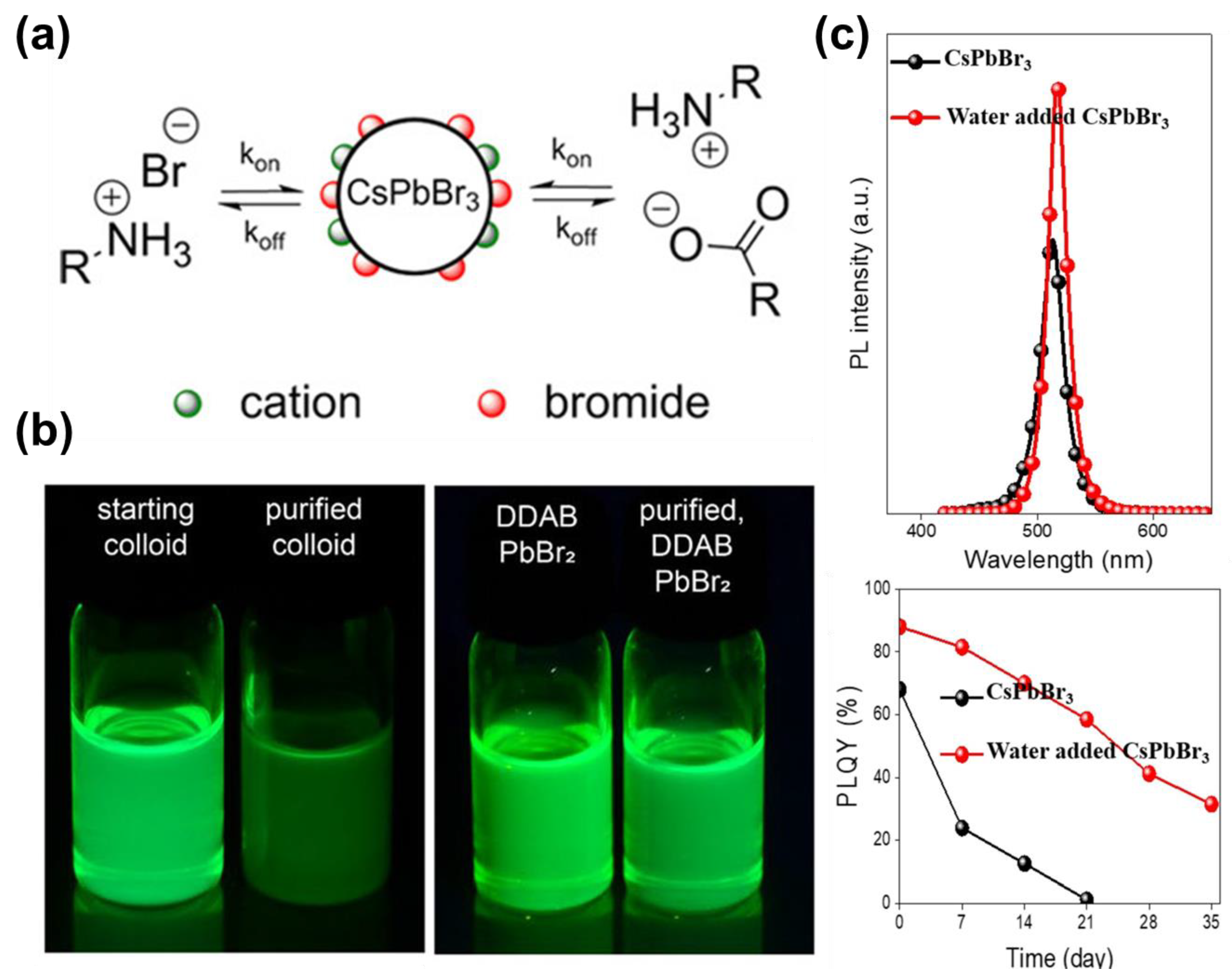
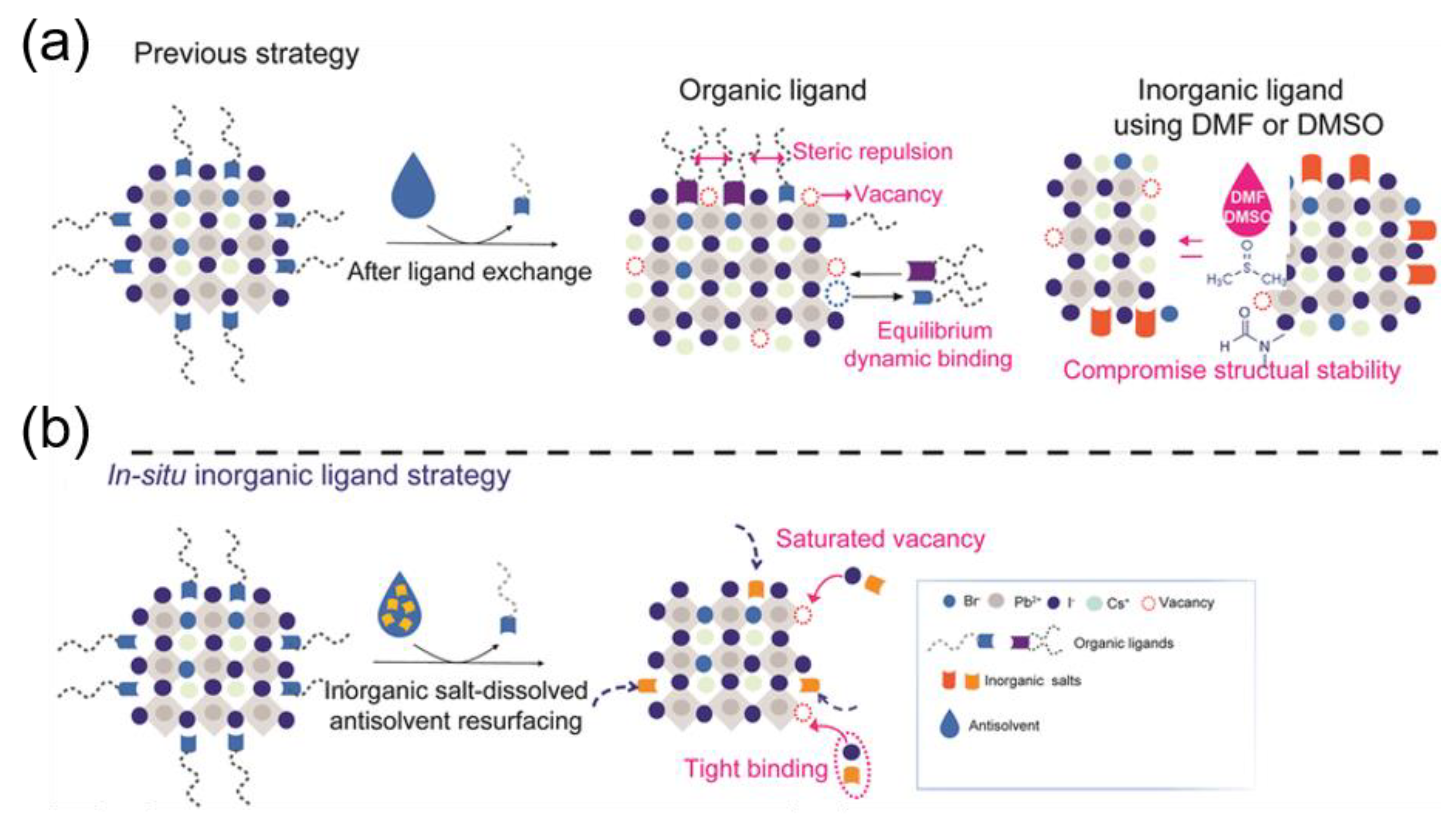
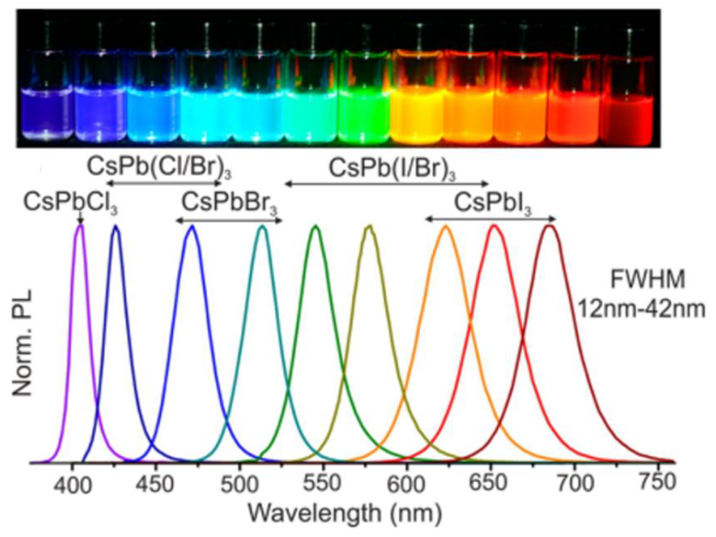
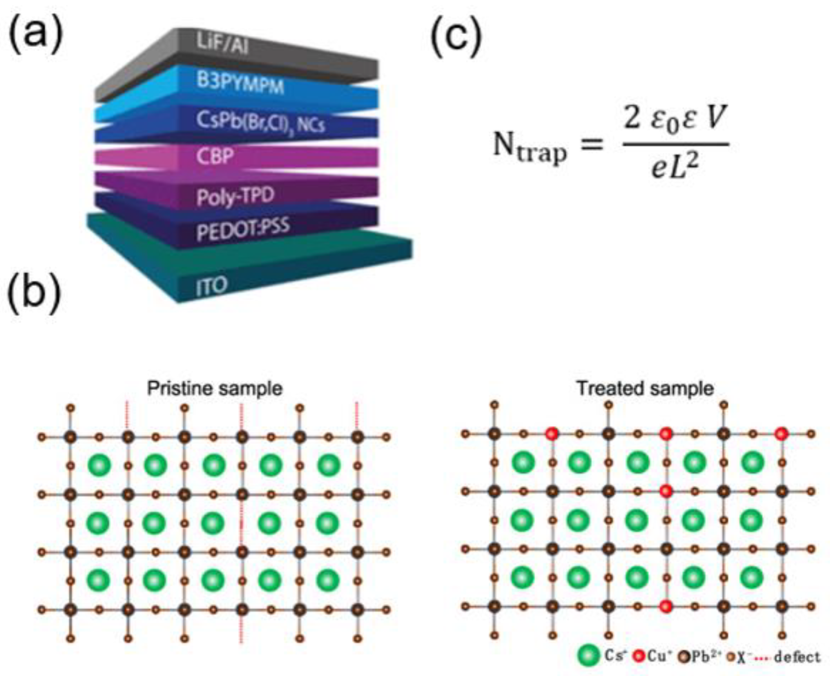
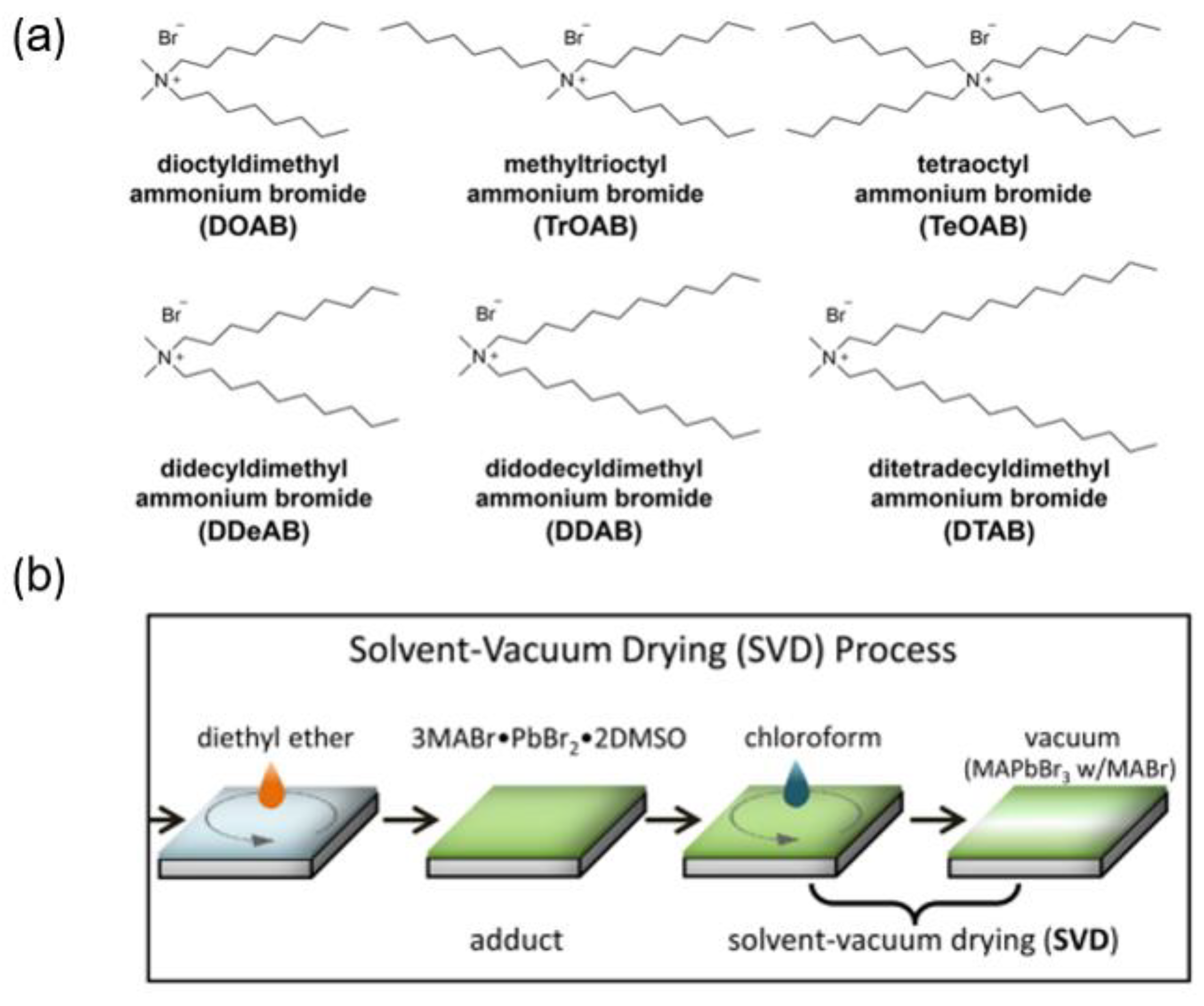
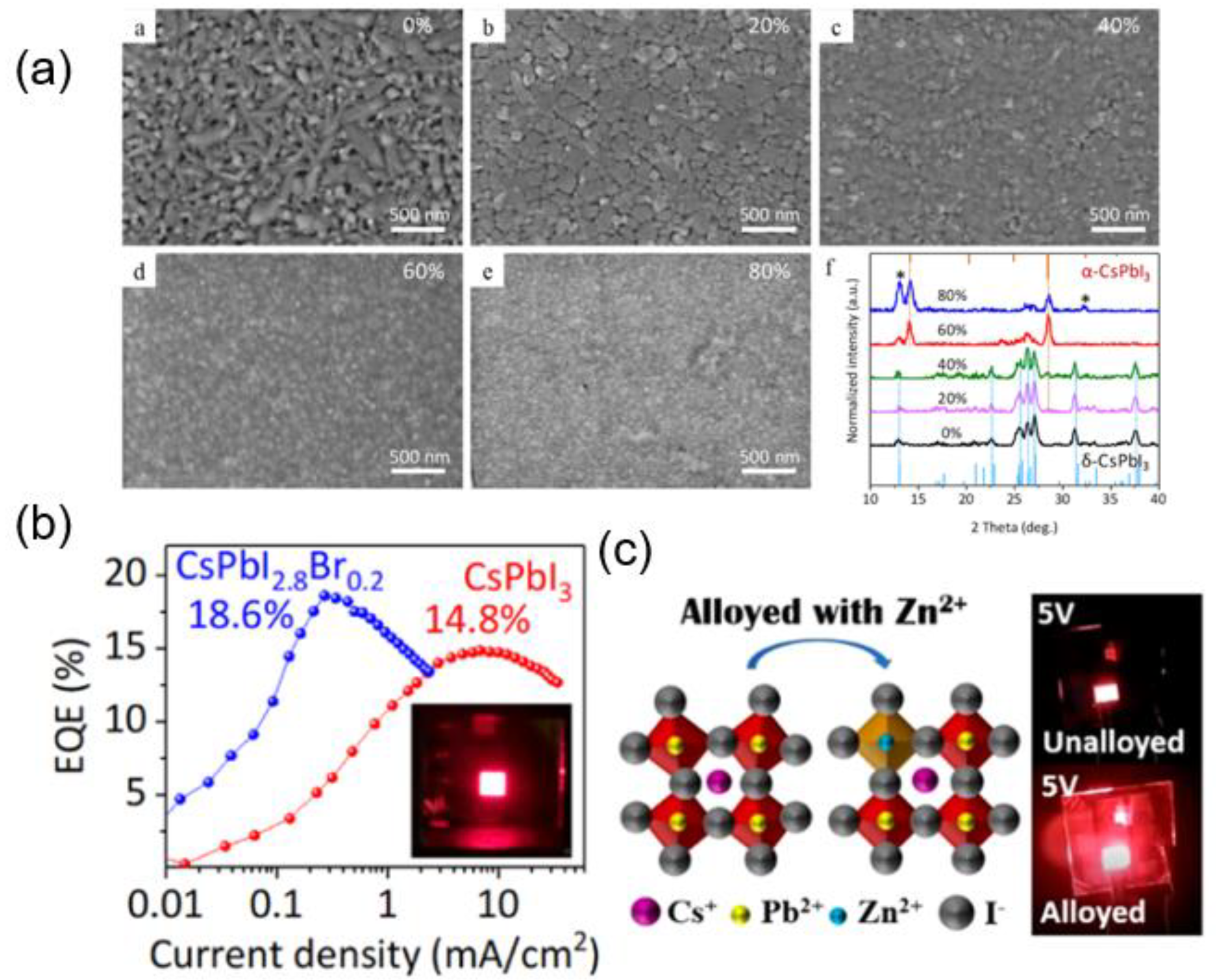
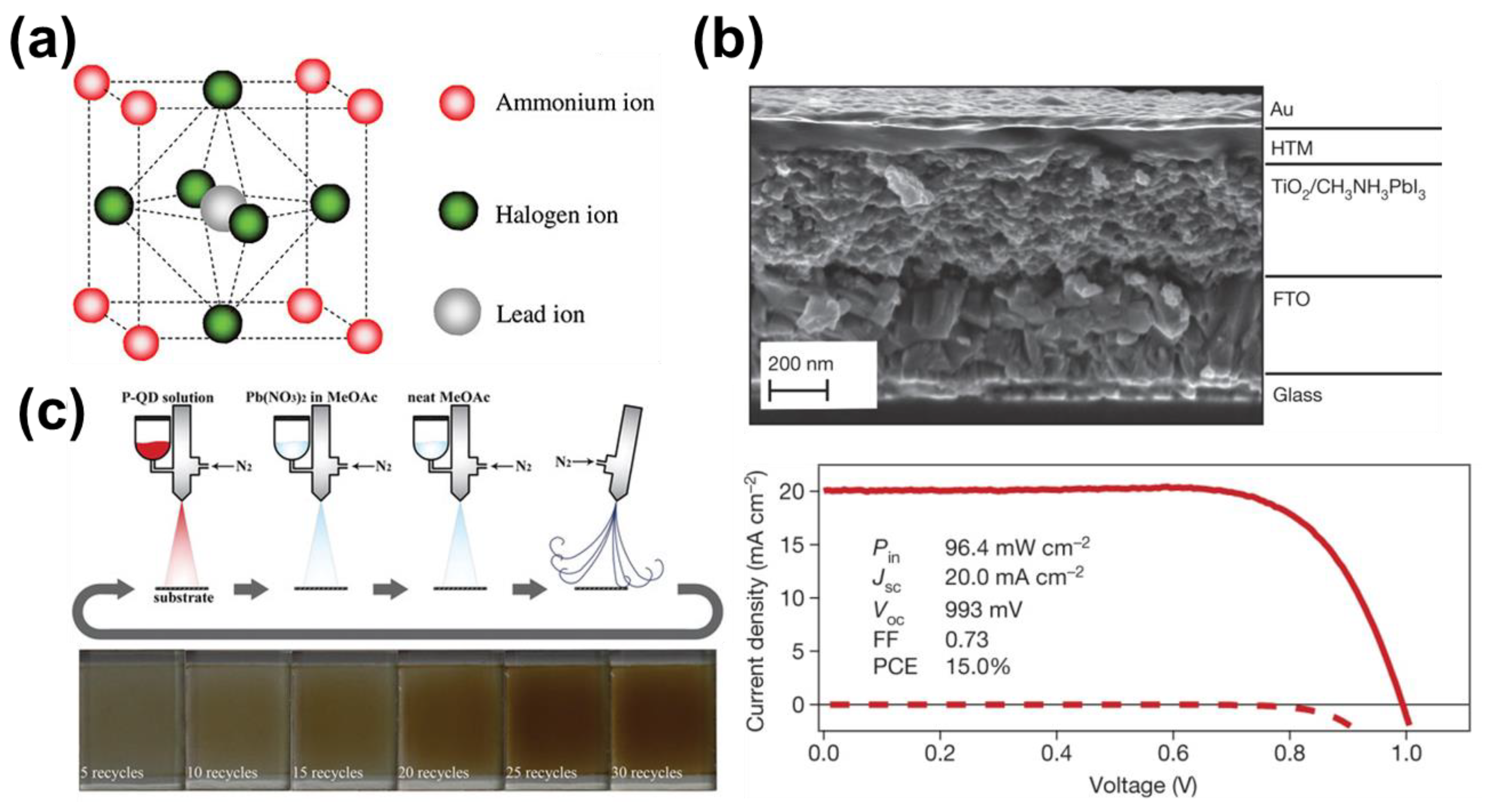
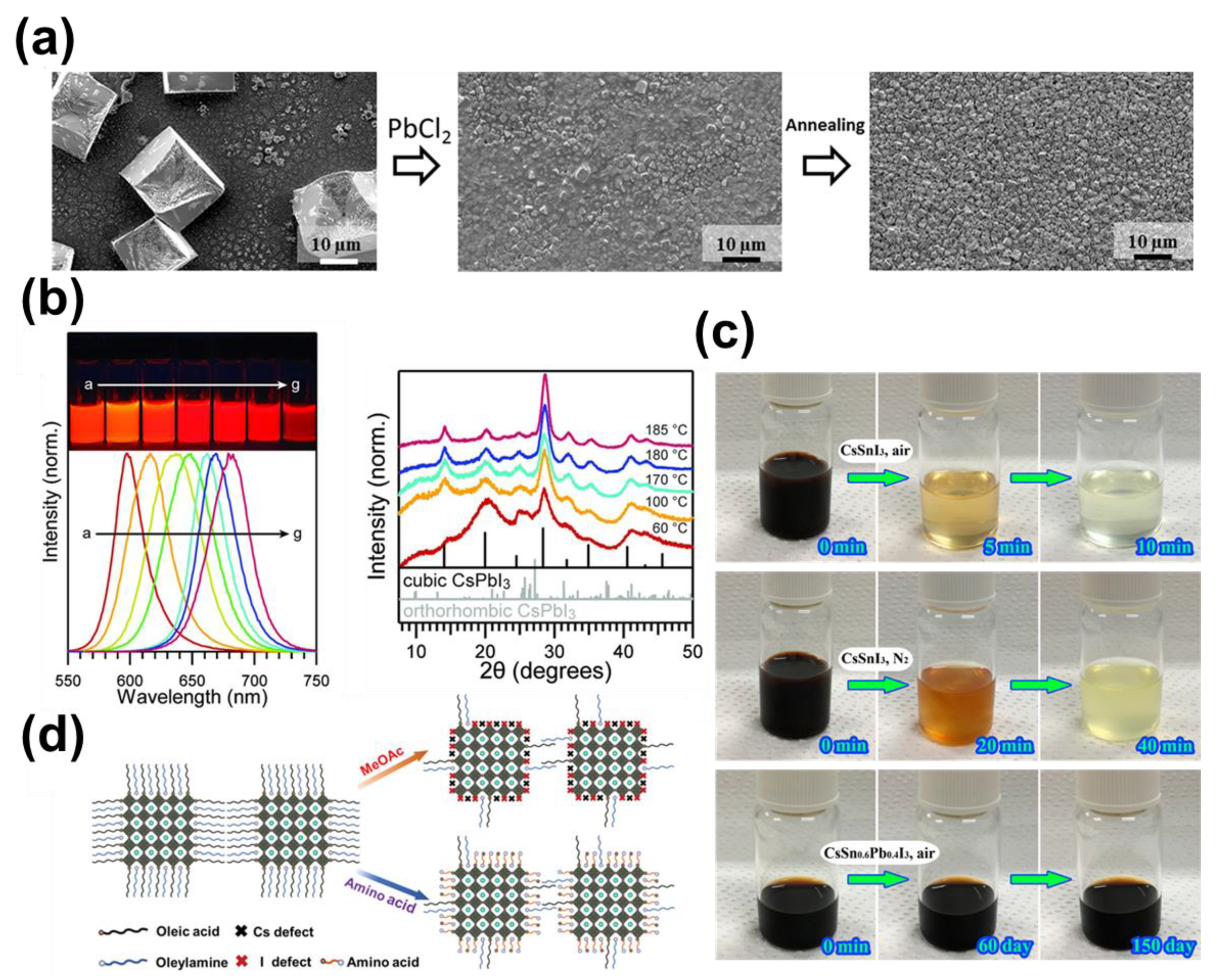
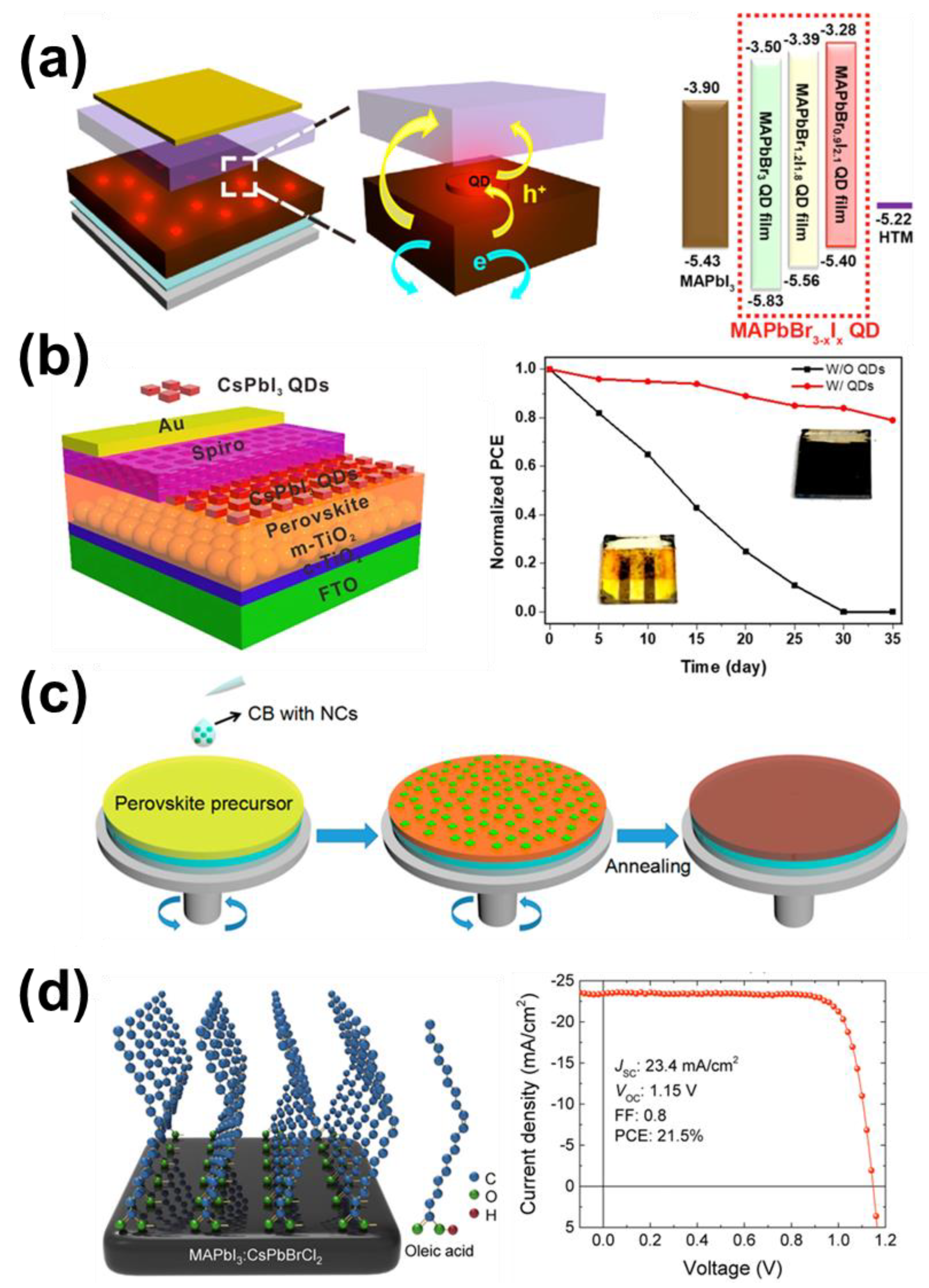
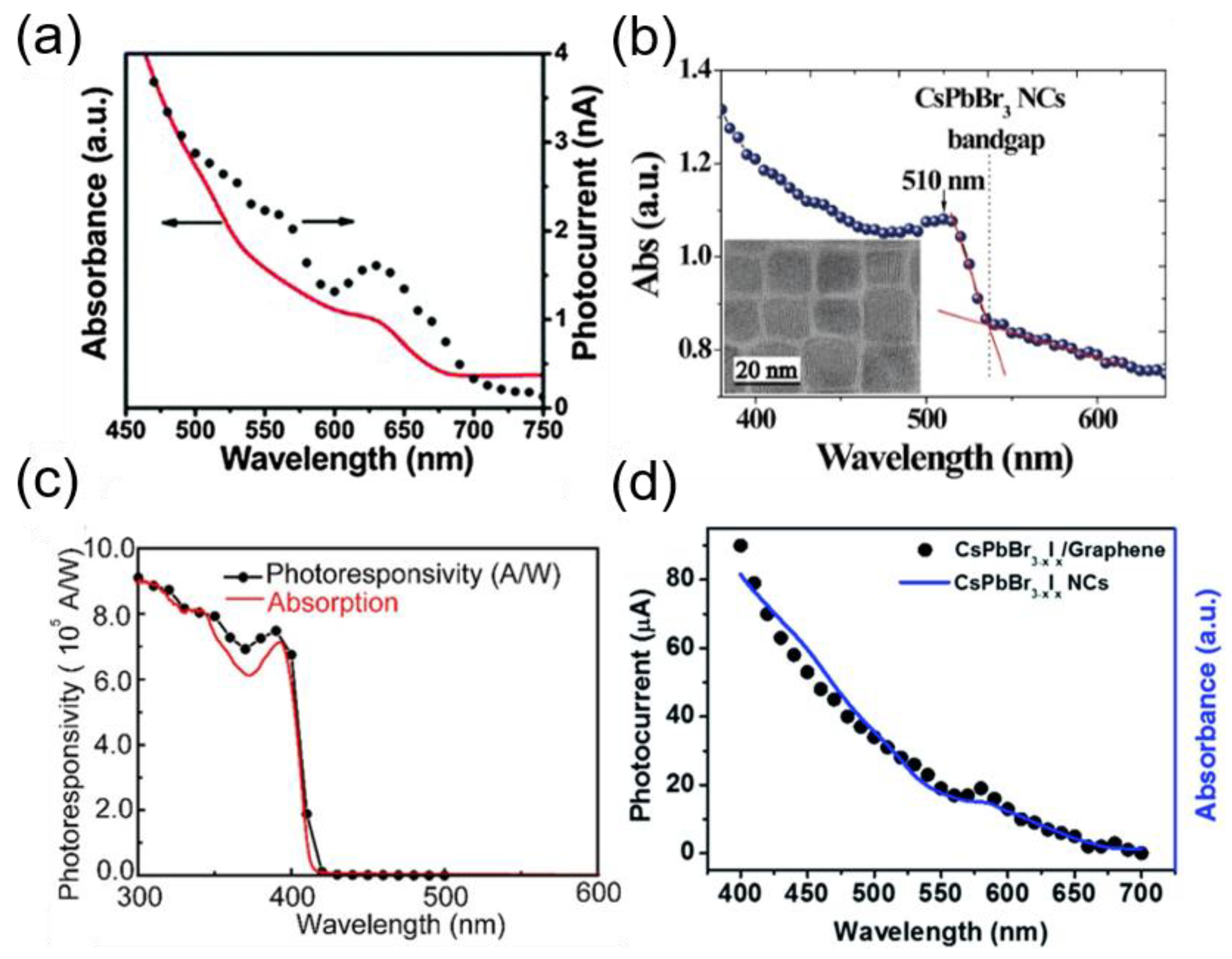
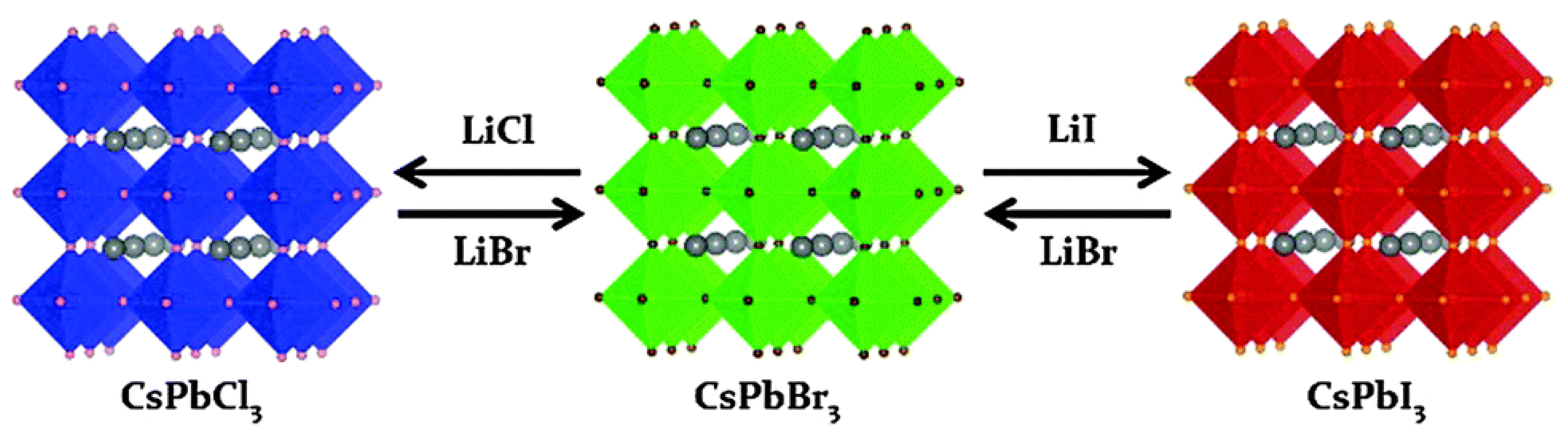
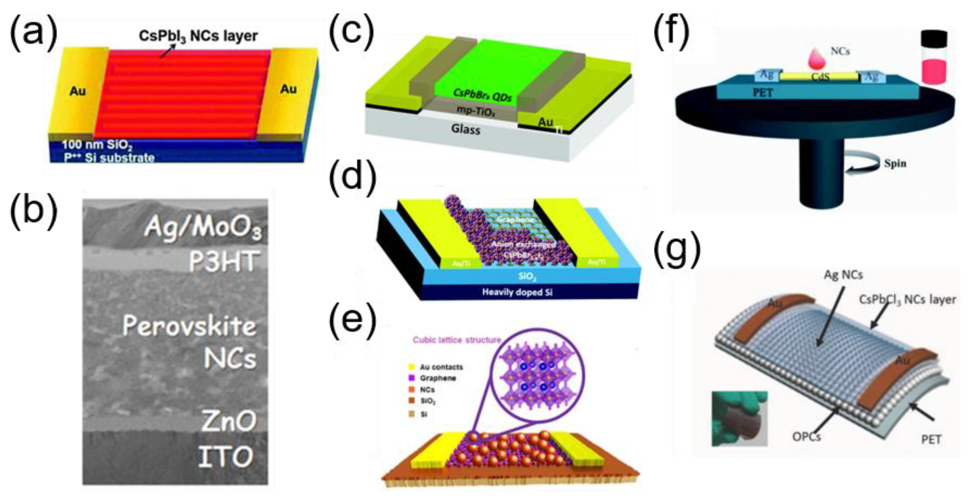
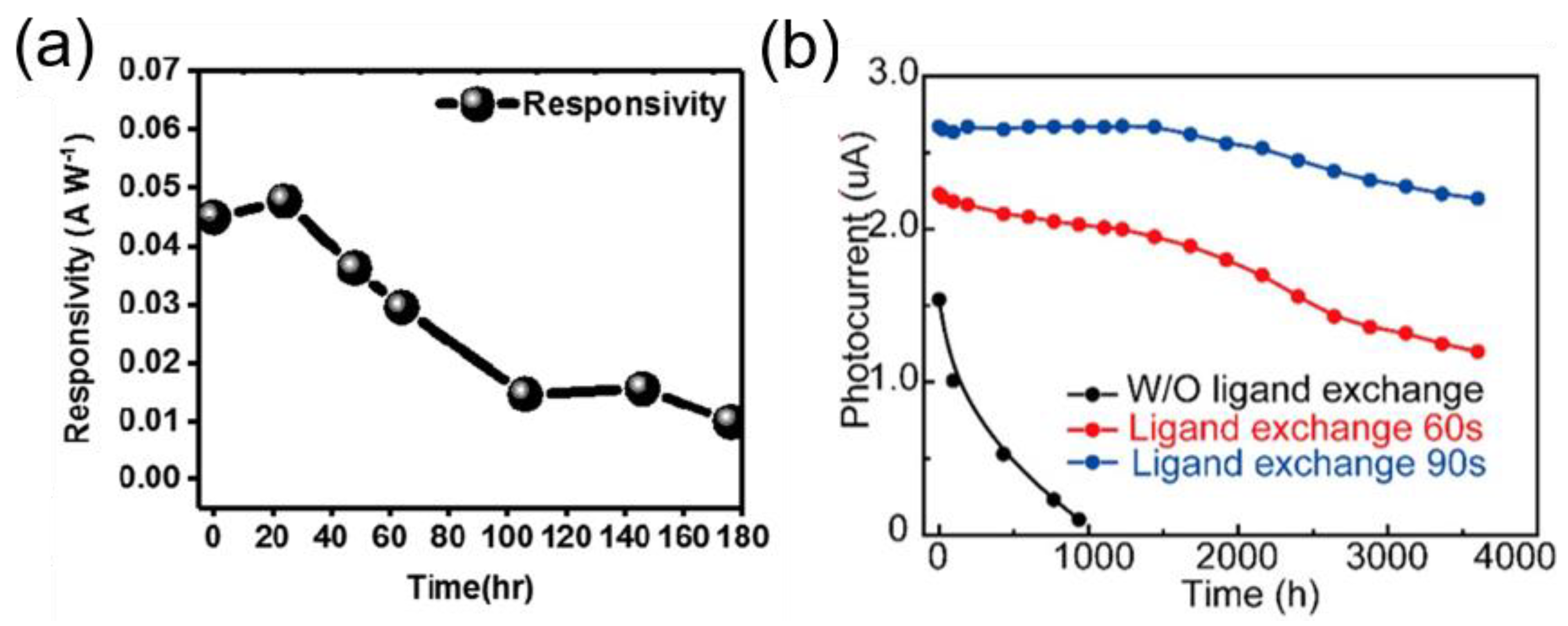
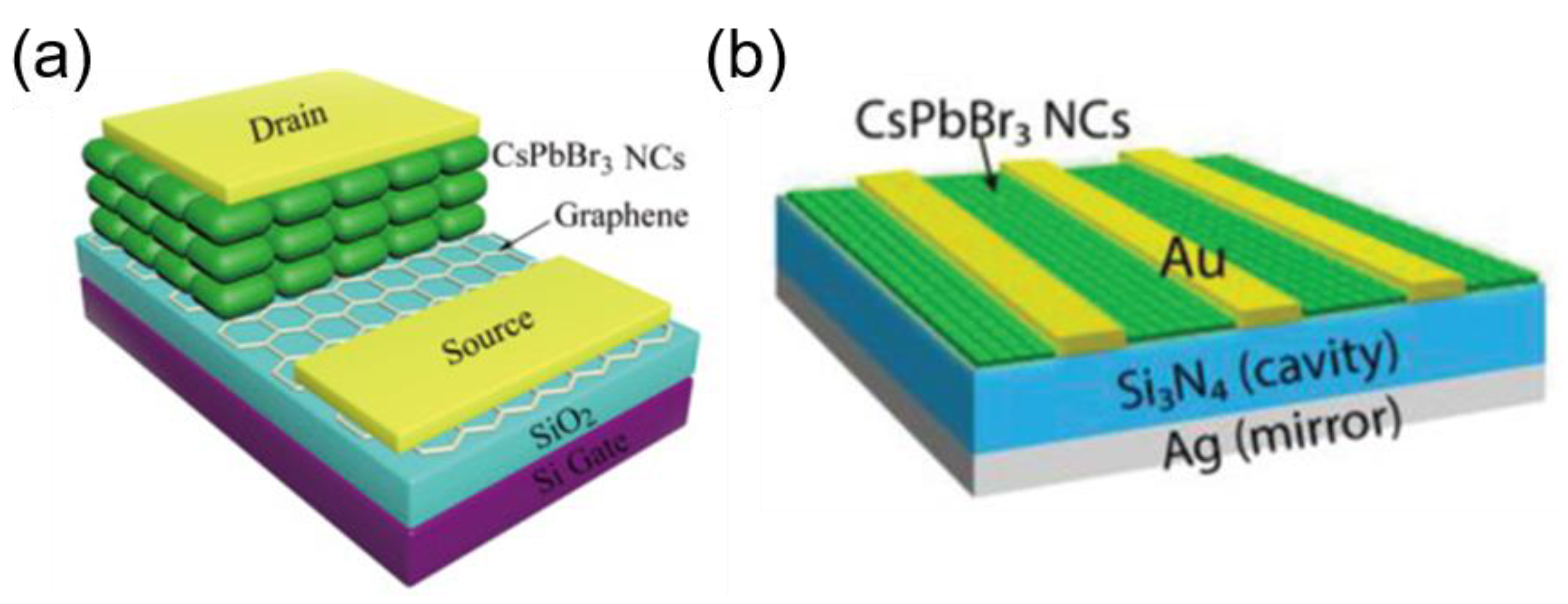
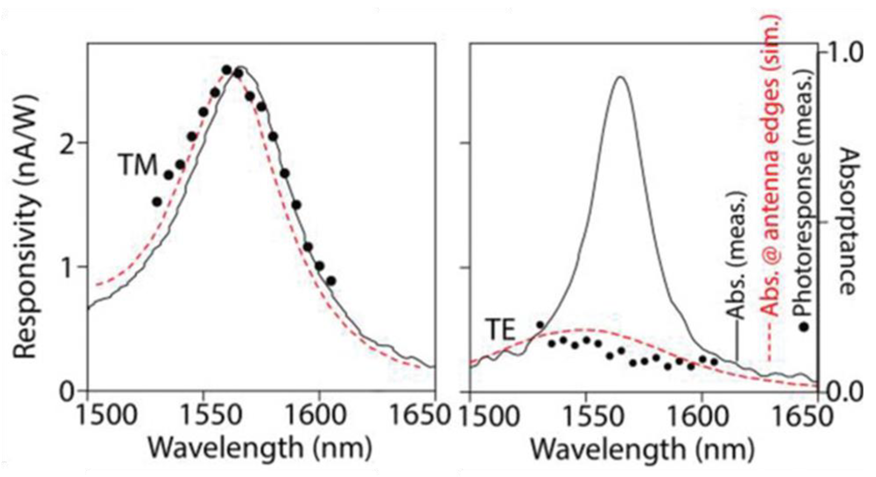
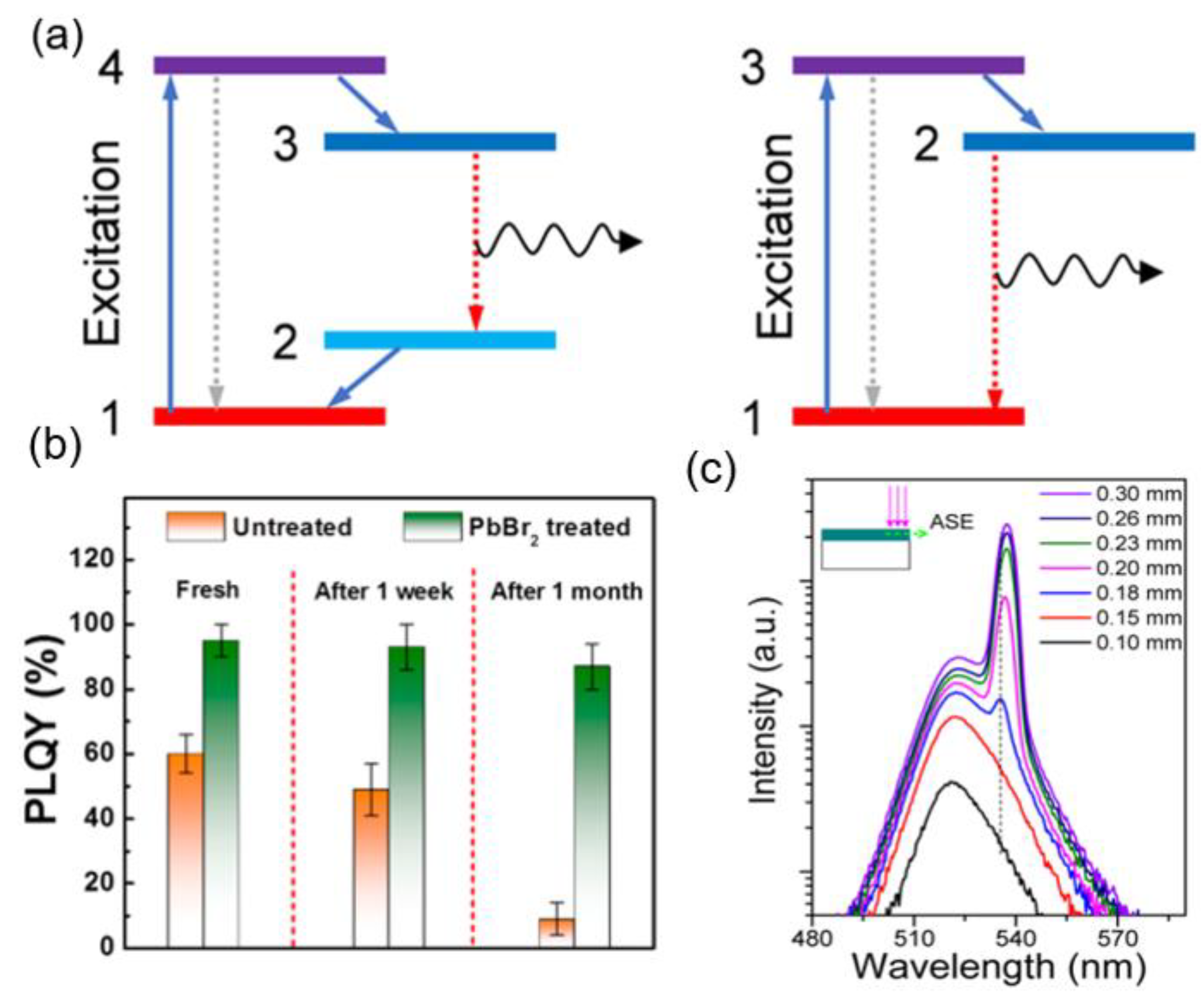
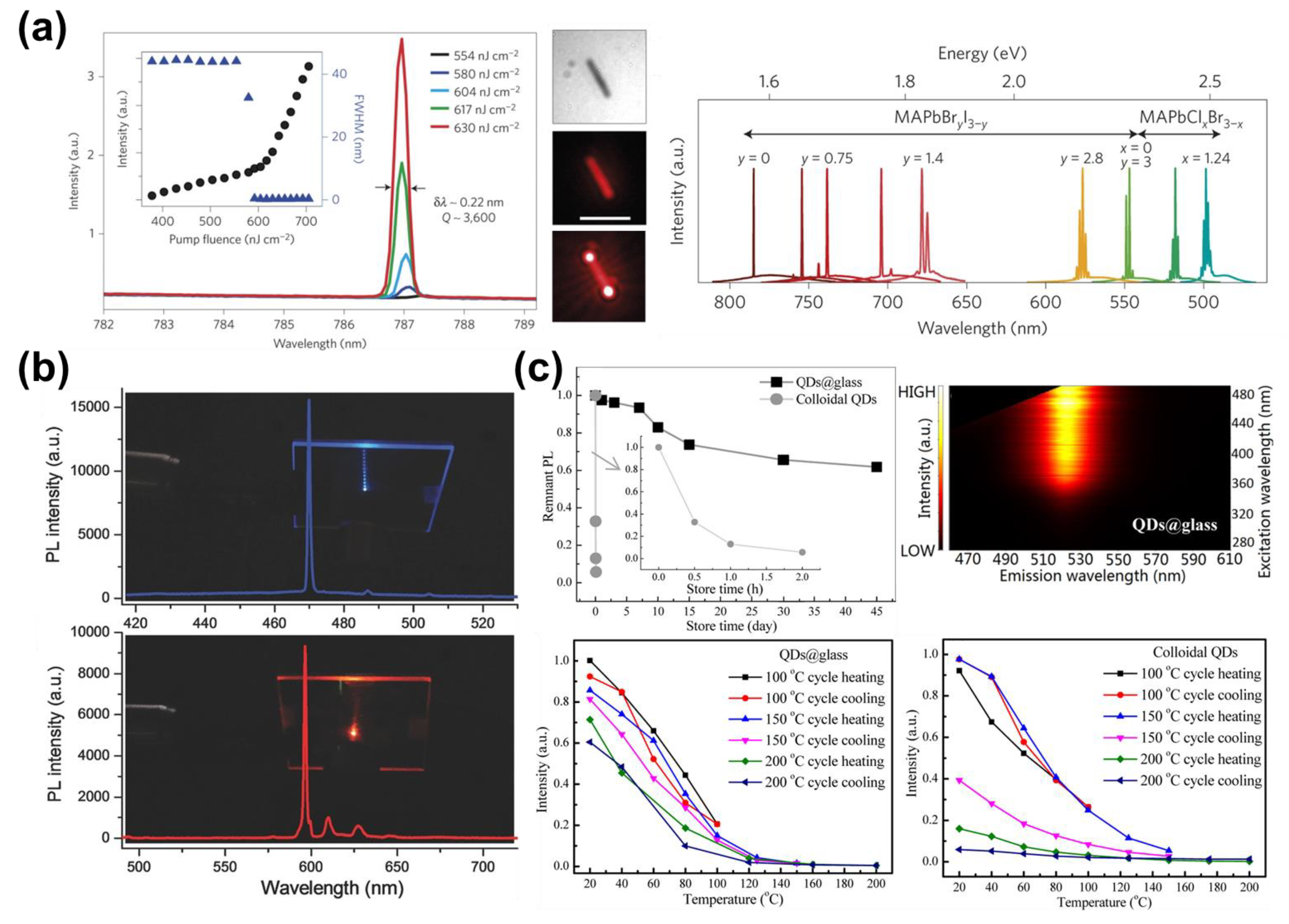
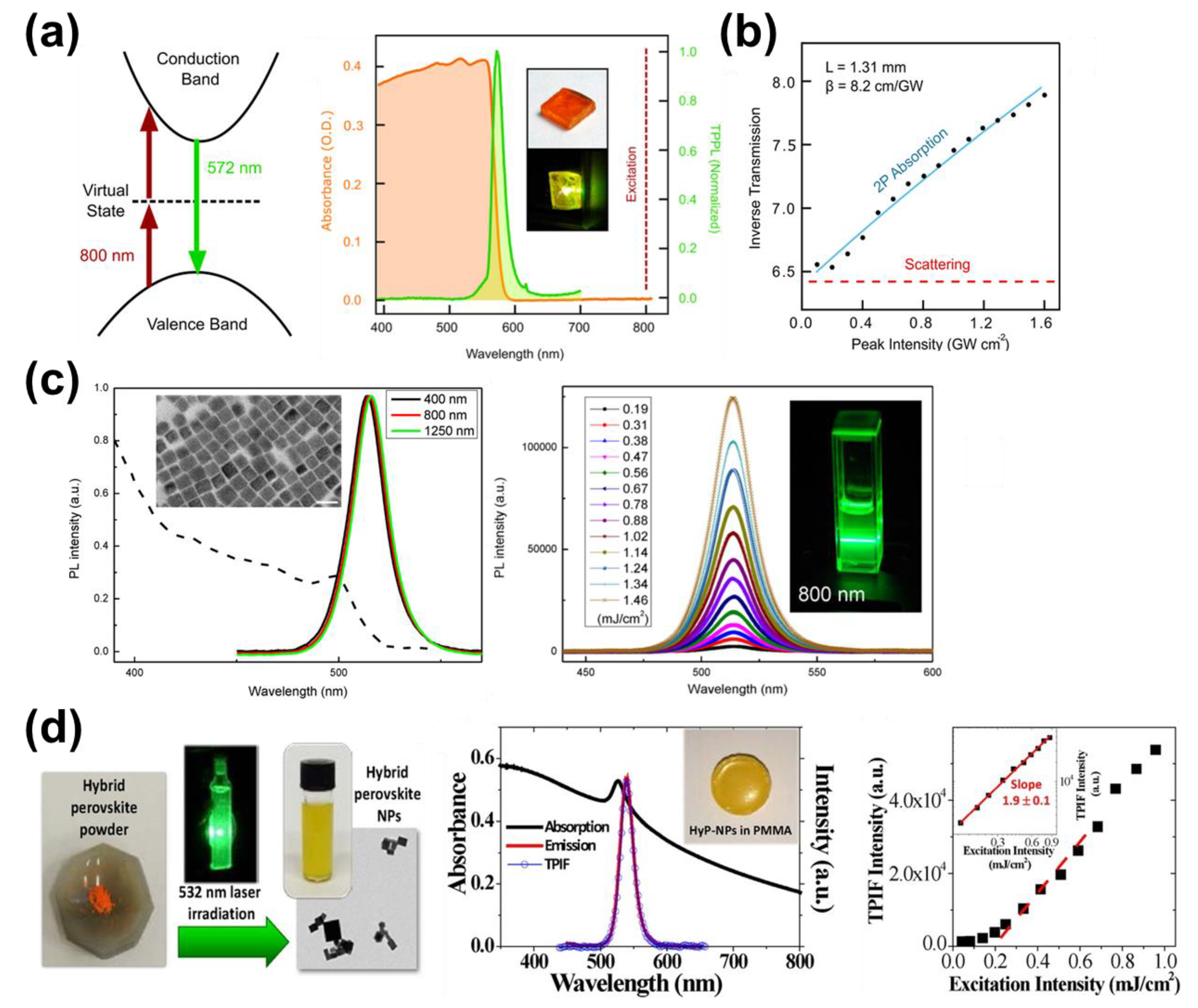
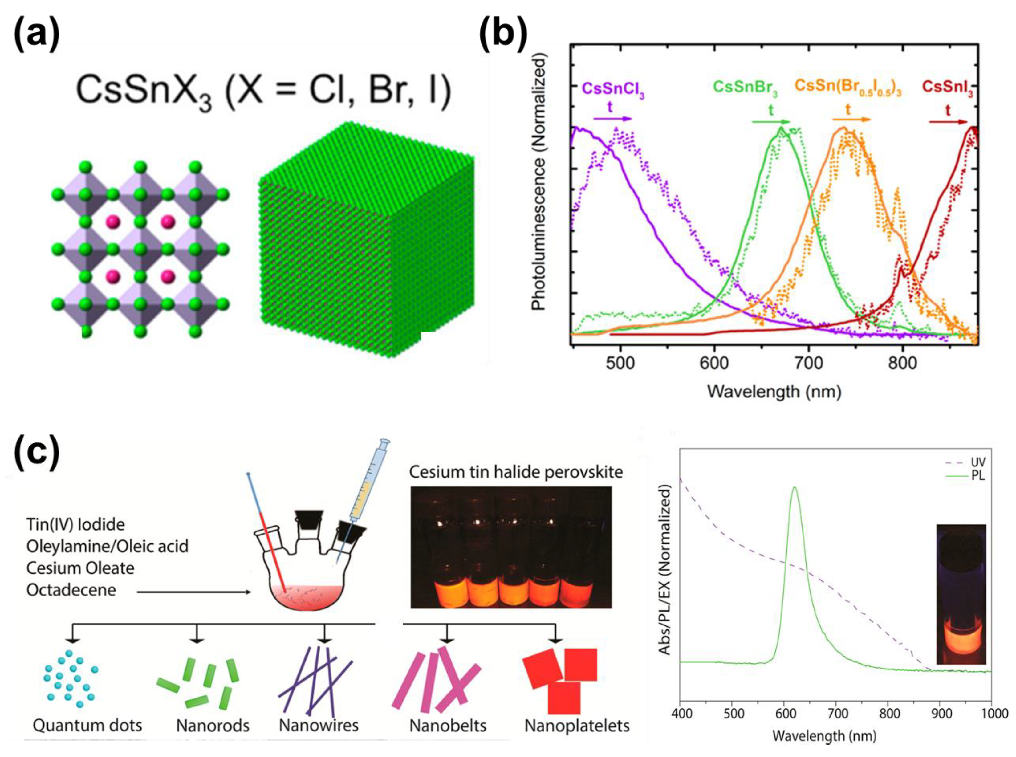
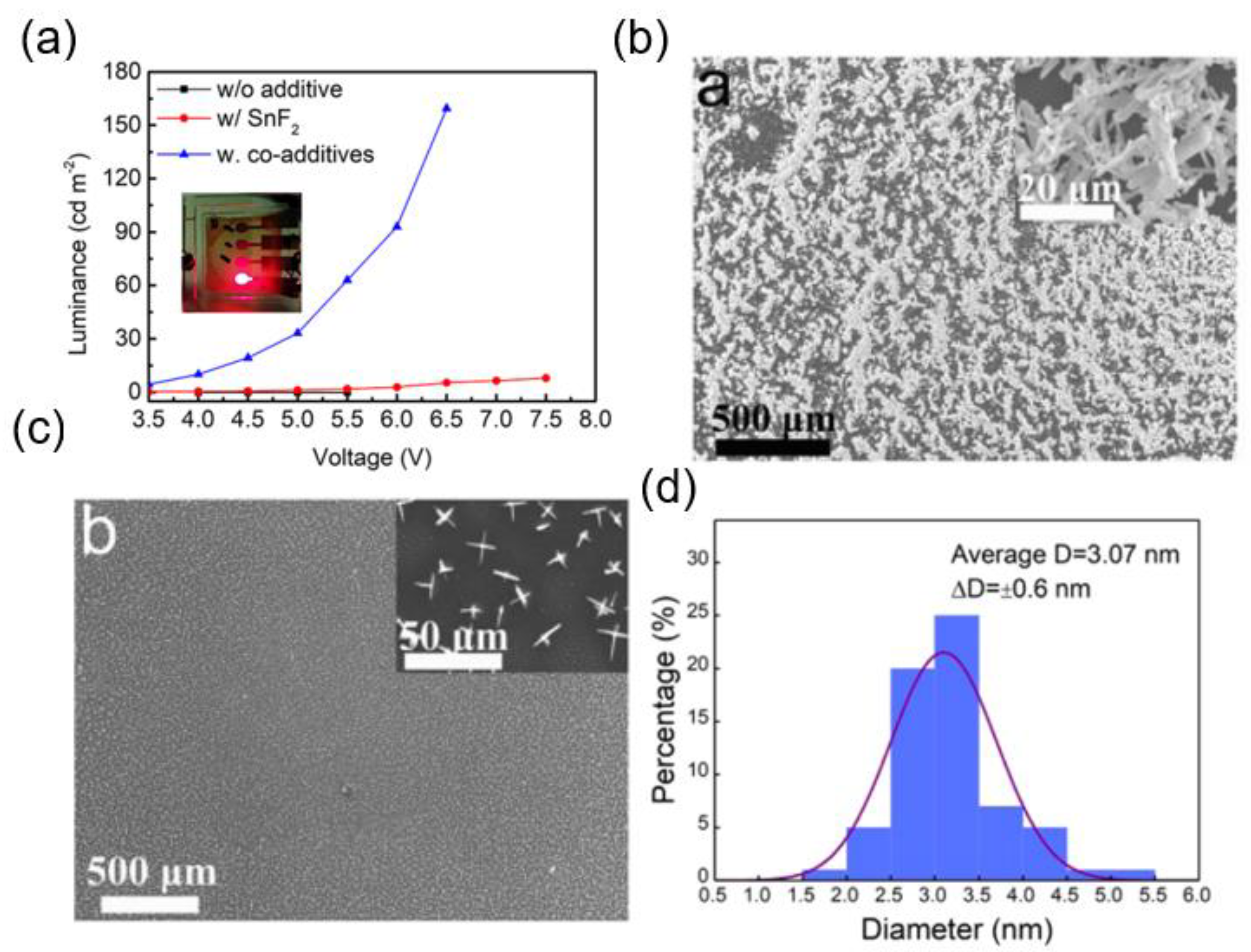
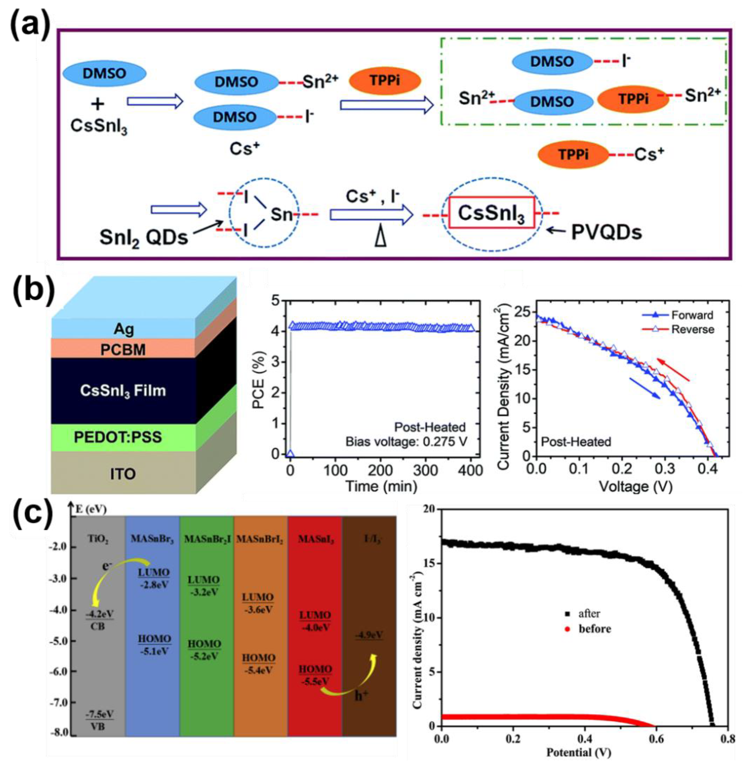
Table 1.
Result of perovskite film after ligand exchange. KI inorganic ligand increased the mobility from 9 × 10⁻⁴ cm2 V−1 s−1 to 6 × 10⁻² cm2 V−1 s−1 [14]. Hexyl amine ligand and octyl amine ligand can both increase hole mobility. The values of hole mobility are 6.2 × 10⁻³ cm2 V−1 s−1 and 1.3 × 10⁻³ cm2 V−1 s−1, respectively [15]. 2-aminoethanethiol (AET) enhanced electron mobility from 8.1 cm2 V−1 s−1 to 11.8 cm2 V−1 s−1 [16]. The aromatic acid/amine (benzoic acid or 4-phenylbutylamine) can shorten the distance between QDs and reduce leakage current [17]. Both DPPA (3,3-Diphenylpropylamine) + TCA (Trans-cinnamic acid) and DPPA + TFCA (derivates of trans-cinnamic acid) can make charge transport faster [18]. N/A means with no available data.
| Ref | Ligand | Result | Perovskite | PLQY (%) |
|---|---|---|---|---|
| [14] | KI inorganic ligand | The mobility increased | CsPb(IxBr1−x)3 NC | 95% |
| [15] | Hexyl amine ligand | Hole mobility increased | CH3NH3PbBr3 QDs | 82% |
| [15] | Octyl amine ligand | Hole mobility increased | CH3NH3PbBr3 QDs | 78% |
| [16] | 2-aminoethanethiol (AET) | Higher electron mobility | CsPbI3 QDs | 51% |
| [17] | aromatic acid/amine | Dense and uniform thin film | CsPbBr3 QDs | N/A |
| [18] | DPPA + TCA | faster charge transport time | MAPbBr3 QDs | 90% |
| [18] | DPPA + TFCA | faster charge transport time | MAPbBr3 QDs | 46% |
Table 2.
Component parameter arrangement in the blue and cyan light range.
| Ref | Perovskite | Modified | EL Peak | EQE (%) |
|---|---|---|---|---|
| [4] | CsPbClBr2 | Add Cu+ | 479 nm | 3.78% |
| [51] | CsPb(Br/Cl)3 | Adding Br and Cl in different ratios | 463 nm | 1.2% |
Table 3.
Component parameter arrangement in the green light range.
| Ref | Perovskite | Modified | EL Peak | EQE (%) |
|---|---|---|---|---|
| [3] | FAPbBr3 | Add DPPA-Br as a ligand | 528 nm | 16.3% |
| [38] | CsPbBr3 | Change ligand (QABs) | 513 nm | 9.71% |
| [52] | MAPbBr3 | Change ratio MABr and PbBr2 | 540 nm | 8.21% |
| [53] | MAPbBr3 | Two layers ETL | 525 nm | 12.9% |
Table 4.
Component parameter arrangement in the orange and red light range.
| Ref | Perovskite | Modified | EL Peak | EQE (%) |
|---|---|---|---|---|
| [5] | CsPb0.64Zn0.36I3 | Add Zn2+ | 668 nm | 15.1% |
| [56] | CsPbI3 | Add 4-F-PMAI | 692 nm | 14.8% |
| [57] | MAPbI3 | Add 4-F-PMAI | 749 nm | 7.9% |
Table 5.
Summary of rising time and decay time of hybrid graphene–perovskite NC photodetectors.
| Ref | Rise Time (s) | Decay Time (s) |
|---|---|---|
| [7] | 0.3 | 0.35 |
| [19] | 0.81 | 3.65 |
| [22] | 0.02 | 0.036 |
| [81] | 0.2736 | 2.26 |
Table 6.
Summary of PLQY and emission peaks for colloidal Cs3Sb2X9 IPQDs Copyright 2017, American Chemical Society.
Disclaimer/Publisher’s Note: The statements, opinions and data contained in all publications are solely those of the individual author(s) and contributor(s) and not of MDPI and/or the editor(s). MDPI and/or the editor(s) disclaim responsibility for any injury to people or property resulting from any ideas, methods, instructions or products referred to in the content. |
© 2023 by the authors. Licensee MDPI, Basel, Switzerland. This article is an open access article distributed under the terms and conditions of the Creative Commons Attribution (CC BY) license (https://creativecommons.org/licenses/by/4.0/).
Share and Cite
MDPI and ACS Style
Wang, Y.P.; Li, H.C.; Huang, Y.C.; Tan, C.S. Synthesis and Applications of Halide Perovskite Nanocrystals in Optoelectronics. Inorganics 2023, 11, 39. https://doi.org/10.3390/inorganics11010039
AMA Style
Wang YP, Li HC, Huang YC, Tan CS. Synthesis and Applications of Halide Perovskite Nanocrystals in Optoelectronics. Inorganics. 2023; 11(1):39. https://doi.org/10.3390/inorganics11010039
Chicago/Turabian StyleWang, Yen Po, Hsin Chieh Li, Yan Chi Huang, and Chih Shan Tan. 2023. "Synthesis and Applications of Halide Perovskite Nanocrystals in Optoelectronics" Inorganics 11, no. 1: 39. https://doi.org/10.3390/inorganics11010039
Note that from the first issue of 2016, this journal uses article numbers instead of page numbers. See further details here.