Abstract
Herein, we report the structural characterization and vibrational and physical properties of Cu2ZnSn1−xSixSe4 solid solutions synthesized using the ceramic method. X-ray diffraction analysis and Rietveld analysis of the samples indicated that by increasing the x value from 0 to 0.8, the volume of the unit cell decreased because the ionic radius of silicon is smaller than that of tin. Simultaneously, a phase transition between stannite and wurtz-stannite was observed. The Raman peaks were analyzed by fitting the spectra to identify the vibrational modes by comparison with the experimental data from Cu2ZnSnSe4 and Cu2ZnSiSe4. The spectra of Cu2Zn(Sn1−xSix)Se4 (x = 0.2 and 0.3) show two dominant peaks at approximately 172 and 195 cm−1, which are assigned to the A1 mode of the stannite structure. The optical band gaps for Cu2Zn(Sn0.8Si0.2)Se4 and Cu2Zn(Sn0.2Si0.8)Se4 were 1.30 and 1.74 eV, respectively. These values were intermediate to those of the end members. Electrical properties of Cu2Zn(Sn0.8Si0.2)Se4 revealed p-type conductivity behavior with a carrier concentration of approximately ~+3.50 × 10⁻¹⁹ cm−3 and electrical mobility of 2.64 cm2/V·s.
1. Introduction
In the face of the global energy crisis, research on CZTS-type semiconductor materials has grown in the last decade. These compounds are potential absorber materials for solar cells that use accessible materials with low toxicity, a suitable band gap (1.5 eV), and a high absorption coefficient (104 cm−1) [1,2]. Therefore, solid solutions of CZTS-type semiconductors are highly significant for photovoltaic applications [3,4].
CZTS-derivatives have been shown to exist in various phases such as kesterite (KS), stannite (ST), and wurtzite (WZ) [5,6,7]. The coexistence of the first two phases is possible because of the similar lattice parameters, bonding, and total energy of the kesterite and stannite tetragonal crystal structures. The wurtzite phase had a hexagonal crystal cell. The kesterite family includes Cu2ZnSnSe4 (CZTSe), Cu2ZnSn(S,Se)4 (CZTSSe), and Cu2ZnSnS4 (CZTS), and has a band gap between 1.0–1.5 eV that can be tuned by changing the [S]/[S + Se] ratio or realizing cationic substitution in the initial compound [3,8,9]. The ideal bandgap that the materials must possess for the optimal interconversion of energy and the application of solar cells has been established at approximately 1.5 eV.
The cationic substitution in the CZTS derivatives can generate evident changes in the electrical properties of the initial compound, but not in the structural changes, particularly when the powder X-ray technique is used. In this last case, Raman spectroscopy becomes a powerful tool to distinguish different crystal structures. This is because the spectrum is sensitive to the local atomic environment, the strength of chemical bonds, masses, and charges of the constituent elements. This allows similar structures to be distinguished from one another. For example, three dominant peaks characterize the spectra of wurtz-stannite crystals, whereas stannite or kesterite crystalline structures present two dominant peaks [10,11,12]. In terms of electrical properties, cationic substitution can change the electrical behavior because it modifies the electrical mobility, and the carrier concentration and conductivity are important parameters for solar cell performance. In-CZTSe exhibited p-type electrical conductivity with a conductivity of 11.7 S·cm−1 and a mobility of approximately 8.0 cm2·V−1·s−1 [13]; whereas, the Mg-doped CZTSe showed n-type behavior with an electrical conductivity and mobility of 24.6 S·cm−1 and 120 cm2·V−1·s−1, respectively [14], and both materials were found to be attractive as absorber layer materials.
The Si substitution of Sn in CZTS has attracted significant interest for its potential applications because Si exhibits important semiconductor properties, and this type of compound is a p-type semiconductor. The band gap in CZTSe-derivative, where tin has been completely replaced by silicon, has demonstrated experimental values of 2.71 eV [15] for Cu2ZnSiS4 and 2.33 eV [16] for Cu2ZnSiSe4. However, when a partial substitution of tin for silicon occurs, a band gap of 1.7 eV is obtained, which is close to the optimal values for a solar cell [4]. Another substitution is the Al substitution of Sn in CZTSe to form Cu-deficient Cu1.75Zn(Sn1−xAlx)Se4 where a decrease in the lattice constants a and c occurs with an increase in Al content because aluminum is much smaller than tin, which provides an approach for enhancing carrier mobility. The enhanced mobility can reduce carrier recombination and is important for further improving solar-cell efficiency. When x = 0.4 in Al-CZTSe manifests an electrical conductivity of 57.2 S·cm−1 with a hole mobility of 32.5 cm2/V·s [17]. Conversely, the Ge-substitution of Sn in CZTS can lead to a tunable band gap, in this case, from 1.4 to 2.2 eV by adjusting the Ge/Sn ratio. Increasing the amount of Ge causes a decrease in the lattice parameters, which can be explained by the replacement of Sn atoms by small Ge atoms, which can be followed by X-ray Powder Diffraction (PXRD) and Raman changes [9,18,19,20].
Herein, the structural characterization, as well as the effect on spectroscopic, optical, and conductivity properties of compounds derived from Cu2ZnSnSe4 (CZTSe), where tin is partially substituted by silicon to form Cu2Zn(Sn1−xSix)Se4, were explored. The compound Cu2ZnSnSe4 adopts a tetragonal stannite structure, whereas Cu2ZnSiSe4 crystallizes in the wurtz-stannite structure. Considering that the two end members of the Cu2Zn(Sn1−xSix)Se4 series crystallize in different structural arrangements, a transition can be expected at a given substitution value, similar to the CZTS sulfur phase. Vibrational analysis showed that the A1 modes in the stannite structure () and A1 and B1 modes in wurtz-stannite () were Raman-active. The signals were compared excellently with the Raman spectra of the end members. Rietveld analyses, XRD patterns, backscattered images, and energy-dispersive X-ray spectroscopy (EDS) revealed that the samples were homogenous within the detection limits for x = 0.2 and 0.3 in Cu2Zn(Sn1−xSix)Se4. The electrical measurements suggested p-type semiconductor behavior.
2. Materials and Methods
2.1. Synthesis
Polycrystalline Cu2ZnSn1−xSixSe4 compounds were prepared by directly combining high-purity elemental powders (99.99%, purity, Sigma-Aldrich, St. Louis, MO, USA) in stoichiometric amounts. All manipulations were performed under an argon atmosphere. The reaction mixtures were sealed in evacuated quartz ampoules and placed in a programmable furnace. The ampoules then were gradually heated to 900 °C at 150 °C/h, maintained at this temperature for ~72 h, and slowly cooled from 900 °C to room temperature at a rate of 25 °C/min.
2.2. Powder X-ray Diffraction Measurements
Powder X-ray diffraction (PXRD) patterns were collected at room temperature using a Bruker D8 Advance diffractometer (Bruker, Billerica, MA, USA) equipped with a Cu Kα radiation source in the range of 5° < 2θ < 80°.
2.3. SEM-EDS Analysis
The chemical compositions were determined by energy-dispersive X-ray analysis using a Bruker Vega 3 Tescan system equipped with a Quantax 400 (EDS, Oxford LinK ISIS microanalyzer, Oxford Instruments, Abingdon, UK)) microanalyzer (SEM, JEOL 5400 system, Tokyo, Japan). The samples were mounted onto a double-sided carbon tape, which was adhered to an aluminum specimen holder.
2.4. Raman Scattering Measurements
Raman scattering measurements were performed using an RM1000 Renishaw micro-Raman spectrometer with CCD detectors in combination with a Leica LM/PM microscope using 514 nm wavelength excitation. The spectrometer was calibrated using a reference single-crystal Si sample (Raman peak at 520.7 cm−1). Spectral data were collected at room temperature in the backscattering configuration in the spectral range of 100–500 cm−1 with a laser spot on a sample of approximately 1 μm and a laser power of 2 mW.
2.5. Diffuse Reflectance Measurements
Diffuse reflectance spectra were recorded on a Sciencetech, NIR spectrophotometer. The measurements were carried out between 300 and 1800 nm using the Acquisition software SciSpec 10.0.1.0, Analysis software SciAnalysis 1.1.2.0, FGS-20-01c: Grey Fluorilon (Diffuse Reflectance 20%) as a Standard Reference, Si (180–1100 nm) detector.
2.6. Electrical Properties
Hall-effect measurements were performed using ECOPIA HMS 2000 (ECOPIA, Anyang-city, Gyeonggi-do, South Korea) equipment. The pellets for the electrical measurements were uniaxially pressed at ~2.5 tons, resulting in cylindrical pellets with a 9.00 mm diameter and thickness of 0.93 mm. The Hall coefficient, ±0.556 T, was obtained from a linear fit of the Hall resistivity.
3. Results and Discussion
3.1. X-ray Powder Diffraction and Compositional Characterization
The PXRD patterns of polycrystalline Cu2ZnSn1−xSixSe4 (x = 0.2, 0.3, 0.5, 0.7, and 0.8) are shown in Figure 1. These phases were fully indexed in the stannite group I and wurtz-stannite or Enargite group and the patterns were refined by the Rietveld method (Figure 2).
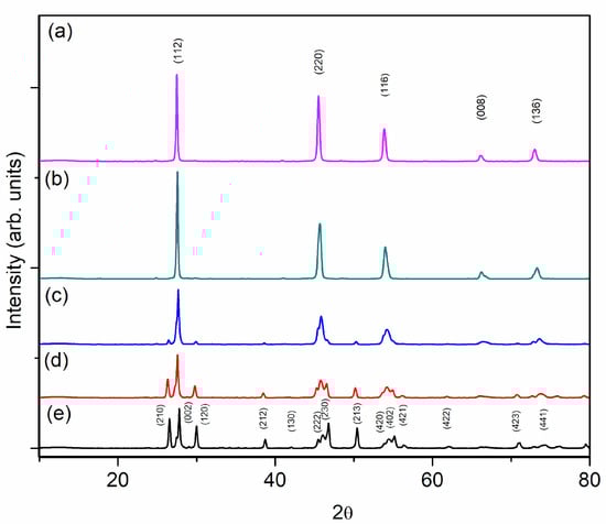
Figure 1.
X-ray powder diffraction patterns for Cu2ZnSn1−xSixSe4, 0.2 ≤ x ≤ 0.8 (a–e).
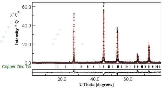
Figure 2.
An example of Rietveld Refinement of the XRD data obtained for Cu2ZnSn0.8Si0.2Se4, which was performed with the MAUD software (version 2018). Bragg’s R-factors were Rb = 8.804 and Rwp = 13.754.
The final structural parameters are summarized in Table 1. Samples with a lower amount of Sn present a higher indexing percentage in the wurtz-stannite group [21], and as the Sn percentage increases, a higher indexing is achieved in stannite but still with signals belonging to the group.

Table 1.
Rietveld refinement of cell parameters for Cu2ZnSn1−xSixSe4.
As shown in Table 1, as the amount of silicon increases, the volume of the unit cell decreases because the ionic radius of silicon (0.26 Å) is smaller than that of tin (0.55 Å) [22]. In addition, it is observed that there is a phase transition in the samples with a greater amount of Sn; they have a stannite-type structure, and when the Si content increases, they pass to a wurtzite-type structure. For x = 0.5, two phases were detected (tetragonal and orthorhombic) with cell parameters that remained almost constant. Table 1 lists the cell parameters of the major components. The samples were single-phase, with x < 0.3. In all other samples, two phases coexist: the tetragonal stannite structure () and orthorhombic wurtz-stannite (). The evolution of the unit cell volume for x = 0.2, 0.3, and 0.5 follows Vegard’s law, which demonstrates that the members of the Si-poor content belong to distinguishable solid solutions.
The chemical compositions of the powder samples were determined by EDS analysis of the surfaces of the sample pellets. The backscattered images and EDS analysis (chemical maps of several areas) revealed that the samples were uniform throughout the scanned region (Figure S1). The experimental results reveal that the ratio Cu/Zn/Sn/Si/Se is 2.12/1.05/0.18/0.75/3.91, for example, to Cu2ZnSn0.2Si0.8Se4 nominal composition, as shown in Figure 3.
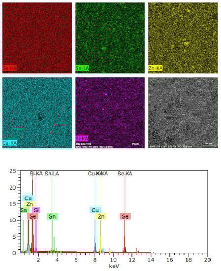
Figure 3.
Scanning electron microscopy analysis: Representative energy-dispersive X-ray spectroscopy mapping spectral analysis (powder sample) and backscattering electron image of Cu2ZnSn0.2Si0.8Se4.
All the nominal compositions of the samples are presented in Table 2.
Table 2.
Chemical composition of the samples Cu2ZnSn1−xSixSe4.
3.2. Raman Analysis and Diffuse Reflectance Measurements
We measured the Raman spectra of polycrystalline samples of the compounds Cu2Zn(Sn1−xSix)Se4 (x = 0.2, 0.3, 0.7, and 0.8), which present a phase transition from the stannite structure () to the structure type wurtz-stannite (), by replacing Sn atoms with silicon, which indicates a dependence on the chemical composition.
It has been reported that Cu2ZnSnQ4 (Q = S, Se) quaternary phases crystallize in the tetragonal stannite structure. In this structure, only Cu atoms form one plane; whereas, the next plane consists of Zn and Sn atoms. In contrast, the Cu2ZnSiQ4 (Q = S, Se) quaternary phases crystallized in an orthorhombic structure called wurtzite, where the layers formed by Zn and Si are separated by layers of Cu atoms. The Raman spectra of wurtz-stannite are characterized by three dominant signals, which contrasts with the spectra reported for similar quaternary compounds that crystallize in a stannite-like structure where two dominant signals of the A1 vibrational mode are observed [11].
Figure 4 shows the spectra measured for Cu2Zn(Sn1−xSix)Se4 compounds with x = 0.2 and 0.3. In them, it is possible to observe 7 signals, characterized by the presence of two dominant peaks at approximately 172 and 195 cm−1, which were assigned to the A1 mode of the stannite structure. The adjustment of the spectrum through Lorentzian curves has allowed the identification of the weakest vibrational modes and the frequencies of these peaks (see Table 3), which agrees with the values reported by Gürel et al. [23] and Fontané et al. [24] for quaternary compounds CZTSe (S).
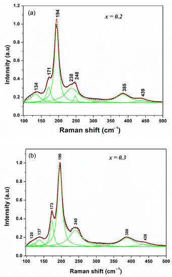
Figure 4.
Raman spectrum of Cu2Zn(Sn0.8Si0.2)Se4 (x = 0.2) (a) and Cu2Zn(Sn0.7Si0.3)Se4 (x = 0.3) (b) samples with stannite structure. Contribution of the different peaks deduced from the fit with Lorentzian curves (green lines).
Table 3.
Frequency and proposed mode assignment of Raman peaks from solid solutions Cu2Zn(Sn1−xSix)Se4 (x = 0.2, 0.3) and Cu2ZnSnSe4.
For its part, Figure 5 shows the Raman spectra of the Cu2Zn(Sn1−xSix)Se4 compounds for x = 0.7 and 0.8. By adjusting the Lorentzian curves, six signals were identified, of which three were assigned to the tetragonal crystal structure and the rest to the orthorhombic crystal structure. The spectra were dominated by a wide and intense split signal at ~200 cm−1 which was attributed to three bands centered at wavenumbers of ~219, 204, and 187 cm−1. Detailed analysis of this signal and considering the data obtained from the Rietveld refinement for these phases allows us to suggest that the peak at 218 cm−1 (x = 0.7) and 219 cm−1 (x = 0.8) of the spectra is attributed to the A1 vibration mode of the wurzt-stannite structure; simultaneously, in both spectra, a harmonic overtone of the A1 mode is observed at ~412 cm−1, a broad and weak peak, approximately twice the peak at ~219 cm−1, showed good agreement with the results reported by Levcenco et al. [25] and Guc et al. [11] for the quaternary compound CZSiSe.
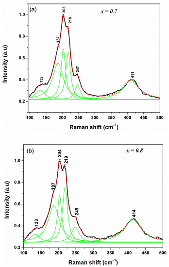
Figure 5.
Raman spectrum of Cu2Zn(Sn0.3Si0.7)Se4 (x = 0.7) (a) and Cu2Zn(Sn0.2Si0.8)Se4 (x = 0.8) (b) samples with wurtz-stannite structure. Contribution of the different peaks deduced from the fit with Lorentzian curves (green lines).
In contrast, the bands observed at 187 and 204 cm−1, which contribute to the dominant signal of both spectra (see Figure 5), are assigned to the A1 dominant mode of the stannite structure, demonstrating an excellent relationship with the peaks observed at ~172 and 195 cm−1 of the compositions x = 0.2 and 0.3 for our compound (Cu2Zn(Sn1−xSix)Se4, see Figure 4). This reveals the results of the Rietveld refinement for Cu2Zn(Sn0.3Si0.7)Se4 and Cu2Zn(Sn0.2Si0.8)Se4, which determines the mixture between the tetragonal () and orthorhombic () crystal structures.
The bands of the weakest contributions at ~132 and 248 cm−1 (see Figure 5) were assigned to the A1 symmetry modes of the wurtz-stannite structure and B2 of the stannite structure, showing good agreement with the data reported by Levcenco et al. [25] and Guc et al. [11] for CZSiSe compounds and Gürel et al. [23] for CZTSe compounds.
Measured reflectance spectra for Cu2Zn(Sn1−xSix)Se4 are performed in the range of 300–1800 nm. The Tauc relationship was used to determine the optical band gap, Eg, (Equation (1)) [26,27] where α and hν correspond to the absorption coefficient of the material and the incident photon energy, respectively. While the term A is a constant and Eg is the band gap.
In this study, a value of n = ½ is used, which corresponds to a semiconductor with direct band transitions (VB to CB). The linear fit of (αhν)2 vs. hν allowed us to determine the values Eg (Figure 6).
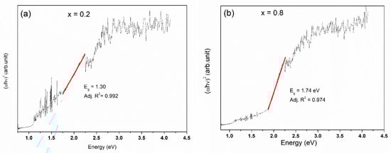
Figure 6.
Plot of (αhν)2 against photon energy (hν) for samples (a) Cu2ZnSn0.8Si0.2Se4 and (b) Cu2ZnSn0.2Si0.8Se4.
The Eg values for Cu2Zn(Sn0.8Si0.2)Se4 and Cu2Zn(Sn0.2Si0.8)Se4 were 1.30 and 1.74 eV, respectively. These results show a good agreement with the values determined theoretically and experimentally for the limit and intermediate phases, corresponding to ~0.90 eV for Cu2ZnSnSe4 [28,29], ~2.2 eV for Cu2ZnSiSe4 [16,30,31] and ~1.7 eV for Cu2ZnSn0.5Si0.5S4 [4]. Chen et al. reported that the I2-II-IV-VI4 semiconductors of the kieserite, stannite, and wurtz-stannite families present the following band structure characteristics: (i) semiconductors usually in Γ point present direct band gaps, (ii) The top valence band considers antibonding p-d hybridization between the group-VI anion and group-I cation as the main constituent; (iii) the bottom conduction band considers the antibonding s-s and s-p hybridization between the group-IV cation and group-VI anion as the main constituent, except for those containing Si, and group-I and -II cations also have significant contributions to the bottom conduction band as well as Si and group-VI anions [32,33].
The results of our study show that partially replacing tin atoms with silicon (from x = 0.2 to x = 0.8) generates a shift towards higher energy; this implies an increase in the bandgap gap as the size of the IVA group cation decreases (Sn4+:0.55 Å to Si4+:0.26 Å). This would favor s-s and s-p level repulsion between the elements of groups IV and VI, causing the minimum of the antibonding conduction band to decrease from Cu2ZnSn0.2Si0.8S4 to Cu2ZnSn0.8Si0.2S4.
3.3. Electrical Properties
The Van-der-Pauw technique is used to measure the electrical properties at room temperature (R.T.). The density (ρ) was calculated using the mass and dimensions of the sample, which corresponded to an average pellet density of ~89% (experimental density/crystallographic density). Electrical conductivity (σ), mobility (m), and carrier concentration (n) measurements of Cu2Zn(Sn0.8Si0.2)Se4 revealed p-type conductivity, which is consistent with previous reports on Cu-deficient Cu2ZnSnSe4 (with different Zn/Sn ratios) and Mg-, Ag-, and In-doped Cu2ZnSnSe4 phases [14,34,35,36,37]. The Hall coefficients of Cu2Zn(Sn0.8Si0.2)Se4 were positive at R.T with a carrier concentration of ~+3.50 × 10⁻¹⁹ cm−3 (in this work). The electrical hole mobility of Cu2Zn(Sn0.8Si0.2)Se4 (2.64 cm2/V·s) was smaller than the value reported for Mg-doped Cu2ZnSnSe4. However, this value is comparable to the mobilities observed for the Cu-deficient Cu2ZnSnSe4. Electrical mobility is an important property for evaluating electrical behavior. The electrical conductivity σ in the Ar atmosphere of Cu2Zn(Sn0.8Si0.2)Se4 was ~13.2 S·cm−1 at 298 K. This value is approximately two times higher than that of Cu2ZnSnSe4, as reported by Kuo D.-H. et al. (~7.20 S·cm−1) at 300 K. These values are also comparable to those of Cu2Zn(Sn0.3In0.6)Se4 systems (~10.4 S·cm−1 at R.T.) [14]. The carrier concentration n of Cu2Zn(Sn0.8Si0.2)Se4 is approximately ten times higher than that of Mg-doped Cu2ZnSnSe (~+10−18) and is comparable to the carrier concentration n of Cu2ZnSnSe4 with different Sn/Zn chemical ratios at 300 K (~+8.29 × 10⁻¹⁸ to +2.02 × 10⁻¹⁹ cm−3) [13,34]. This indicates that σ and n are sensitive to the Sn/Si ratio. The above-mentioned electrical properties indicate semiconductor behavior. Electrical measurements by complex impedance and Dc methods on Cu2Zn(Sn1−xSix)S4 (x = 0.1 and 0.4) showed semiconductor behavior in temperature range of 160–300 K [37]. Theoretical calculations suggest that among the various defects formed in CZTX (X = S, Se), copper vacancies (VCu and VZn) and antisite defects (CuZn, CuSn, and ZnSn) are the dominant cause of intrinsic p-type [33,38,39].
4. Conclusions
Solid Cu2ZnSn1−xSixSe4 (0.2 ≤ x ≤ 0.8) phases were obtained by conventional solid-state synthesis, and their chemical compositions were confirmed by the SEM-EDS technique. X-ray powder diffraction and Rietveld refinement showed a phase transition between wurtz-stannite and stannite as the amount of silicon in the substitution increased. The Raman spectrum confirmed the phase transition owing to changes in the dominant signals that exhibited different crystalline structures. The samples were single-phase, with x < 0.3. In all other samples, two phases coexisted: a tetragonal stannite structure () and an orthorhombic wurtzite (). Electrical measurements indicate a p-type semiconductor behavior, and the band gap values increase with increasing amounts of silicon. These results generate great interest in these materials due to their potential applications as solar absorbers or semiconductor materials.
Supplementary Materials
The following supporting information can be downloaded at: https://www.mdpi.com/article/10.3390/inorganics11010007/s1, Figure S1: Backscattered images for Cu2ZnSn1−xSixSe4, 0.2 ≤ x ≤ 0.8 (a–e).
Author Contributions
Conceptualization, A.G. and S.M.; Methodology and experiments S.M., P.B. and A.G.; electrical measurements, A.G. and P.V.-G.; Raman Analysis P.V.-G.; project administration, S.M. All authors have read and agreed to the published version of the manuscript.
Funding
This work was supported by Fondecyt de Iniciación No. 11200126. The authors thank FONDEQUIP grant EQM140142 for Raman Witec Alpha 300 equipment and the Unidad de Equipamiento Científico “MAINI-UCN” of the Universidad Católica del Norte for the generation of diffuse reflectance spectroscopy data through the FONDEQUIP UV-VIS-NIR grant EQM160120.
Data Availability Statement
Not applicable.
Conflicts of Interest
The authors declare no conflict of interest.
References
- Kumar, J.; Ingole, S. Tailoring the surface morphology of Cu2ZnSnS4 thin films for photovoltaic application. Mater. Sci. Semicond. Process. 2019, 93, 173–181. [Google Scholar] [CrossRef]
- Sun, K.; Yan, C.; Liu, F.; Huang, J.; Zhou, F.; Stride, J.A.; Green, M.; Hao, X. Over 9% Efficient Kesterite Cu2ZnSnS4 Solar Cell Fabricated by Using Zn1–xCdxS Buffer Layer. Adv. Energy Mater. 2016, 6, 1600046. [Google Scholar] [CrossRef]
- Ford, G.M.; Guo, Q.; Agrawal, R.; Hillhouse, H.W. Earth abundant element Cu2Zn(Sn1−xGex)S4 nanocrystals for tunable band gap solar cells: 6.8% Efficient device fabrication. Chem. Mater. 2011, 23, 2626–2629. [Google Scholar] [CrossRef]
- Hamdi, M.; Lafond, A.; Guillot-deudon, C.; Hlel, F.; Gargouri, M.; Jobic, S. Crystal chemistry and optical investigations of the Cu2Zn(Sn,Si)S4 series for photovoltaic applications. J. Solid State Chem. 2014, 220, 232–237. [Google Scholar] [CrossRef]
- Ramkumar, S.P.; Gillet, Y.; Miglio, A.; van Setten, M.J.; Gonze, X.; Rignanese, G.-M. First-principles investigation of the structural, dynamical, and dielectric properties of kesterite, stannite, and PMCA phases of Cu2ZnSnS4. Phys. Rev. B 2016, 94, 224302. [Google Scholar] [CrossRef]
- Lu, X.; Zhuang, Z.; Peng, Q.; Li, Y. Wurtzite Cu2ZnSnS4 nanocrystals: A novel quaternary semiconductor. Chem. Commun. 2011, 47, 3141–3143. [Google Scholar] [CrossRef]
- Paier, J.; Asahi, R.; Nagoya, A.; Kresse, G. Cu2ZnSnS4 as a potential photovoltaic material: A hybrid Hartree-Fock density functional theory study. Phys. Rev. B 2009, 79, 115126. [Google Scholar] [CrossRef]
- Park, J.; Yoo, H.; Karade, V.; Gour, K.S.; Choi, E.; Kim, M.; Hao, X.; Shin, S.J.; Kim, J.; Shim, H.; et al. Investigation of low intensity light performances of kesterite CZTSe, CZTSSe, and CZTS thin film solar cells for indoor applications. J. Mater. Chem. A 2020, 8, 14538–14544. [Google Scholar] [CrossRef]
- Tseberlidis, G.; Trifiletti, V.; Vitiello, E.; Husien, A.H.; Frioni, L.; Da Lisca, M.; Alvarez, J.; Acciarri, M.; Binetti, S.O. Band-Gap Tuning Induced by Germanium Introduction in Solution-Processed Kesterite Thin Films. ACS Omega 2022, 7, 23445–23456. [Google Scholar] [CrossRef]
- Kumar, J.; Ingole, S. Optical phonons in pentanary compound (AgxCu1−x)2ZnSnS4 semiconductor: A raman study. J. Alloys Compd. 2021, 865, 158113. [Google Scholar] [CrossRef]
- Guc, M.; Izquierdo-Roca, V.; Pérez Rodríguez, A.; Gurieva, G.; Levcenko, S.; Schorr, S.; Arushanov, E. Raman spectra of wurtzstannite quaternary compounds. Phys. Status Solidi C 2013, 10, 1075–1078. [Google Scholar] [CrossRef]
- Scragg, J.J.S.; Choubrac, L.; Lafond, A.; Ericson, T.; Platzer-Björkman, C. A low-temperature order-disorder transition in Cu2ZnSnS4 thin films. Appl. Phys. Lett. 2014, 104, 41911. [Google Scholar] [CrossRef]
- Kuo, D.-H.; Wubet, W. Mg dopant in Cu2ZnSnSe4: An n-type former and a promoter of electrical mobility up to 120 cm2 V−1 s−1. J. Solid State Chem. 2014, 215, 122–127. [Google Scholar] [CrossRef]
- Kuo, D.-H.; Tsega, M. Electrical conduction and mobility enhancement in p-type In-doped Cu2ZnSnSe4 bulks. Jpn. J. Appl. Phys. 2014, 53, 35801. [Google Scholar] [CrossRef]
- Vishwakarma, M.; Varandani, D.; Shivaprasad, S.M.; Mehta, B.R. Structural, optical, electrical properties and energy band diagram of Cu2ZnSiS4 thin films. Sol. Energy Mater. Sol. Cells 2018, 174, 577–583. [Google Scholar] [CrossRef]
- Schleich, D.M.; Wold, A. Optical and electrical properties of quarternary chalcogenides. Mater. Res. Bull. 1977, 12, 111–114. [Google Scholar] [CrossRef]
- Kuo, D.-H.; Tsega, M. Hole mobility enhancement of Cu-deficient Cu1.75Zn(Sn1−xAlx)Se4 bulks. J. Solid State Chem. 2013, 206, 134–138. [Google Scholar] [CrossRef]
- Cancino-Gordillo, F.E.; Cab, J.V.; Pal, U. Structure and transport behavior of hydrothermally grown phase pure Cu2ZnSn1−xGexS4 (x = 0.0, 0.3) nanoparticles. Appl. Surf. Sci. 2022, 571, 151261. [Google Scholar] [CrossRef]
- Chen, J.; Li, W.; Yan, C.; Huang, S.; Hao, X. Studies of compositional dependent Cu2Zn(GexSn1−x)S4 thin films prepared by sulfurizing sputtered metallic precursors. J. Alloys Compd. 2015, 621, 154–161. [Google Scholar] [CrossRef]
- Peng, X.; Zhang, S.; Xiang, Y. Solvothermal synthesis of Cu2Zn(Sn1−xGex)S4 and Cu2(Sn1−xGex)S3 nanoparticles with tunable band gap energies. J. Alloys Compd. 2015, 640, 75–81. [Google Scholar] [CrossRef]
- Syrbu, N.N.; Zalamai, V.; Guc, M.; Levcenko, S.; Dorogan, A.; Arushanov, E. Birefringence of Cu2ZnSiSe4 single crystals. J. Alloys Compd. 2015, 635, 188–193. [Google Scholar] [CrossRef]
- Shannon, R.D. Revised effective ionic radii and systematic studies of interatomic distances in halides and chalcogenides. Acta Crystallogr. Sect. A 1976, 32, 751–767. [Google Scholar] [CrossRef]
- Gürel, T.; Sevik, C.; Çağın, T. Characterization of vibrational and mechanical properties of quaternary compounds Cu2ZnSnS4 and Cu2ZnSnSe4 in kesterite and stannite structures. Phys. Rev. B 2011, 84, 205201. [Google Scholar] [CrossRef]
- Fontané, X.; Izquierdo-Roca, V.; Saucedo, E.; Schorr, S.; Yukhymchuk, V.O.; Valakh, M.Y.; Pérez-Rodríguez, A.; Morante, J.R. Vibrational properties of stannite and kesterite type compounds: Raman scattering analysis of Cu2(Fe,Zn)SnS4. J. Alloys Compd. 2012, 539, 190–194. [Google Scholar] [CrossRef]
- Levcenco, S.; Dumcenco, D.O.; Wang, Y.P.; Wu, J.D.; Huang, Y.S.; Arushanov, E.; Tezlevan, V.; Tiong, K.K. Photoluminescence and Raman scattering characterization of Cu2ZnSiQ4 (Q = S, Se) single crystals. Opt. Mater. 2012, 34, 1072–1076. [Google Scholar] [CrossRef]
- Tauc, J.; Menth, A. States in the gap. J. Non. Cryst. Solids 1972, 8–10, 569–585. [Google Scholar] [CrossRef]
- Moris, S.; Manríquez, V.; Barahona, P.; Galdámez, A.; Valencia-Gálvez, P.; Galdamez, A.; Manriquez, V.; Valencia-Galvez, P. Electrical and optical properties of p-type Ag0.3Cu0.7InQ2 chalcopyrite semiconductors. Lett. Chalcogenide 2018, 15, 615–623. [Google Scholar]
- Ahn, S.; Jung, S.; Gwak, J.; Cho, A.; Shin, K.; Yoon, K.; Park, D.; Cheong, H.; Yun, J.H. Determination of band gap energy (Eg) of Cu2ZnSnSe4 thin films: On the discrepancies of reported band gap values. Appl. Phys. Lett. 2010, 97, 21905. [Google Scholar] [CrossRef]
- Altosaar, M.; Raudoja, J.; Timmo, K.; Danilson, M.; Grossberg, M.; Krustok, J.; Mellikov, E. Cu2Zn1–x Cdx Sn(Se1–ySy)4 solid solutions as absorber materials for solar cells. Phys. Status Solidi A 2008, 205, 167–170. [Google Scholar] [CrossRef]
- Levcenco, S.; Dumcenco, D.; Huang, Y.S.; Arushanov, E.; Tezlevan, V.; Tiong, K.K.; Du, C.H. Absorption-edge anisotropy of Cu2ZnSiQ4 (Q = S, Se) quaternary compound semiconductors. J. Alloys Compd. 2011, 509, 4924–4928. [Google Scholar] [CrossRef]
- Levcenco, S.; Dumcenco, D.; Huang, Y.S.; Arushanov, E.; Tezlevan, V.; Tiong, K.K.; Du, C.H. Polarization-dependent electrolyte electroreflectance study of Cu2ZnSiS4 and Cu2ZnSiSe4 single crystals. J. Alloys Compd. 2011, 509, 7105–7108. [Google Scholar] [CrossRef]
- Chen, S.; Gong, X.G.; Walsh, A.; Wei, S.-H. Electronic structure and stability of quaternary chalcogenide semiconductors derived from cation cross-substitution of II-VI and I-III-VI2 compounds. Phys. Rev. B 2009, 79, 165211. [Google Scholar] [CrossRef]
- Chen, S.; Walsh, A.; Gong, X.-G.; Wei, S.-H. Classification of Lattice Defects in the Kesterite Cu2ZnSnS4 and Cu2ZnSnSe4 Earth-Abundant Solar Cell Absorbers. Adv. Mater. 2013, 25, 1522–1539. [Google Scholar] [CrossRef]
- Tsega, M.; Kuo, D.-H. The performance of the donor and acceptor doping in the Cu-rich Cu2ZnSnSe4 bulks with different Zn/Sn ratios. Solid State Commun. 2013, 164, 42–46. [Google Scholar] [CrossRef]
- Saragih, A.D.; Wubet, W.; Abdullah, H.; Abay, A.K.; Kuo, D.-H. Characterization of Ag-doped Cu2ZnSnSe4 bulks material and their application as thin film semiconductor in solar cells. Mater. Sci. Eng. B 2017, 225, 45–53. [Google Scholar] [CrossRef]
- Kuo, D.-H.; Wubet, W. Mg dopant in Cu2SnSe3: An n-type former and a promoter of electrical mobility up to 387 cm2 V−1 s−1. J. Solid State Chem. 2014, 218, 44–49. [Google Scholar] [CrossRef]
- Hamdi, M.; Chrif, B.; Lafond, A.; Louati, B.; Guillot-Deudon, C.; Hlel, F. Electrical properties of Cu2Zn(Sn1−xSix)S4 (x = 0.1, x = 0.4) compounds for absorber materials in solar-cells. J. Alloys Compd. 2015, 643, 129–136. [Google Scholar] [CrossRef]
- Tsega, M.; Kuo, D.-H. Defects and Its Effects on Properties of Cu-Deficient Cu2ZnSnSe4 Bulks with Different Zn/Sn Ratios. Appl. Phys. Express 2012, 5, 91201. [Google Scholar] [CrossRef]
- Chen, S.; Yang, J.-H.; Gong, X.G.; Walsh, A.; Wei, S.-H. Intrinsic point defects and complexes in the quaternary kesterite semiconductor Cu2ZnSnS4. Phys. Rev. B 2010, 81, 245204. [Google Scholar] [CrossRef]
Disclaimer/Publisher’s Note: The statements, opinions and data contained in all publications are solely those of the individual author(s) and contributor(s) and not of MDPI and/or the editor(s). MDPI and/or the editor(s) disclaim responsibility for any injury to people or property resulting from any ideas, methods, instructions or products referred to in the content. |
© 2022 by the authors. Licensee MDPI, Basel, Switzerland. This article is an open access article distributed under the terms and conditions of the Creative Commons Attribution (CC BY) license (https://creativecommons.org/licenses/by/4.0/).