
SCAPS-1D Simulation for Device Optimization to Improve Efficiency in Lead-Free CsSnI3 Perovskite Solar Cells

1
Department of Hydrogen and Renewable Energy, Kyungpook National University, Daegu 41566, Republic of Korea
2
KNU Advanced Material Research Institute, Kyungpook National University, Daegu 41566, Republic of Korea
*
Author to whom correspondence should be addressed.
Inorganics 2024, 12(4), 123; https://doi.org/10.3390/inorganics12040123
Submission received: 26 March 2024
/
Revised: 16 April 2024
/
Accepted: 19 April 2024
/
Published: 21 April 2024
Abstract
:In this study, a novel systematic analysis was conducted to explore the impact of various parameters, including acceptor density (NA), individual layer thickness, defect density, interface defect density, and the metal electrode work function, on efficiency within the FTO/ZnO/CsSnI3/NiOx/Au perovskite solar cell structure through the SCAPS-1D (Solar Cell Capacitance Simulator in 1 Dimension) simulation. ZnO served as the electron transport layer (ETL), CsSnI3 as the perovskite absorption layer (PAL), and NiOx as the hole transport layer (HTL), all contributing to the optimization of device performance. To achieve the optimal power conversion efficiency (PCE), we determined the ideal PAL acceptor density (NA) to be 2 × 1019 cm−3 and the optimal thicknesses to be 20 nm for the ETL (ZnO), 700 nm for the PAL (CsSnI3), and 10 nm for the HTL (NiOx), with the metal electrode remaining as Au. As a result of the optimization process, efficiency increased from 11.89% to 23.84%. These results are expected to contribute to the performance enhancement of eco-friendly, lead-free inorganic hybrid solar cells with Sn-based perovskite as the PAL.
1. Introduction
Because of environmental concerns and resource scarcity, it is considered difficult for energy production based on fossil fuels to be sustainable [1,2]. Solar energy has emerged as a promising alternative over the past few decades, offering a solution to these challenges [3,4]. In particular, perovskites, with their superior properties, have gained attention as a leading contender for next-generation solar cells [5,6]. The chemical formula of perovskite is ABX3, where A comprises large cations (Cs+, NH2CH3NH2+, CH3NH3+), B comprises divalent cations (Pb2+, Sn2+), and X comprises monatomic halogen anions (I−, Br−, Cl−) [7,8]. Due to their long diffusion lengths and high absorption coefficients (104 cm−1), along with the benefits of flexibility, lightweight, and transparency, these materials hold economic advantages, spurring extensive research in the field [9,10,11].
PSCs have demonstrated rapid performance improvement, achieving efficiencies comparable to conventional solar cells, with a remarkable efficiency of 26.1% reported in 2023 [12]. Moreover, the parameters of the maximum theoretical limit (SQ-limit) employing the CH3NH3PbI3-xCLx absorber (Eg~1.55 eV) have been reported as follows: current density (JSC) is 27.20 mA/cm2, open-circuit voltage (VOC) is 1.28 V, fill factor (FF), and power conversion efficiency (PCE) is 90.2% and 31.4%, respectively [13,14]. This demonstrates the potential for the further advancement of perovskite solar cells, indicating a promising future.
However, several challenges remain unresolved for PSCs, including the development of commercially feasible next-generation perovskite materials and advancements in manufacturing technology [15,16]. Additionally, hybrid perovskites, such as methylammonium lead triiodide (MAPbI3) and formamidinium lead triiodide (FAPbI3), which have been extensively studied, exhibit poor stability against heat and moisture [17,18]. As a result, the fabrication of hybrid PSCs requires careful environmental control, such as glove boxes or drying chambers [19,20]. Currently, due to these drawbacks of organic-based perovskites, there is an increasing amount of research being conducted on photovoltaic solar cells that utilize inorganic perovskites [21,22,23].
Therefore, in this study, we selected an inorganic perovskite material to fabricate an all-inorganic PSC. Among them, one of the primary concerns in all-inorganic perovskites is the use of lead (Pb) in the PAL of most high-efficiency photovoltaic cells (PVs) [24,25,26]. Lead-based perovskites produce harmful by-products like PbI2 when decomposed, which can cause oxidative stress when exposed to the human body, potentially harming the nervous, reproductive, blood, and kidney systems [27,28]. As an alternative to solving these issues, research into tin-based (Sn-based) perovskites has emerged as a new area of focus [29]. This tin-based inorganic perovskite (CsSnX3) provides benefits such as a bandgap close to 1.4 eV, high mobility, and a high absorption coefficient (greater than 105 cm−1) [30,31].
In particular, CsSnI3 has a bandgap of 1.3–1.4 eV and exhibits a high absorption coefficient of 104 cm−1 in the visible range [32]. Additionally, its low exciton binding energy (10–20 meV) facilitates easier carrier separation compared to typical organic absorbers [33]. In addition, it has the advantage of superior thermal stability with a melting point of 451 °C, which is higher than that of conventional perovskites such as MASnI3 and FASnI3, which have a melting point of 200 °C [34]. Because of these characteristics, CsSnI3 has demonstrated the highest experimental efficiency of 10.1% among reported Pb-free Sn-based perovskite materials [35].
As for ZnO, used as the electron transport layer (ETL) material, it is environmentally friendly and exhibits high carrier mobility [36]. With a wide bandgap (3.3 eV) and a significant exciton binding energy, ZnO is being studied as one of the most interesting ETL materials [37,38]. Especially for ZnO single nanowires, they feature electron mobility of up to ~1000 cm2/V·s and can be doped with both n-type and p-type materials [39].
Regarding NiOx, which serves as the hole transport layer (HTL) material, it exhibits a large bandgap (>3.5 eV) with superior transparency in the visible range [40]. This characteristic can minimize losses such as charge recombination, enhance charge transport, and provide optimal energy-level alignment with various photoactive absorbers due to its sufficient conductivity and chemical stability [38,41].
Based on these properties, we selected CsSnI3 as PAL, ZnO as ETL, NiOx as HTL and constructed an environmentally friendly Sn-based Pb-free PSC device (FTO/ZnO/CsSnI3/NiOx/Au). However, there are few studies systematically analyzing the influence of each parameter (such as acceptor density, layer thickness, interface defect density, and metal electrode work function) in the FTO/ZnO/CsSnI3/NiOx/Au structure [42].
Therefore, in this study, based on the consideration of each parameter, we systematically analyzed the effect of key parameters, such as acceptor density, layer thickness, defect density, interfacial defect density, and metal electrode work function, on the performance of photovoltaic solar cells and proposed an optimized solar cell structure, FTO/ZnO/CsSnI3/NiOx/Au, which is a completely inorganic device architecture.
Of course, practically, in the experimental phase, controlling interface defects is crucial due to their significant impact on device performance. Such defects can arise from material inhomogeneity, varying process conditions, and the nature of surface treatments [43,44]. Notably, material inhomogeneity, particularly the intrinsic surface defects of zinc oxide, can lead to severe carrier recombination, as highlighted in reference [45]. Therefore, for the scope of this simulation research, we are concentrating on the alteration of specific parameters—the density of interface defects and overall defect density—to determine their impact on the power conversion efficiency (PCE) of the device. These parameters need to be closely studied and adjusted as necessary before we proceed with full-scale practical experiments.
2. Results and Discussion
2.1. Simulation under Initial Conditions
The device performance was analyzed based on key parameters such as open-circuit voltage (VOC), short-circuit current density (JSC), fill factor (FF), and power conversion efficiency (PCE). Importantly, the FF was calculated using Equation (1), as reported in references [46,47].
The parameter for power conversion efficiency (PCE) was determined by the following in Equation (2):
where ISC is the short-circuit photocurrent, and Pin is the input power. The quantum efficiency (QE) is the ratio of the number of charge carriers collected by the solar cell to the number of incident photons at a specific energy, which is calculated as follows in Equation (3) [48].
The initial simulation results for the current density–voltage (J–V) plot and the quantum efficiency (QE) curve for FTO/ZnO/CsSnI3/NiOx/Au PSC are depicted in Figure 1a,b, respectively. The parameters for the current density–voltage (J–V) characteristics, including VOC, JSC, FF, and PCE, were 1.01 V, 15.55 mA/cm2, 75.78%, and 11.89%, respectively. The initial efficiency obtained was low at 11.89%, and accordingly, the levels of parameters were adjusted to investigate the effects of VOC, JSC, and FF on PCE for the optimization of this perovskite solar cell device.
2.2. Efficiency Variation Depending on Acceptor Density (NA) of PAL
Figure 2 illustrates the variation in VOC, JSC, FF, and PCE with PAL acceptor density (NA) within the range of 2 × 10¹⁹ to 1021 cm−3. The initial setting value was 1 × 1020 cm−3, referenced to the optimal value determined in a prior study, while 2 × 1019 cm−3 represents the minimum NA providing a certain PV response [49,50]. The PCE exhibited an overall decreasing trend as NA increased, with a PCE of 22.05% when NA was 2 × 1019 cm−3, in contrast to a PCE of 0.53% when NA was 1 × 1021 cm−3, indicating the significant impact of NA on PCE. JSC and FF exhibited similar trends to PCE, while VOC increased up to 7 × 1019 cm−3 before decreasing. This increase in VOC is attributed to the fermi level (Ef) approaching the valence band (VB) due to increased acceptor doping [51]. Subsequently, the increase in charge carriers led to a decrease in VOC. Two predominant factors contributed to the efficiency decrement with increasing NA; firstly, this included the increase in sheet resistance [52,53]. With the increase in doping density, the sheet resistance of PAL for NA in p-type perovskite materials increases, impeding hole mobility to HTL, accelerating the recombination of photo-generated carriers, decreasing the generation of electron-hole pairs, and resulting in a decrease in efficiency owing to a reduction in the minority carrier concentration, mobility, and diffusion length. Equation (4) describes the decrement in saturation current (IO) with increasing NA [54].
where IO is the saturation current, ni is the intrinsic concentration, A is the diode quality factor, q is the elementary charge, NA and ND are the acceptor and donor charge concentrations, Le and Lh are the electron and hole diffusion length, and De and Dh are diffusion coefficient, respectively.
The secondary causative factor is the incidence of Auger recombination due to high doping concentrations [55,56]. In devices where the concentration exceeds 1018 cm−3, dopants trigger Auger recombination, ultimately leading to a reduction in the performance parameters of the photovoltaic device.
Consequently, by setting the optimal NA value of 2 × 1019 cm−3 for the PAL, JSC, and PCE achieved a notable enhancement from 15.55 mA/cm2 to 27.58 mA/cm2 and from 11.89% to 22.05%, respectively. The other parameters were maintained consistent with previous settings. According to a previously published paper, the optimal NA value of 2 × 1019 cm−3 aligns with CsSnI3, typically exhibiting a maximum p-type doping concentration of 1019 to 1020 cm−3 even in the undoped case at room temperature, and the addition of Sn can increase the NA value [57]. This occurrence is ascribed to the presence of hydrogen anions in Sn-rich environments, facilitating a shift in the Fermi level (Ef) towards the valence band maximum (VBM) and considerably increasing the doped hole concentration [58]. The NA value of 2 × 1019 cm−3 selected in this study aligns with the optimal values previously reported at 1019 and 7 × 1019 cm−3 [59,60].
2.3. Optimization of Each Layer’s Thickness
Each layer of the PSC serves a distinctive role in the performance of the cell, so it is important to adjust the thickness of each layer for optimal cell performance. The optimization of layer thickness was executed by preserving the uniform thickness for two layers and varying the thickness of the residual layers.
2.3.1. Optimization of ZnO Thickness
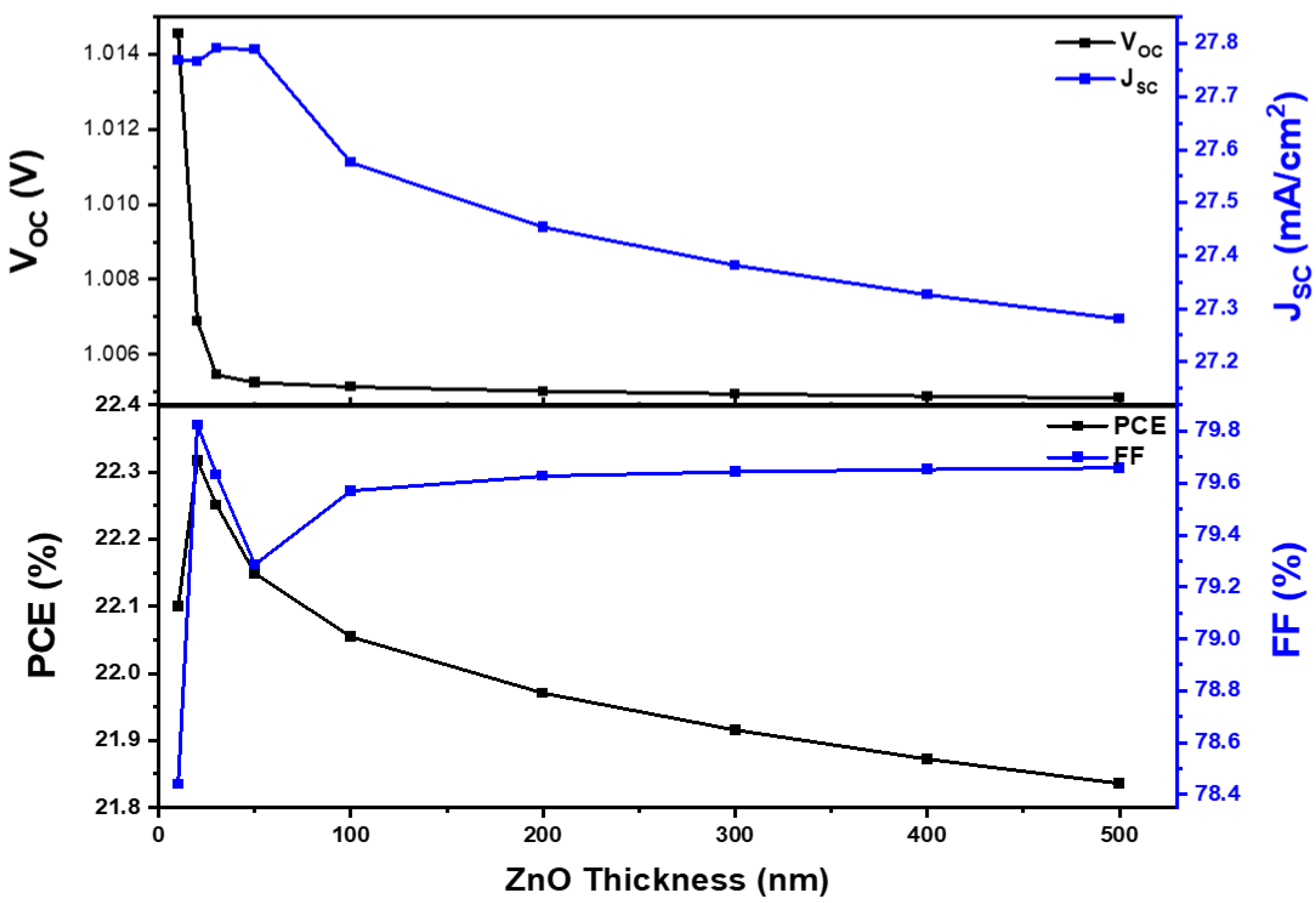
ZnO is employed as an electron transport layer (ETL) material in the n-i-p structure as the initial substance to be exposed to incoming light. For the initial device fabrication, optimizing the thickness of ZnO is important. Thus, referencing the 16 nm and 20 nm ZnO coating thicknesses fabricated using spin-coating in papers [61,62], our study conducted optimization within the range of 10 to 500 nm for ZnO coating. The graph in Figure 3 describes the impact of ZnO thickness on VOC, JSC, FF, and PCE. As the thickness of ZnO increased from 10 nm to 20 nm, PCE increased from 22.05% to 22.32%. The low PCE at a ZnO thickness of 10 nm can be attributed to insufficient layer thickness for effective electron extraction and transport, leading to inefficiencies in charge collection, resulting in lower FF and PCE [63,64]. In the thickness range of 20 nm to 50 nm, the FF value exhibited an overall decrease followed by an increase thereafter. This phenomenon was ascribed to the relatively small decrease in JSC compared to VOC at this thickness. Similar observations were reported in a previous study [65]. Furthermore, the decrease in PCE with increasing thickness is associated with the acceleration of electron-hole pair recombination due to the surface roughness with thicker layers [66]. This precipitates an increase in series resistance, causing a reduction in JSC and VOC. Therefore, we derived the conclusion that a thinner ETL thickness leads to an increase in efficiency. Based on this conclusion, we set the optimal thickness to 20 nm.
2.3.2. Optimization of PAL Thickness
Upon light incidence on the absorption stratum of a solar cell, electron-hole pairs are generated. For effective operation of the solar cell, it is important that these pairs reach each electrode without recombination [67]. To achieve this, optimizing the thickness of the perovskite absorption layer (PAL) is essential. When the PAL thickness is excessively thick, it increases the time required for the absorption and conversion of light energy, leading to recombination [68]. Conversely, an excessively thinner PAL can impede light absorption, decreasing the current density [69]. To find the optimum thickness, optimization was performed in the range of 100 to 1200 nm. The graph in Figure 4 illustrates the influence of PAL thickness on VOC, JSC, FF, and PCE. VOC, JSC, and PCE predominantly exhibited an overall increasing trend, while FF increased in the range of 100 to 200 nm and then decreased from 200 to 1200 nm. The initial increase in FF was attributed to the efficient charge transport with increasing thickness, while the subsequent decrease was due to a reduction in shunt resistance and an increase in series resistance [70]. Furthermore, PCE increased in the range of 100 to 700 nm, reaching its highest efficiency of 22.64% at a thickness of 700 nm. This was due to the substantial photon absorption by PAL, resulting in the generation of the most electron-hole pairs [71]. However, from 700 to 1200 nm, PCE decreased due to the resistance caused by recombination [72,73].
Equation (5) depicts the mathematical relation between the thickness and absolute absorption rate of the absorber [74]. By employing this equation, the absolute absorption rate of the absorber can be computed, facilitating the determination of the optimal thickness of PAL.
Here, Rabsorber is the absorber resistance, p is the resistance of the PAL, t is the thickness of PAL, and A is the cross-sectional area. This results in Equation (5); as the PAL thickness increases, the absorber resistance rises. This phenomenon generally leads to an increase in VOC, JSC, and FF values. However, the increase in absorber thickness also enhances the photon energy absorption rate [75]. Considering these electrical and optical property changes, an optimal PCE at 22.64% was achieved when the absorber thickness was 700 nm.
2.3.3. Optimization of NiOx Thickness
The hole transport layer (HTL) serves a crucial role in enhancing the transport of charge carriers (holes) and prevents direct contact between the PAL and anode through capping [76,77]. Figure 5a illustrates the influence of NiOx thickness within the range of 10 to 500 nm on VOC, JSC, FF, and PCE. The peak efficiency of 22.76% was achieved at the smallest thickness of 10 nm, while PCE decreased as the thickness increased, reaching its lowest efficiency of 19.1% at the maximum thickness of 500 nm. This result was primarily attributed to the increase in HTL thickness, causing an increase in the series resistance of the solar cell [78]. Consequently, it became challenging for holes to reach the anode, resulting in recombination and causing a decrease in VOC, JSC, FF, and overall PCE.
Following NiOx thickness optimization, the optimal thickness for ZnO and CsSnI3 were determined to be 20 nm and 700 nm, respectively. As shown in Figure 5b, the corresponding values for VOC, JSC, FF, and PCE were 1.01 V, 28.02 mA/cm2, 80.5%, and 22.76%, respectively. The PCE graphs based on the thickness of each layer demonstrated that the thickness of each layer had a substantial impact on the performance of the PSC.
2.4. Optimization of PAL Defect Density and Interface Defect Density
The defect density typically increases the recombination of photogenerated carriers at both the bulk material and interface defects, leading to an increase in the quasi-saturation current density (J0) and consequently reducing both JSC and VOC [79,80]. Therefore, to investigate the effect of defect density on Jsc, Voc, FF, and PCE, simulations were conducted for the defect density of the PAL. Figure 6a demonstrates the influence of the PAL defect density varying from 1011 to 1018 cm−3 on VOC, JSC, FF, and PCE.
The efficiency remained stable within the initial defect density range of 1011~1015 cm−3; however, a sharp decrease in efficiency was observed from 1016 cm−3 onwards. This phenomenon can be attributed to the increase in defect density, which leads to an increase in recombination current and accelerated carrier recombination [81].
As described in Figure 6b, the graph of bulk recombination current density caused by the PAL defect density confirmed the increase in the recombination current at a defect density of 1016 cm−3. Ultimately, the lowest efficiency of 19.24% was observed at the maximum value of 1018 cm−3. This was attributed to a degradation in film quality due to the surge in defect density, leading to an accelerated recombination rate and shortened carrier lifetime, and consequently leading to decreased efficiency [82,83]. Based on these results, the optimal defect density was adjusted to the conventional value of 1014 cm−3, thereby maintaining the original efficiency of 22.76%. These results also exhibited a similar tendency as those reported in previously conducted research [84,85].
The performance of the device significantly varies depending on the defect density of the interface layer, as shown in Figure 7a,b. Figure 7a,b illustrate the impact of defect density on VOC, JSC, FF, and PCE for the ZnO/PAL interface and PAL/NiOx interface, respectively, in the range of 108 to 1020 cm−3.
As the defect density increases at both interfaces, the PCE initially remains stable without significant changes. However, for the ZnO/PAL interface, the PCE begins to gradually decrease, starting from 1011 cm−3 in Figure 7a. In contrast, in the case of the PAL/NiOx interface, efficiency remained within the range of 108 to 1015 cm−3, but it began to decrease sharply, starting from 1016 cm−3 in Figure 7b. This decrease in efficiency is attributed to defects acting as recombination centers, leading to a reduction in charge carrier density as the defect density increases [86]. The sharp decrease at a certain interface defect density is attributed to a rapid decline in photon absorption when exceeding a specific Nt value at each interface [87]. As a result, PCE was enhanced from 22.76% to 23.84% by setting the optimal interface defect density for both interfaces at 108 cm−3.
2.5. Optimization of Metal Electrode Work Function
For the design of high-performing solar cells, the choice of suitable electrodes is critical. For this part, experiments were carried out using metal electrode materials such as Al (4.2 eV), Cu (4.6 eV), Ag (4.7 eV), Fe (4.8 eV), and Au (5.1 eV) [88]. Figure 8 illustrates the influence of metal electrode work functions on VOC, JSC, FF, and PCE. As the work function increased, all parameters exhibited a tendency to increase proportionally. As a result, PCE was lowest at 4.17% for Al, which had the lowest work function of 4.2 eV, while Au, with the highest work function of 5.1 eV, achieved an optimal efficiency of 23.84%. A reason for the decrease in efficiency as the work function of the metal electrodes decreased was due to the increased Schottky barrier impeding hole transport, leading to a decrease in FF [89]. Furthermore, regarding higher work functions mentioned in Ref. [90], such as W (5.22 eV), Ni (5.5 eV), Pt (5.7 eV), Se (5.9 eV), PCE shows saturated behavior indicating the absence of additional chemical interactions between the PAL and these metals (W, Ni, Pt, Se). Based on these results, this study utilized Au as the optimal metal electrode. These findings concur with various simulation results [91,92].
3. Materials and Methods
3.1. Numerical Modeling
The numerical simulations performed in this study were based on the SCAPS-1D (Solar Cell Capacitance Simulation in 1 Dimension) (ver. 3.3.11) simulator. This computational tool, developed by Dr. M. Burgelman of the University of Gent in Belgium, enables the design and simulation of up to seven heterojunction layers [93]. The simulations were based on Poisson’s Equation (6) and the continuity Equations (7) and (8) for each electron and hole, respectively [94,95].
In this equation, is the dielectric constant, q is the charge of an electron, G is the generation rate, D is the diffusion coefficient, ψ is the electrostatic potential, E is the electric field, and p(x), n(x), pt(x), and nt(x) are free holes, free electrons, trapped holes, and trapped electrons, respectively. N+d refers to doping concentration-like ionized donors, N−a represents doping concentration-like ionized acceptors, and x is the direction along the thickness. In this study, following the standard test conditions (STC), the spectrum used in all simulations was the AM1.5G spectrum, the incident light power was set at 1000 W/m2, the operating point voltage set to 0 V, and the temperature was set at 300 K [96].
3.2. Device Structure
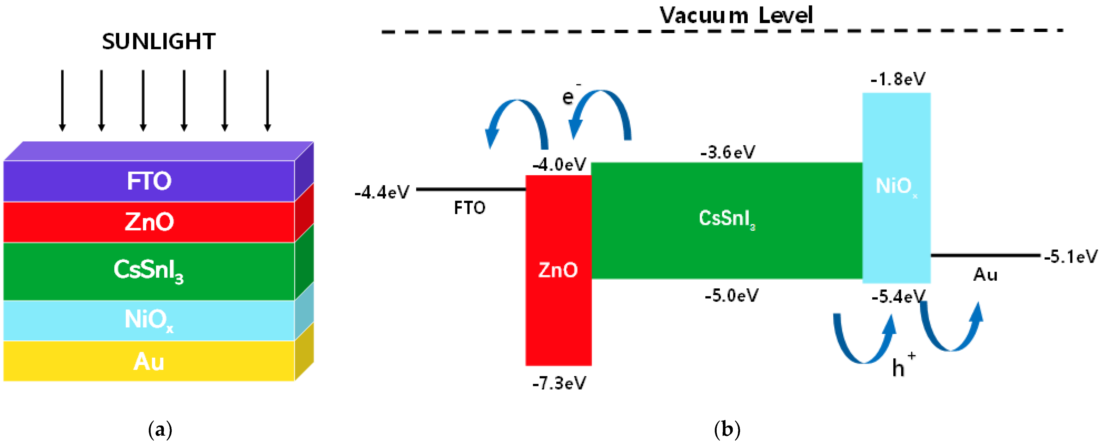
Figure 9a illustrates a solid-state planar heterojunction p-i-n structure device composed of FTO/ZnO/CsSnI3/NiOx/Au. In this device, the perovskite material (CsSnI3) is sandwiched between the n-type hole transport layer (HTL) NiOx and the p-type electron transport layer (ETL) ZnO, with Au serving as the metal electrode. Figure 9b presents a simplified flat band energy diagram of the PSC. The work functions of FTO and Au are 4.4 eV and 5.1 eV, respectively [97,98]. The highest occupied molecular orbital (HOMO) and lowest unoccupied molecular orbital (LUMO) levels for ZnO, CsSnI3, and NiOx were 4.0 eV and 7.3 eV, 3.6 eV and 5.0 eV, and 1.8 eV and 5.4 eV, respectively [99,100,101]. Upon light irradiation, weakly bounded excitons were generated in the PAL of this device. These excitons undergo a dissociation process, rapidly separating into electrons and holes prior to recombination, promoting effective carrier transport within the device [102]. The energy structure depicted in the band diagram in Figure 9b facilitates the efficient movement of electrons and holes in the conduction and valence bands, respectively, significantly influencing the overall performance of the device.
Table 1 presents the initial parameters of each material used in the FTO/ZnO/CsSnI3/NiOx/Au PSC simulations. The initial thicknesses of FTO, ZnO, CsSnI3, and NiOx were 500 nm, 100 nm, 1000 nm, and 30 nm, respectively [103,104,105]. The bandgap and electron affinity for each material are given as follows: FTO (3.2 eV, 4.4 eV), ZnO (3.3 eV, 4.0 eV), CsSnI3 (1.4 eV, 3.6 eV), and NiOx (3.6 eV, 1.8 eV) [106,107,108,109]. For the perovskite absorption layer (PAL), the band-to-band recombination model was maintained at a radiative recombination coefficient of 3 × 10⁻¹¹ cm3 and an Auger capture rate of 1 × 10⁻²⁹ cm6/s for both carriers (electrons and holes) [110,111]. The dielectric permittivity values for each material were 9, 8.656, 9.93, and 10.7, respectively. The thermal velocity of charge carriers (electrons and holes) in all layers was maintained at 107 cm/s. For interfacial layers, the defect type was set as neutral, with a Gaussian energy distribution, and the reference energy level for defect (Et) was set above EV. The capture cross-section for both types of charge carriers (electrons and holes) was 10−19 cm−3, and the total charge carrier density was set at 1.0 × 1011 cm−3. The variations in the parameters are listed in Table 2. Additionally, the band-to-band recombination model was maintained at zero for FTO, ETL, and HTL layers. Furthermore, the tunneling effect was not considered in the simulation.
4. Conclusions
In this study, in the device structure of FTO/ZnO/CsSnI3/NiOx/Au, various parameters, including the acceptor density (NA) of the perovskite absorber layer (PAL), the thickness of each material layer, the defect density of PAL, the interface defect density, and work function of the metal electrode, were optimized. The parameters were optimized such that the NA of the PAL was 2 × 1019 cm−3, the thicknesses of the ETL (ZnO), PAL (CsSnI3), and HTL (NiOx) were 20 nm, 700 nm, and 10 nm, respectively, the PAL defect density was 1014 cm−3, and interface defect density for ZnO/PAL and PAL/NiOx was 108 cm−3. As a result, the performance of the device was enhanced, with VOC, JSC, FF, and PCE improving from 1.01 to 1.05 V, 15.55 to 28.02 mA/cm2, 75.78 to 81.22%, and 11.89 to 23.84%, respectively. This emphasizes the potential for the high-efficiency design of environmentally friendly, lead-free perovskite solar cells based on CsSnI3.
Author Contributions
Conceptualization, H.-J.P. and B.-S.J.; software, H.-J.P. and H.S.; methodology, H.-J.P. and B.-S.J.; formal analysis, H.-J.P., H.S. and B.-S.J.; writing—original draft preparation, H.-J.P.; writing—review and editing, B.-S.J.; supervision, B.-S.J. All authors have read and agreed to the published version of the manuscript.
Funding
This work was supported by the Industrial Technology Innovation Program funded by the Ministry of Trade, Industry & Energy (MOTIE, Korea) [No. 20015778].
Data Availability Statement
The data presented in this study are available upon request from the corresponding author.
Conflicts of Interest
The authors declare no conflicts of interest.
References
- Yao, L. New energy utilization in environmental design and realization. Energy Rep. 2022, 8, 9211–9220. [Google Scholar] [CrossRef]
- Nunes, F.C.; de Jesus Alves, L.; Bitterncourt, P.; Prasad, M.N.V. Nonfossil energy targets for environmental sustainability. In Decarbonization Strategies and Drivers to Achieve Carbon Neutrality for Sustainability; Elsevier: Amsterdam, The Netherlands, 2024; pp. 27–44. [Google Scholar]
- Ashraf, M.; Ayaz, M.; Khan, M.; Adil, S.F.; Farooq, W.; Ullah, N.; Nawaz Tahir, M. Recent trends in sustainable solar energy conversion technologies: Mechanisms, prospects, and challenges. Energy Fuels 2023, 37, 6283–6301. [Google Scholar] [CrossRef]
- Hassan, Q.; Viktor, P.; Al-Musawi, T.J.; Ali, B.M.; Algburi, S.; Alzoubi, H.M.; Al-Jiboory, A.K.; Sameen, A.Z.; Salman, H.M.; Jaszczur, M. The renewable energy role in the global energy Transformations. Renew. Energy Focus 2024, 48, 100545. [Google Scholar] [CrossRef]
- Nie, T.; Fang, Z.; Ren, X.; Duan, Y.; Liu, S. Recent advances in wide-bandgap organic–inorganic halide perovskite solar cells and tandem application. Nano Micro Lett. 2023, 15, 70. [Google Scholar] [CrossRef] [PubMed]
- Bati, A.S.; Zhong, Y.L.; Burn, P.L.; Nazeeruddin, M.K.; Shaw, P.E.; Batmunkh, M. Next-generation applications for integrated perovskite solar cells. Commun. Mater. 2023, 4, 2. [Google Scholar] [CrossRef]
- Qian, J.; Xu, B.; Tian, W. A comprehensive theoretical study of halide perovskites ABX3. Org. Electron. 2016, 37, 61–73. [Google Scholar] [CrossRef]
- Shaw, B.K.; Castillo-Blas, C.; Thorne, M.F.; Gómez, M.L.R.; Forrest, T.; Lopez, M.D.; Chater, P.A.; McHugh, L.N.; Keen, D.A.; Bennett, T.D. Principles of melting in hybrid organic–inorganic perovskite and polymorphic ABX3 structures. Chem. Sci. J. 2022, 13, 2033–2042. [Google Scholar] [CrossRef]
- Jung, H.S.; Han, G.S.; Park, N.G.; Ko, M.J. Flexible perovskite solar cells. Joule 2019, 3, 1850–1880. [Google Scholar] [CrossRef]
- Xie, F.X.; Su, H.; Mao, J.; Wong, K.S.; Choy, W.C. Evolution of diffusion length and trap state induced by chloride in perovskite solar cell. J. Phys. Chem. C 2016, 120, 21248–21253. [Google Scholar] [CrossRef]
- Park, N.G. Methodologies for high efficiency perovskite solar cells. Nano Converg. 2016, 3, 15. [Google Scholar] [CrossRef]
- Lan, Z.R.; Wang, Y.D.; Shao, J.Y.; Ma, D.X.; Liu, Z.; Li, D.; Hou, Y.; Yao, J.; Zhong, Y.W. Surface Passivation with Diaminopropane Dihydroiodide for p-i-n Perovskite Solar Cells with over 25% Efficiency. Adv. Funct. Mater. 2024, 34, 2312426. [Google Scholar] [CrossRef]
- Elumalai, N.K.; Mahmud, M.A.; Wang, D.; Uddin, A. Perovskite solar cells: Progress and advancements. Energies 2016, 9, 861. [Google Scholar] [CrossRef]
- Bimli, S.; Manjunath, V.; Mulani, S.R.; Miglani, A.; Game, O.S.; Devan, R.S. Theoretical investigations of all inorganic Cs2SnI6 double perovskite solar cells for efficiency∼30%. Sol. Energy 2023, 256, 76–87. [Google Scholar] [CrossRef]
- Petrus, M.L.; Schlipf, J.; Li, C.; Gujar, T.P.; Giesbrecht, N.; Müller-Buschbaum, P.; Thelakkat, M.; Bein, T.; Hüttner, S.; Docampo, P. Capturing the sun: A review of the challenges and perspectives of perovskite solar cells. Adv. Energy Mater. 2017, 7, 1700264. [Google Scholar] [CrossRef]
- Ansari, M.I.H.; Qurashi, A.; Nazeeruddin, M.K. Frontiers, opportunities, and challenges in perovskite solar cells: A critical review. J. Photochem. Photobiol. C 2018, 35, 1–24. [Google Scholar] [CrossRef]
- Chung, J.-H.; Song, J.; Im, J.; Androulakis, C.; Malliakas, C.D.; Li, H.; Freeman, A.J.; Kenney, J.T.; Kanatzidis, M.G. CsSnI3: Semiconductor or metal? High electrical conductivity and strong near-infrared photoluminescence from a single material. High hole mobility and phase-transitions. J. Am. Chem. Soc. 2012, 134, 8579–8587. [Google Scholar] [CrossRef] [PubMed]
- Correa-Baena, J.-P.; Saliba, M.; Buonassisi, T.; Grätzel, M.; Abate, A.; Tress, W.; Hagfeldt, A. Promises and challenges of perovskite solar cells. Science 2017, 358, 739–744. [Google Scholar] [CrossRef] [PubMed]
- Goetz, K.P.; Taylor, A.D.; Hofstetter, Y.J.; Vaynzof, Y. Sustainability in perovskite solar cells. ACS Appl. Mater. Interfaces 2020, 13, 1–17. [Google Scholar] [CrossRef] [PubMed]
- Wang, X.; Sarvari, H.; Dang, H.; Singh, V.; Chen, Z. Preparation and evaluation of perovskite solar cells in the absolute atmospheric environment. In Optoelectronic Devices and Integration VI; SPIE: Bellingham, WA, USA, 2016; Volume 10019, pp. 37–43. [Google Scholar]
- Chen, H.; Xiang, S.; Li, W.; Liu, H.; Zhu, L.; Yang, S. Inorganic perovskite solar cells: A rapidly growing field. Solar RRL 2018, 2, 1700188. [Google Scholar] [CrossRef]
- Zhang, J.; Hodes, G.; Jin, Z.; Liu, S. All-inorganic CsPbX3 perovskite solar cells: Progress and prospects. Angew. Chem. Int. Ed. 2019, 58, 15596–15618. [Google Scholar] [CrossRef]
- Liu, C.; Li, W.; Zhang, C.; Ma, Y.; Fan, J.; Mai, Y. All-inorganic CsPbI2Br perovskite solar cells with high efficiency exceeding 13%. J. Am. Chem. Soc. 2018, 140, 3825–3828. [Google Scholar] [CrossRef] [PubMed]
- Wang, Z.K.; Li, M.; Yang, Y.G.; Hu, Y.; Ma, H.; Gao, X.Y.; Liao, L.S. High efficiency Pb–In binary metal perovskite solar cells. Adv. Mater. 2016, 28, 6695–6703. [Google Scholar] [CrossRef] [PubMed]
- Flora, G.; Gupta, D.; Tiwari, A. Toxicity of lead: A review with recent updates. Interdiscip. Toxicol. 2012, 5, 47–58. [Google Scholar] [CrossRef] [PubMed]
- Gamal, N.; Sedky, S.H.; Shaker, A.; Fedawy, M. Design of lead-free perovskite solar cell using Zn1−xMgxO as ETL: SCAPS device simulation. Optik 2021, 242, 167306. [Google Scholar] [CrossRef]
- Benmessaoud, R.I. Human and Eco-Toxicological Impacts of Organometallic Halide Perovskites; EPFL: Lausanne, Switzerland, 2017. [Google Scholar]
- Peng, Y.; Liu, Y. Lead–An Obstacle for Installing Perovskite Devices? Perovskite Mater. Devices 2022, 2, 629–653. [Google Scholar]
- Giustino, F.; Snaith, H.J. Toward lead-free perovskite solar cells. ACS Energy Lett. 2016, 1, 1233–1240. [Google Scholar] [CrossRef]
- Cao, J.; Yan, F. Recent progress in tin-based perovskite solar cells. Energy Environ. Sci. 2021, 14, 1286–1325. [Google Scholar] [CrossRef]
- Zhang, H.; Zhang, W.; Lu, Y. Performance simulation of lead-free perovskite solar cells. In Proceedings of the 2022 14th International Conference on Measuring Technology and Mechatronics Automation (ICMTMA), Changsha, China, 15–16 January 2022; IEEE: Piscataway, NJ, USA, 2022; pp. 789–793. [Google Scholar]
- Lin, S.; Zhang, B.; Lü, T.Y.; Zheng, J.C.; Pan, H.; Chen, H.; Lin, H.; Li, X.; Zhou, J. Inorganic lead-free B-γ-CsSnI3 perovskite solar cells using diverse electron-transporting materials: A simulation study. ACS Omega 2021, 6, 26689–26698. [Google Scholar] [CrossRef] [PubMed]
- Liu, B.; Long, M.; Cai, M.Q.; Yang, J. Influence of the number of layers on ultrathin CsSnI3 perovskite: From electronic structure to carrier mobility. J. Phys. D Appl. Phys. 2018, 51, 105101. [Google Scholar] [CrossRef]
- Wang, N.; Zhou, Y.; Ju, M.G.; Garces, H.F.; Ding, T.; Pang, S.; Zeng, X.C.; Padture, N.P.; Sun, X.W. Heterojunction-depleted lead-free perovskite solar cells with coarse-grained B-γ-CsSnI3 thin films. Adv. Energy Mater. 2016, 6, 1601130. [Google Scholar] [CrossRef]
- Li, B.; Di, H.; Chang, B.; Yin, R.; Fu, L.; Zhang, Y.N.; Yin, L. Efficient passivation strategy on Sn related defects for high performance all-Inorganic CsSnI3 perovskite solar cells. Adv. Funct. Mater. 2021, 31, 2007447. [Google Scholar] [CrossRef]
- Li, L.; Zhai, T.; Bando, Y.; Golberg, D. Recent progress of one-dimensional ZnO nanostructured solar cells. Nano Energy 2012, 1, 91–106. [Google Scholar] [CrossRef]
- Kumari, N.; Patel, S.R.; Gohel, J.V. Optical and structural properties of ZnO thin films prepared by spray pyrolysis for enhanced efficiency perovskite solar cell application. Opt. Quantum Electron. 2018, 50, 180. [Google Scholar] [CrossRef]
- Michaelson, H.B. The work function of the elements and its periodicity. J. Appl. Phys. 1977, 48, 4729–4733. [Google Scholar] [CrossRef]
- Milnes, A.G. Heterojunctions and Metal Semiconductor Junctions; Elsevier: Amsterdam, The Netherlands, 2012. [Google Scholar]
- Ma, F.; Zhao, Y.; Li, J.; Zhang, X.; Gu, H.; You, J. Nickel oxide for inverted structure perovskite solar cells. J. Energy Chem. 2021, 52, 393–411. [Google Scholar] [CrossRef]
- Sajid, S.; Elseman, A.M.; Huang, H.; Ji, J.; Dou, S.; Jiang, H.; Liu, X.; Wei, D.; Cui, P.; Li, M. Breakthroughs in NiOx-HTMs towards stable, low-cost and efficient perovskite solar cells. Nano Energy 2018, 51, 408–424. [Google Scholar] [CrossRef]
- Fatima, Q.; Haidry, A.A.; Hussain, R.; Zhang, H. Device simulation of a thin-layer CsSnI3-based solar cell with enhanced 31.09% efficiency. Energy Fuel 2023, 37, 7411–7423. [Google Scholar] [CrossRef]
- Dunfield, S.P.; Bliss, L.; Zhang, F.; Luther, J.M.; Zhu, K.; van Hest, M.F.A.M.; Reese, M.O.; Berry, J.J. From defects to degradation: A mechanistic understanding of degradation in perovskite solar cell devices and modules. Adv. Energy Mater. 2020, 10, 1904054. [Google Scholar] [CrossRef]
- Montecucco, R.; Quadrivi, E.; Po, R.; Grancini, G. All-inorganic cesium-based hybrid perovskites for efficient and stable solar cells and modules. Adv. Energy Mater. 2021, 11, 2100672. [Google Scholar] [CrossRef]
- Li, Z.; Wang, R.; Xue, J.; Xing, X.; Yu, C.; Huang, T.; Chu, J.; Wang, K.-L.; Dong, C.; Wei, Z.; et al. Core–shell ZnO@SnO2 nanoparticles for efficient inorganic perovskite solar cells. J. Am. Chem. Soc. 2019, 141, 17610–17616. [Google Scholar] [CrossRef]
- Moustafa, M.O.; Alzoubi, T. Numerical simulation of single junction InGaN solar cell by SCAPS. Key Eng. Mater. 2019, 821, 407–413. [Google Scholar] [CrossRef]
- Nykyruy, L.; Yavorskyi, R.; Zapukhlyak, Z.; Wisz, G.; Potera, P. Evaluation of CdS/CdTe thin film solar cells: SCAPS thickness simulation and analysis of optical properties. Opt. Mater. 2019, 92, 319–329. [Google Scholar] [CrossRef]
- Landau, L.D.; Bell, J.S.; Kearsley, M.J.; Pitaevskii, L.P.; Lifshitz, E.M.; Sykes, J.B. Electrodynamics of Continuous Media; Elsevier: Amsterdam, The Netherlands, 2013; Volume 8. [Google Scholar]
- Hossain, M.K.; Toki, G.I.; Kuddus, A.; Mohammed, M.K.; Pandey, R.; Madan, J.; Bhattarai, S.; Rahman, M.F.; Dwivedi, D.K.; Amami, M.; et al. Optimization of the architecture of lead-free CsSnCl3-perovskite solar cells for enhancement of efficiency: A combination of SCAPS-1D and wxAMPS study. Mater. Chem. Phys. 2023, 308, 128281. [Google Scholar] [CrossRef]
- Roy, P.; Sinha, N.K.; Tiwari, S.; Khare, A. Influence of defect density and layer thickness of absorption layer on the performance of tin based perovskite solar cell. IOP Conf. Ser. Mater. Sci. Eng. 2020, 798, 012020. [Google Scholar] [CrossRef]
- Pindolia, G.; Shinde, S.M.; Jha, P.K. Optimization of an inorganic lead free RbGeI3 based perovskite solar cell by SCAPS-1D simulation. Sol. Energy 2022, 236, 802–821. [Google Scholar] [CrossRef]
- Tang, W.; Liu, T.; Fenwick, O. High thermoelectric performance based on CsSnI3 thin films with improved stability. J. Mater. Chem. A 2022, 10, 7020–7028. [Google Scholar] [CrossRef]
- Ravidas, B.K.; Roy, M.K.; Samajdar, D.P. Investigation of photovoltaic performance of lead-free CsSnI3-based perovskite solar cell with different hole transport layers: First Principle Calculations and SCAPS-1D Analysis. Sol. Energy 2023, 249, 163–173. [Google Scholar] [CrossRef]
- Jiang, M.; Tang, J. Simulated development and optimized performance of narrow-bandgap CsSnI3-based all-inorganic perovskite solar cells. J. Phys. D Appl. Phys. 2021, 54, 465104. [Google Scholar] [CrossRef]
- Ma, F.J.; Liu, H.; Liao, B.; Chen, J.; Du, Z.; Samudra, G.S.; Aberle, A.G.; Hoex, B.; Peters, I.M. Impact of Auger recombination parameterisations on predicting silicon wafer solar cell performance. J. Comput. Electron. 2014, 13, 647–656. [Google Scholar] [CrossRef]
- Chantana, J.; Kawano, Y.; Nishimura, T.; Mavlonov, A.; Shen, Q.; Yoshino, K.; Iikubo, S.; Hayase, S.; Minemoto, T. Impact of Auger recombination on performance limitation of perovskite solar cell. Sol. Energy 2021, 217, 342–353. [Google Scholar] [CrossRef]
- Zyoud, S.H.; Zyoud, A.H.; Ahmed, N.M.; Prasad, A.R.; Khan, S.N.; Abdelkader, A.F.; Shahwan, M. Numerical modeling of high conversion efficiency FTO/ZnO/CdS/CZTS/MO thin film-based solar cells: Using SCAPS-1D software. Crystals 2021, 11, 1468. [Google Scholar] [CrossRef]
- Liang, Y.; Cui, X.; Li, F.; Stampfl, C.; Ringer, S.P.; Huang, J.; Zheng, R. Interstitial Hydrogen Anions: A Cause of p-Type Conductivity in CsSnI3. J. Phys. Chem. C 2022, 126, 14843–14849. [Google Scholar] [CrossRef]
- Kumar, M.H.; Dharani, S.; Leong, W.L.; Boix, P.P.; Prabhakar, R.R.; Baikie, T.; Shi, C.; Ding, H.; Ramesh, R.; Asta, M. Lead-free halide perovskite solar cells with high photocurrents realized through vacancy modulation. Adv. Mater. 2014, 26, 7122–7127. [Google Scholar] [CrossRef] [PubMed]
- Bramantyo, A.; Murakami, K.; Okuya, M.; Udhiarto, A.; Poespawati, N.R. Growth of Zinc Oxide Nanorods with the Thickness of Less than or Equal to 1 μm through Zinc Acetate or Zinc Nitrate for Perovskite Solar Cell Applications. J. Eng. 2019, 2019, 2793853. [Google Scholar] [CrossRef]
- Saleem, M.; Fang, L.; Wakeel, A.; Rashad, M.; Kong, C.Y. Simple preparation and characterization of nano-crystalline zinc oxide thin films by sol-gel method on glass substrate. Sci. Res. J. 2012, 2, 10–15. [Google Scholar] [CrossRef]
- Hasuike, N.; Harada, T.; Kiyohara, T.; Nishio, K.; Kisoda, K.; Harima, H. Low temperature synthesis of ZnO thin films by spin-coating technique. Phys. Status Solidi A 2011, 8, 506–508. [Google Scholar] [CrossRef]
- Tang, K.; Huang, S.; Gu, S.; Zhu, S.; Ye, J.; Xu, Z.; Zheng, Y. The roles of buffer layer thickness on the properties of the ZnO epitaxial films. Appl. Surf. Sci. 2016, 388, 557–564. [Google Scholar] [CrossRef]
- Ke, W.; Fang, G.; Liu, Q.; Xiong, L.; Qin, P.; Tao, H.; Wang, J.; Lei, H.; Li, B.; Wan, J.; et al. Low-temperature solution-processed tin oxide as an alternative electron transporting layer for efficient perovskite solar cells. J. Am. Chem. Soc. 2015, 137, 6730–6733. [Google Scholar] [CrossRef] [PubMed]
- Odari, V.; Musembi, R.; Mwabora, J. Device simulation of Sb2S3 solar cells by SCAPS-1D software. Afr. J. Phys. Sci. 2019, 3, 39–54. [Google Scholar]
- Zhang, T.; Zeng, G.; Ye, F.; Zhao, X.; Yang, X. Efficient Non-Fullerene Organic Photovoltaic Modules Incorporating As-Cast and Thickness-Insensitive Photoactive Layers. Adv. Energy Mater. 2018, 8, 1801387. [Google Scholar] [CrossRef]
- Mohammed, M.K.; Abdalhadi, S.M.; Kumar, A.; Doshi, O.P.; Al-Mousoi, A.K.; Hussein, H.T.; Alnayli, R.S.; Madan, J.; Tawfeek, A.M.; Rahman, M.F.; et al. Designing a Novel Hole-Transporting Layer for FAPbI3-Based Perovskite Solar Cells. Energy Fuels 2023, 37, 19870–19881. [Google Scholar] [CrossRef]
- Uddin, M.S.; Al Mashud, M.A.; Toki, G.F.; Pandey, R.; Zulfiqar, M.; Saidani, O.; Chandran, K.; Ouladsmane, M.; Hossain, M.K. Lead-free Ge-based perovskite solar cell incorporating TiO2 and Cu2O charge transport layers harnessing over 25% efficiency. J. Opt. 2023, 1–17. [Google Scholar] [CrossRef]
- Pindolia, G.; Shinde, S.M.; Jha, P.K. Non-leaded, KSnI3 based perovskite solar cell: A DFT study along with SCAPS simulation. Mater. Chem. 2023, 297, 127426. [Google Scholar] [CrossRef]
- Hossain, M.K.; Toki, G.I.; Alam, I.; Pandey, R.; Samajdar, D.P.; Rahman, M.F.; Islam, M.R.; Rubel, M.H.K.; Bencherif, H.; Madan, J.; et al. Numerical simulation and optimization of a CsPbI3-based perovskite solar cell to enhance the power conversion efficiency. New J. Sci. 2023, 47, 4801–4817. [Google Scholar] [CrossRef]
- Bhattarai, S.; Pandey, R.; Madan, J.; Ansari, M.Z.; Hossain, M.K.; Amami, M.; Ahammad, S.H.; Rashed, A.N.Z. Chlorine-doped perovskite materials for highly efficient perovskite solar cell design offering an efficiency of nearly 29%. Prog. Photovolt. Res. Appl. 2024, 32, 25–34. [Google Scholar] [CrossRef]
- Chen, Z.; Chen, G. The effect of absorber thickness on the planar Sb2S3 thin film solar cell: Trade-off between light absorption and charge separation. Sol. Energy 2020, 201, 323–329. [Google Scholar] [CrossRef]
- Kundara, R.; Baghel, S. Device modelling of lead free (CH3NH3) 2CuX4 based perovskite solar cells using SCAPS simulation. Opt. Quantum Electron. 2023, 55, 968. [Google Scholar] [CrossRef]
- Sunny, A.; Rahman, S.; Khatun, M.; Ahmed, S.R.A. Numerical study of high performance HTL-free CH3NH3SnI3-based perovskite solar cell by SCAPS-1D. AIP Adv. 2021, 11, 065102. [Google Scholar] [CrossRef]
- Rahman, M.A. Performance analysis of WSe2-based bifacial solar cells with different electron transport and hole transport materials by SCAPS-1D. Heliyon 2022, 8, e09800. [Google Scholar] [CrossRef]
- Rajagopal, A.; Yao, K.; Jen, A.K.Y. Toward perovskite solar cell commercialization: A perspective and research roadmap based on interfacial engineering. Adv. Mater. 2018, 30, e1800455. [Google Scholar] [CrossRef]
- Saliba, M.; Matsui, T.; Seo, J.-Y.; Domanski, K.; Correa-Baena, J.-P.; Nazeeruddin, M.K.; Zakeeruddin, S.M.; Tress, W.; Abate, A.; Hagfeldt, A. Cesium-containing triple cation perovskite solar cells: Improved stability, reproducibility and high efficiency. Energy Environ. Sci. 2016, 9, 1989–1997. [Google Scholar] [CrossRef] [PubMed]
- Jan, S.T.; Noman, M. Influence of layer thickness, defect density, doping concentration, interface defects, work function, working temperature and reflecting coating on lead-free perovskite solar cell. Sol. Energy 2022, 237, 29–43. [Google Scholar]
- Talbi, A.; Khaaissa, Y.; Nouneh, K.; Feddi, E.M.; El Haouari, M. Effects of temperature, thickness, electron density and defect density on ZnS based solar cells: SCAPS-1D simulation. Mater. Today Proc. 2022, 66, 116–121. [Google Scholar] [CrossRef]
- Samiee, M.; Konduri, S.; Ganapathy, B.; Kottokkaran, R.; Abbas, H.A.; Kitahara, A.; Joshi, P.; Zhang, L.; Noack, M.; Dalal, V. Defect density and dielectric constant in perovskite solar cells. Appl. Phys. Lett. 2014, 105, 153502. [Google Scholar] [CrossRef]
- Son, H.; Jeong, B.-S. Optimization of the Power Conversion Efficiency of CsPbIxBr3−x-Based Perovskite Photovoltaic Solar Cells Using ZnO and NiOx as an Inorganic Charge Transport Layer. Appl. Sci. 2022, 12, 8987. [Google Scholar] [CrossRef]
- Khatoon, S.; Chakraborty, V.; Yadav, S.K.; Diwakar, S.; Singh, J.; Singh, R.B. Simulation study of CsPbIxBr1−x and MAPbI3 heterojunction solar cell using SCAPS-1D. Sol. Energy 2023, 254, 137–157. [Google Scholar] [CrossRef]
- Sumona, F.B.; Kashif, M.; Danladi, E.; Tighezza, A.M.; Al-Mahmud, N.; Toki, G.F.; Pandey, R.; Hossain, M.K. Optimization of Perovskite-KSnI3 Solar Cell by Using Different Hole and Electron Transport Layers: A Numerical SCAPS-1D Simulation. Energy Fuels 2023, 37, 19207–19219. [Google Scholar] [CrossRef]
- Jamal, M.S.; Shahahmadi, S.A.; Wadi, M.A.A.; Chelvanathan, P.; Asim, N.; Misran, H.; Hossain, M.I.; Amin, N.; Sopian, K.; Akhtaruzzaman, M. Effect of defect density and energy level mismatch on the performance of perovskite solar cells by numerical simulation. Optik 2019, 182, 1204–1210. [Google Scholar] [CrossRef]
- Danladi, E.; Egbugha, A.C.; Obasi, R.C.; Tasie, N.N.; Achem, C.U.; Haruna, I.S.; Ezeh, L.O. Defect and doping concentration study with series and shunt resistance influence on graphene modified perovskite solar cell: A numerical investigation in SCAPS-1D framework. J. Indian Chem. Soc. 2023, 100, 101001. [Google Scholar] [CrossRef]
- Houck, D.W.; Siegler, T.D.; Korgel, B.A. Predictive modeling of CuInSe2 nanocrystal photovoltaics: The importance of band alignment and carrier diffusion. ACS Appl. Energy Mater. 2019, 2, 1494–1504. [Google Scholar] [CrossRef]
- Mouhib, H.; Wahmane, Y.A.; Atourki, L.; Elfanaoui, A.; Ihlal, A.; Bouabid, K. Numerical investigation of eco-friendly MASnI3 perovskite-based solar cell: Effect of defect density and hole transport layer. Model. Simul. Mater. Sci. Eng. 2022, 30, 035011. [Google Scholar] [CrossRef]
- Noman, M.; Shahzaib, M.; Jan, S.T.; Shah, S.N.; Khan, A.D. 26.48% efficient and stable FAPbI3 perovskite solar cells employing SrCu2O2 as hole transport layer. RSC Adv. 2023, 13, 1892–1905. [Google Scholar] [CrossRef]
- Gan, Y.; Bi, X.; Liu, Y.; Qin, B.; Li, Q.; Jiang, Q.; Mo, P. Numerical investigation energy conversion performance of tin-based perovskite solar cells using cell capacitance simulator. Energies 2020, 13, 5907. [Google Scholar] [CrossRef]
- Jayan, K.D.; Sebastian, V. Comprehensive device modelling and performance analysis of MASnI3 based perovskite solar cells with diverse ETM, HTM, and back metal contacts. Sol. Energy 2021, 217, 40–48. [Google Scholar] [CrossRef]
- Wang, B.; Kerr, L.L. Nanostructured TiO2 and ZnO solar cells using CdS as sensitizer: Stability investigation. In Proceedings of the 2010 35th IEEE Photovoltaic Specialists Conference (PVSC), Honolulu, HI, USA, 20–25 June 2010; pp. 001819–001922. [Google Scholar]
- Umar, A.; Tiwari, P.; Srivastava, V.; Lohia, V.; Dwivedi, D.K.; Qasem, H.; Akbar, S.; Algadi, H.; Baskoutas, S. Modeling and Simulation of Tin Sulfide (SnS)-Based Solar Cell Using ZnO as Transparent Conductive Oxide (TCO) and NiO as Hole Transport Layer (HTL). Micromachines 2022, 13, 2073. [Google Scholar] [CrossRef] [PubMed]
- Srivastava, V.; Chauhan, R.; Lohia, P. Highly efficient cesium-based halide perovskite solar cell using SCAPS-1D software: Theoretical study. J. Opt. 2023, 52, 1218–1225. [Google Scholar] [CrossRef]
- Mostefaoui, M.; Mazari, H.; Khelifi, S.; Bouraiou, A.; Dabou, R. Simulation of high efficiency CIGS solar cells with SCAPS-1D software. Energy Procedia 2015, 74, 736–744. [Google Scholar] [CrossRef]
- Kendall, J.D.; Boothroyd, A.R. A Two-Dimensional Analytical Solution of the Poisson and Current Continuity Equations for the Short-Channel MOSFET, 2nd ed.; Solid State Electron: Ottawa, ON, Canada, 1990; Volume 33, pp. 531–551. [Google Scholar]
- Enebe, G.C. Modeling and Simulation of Nanostructured Copper Oxides Solar Cells for Photovoltaic Application. Master’s Thesis, University of Johannesburg, Johannesburg, South Africa, 15 October 2019. [Google Scholar]
- Helander, M.G.; Greiner, M.T.; Wang, Z.B.; Tang, W.M.; Lu, Z.H. Work function of fluorine doped tin oxide. J. Vac. Sci. Technol. 2011, 29, 011019. [Google Scholar] [CrossRef]
- Ashraf, M.A.; Alam, I. Numerical simulation of CIGS, CISSe and CZTS-based solar cells with In2S3 as buffer layer and Au as back contact using SCAPS 1D. Eng. Res. Express 2020, 2, 035015. [Google Scholar] [CrossRef]
- Ahmmed, S.; Aktar, A.; Rahman, M.F.; Hossain, J.; Ismail, A.B.M. A numerical simulation of high efficiency CdS/CdTe based solar cell using NiO HTL and ZnO TCO. Optik 2020, 223, 165625. [Google Scholar] [CrossRef]
- Seyed-Talebi, S.M.; Mahmoudi, M.; Lee, C.H. A comprehensive study of CsSnI3-based perovskite solar cells with different hole transporting layers and back contacts. Micromachines 2023, 14, 1562. [Google Scholar] [CrossRef] [PubMed]
- Jeon, N.J.; Noh, J.H.; Yang, W.S.; Kim, Y.C.; Ryu, S.; Seo, J.; Seok, S.I. Compositional engineering of perovskite materials for high-performance solar cells. Nature 2015, 517, 476–480. [Google Scholar] [CrossRef] [PubMed]
- Wu, B.; Zhou, Y.; Xing, G.; Xu, Q.; Garces, H.F.; Solanki, A.; Goh, T.W.; Padture, N.P.; Sum, T.C. Long minority-carrier diffusion length and low surface-recombination velocity in inorganic lead-free CsSnI3 perovskite crystal for solar cells. Adv. Funct. Mater. 2017, 27, 1604818. [Google Scholar] [CrossRef]
- Kerara, M.; Naas, A.; Reggab, K. Comparative study on perovskite solar cells using P_ZnO, Al_ZnO and In_ZnO as ETMs by SCAPS-1D. J. Eng. Exact Sci. 2024, 10, 17387. [Google Scholar] [CrossRef]
- Hossain, M.K.; Uddin, M.S.; Toki, G.F.I.; Mohammed, M.K.A.; Pandey, R.; Madan, J.; Rahman, M.F.; Islam, M.R.; Bhattarai, S.; Bencherif, H.; et al. Achieving above 24% efficiency with non-toxic CsSnI3 perovskite solar cells by harnessing the potential of the absorber and charge transport layers. RSC Adv. 2023, 13, 23514–23537. [Google Scholar] [CrossRef] [PubMed]
- Pindolia, G.; Shinde, S.M. Unleaded all-inorganic KSnI3 perovskite solar cell: A computational study. Optik 2023, 295, 171470. [Google Scholar] [CrossRef]
- Quintana, M.; Edvinsson, T.; Hagfeldt, A.; Boschloo, G. Comparison of dye-sensitized ZnO and TiO2 solar cells: Studies of charge transport and carrier lifetime. J. Phys. Chem. C 2007, 111, 1035–1041. [Google Scholar] [CrossRef]
- Ramelan, A.H.; Wahyuningsih, S.; Munawaroh, H.; Narayan, R. ZnO wide bandgap semiconductors preparation for optoelectronic devices. IOP Conf. Ser. Mater. Sci. Eng. 2017, 176, 012008. [Google Scholar] [CrossRef]
- Yin, W.-J.; Yang, J.-H.; Kang, J.; Yan, Y.; Wei, S.-H. Halide perovskite materials for solar cells: A theoretical review. J. Mater. Chem. A 2015, 3, 8926–8942. [Google Scholar] [CrossRef]
- Lenka, T.R.; Soibam, A.C.; Dey, K.; Maung, T.; Lin, F. Numerical analysis of high-efficiency lead-free perovskite solar cell with NiO as hole transport material and PCBM as electron transport material. CSI Trans. ICT 2020, 8, 111–116. [Google Scholar] [CrossRef]
- Diekmann, J.; Caprioglio, P.; Rothhardt, D.; Arvind, M.; Unold, T.; Kirchartz, T.; Neher, D.; Stolterfoht, M. Pathways towards 30% efficient single-junction perovskite solar cells. Sol. RRL 2021, 2100219. [Google Scholar] [CrossRef]
- Widianto, E.; Driyo, C.; Sudarsono, S.; Shobih, S.; Nursam, N.M.; Hanna, M.Y.; Absor, M.A.U.; Triyana, K.; Santoso, I. Unraveling the Performance of All-Inorganic Lead-Free CsSnI3-Based Perovskite Photovoltaic with Graphene Oxide Hole Transport Layer. Adv. Theory Simul. 2024, 7, 2300610. [Google Scholar] [CrossRef]
Figure 1.
(a) Simulated initial J–V curve of PSC cell; (b) simulated initial QE curve of PSC cell.

Figure 2.
The variation in VOC, JSC, FF, and PCE with the acceptor density (NA)of PAL.

Figure 3.
The variation in VOC, JSC, FF, and PCE with ZnO thickness.

Figure 4.
The variation in VOC, JSC, FF, and PCE with PAL thickness.

Figure 5.
(a) VOC, JSC, FF, and PCE with NiOx thickness; (b) current density–voltage (J–V) curve of PSC cell with thickness optimization: ZnO (20 nm), CsSnI3 (700 nm), and NiOx (10 nm).
Figure 5.
(a) VOC, JSC, FF, and PCE with NiOx thickness; (b) current density–voltage (J–V) curve of PSC cell with thickness optimization: ZnO (20 nm), CsSnI3 (700 nm), and NiOx (10 nm).

Figure 6.
(a) The variation in VOC, JSC, FF, and PCE with PAL defect density; (b) the variation in bulk recombination current density with PAL defect density.
Figure 6.
(a) The variation in VOC, JSC, FF, and PCE with PAL defect density; (b) the variation in bulk recombination current density with PAL defect density.

Figure 7.
(a) The variation in PCE with ZnO/PAL interface defect density; (b) the variation in PCE with PAL/NiOx interface defect density.
Figure 7.
(a) The variation in PCE with ZnO/PAL interface defect density; (b) the variation in PCE with PAL/NiOx interface defect density.

Figure 8.
The variation in VOC, JSC, FF, and PCE with back contact material work function.

Figure 9.
(a) The basic schematic diagram of the FTO/ZnO/CsSnI3/NiOx/Au perovskite solar cell device structure; (b) the energy band diagram of the PSC layers.
Figure 9.
(a) The basic schematic diagram of the FTO/ZnO/CsSnI3/NiOx/Au perovskite solar cell device structure; (b) the energy band diagram of the PSC layers.


Table 1.
The initial parameters of each material used in the FTO/ZnO/CsSnI3/NiOx/Au PSC simulations.
Table 1.
The initial parameters of each material used in the FTO/ZnO/CsSnI3/NiOx/Au PSC simulations.
| Parameter | FTO [106] | ZnO [107] | CsSnI3 [108] | NiOx [109] |
|---|---|---|---|---|
| Thickness (nm) | 500 | 100 | 1000 | 30 |
| Bandgap (eV) | 3.2 | 3.3 | 1.4 | 3.6 |
| Electron affinity (eV) | 4.4 | 4.0 | 3.6 | 1.8 |
| Dielectric permittivity (relative) | 9 | 8.656 | 9.93 | 10.7 |
| CB effective density of states (cm−3) | 2.2 × 10¹⁸ | 2.2 × 10¹⁸ | 1.0 × 10¹⁸ | 2.8 × 10¹⁹ |
| VB effective density of states (cm−3) | 1.8 × 10¹⁹ | 1.8 × 10¹⁹ | 1.0 × 10¹⁹ | 1.8 × 10¹⁹ |
| Electron thermal velocity (cm/s) | 1.0 × 10⁷ | 1.0 × 10⁷ | 1.0 × 10⁷ | 1.0 × 10⁷ |
| Hole thermal velocity (cm/s) | 1.0 × 10⁷ | 1.0 × 10⁷ | 1.0 × 10⁷ | 1.0 × 10⁷ |
| Electron mobility (cm2/Vs) | 20 | 100 | 1500 | 12 |
| Hole mobility (cm2/Vs) | 10 | 25 | 585 | 2.8 |
| Shallow uniform donor density ND (cm−3) | 1.0 × 10¹⁸ | 1.0 × 10¹⁸ | - | - |
| Shallow uniform acceptor density NA (cm−3) | - | - | 1.0 × 10²⁰ | 1.0 × 10¹⁵ |
| Defect density Nt (cm−3) | 1.0 × 10¹⁵ | 1.0 × 10¹⁵ | 1.0 × 10¹⁵ | 1.0 × 10¹⁵ |
Table 2.
The initial parameters of interfacial layers.
| Parameter | ETL/PAL | PAL/HTL |
|---|---|---|
| Defect density | Neutral | Neutral |
| Capture cross-section for electrons (cm−3) | 10−19 | 10−19 |
| Capture cross-section for holes (cm−3) | 10−19 | 10−19 |
| Reference for the defect energy level Et | EV | EV |
| Energetic distribution | Gaussian | Gaussian |
| Total density (cm−3) | 1.0 × 10¹¹ | 1.0 × 10¹¹ |
Disclaimer/Publisher’s Note: The statements, opinions and data contained in all publications are solely those of the individual author(s) and contributor(s) and not of MDPI and/or the editor(s). MDPI and/or the editor(s) disclaim responsibility for any injury to people or property resulting from any ideas, methods, instructions or products referred to in the content. |
© 2024 by the authors. Licensee MDPI, Basel, Switzerland. This article is an open access article distributed under the terms and conditions of the Creative Commons Attribution (CC BY) license (https://creativecommons.org/licenses/by/4.0/).
Share and Cite
MDPI and ACS Style
Park, H.-J.; Son, H.; Jeong, B.-S. SCAPS-1D Simulation for Device Optimization to Improve Efficiency in Lead-Free CsSnI3 Perovskite Solar Cells. Inorganics 2024, 12, 123. https://doi.org/10.3390/inorganics12040123
AMA Style
Park H-J, Son H, Jeong B-S. SCAPS-1D Simulation for Device Optimization to Improve Efficiency in Lead-Free CsSnI3 Perovskite Solar Cells. Inorganics. 2024; 12(4):123. https://doi.org/10.3390/inorganics12040123
Chicago/Turabian StylePark, Hyun-Jae, Hyojung Son, and Byoung-Seong Jeong. 2024. "SCAPS-1D Simulation for Device Optimization to Improve Efficiency in Lead-Free CsSnI3 Perovskite Solar Cells" Inorganics 12, no. 4: 123. https://doi.org/10.3390/inorganics12040123
Note that from the first issue of 2016, this journal uses article numbers instead of page numbers. See further details here.