
Review on Preparation of Perovskite Solar Cells by Pulsed Laser Deposition

1
School of Physics, Southeast University, Nanjing 211189, China
2
College of Electronic and Optical Engineering, Nanjing University of Posts and Telecommunications, Nanjing 210023, China
3
Department of Physics, University of Otago, Dunedin 9016, New Zealand
*
Authors to whom correspondence should be addressed.
†
These authors contributed equally to this work.
Inorganics 2024, 12(5), 128; https://doi.org/10.3390/inorganics12050128
Submission received: 25 March 2024
/
Revised: 19 April 2024
/
Accepted: 20 April 2024
/
Published: 24 April 2024
(This article belongs to the Special Issue New Semiconductor Materials for Energy Conversion)
Abstract
:Pulsed laser deposition (PLD) is a simple and extremely versatile technique to grow thin films and nanomaterials from a wide variety of materials. Compared to traditional fabrication methods, PLD is a clean physical vapour deposition approach that avoids complicated chemical reactions and by-products, achieving a precise stochiometric transfer of the target material onto the substrate and providing control over the film thickness. Halide perovskite materials have attracted extensive attention due to their excellent photoelectric and photovoltaic properties. In this paper, we present an overview of the fundamental and practical aspects of PLD. The properties and preparation methods of the halide perovskite materials are briefly discussed. Finally, we will elaborate on recent research on the preparation of perovskite solar cells by PLD, summarize the advantages and disadvantages of the PLD preparation, and prospect the all-vacuum PLD-grown solar cells in a full solar cell structure.
1. Introduction to PLD
1.1. Background and Developments
In recent years, the application of pulsed laser deposition (PLD) in thin film preparation has garnered significant attention due to the maturing of pulsed laser technology. The unique capability of pulsed lasers to deliver high peak energy in extremely short durations enables the ejection of a diverse array of complex micro and nanoparticles. These particles are sputtered to generate a plasma when the target material is ablated. This plasma then undergoes directional expansion towards the substrate, either in a vacuum or within a background gas environment, ultimately forming a layer on the substrate. Consequently, PLD technology facilitates the deposition of thin films with precise compositions and tailored micro or nanostructures onto substrates. The evolution of PLD technology has been closely tied to the progress in laser technology and an in-depth understanding of the laser deposition mechanism. Since 1965, when Smith et al. [1] first utilized ruby lasers to deposit semiconductor and dielectric thin films, people have been exploring the application of PLD technology. In 1987, researchers at Bell Laboratories used PLD technology to prepare Y-Ba-Cu-O films with high-temperature superconducting properties [2], and since then, PLD technology has begun to be emphasized and developed vigorously. Nowadays, PLD technology has become one of the most important thin film preparation technologies [3].
Compared to other plasma-assisted deposition techniques like plasma spraying or plasma-enhanced chemical vapour deposition, Pulsed Laser Deposition (PLD) emerges as a straightforward, adaptable, swift, and cost-efficient method for crafting high-quality structures from a diverse array of materials [4]. The fabrication of thin films via Pulsed Laser Deposition (PLD) technology offers remarkable control and customization capabilities [5]. Adjusting the laser energy density allows for precise control over the particle size in plasma plumes and hence controls the roughness of the film. Modifying the pressure of the background gas enables the manipulation of the film’s density, morphology, and the incorporation of dopants from the background gas. The background gas changes the kinetic energies of the arriving species to the substrate, and can be employed to incorporate elements such as O, C or N to create oxide, carbide or nitride thin films, respectively. By selecting specific types of background gases, one can govern the interactions between the plasma and the gas molecules during the deposition process. Furthermore, it is possible to dictate the crystalline structure and orientation of the film by choosing different substrate materials, their lattice orientations, and adjusting the substrate temperature, enabling the creation of various crystalline forms such as monocrystalline [6], polycrystalline [7], and amorphous [8] structures. The angle of deposition can also be adjusted to guide the growth of nanostructures like nanopillars and nanowires [9]. Moreover, PLD is capable of depositing films at room temperature [10], enhancing its versatility. Consequently, PLD technology presents significant advantages in the realm of thin film preparation.
Over the past decade, the forefront of research in this domain has predominantly centered on the fabrication and application of thin film materials. From an application perspective, these materials span a wide array of fields, including optoelectronics, sensors, biology, superconductivity [11], tribology, catalysis, and electronic packaging, among others. In terms of material forms, the research encompasses a diverse range, from zero-dimensional quantum dot [12] doping to one-dimensional nanowires or rods, two-dimensional thin films [13], and even three-dimensional thick films [14]. Regarding the types of materials, the focus has mainly been on metal thin films, alloy thin films [15], carbon-based thin films [16], compound thin films, and composite film [17], showcasing that thin film materials fabricated using Pulsed Laser Deposition technology encompass a vast and diverse system.
1.2. Working Princple
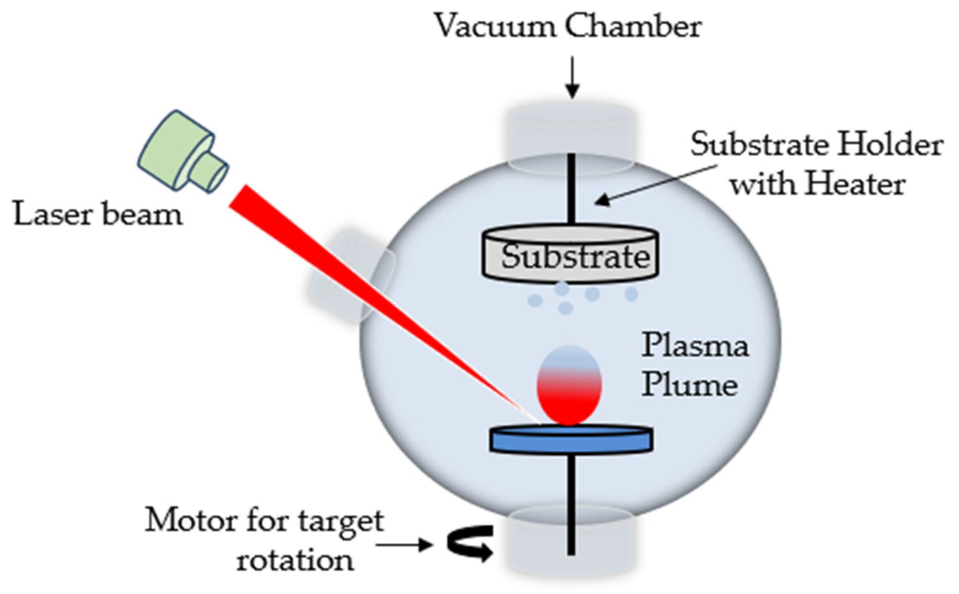
A PLD system consists of a vacuum chamber with at least one window that is transparent to the incident laser wavelength. Within the vacuum chamber, two main components must be present: the target and the substrate holder. The diameter of the target usually does not exceed 25 mm. These two components are separated by a predefined gap so that the surface of the target faces the substrate holder. A laser is used to ablate the target, creating a plasma that expands toward the substrate in the form of what is commonly referred to as a “plasma column”. This plasma corresponds to energetic substances, which are deposited on the substrate and form a thin film [18]. The area of the target ablated by the laser, commonly referred to as spot size, correlates to the number of removed species per pulse. Spot size is generally either square or rectangular, with an approximate area of a few square millimeters.
The physical process of PLD can be divided into laser–target interaction, plasma spatial evolution, and deposition of sputtered material on the substrate surface. An illustration of the pulsed laser deposition method is displayed in Figure 1. The laser–target interaction involves high-energy transient interactions between pulsed lasers with different wavelengths and pulse widths and various types of targets. This interaction is governed by physical theories including the heat conduction model, the dual-temperature model [19], and the Coulomb explosion model [20], among others. The spatial evolution of plasma is a complex kinetic process. It is particularly noteworthy that within the plasma, there exists a region layer with a thickness merely equivalent to a few gas molecules’ mean free path. When the laser ablates the target material, the particle density ejected from the target surface can reach 1016 to 1027 cm−3. In this region, close to the target surface, an extensive collision among particles of such high density occurs, leading to the rapid adjustment, redistribution, and convergence of velocities of particles with varying energies within a very short period. The existence of the Knudsen layer is the fundamental reason for the compositional fidelity of PLD, ensuring that the composition of the deposited film remains consistent with that of the target material. The plume generated by the pulsed laser is highly directional, and the density and speed of the particles in all directions in space are different; these will affect the uniformity of the film. Therefore, the PLD process for the preparation of large-area films requires further optimization of the deposition parameters. The spatial distribution of matter in the plasma typically follows; the normalized distribution function Z(θ) is defined by Equation (1):
Here, θ refers to the angle relative to the normal direction, and the value of n, which is related to the type of target material, ranges approximately from 4 to 11 [21]. The uneven spatial distribution of matter within the plasma makes the large-area uniformity of Pulsed Laser Deposition a challenge. Finally, when the sputtered material reaches the substrate surface, factors such as the properties and temperature of the substrate directly influence the adsorption, nucleation, and growth on the substrate, thus affecting the structure and morphology of the final deposited layer.
2. Halide Perovskite Materials
2.1. Structure and Property
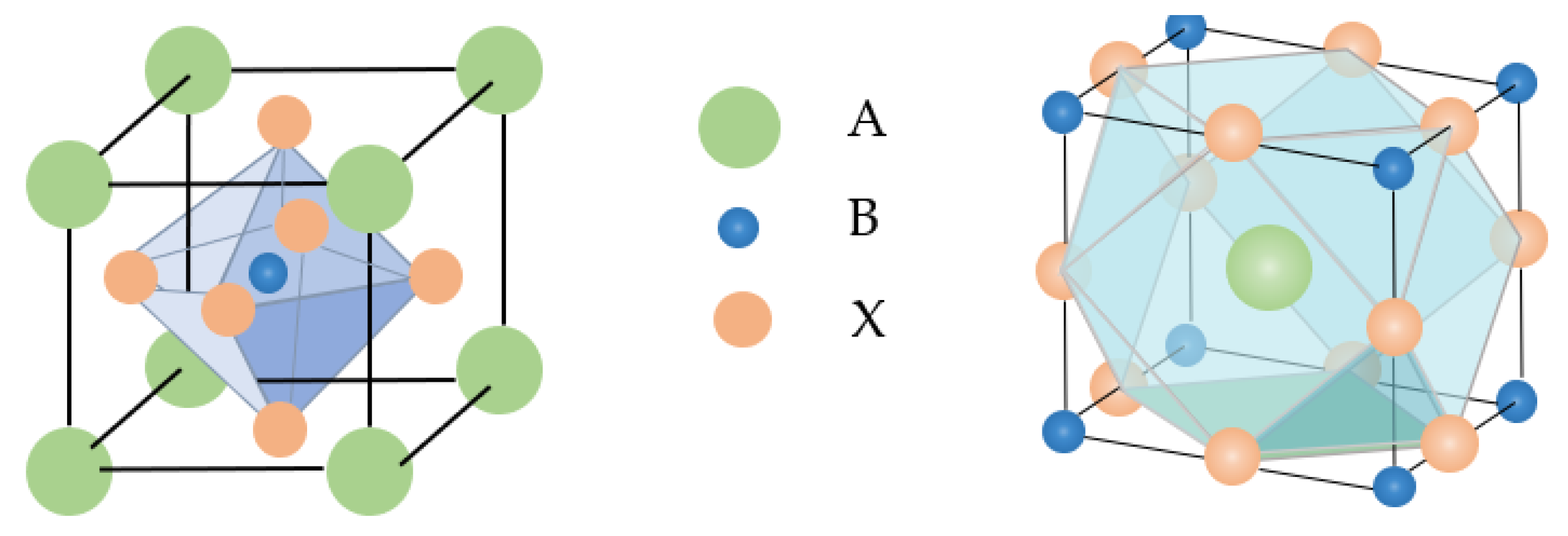
Perovskite structure materials have gained widespread attention in recent years due to their high light absorption coefficient, long carrier lifetime, low cost, simple fabrication process, and scalability [22,23,24,25]. Perovskite materials primarily refer to a category of materials composed of cations, metal cations, and halide ions, featuring a CaTiO3-type crystal structure [26] as shown in Figure 2, with the general formula ABX3. Herein, ‘A’ represents a cation, such as organic cations methylammonium (CH3NH3+, MA+) or formamidinium (HC(NH2)2+, FA+), and metal cations like cesium (Cs+) or rubidium (Rb+); ‘B’ typically denotes a divalent metal cation, such as lead ion (Pb2+) or tin ion (Sn2+); ‘X’ stands for a halide anion, including chloride (Cl−), bromide (Br−), or iodide (I−) [27]. Organic chalcogenides and inorganic perovskite materials are defined according to the classification of A cations into organic and inorganic cations, and their main representative materials are CH3NH3PbI3 and CsPbBr3, respectively. Six halide anions X− and one metal ion B2+ form an octahedron [BX6]4−, with B2+ located at the center of the octahedron [BX6]4−, and X− positioned at the vertices of the octahedron [BX6]4−. These octahedra share vertices to extend into a three-dimensional spatial structure, with A+ situated at the center formed by four octahedra. Consequently, the stability and degree of deformation of the perovskite structure can be predicted through the tolerance factor t and the octahedral factor μ [28]. These parameters, t and μ, are calculated using Equations (2) and (3), respectively.
Here, rA, rM, and rX represent the ionic radii of A+, B2+, and X− ions, respectively, in the perovskite structure. The ideal perovskite structure is characterized by a tolerance factor t that approaches unity. When the tolerance factor satisfies the condition of 0.8 ≤ t ≤ 1, the perovskite can maintain a stable cubic crystallographic structure. The octahedral factor μ can be utilized to evaluate the potential formation of a stable regular octahedral [BX6]4− structure. A stable octahedral geometry can be formed when μ satisfies the condition of 0.414 ≤ μ ≤ 0.592 [29].
Figure 2.
Crystal structure of the perovskite [30].
Figure 2.
Crystal structure of the perovskite [30].

As it is a direct bandgap semiconductor, perovskite can control spectral tuning by substitution or mixing of halide components and cations. The luminous wavelength ranges from 390 nm to 790 nm and can be extended to 820 nm by mixing methyl and formamidine [31].
2.2. Preparation of Perovskites
In order to fabricate high-performance optoelectronic devices based on perovskite thin-film structures, it is important to deposit the absorber layer controllably onto a uniformly covered thin film. It is widely believed that the performance of the devices largely relies on the fabrication methods of perovskite thin films [32,33,34,35,36]. So far, solution processing and vapour deposition methods have been extensively employed for the fabrication of perovskite thin films. Both of these methods have produced efficient solar cells and other optoelectronic devices [37]. The solution method (spin-coating) is simple, inexpensive, and is suitable for large-scale preparation of thin films. However, the quality of films prepared by spin-coating is often not as good as films prepared by PLD due to factors such as rotation speed and coating concentration. In view of the convenience of adding some additives/passivators to the solution precursor of the spin-coating method to reduce surface defects and improve the film quality, the solution spin-coating method is widely used in the laboratory for the preparation of perovskite solar cells.
2.2.1. Solution Deposition Method
In the solution deposition method, the precursors are initially mixed in a solvent under ambient conditions. The resulting thin films can be deposited using techniques such as spinning coating [38,39,40], knife coating [41], spray coating [42,43], and printing methods [44]. Solution deposition offers ease of operation and presents several advantages.
In earlier studies, perovskite thin films were primarily deposited using the one-step spin-coating method, as shown in Figure 3. Actually, thin films deposited by solution deposition often exhibit low coverage, small grain size, and high surface roughness, leading to poor device performance. In the one-step method, the precursor materials BX2 and AX are dissolved in a polar solvent such as N,N-dimethylformamide (DMF) and dimethyl sulfoxide (DMSO) in specific proportions. The mixed solvent is then deposited onto a substrate through spin-coating, allowing for rapid solvent evaporation. During the solvent evaporation process, perovskite crystallization occurs, ultimately resulting in the formation of a perovskite thin film on the substrate. Controlling the rapid crystallization of perovskite films during solvent evaporation is challenging in the one-step method. It is difficult to control the quick crystallization of perovskite films during solvent evaporation in the one-step method. Extensive pin-holes in perovskite thin films result in poor device performance and reproducibility.
Burschka et al. [32] introduced an enhanced technique, commonly known as the two-step method, as shown in Figure 3, aimed at enhancing the coverage of perovskite films. In this approach, BX2 and AX are dissolved in separate solvents. Initially, lead iodide (PbI2) is incorporated into TiO2 nanopores via spin-coating. Subsequently, the TiO2/PbI2 composite film is immersed in a solution of CH3NH3I in 2-propanol. Ultimately, a high-quality dark brown thin film of CH3NH3PbI3 is formed.
2.2.2. Vapour Deposition Method
In contrast, the vapour deposition method enables the uniform and high coverage of perovskite thin films. When compared to solution-based methods, vapour deposition results in thin films with a uniform, smooth, and dense surface, exhibiting minimal pin-holes. Consequently, this enhances the crystallinity of perovskite thin films and device performance.
The vacuum processing technology is generally divided into two major categories, physical vapour deposition (PVD) and chemical vapour deposition (CVD), including co-evaporation [47,48], sequential evaporation [49], and double-layer evaporation [50]. There are also a few methods combining the solution and vacuum processes [51].
2.3. Application in Photoelectric Devices
Over the past decades, direct band gap inorganic semiconductors have been extensively researched for their potential in high-efficiency optoelectronic devices. Meanwhile, the development of organic–inorganic hybrid perovskites has demonstrated unique properties, including strong photoluminescent quantum yields, long-range electron-hole diffusion lengths, and low nonradiative recombination rates. Consequently, perovskites have emerged as promising candidates for light-emitting devices. The rapid progress achieved in perovskite solar cells in recent years has served as an inspiration to explore the application of perovskites in other optoelectronic devices, including light-emitting diodes [52], lasers [53,54], and photodetectors [55].
3. PLD Preparation of Perovskite Solar Cells
Perovskite solar cells (PSCs) are third-generation solar cells that utilize organic–inorganic hybrid metal halide perovskite semiconductors as the absorbing material to directly convert light energy into electrical energy through the photovoltaic effect. The device structure can be mainly divided into two categories: mesoporous structures and planar structures. Planar structures can be divided into n-i-p (regular) type and p-i-n (inverted) type, as shown in Figure 4.
PSCs typically consists of six main components: transparent conductive glass, electron transport layer, mesoporous layer, perovskite layer, hole transport layer, and metal electrode. In most cases, FTO glass or ITO glass is used as the transparent conductive glass and serves as the cathode in the device. The electron transport layer is typically an n-type semiconductor material, such as SnO2, TiO2 or ZnO, which facilitates electron transport and blocks hole diffusion [57,58,59,60]. The mesoporous layer, composed of materials like TiO2 or A12O3, acts as a support framework for the perovskite layer, enhancing the contact area and improving performance. The perovskite layer consists of organic–inorganic perovskite materials, such as MAPbX3 and CsPbX3. The hole transport layer is selected as a p-type semiconductor and can be either an organic material like Spiro-OMeTAD or PTAA, or an inorganic material like NiOx [61]. Commonly used metal materials for PSC electrodes include Al, Ag, and Al, while non-metal materials such as conductive carbon are also employed.
Pulsed laser deposition (PLD) is a physical vapour deposition technique (PVD) widely used to grow oxide perovskites, which allows conformal growth of films without damaging the underlayers, making this technique highly attractive for full solar cell devices. Different from conventional solution-based processes that dissolve halide salt precursors in organic solvents like dimethylformamide (DMF) or dimethyl sulfoxide (DMSO), PLD requires a solid target containing the desired material. This target can be prepared through either wet chemistry [62] or dry mechanochemical synthesis (MCS) [63]. Unlike wet chemistry, MCS is not constrained by the incompatible solubility of halide salt precursors. However, one major challenge in the perovskite film preparation by PLD is the precise control of the stoichiometry. Due to the property of the easily vaporizable (organic) and not easily vaporizable (inorganic) components of the hybrid material, targets prepared according to the original stoichiometric ratios usually do not yield the expected thin films. Researchers have made great efforts in film preparation by varying the different deposition parameters, among others, deposition pressure, laser spot size, and substrate type. Table 1 summarizes the findings from the literature.
3.1. Hybrid Perovskite Layer
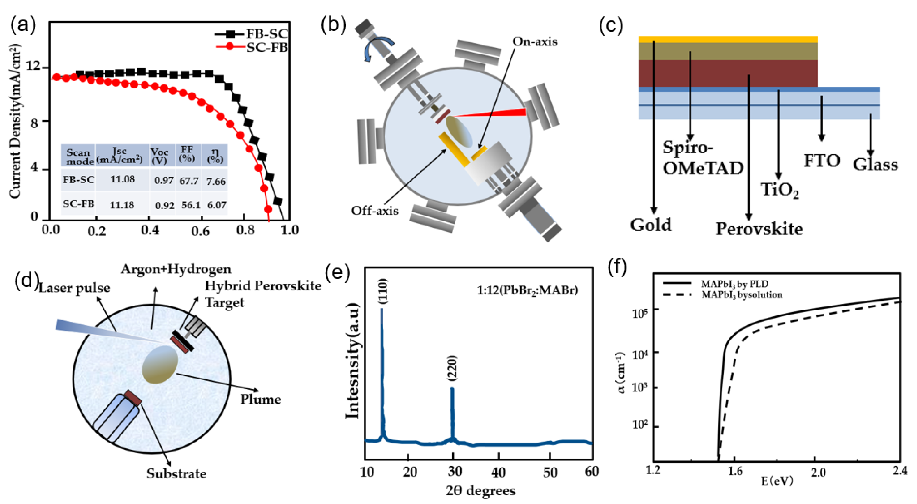
Bansode U. et al. [64] successfully prepared high-quality MAPbI3 films by off-axis pulsed laser deposition and the conversion efficiency of perovskite solar cell prepared at room temperature is about 7.7%, as shown in Figure 5a, proving the possibility of the PLD technique for achieving room-temperature growth of high-quality thin films of hybrid perovskites. Pulses of an excimer laser (λ = 248 nm; energy density: 0.3 J/cm2; pulse rep rate: 5 Hz) were made incident on the target held in a vacuum chamber held at 10−6 Torr. For a ratio of PbI2:MAI = 1:4 mol in the target, the off-axis grown film gives near-perfect stoichiometry of the perovskite phase, as shown in Figure 5b. Furthermore, Bansode U. et al. [65] used conventional on-aixs PLD to deposit MAPbBr3 thin films and prepare planar heterojunction solar cells with the highest conversion efficiency, reaching 10.9%, as shown in Figure 5c. The pulsed laser deposition was carried out using a KrF excimer laser (λ = 248 nm, energy density 0.3 J/cm2, pulse rep rate 5 Hz, and substrate temperature 100 °C, with a target-substrate distance of 5 cm). Bansode U. et al. demonstrated by increasing the inorganic–organic composition (PbBr2:MABr) in the target further to 1:12 along with the use of a mixture of argon and hydrogen (90%:10%) for momentum softening of the generated radical/ions in the forward-directed plasma plume, as shown in Figure 5d; they achieved a perfect highly oriented (110) MAPbBr3 film with good stoichiometry.
Unlike other PVD methods such as co-evaporation that requires the use of two sources to deposit MAPbI3, Tatiana Soto-Montero et al. [66] achieved single-source, single-step deposition of MA1-xFAxPbI3 thin films by pulsed laser deposition with tunable stoichiometric ratios and produced n-i-p solar cells with an efficiency of 14%, as shown in Figure 5e. Apart from common basic parameters of the deposition process (λ = 248 nm, energy density 0.3 J/cm2, pulse rep rate 5 Hz, with a target-substrate distance of 60 mm), Tatiana Soto-Montero et al. detailed the relationship between the laser spot size and instantaneous growth speed (per pulse) by changing the spot size from 1.0 to 2.5 mm2. When using 2.5 mm2 spot size, it is possible to grow 500 nm thick films of MAPbI3 in 36 min, approximately four times faster than other well-known PVD techniques. To control the deposition pressure during PLD, an inert gas (Ar) is introduced in the chamber. The main function of this gas is to reduce the kinetic energy of the particles in the plasma plume, acting as a moderator of the arriving species as well as promoting thermalization of the ablated species.
From the above research, we can find that the target stoichiometry and the deposition pressure plays a key role in controlling the film composition, microstructure, and optical properties. At high pressures, the thermalization of particles allows nearly equal transfer (smaller plasma plume size). In contrast, the scattering of light elements is more likely to occur at low pressures (fewer organic species arriving at the substrate).
3.2. Inorganic Perovskite Layer
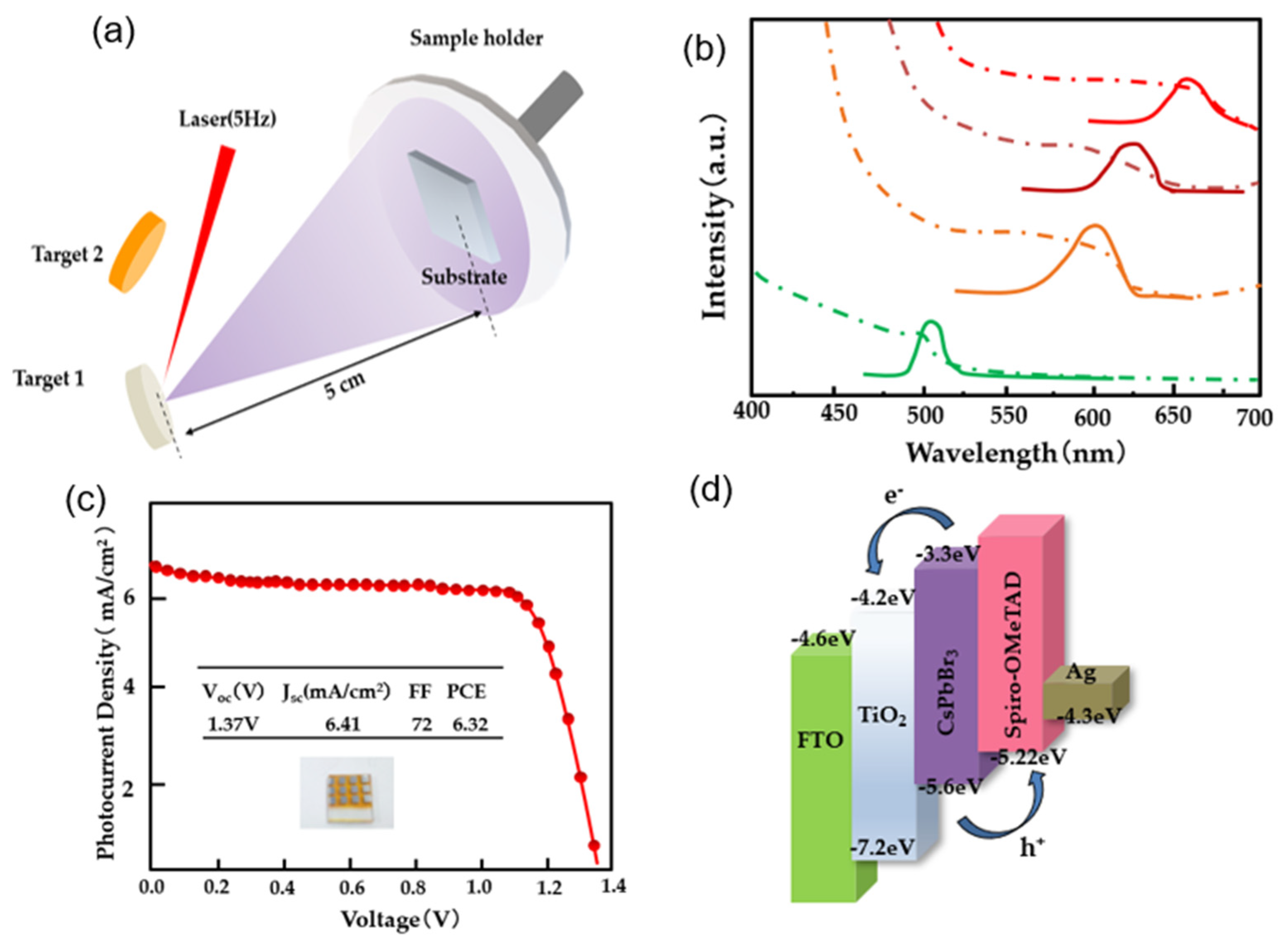
Organic–inorganic hybrid halide perovskite materials are easily degraded in humid and high-temperature environments. Therefore, cesium-based inorganic halide perovskites have been studied intensively to substitute the organic–inorganic hybrid perovskites in PSCs, which can fundamentally solve the thermal and humid instability [72,73,74]. Jin X. et al. [75] investigated the preparation of inorganic perovskite CsPbIxBr3-x (x = 0, 1, 2, 3) thin films based on a solid-phase reaction. The pulsed laser deposition was carried out using a KrF excimer laser (λ = 248 nm, energy 120 mJ, pulse rep rate 5 Hz, and substrate temperature 330 °C, with a target-substrate distance of 5 cm). The halide element ratio x (x = 0, 1, 2, 3) of CsPbIxBr3−x thin films can be changed by selecting two PLD targets, as shown in Figure 6a. Two solid-phase precursor thin films are deposited with a suitable thickness ratio and then undergo a high-temperature reaction without any by-products or gas volatilization. The emission peak positions coincide well with the absorption edges, in Figure 6b, indicating that the thin films have good monochromatism and an excellent fluorescence performance. It is worth noting that by increasing the distance between the target and substrate, Jin et al. have successfully prepared 5 cm × 5 cm large-area thin films. This provides a reference for PLD application to fabricating large-area perovskite solar cells.
Wang H. et al. [67] prepared the target from CsPbBr3 single crystal powders, which were grown by an inverse temperature crystallization (ITC) method. The CsPbBr3 thin film prepared by PLD displays good stability in a high-humidity environment. Similarly, the parameters of laser deposition (λ = 248 nm, energy 100 mJ, pulse rep rate 5 Hz, and substrate temperature of 320 °C, with a target-substrate distance of 5 cm) have minor adjustments compared with CsPbIxBr3-x (x = 0, 1, 2, 3) mentioned above. Generally, the thickness of the film deposited by PLD is determined by the number of laser pulses. As the thickness of the CsPbBr3 layer is in linear dependence on the laser pulse number, Wang H. et al. [73] have further studied the influence of CsPbBr3 film thickness on PSCs’ device performances. The perovskite solar cells (FTO/c-TiO2/m-TiO2/CsPbBr3/Spiro-OmeTAD) achieved the highest power conversion efficiency of 6.3%, as shown in Figure 6c.
Figure 6.
(a) Schematic diagram of sample preparation using PLD; (b) absorption spectral (dashed curve) and PL spectra (solid curve) [72]; (c) J−V curves of CsPbBr3-based perovskite solar cell; (d) energy-level diagram of CsPbBr3-based PSCs and charge transportation processes [73].

Compared with CsPbBr3, CsPbI3 possesses the most suitable band gap (1.73 eV) for photovoltaic device applications [76]. However, its cubic structure (black α-phase) degrades rapidly to the nonphotoactive orthorhombic phase (yellow δ-phase) with a larger band gap (3.0 eV) under ambient conditions [77,78]. Furthermore, the common chemical solution preparation techniques for CsPbI3 are still hard to obtain large areas, uniform and compact CsPbI3 thin films with fewer defects. Zhou X. et al. [79] prepared the CsPbI3 thin films with black orthorhombic phase on the surface of Si(100) by PLD employing a KrF excimer laser (λ = 248 nm, energy 250 mJ, pulse rep rate 5 Hz). The cylindrical CsPbI3 target was fabricated with uniformly mixed PbI2 and CsI powder (mole ratio, 1:1) under the mechanical pressure of 40 Mpa.
3.3. Electron Transport Layers
Electron transport layers (ETL) based on tin(IV) oxide (SnO2) are recurrently employed in perovskite solar cells (PSCs) by many deposition techniques. Pulsed laser deposition (PLD) offers a few advantages for the fabrication of such layers, such as being compatible with large scale, patternable, and allowing deposition at fast rates.
Pulsed laser deposition (PLD) has already been adopted as a low damage deposition technique of transparent conducting oxides on top of sensitive organic charge transport layers in optoelectronic devices. Zanoni K. P. S. et al. [68] used a PLD tool equipped with a droplet trap to minimize the number of excess particles reaching the substrate and obtained surfaces with very low roughness, the results are shown in Figure 7. The SnOx deposition conditions were optimized by using a constant laser fluence of 1.5−1.6 J/cm2, with a laser frequency set at 25 Hz. The substrates were kept at room temperature during the whole PLD process. The number of oxygen vacancies in the film can be affected by changing the concentration of oxygen in the background gas. Zanoni K. P. S.’s team finally obtained the solar cell in the n-i-p configuration employing methylammonium lead iodide perovskite as the absorber layer with power conversion efficiencies exceeding 18%.
Among the metal oxides reported as ETLs in planar PSCs, like SnO2, ZnO and organic compounds, TiO2 prevails in most of the highly efficient planar or mesoporous PSCs. Mazumdar, S. et al. [69] studied TiO2 films deposited on FTO substrates by PLD under various conditions and utilized as the ETL of PSCs. The best performing one is deposited at room temperature and yields in a PSC with 17% efficiency. An excimer laser with 248 nm wavelength is subjected to a TiO2 target (99.99% pure), with the energy of 42 mJ/pulse and the laser frequency set at 10 Hz. Through optimizing PLD conditions (substrate temperature, target-substrate distances), the enhanced crystallinity of the epitaxial films improves photogenerated charge transport while maintaining sufficient porosity.
3.4. Hole Transport Layers
The hydrophilism and acidity of some organic HTLs are harmful to the perovskite layer, often resulting in poor device stability, which is a major concern for PSCs. Alternatively, some inorganic semiconductors such as NiOx [70], CuSCN [80], and CuOx films are considered as suitable candidates for achieving stable HTLs for inverted PSCs. Among them, NiOx thin films have attracted particular attention as HTLs for PSCs due to their high optical transmittance, high conductivity, good chemical stability, good electron blocking capability, and good alignment of valence band maximum (VBM) with perovskite layers. Although spin-coated Cu-doped NiOx film used as HTLs for PSCs had improved the efficiency, the solution-based processes generally suffered from poor reproducibility.
Feng M. et al. [71] systematically studied the optical and electrical properties of Cu-doped NiOx films and the photovoltaic performance of PSCs with NiOx HTL. Cu-doped NiOx with different doping concentrations that varied from 0% to 5% were successfully prepared by a high-temperature solid-state reaction. To be specific, for the Cu-doped NiOx target, the Cu2O powder (mole ratio Cu/Ni = 1%, 3%, and 5%) was mixed with NiO powder for adequate grinding in mortar, then pressed under a pressure of 30 MPa for 0.5 h, and was sintered in a furnace at 900 °C for 48 h under an oxygen-rich atmosphere. The laser energy was set to 300 mJ with a 5 Hz pulse frequency, and the distance between the target and substrate was about 5 cm. The deposition was at room temperature, and oxygen partial pressure controlled at 11.0 Pa was favourable to form intrinsic p-type NiOx films under an oxygen-rich atmosphere. Furthermore, inverted planar PSCs with Ag/LiF/RhB101/PCBM/FA0.2MA0.8PbI3−xClx/NiOx (Cu:NiOx)/FTO/glass configurations were fabricated. Under the optimal conditions, PSCs with 3% Cu:NiOx films as HTLs exhibited a current density and PCE of 23.17 mA/cm2 and 20.41%, as shown in Figure 8a, which were much higher than those of the PSCs with undoped NiOx HTLs, and it is the best efficiency among the PSCs with physical vapour-deposited NiOx HTLs.
In most of the research, the PLD technique has been used to prepare only one of the transport layers of perovskite solar cells. Song, Q. et al. [70] tried to fabricate the solar cells by depositing the perovskite layer (CsPbBr3) and the hole transport layer (NiOx) in sequence in the chamber. After exploring the overall annealing temperature on the device performance, they achieved all-inorganic CsPbBr3. PSCs specifically can maintain 95% of initial efficiency for 1200 h under the condition of 85 °C and 30% relative humidity with a champion efficiency of 5.47%. So far, the maximum efficiency of CsPbBr3 PSCs has reached 11.08% [81]. There is a significant gap compared to the maximum performance fabricated by the solution method.
3.5. Surface Plasmons in PSCs
In order to enhance the efficiency of perovskite solar cells, various approaches have been developed to promote light-harvesting capabilities or to tailor carrier transport kinetics for maximized charge collection. Metallic nanoparticles (MNPs) with plasmonic properties, including Au, Ag, Al, and Cu, are widely employed in various photoelectric devices. This is attributed to their exceptional optical and near-field electromagnetic properties stemming from the localized surface plasmon resonance (LSPR) effects of MNPs [71,80,81,82,83]. The light excites the electrons at the fermi level of a plasmonic NP and raises it to the localized surface plasmon energy level. From here, the hot electrons are transferred to the conduction band of the semiconductor and increase the minority charge carriers in the semiconductor (especially, in the active layers of solar) [84,85,86]. The specific mechanisms and magnitude of plasmonic enhancement in PSCs are closely linked to the structure of PSCs. Optimal selection of MNPs enhancers alongside thoughtful design of device structures is critical for maximizing the LSPR effects in plasmonic PSCs [87,88].
Gezgin, S.Y. et al. [89] enhanced the conversion efficiency and photo current of Si/CZTS solar cells by embedding gold nanoparticles in CZTS films. Au plasmonic NPs can provide hot electron transfer to semi-conductor in which it is embedded as well as photon absorption and photon scattering. Au nanoparticles were deposited at room temperature by laser beam at energies of 26 mJ, 30 mJ, 32 mJ, and 36 mJ and it was determined that ideal laser energy to be used for Au NPs to be embedded into CZTS films, as shown in Figure 9. The characteristics and distribution of Au nanoparticles can be changed by adjusting the laser energy during the preparation process using PLD. Si/CZTS solar cells with Au NPs (by laser energy of 36 mJ) embedded into CZTS film achieved a better device performance (Jsc = 24.43 mA/cm2, Voc = 300 mV, FF = 0.16 and η = 1.45%), as shown in Figure 9.
The current mainstream approach of realizing plasmonic PSCs is solution spin-coating method. MNPs are usually added to the perovskite layer precursor solution at a certain concentration [90,91,92]. Not much research work has been carried out on PLD preparation of MNPs as well as the application in perovskite solar cells. There is still a lot of room for future research in this area.
4. Conclusions
This paper introduces the application of PLD technology in perovskite solar cells from the deposition principle and development history of pulsed laser deposition technology. After a brief introduction to the principle of perovskite solar cells, we compared two mainstream methods for preparing perovskite solar cells: the solution method and the physical meteorological deposition method. Generally, pulsed laser deposition technology can obtain high-quality films with low defects by means of very good controllability and designability of growth parameters. Targets used in PLD techniques, unlike the solution method, are not constrained by the incompatible solubility of halide salt precursors. Through summarizing recent scientific research work on the preparation of perovskite solar cells by pulsed laser deposition of the active layer, electron transport layer, and hole transport layer, we can see the advantages of pulsed laser deposition technology in obtaining high-quality thin films; of course, due to the limitations of vacuum technology, pulsed laser technology in the preparation of the PSCs’ cost is higher than the solution method. At present, the generally high-efficiency solar cells are obtained by the organic solution spin-coating method and interface engineering. For the application of PLD in perovskite solar cells, most of the research has focused on the preparation and optimization of a particular one-transport layer (ETL/perovskite layer/HTL). Results show that PLD techniques do yield higher quality films while failing to achieve the highest efficiency of PSCs. One of the reasons is that the preparation of the organic–inorganic hybrid perovskite layer by PLD requires strict parameters (target component, deposition pressure, laser spot size, etc.) so that the PLD process is not as repeatable as solution methods. What is more, common optimization strategies applied in PSCs like additive engineering and interface engineering are more suitable for solution methods, which limit the PLD technique from setting high-efficiency records. However, the application of solution methods like spin-coating is challenging for the integration into heterostructures such as monolithic tandem devices and large-area depositions. We hold a promising outlook for PLD preparing fully physical vapour-processed halide PSCs and optoelectronic devices.
Funding
This research received no external funding.
Conflicts of Interest
The authors declare no conflicts of interest.
References
- Smith, H.M.; Turner, A.F. Vacuum Deposited Thin Films Using a Ruby Laser. Appl. Opt. 1965, 4, 147–148. [Google Scholar] [CrossRef]
- Dijkkamp, D.; Venkatesan, T.; Wu, X.D.; Shaheen, S.A.; Jisrawi, N.; Min-Lee, Y.H.; McLean, W.L.; Croft, M. Preparation of Y-Ba-Cu oxide superconductor thin films using pulsed laser evaporation from high T c bulk material. Appl. Phys. Lett. 1987, 51, 619–621. [Google Scholar] [CrossRef]
- Haider, A.J.; Alawsi, T.; Haider, M.J.; Taha, B.A.; Marhoon, H.A. A comprehensive review on pulsed laser deposition technique to effective nanostructure production: Trends and challenges. Opt. Quantum Electron. 2022, 54, 488. [Google Scholar] [CrossRef]
- Duta, L.; Popescu, A.C. Current Research in Pulsed Laser Deposition. Coatings 2021, 11, 274. [Google Scholar] [CrossRef]
- Willmott, P.R.; Huber, J.R. Pulsed laser vaporization and deposition. Rev. Mod. Phys. 2000, 72, 315–328. [Google Scholar] [CrossRef]
- Wagner, G.; Lange, U.; Bente, K.; Lenzner, J.; Lorenz, M. Defect structure of monocrystalline (001)-oriented Zn0.62Cu0.19In0.19S films grown on GaP by pulsed laser deposition (PLD). J. Cryst. Growth 2000, 209, 68–74. [Google Scholar] [CrossRef]
- Mao, W.; Gong, W.; Gu, Z.; Wilde, M.; Chen, J.; Fukutani, K.; Matsuzaki, H.; Fugetsu, B.; Sakata, I.; Terai, T. Hydrogen diffusion in cerium oxide thin films fabricated by pulsed laser deposition. Int. J. Hydrogen Energy 2024, 50, 969–978. [Google Scholar] [CrossRef]
- Ullrich, B.; Brown, G. Room temperature photoluminescence of amorphous GaAs. Mater. Lett. 2009, 63, 2489–2491. [Google Scholar] [CrossRef]
- Shen, Y.; Hong, J.-I.; Xu, S.; Lin, S.; Fang, H.; Zhang, S.; Ding, Y.; Snyder, R.L.; Wang, Z.L. A General Approach for Fabricating Arc-Shaped Composite Nanowire Arrays by Pulsed Laser Deposition. Adv. Funct. Mater. 2010, 20, 703–707. [Google Scholar] [CrossRef]
- Fourmont, P.; Gerlein, L.F.; Fortier, F.-X.; Cloutier, S.G.; Nechache, R. Highly Efficient Thermoelectric Microgenerators Using Nearly Room Temperature Pulsed Laser Deposition. ACS Appl. Mater. Interfaces 2018, 10, 10194–10201. [Google Scholar] [CrossRef]
- Kobayashi, T.; Ogawa, H.; Nabeshima, F.; Maeda, A. Interface superconductivity in FeSe thin films on SrTiO3 grown by the PLD technique. Supercond. Sci. Technol. 2022, 35, 07LT01. [Google Scholar] [CrossRef]
- Bhandari, S.; Hao, B.; Waters, K.; Lee, C.H.; Idrobo, J.-C.; Zhang, D.; Pandey, R.; Yap, Y.K. Two-Dimensional Gold Quantum Dots with Tunable Bandgaps. ACS Nano 2019, 13, 4347–4353. [Google Scholar] [CrossRef] [PubMed]
- Serna, M.I.; Yoo, S.H.; Moreno, S.; Xi, Y.; Oviedo, J.P.; Choi, H.; Alshareef, H.N.; Kim, M.J.; Minary-Jolandan, M.; Quevedo-Lopez, M.A. Large-Area Deposition of MoS2 by Pulsed Laser Deposition with In Situ Thickness Control. ACS Nano 2016, 10, 6054–6061. [Google Scholar] [CrossRef]
- Zubir, N.S.M.; Zhang, H.; Zou, G.; Bai, H.; Deng, Z.; Feng, B.; Wu, A.; Liu, L.; Zhou, Y.N. Large-Area Die-Attachment Sintered by Organic-Free Ag Sintering Material at Low Temperature. J. Electron. Mater. 2019, 48, 7562–7572. [Google Scholar] [CrossRef]
- Jia, Q.; Zou, G.; Wang, W.; Ren, H.; Zhang, H.; Deng, Z.; Feng, B.; Liu, L. Sintering Mechanism of a Supersaturated Ag–Cu Nanoalloy Film for Power Electronic Packaging. ACS Appl. Mater. Interfaces 2020, 12, 16743–16752. [Google Scholar] [CrossRef]
- Juvaid, M.M.; Sarkar, S.; Gogoi, P.K.; Ghosh, S.; Annamalai, M.; Lin, Y.-C.; Prakash, S.; Goswami, S.; Li, C.; Hooda, S.; et al. Direct Growth of Wafer-Scale, Transparent, p-Type Reduced-Graphene-Oxide-like Thin Films by Pulsed Laser Deposition. ACS Nano 2020, 14, 3290–3298. [Google Scholar] [CrossRef]
- Shin, Y.J.; Kim, Y.; Kang, S.; Nahm, H.; Murugavel, P.; Kim, J.R.; Cho, M.R.; Wang, L.; Yang, S.M.; Yoon, J.; et al. Interface Control of Ferroelectricity in an SrRuO3/BaTiO3/SrRuO3 Capacitor and its Critical Thickness. Adv. Mater. 2017, 29, 1602795. [Google Scholar] [CrossRef]
- Shepelin, N.A.; Tehrani, Z.P.; Ohannessian, N.; Schneider, C.W.; Pergolesi, D.; Lippert, T. A practical guide to pulsed laser deposition. Chem. Soc. Rev. 2023, 52, 2294–2321. [Google Scholar] [CrossRef] [PubMed]
- Vatsya, S.R.; Virk, K.S. Solution of two-temperature thermal diffusion model of laser–metal interactions. J. Laser Appl. 2003, 15, 273–278. [Google Scholar] [CrossRef]
- Stoian, R.; Boyle, M.; Thoss, A.; Rosenfeld, A.; Korn, G.; Hertel, I.V.; Campbell, E.E.B. Laser ablation of dielectrics with temporally shaped femtosecond pulses. Appl. Phys. Lett. 2002, 80, 353–355. [Google Scholar] [CrossRef]
- Ojeda-G-P, A.; Schneider, C.W.; Döbeli, M.; Lippert, T.; Wokaun, A. The importance of pressure and mass ratios when depositing multi-element oxide thin films by pulsed laser deposition. Appl. Surf. Sci. 2016, 389, 126–134. [Google Scholar] [CrossRef]
- Xiang, W.; Tress, W. Review on Recent Progress of All-Inorganic Metal Halide Perovskites and Solar Cells. Adv. Mater. 2019, 31, e1902851. [Google Scholar] [CrossRef] [PubMed]
- Jacak, J.E.; Jacak, W.A. Routes for Metallization of Perovskite Solar Cells. Materials 2022, 15, 2254. [Google Scholar] [CrossRef] [PubMed]
- Laska, M.; Krzemińska, Z.; Kluczyk-Korch, K.; Schaadt, D.; Popko, E.; Jacak, W.A.; Jacak, J.E. Metallization of solar cells, exciton channel of plasmon photovoltaic effect in perovskite cells. Nano Energy 2020, 75, 104751. [Google Scholar] [CrossRef]
- Wang, H.; Liu, H.; Li, W.; Zhu, L.; Chen, H. Inorganic perovskite solar cells based on carbon electrodes. Nano Energy 2020, 77, 105160. [Google Scholar] [CrossRef]
- Chen, Y.; Li, F.; Zhang, M.; Yang, Z. Recent Progress on Boosting the Perovskite Film Quality of All-Inorganic Perovskite Solar Cells. Coatings 2023, 13, 281. [Google Scholar] [CrossRef]
- Chakrabartty, J.; Harnagea, C.; Celikin, M.; Rosei, F.; Nechache, R. Improved photovoltaic performance from inorganic perovskite oxide thin films with mixed crystal phases. Nat. Photonics 2018, 12, 271–276. [Google Scholar] [CrossRef]
- Bartel, C.J.; Sutton, C.; Goldsmith, B.R.; Ouyang, R.; Musgrave, C.B.; Ghiringhelli, L.M.; Scheffler, M. New tolerance factor to predict the stability of perovskite oxides and halides. Sci. Adv. 2019, 5, eaav0693. [Google Scholar] [CrossRef]
- Kim, H.-S.; Seo, J.-Y.; Park, N.-G. Material and Device Stability in Perovskite Solar Cells. ChemSusChem 2016, 9, 2528–2540. [Google Scholar] [CrossRef]
- Kim, H.-S.; Im, S.H.; Park, N.-G. Organolead Halide Perovskite: New Horizons in Solar Cell Research. J. Phys. Chem. C 2014, 118, 5615–5625. [Google Scholar] [CrossRef]
- Alzahrani, H.S.; Al-Sulami, A.I.; Alsulami, Q.A.; Rajeh, A. A systematic study of structural, conductivity, linear, and nonlinear optical properties of PEO/PVA-MWCNTs/ZnO nanocomposites films for optoelectronic applications. Opt. Mater. 2022, 133, 112900. [Google Scholar] [CrossRef]
- Burschka, J.; Pellet, N.; Moon, S.-J.; Humphry-Baker, R.; Gao, P.; Nazeeruddin, M.K.; Grätzel, M. Sequential deposition as a route to high-performance perovskite-sensitized solar cells. Nature 2013, 499, 316–319. [Google Scholar] [CrossRef] [PubMed]
- Bi, D.; Moon, S.-J.; Häggman, L.; Boschloo, G.; Yang, L.; Johansson, E.M.J.; Nazeeruddin, M.K.; Grätzel, M.; Hagfeldt, A. Using a two-step deposition technique to prepare perovskite (CH3NH3PbI3) for thin film solar cells based on ZrO2 and TiO2 mesostructures. RSC Adv. 2013, 3, 18762–18766. [Google Scholar] [CrossRef]
- Basiricò, L.; Senanayak, S.P.; Ciavatti, A.; Abdi-Jalebi, M.; Fraboni, B.; Sirringhaus, H. Detection of X-Rays by Solution-Processed Cesium-Containing Mixed Triple Cation Perovskite Thin Films. Adv. Funct. Mater. 2019, 29, 1902346. [Google Scholar] [CrossRef]
- Pandey, S.; Ko, J.; Park, B.; Byun, J.; Lee, M.-J. Single crystal Perovskite-Based solar Cells: Growth, Challenges, and potential strategies. Chem. Eng. J. 2023, 466, 143019. [Google Scholar] [CrossRef]
- Zhang, H.; Tao, M.; Gao, B.; Chen, W.; Li, Q.; Xu, Q.; Dong, S. Preparation of CH3NH3PbI3 thin films with tens of micrometer scale at high temperature. Sci. Rep. 2017, 7, 8458. [Google Scholar] [CrossRef]
- Sun, J.; Wu, J.; Tong, X.; Lin, F.; Wang, Y.; Wang, Z.M. Organic/Inorganic Metal Halide Perovskite Optoelectronic Devices beyond Solar Cells. Adv. Sci. 2018, 5, 1700780. [Google Scholar] [CrossRef]
- Abbas, Z.; Azam, S.; Bashir, A.I.; Marriam, A.; Waqas, M.; Alshahrani, T.; Haq, B.U. A systematic study on optoelectronic properties of Mn4+-activated Zr-based hexafluoride red phosphors X2ZrF6 (X = K, Na, Cs): First-principles investigation and prospects for warm-white LEDs applications. Phys. Scr. 2020, 96, 015801. [Google Scholar] [CrossRef]
- Tian, J.; Wang, J.; Xue, Q.; Niu, T.; Yan, L.; Zhu, Z.; Li, N.; Brabec, C.J.; Yip, H.-L.; Cao, Y. Composition Engineering of All-Inorganic Perovskite Film for Efficient and Operationally Stable Solar Cells. Adv. Funct. Mater. 2020, 30, 2001764. [Google Scholar] [CrossRef]
- Zhang, H.; Wang, Y.; Wang, H.; Ma, M.; Dong, S.; Xu, Q. Influence of drying temperature on morphology of MAPbI3 thin films and the performance of solar cells. J. Alloys Compd. 2019, 773, 511–518. [Google Scholar] [CrossRef]
- Wu, W.-Q.; Yang, Z.; Rudd, P.N.; Shao, Y.; Dai, X.; Wei, H.; Zhao, J.; Fang, Y.; Wang, Q.; Liu, Y.; et al. Bilateral alkylamine for suppressing charge recombination and improving stability in blade-coated perovskite solar cells. Sci. Adv. 2019, 5, eaav8925. [Google Scholar] [CrossRef] [PubMed]
- Zhao, Y.; Ma, F.; Gao, F.; Yin, Z.; Zhang, X.; You, J. Research progress in large-area perovskite solar cells. Photonics Res. 2020, 8, A1–A15. [Google Scholar] [CrossRef]
- Zhang, Z.; Ba, Y.; Chen, D.; Ma, J.; Zhu, W.; Xi, H.; Chen, D.; Zhang, J.; Zhang, C.; Hao, Y. Generic water-based spray-assisted growth for scalable high-efficiency carbon-electrode all-inorganic perovskite solar cells. iScience 2021, 24, 103365. [Google Scholar] [CrossRef] [PubMed]
- Liang, C.; Li, P.; Gu, H.; Zhang, Y.; Li, F.; Song, Y.; Shao, G.; Mathews, N.; Xing, G. One-Step Inkjet Printed Perovskite in Air for Efficient Light Harvesting (Solar RRL 2/2018). Sol. RRL 2018, 2, 1770150. [Google Scholar] [CrossRef]
- Im, J.-H.; Kim, H.-S.; Park, N.-G. Morphology-photovoltaic property correlation in perovskite solar cells: One-step versus two-step deposition of CH3NH3PbI3. APL Mater. 2014, 2, 081510. [Google Scholar] [CrossRef]
- Tai, Q.; Tang, K.-C.; Yan, F. Recent progress of inorganic perovskite solar cells. Energy Environ. Sci. 2019, 12, 2375–2405. [Google Scholar] [CrossRef]
- Khazaee, M.; Sardashti, K.; Sun, J.-P.; Zhou, H.; Clegg, C.; Hill, I.G.; Jones, J.L.; Lupascu, D.C.; Mitzi, D.B. A Versatile Thin-Film Deposition Method for Multidimensional Semiconducting Bismuth Halides. Chem. Mater. 2018, 30, 3538–3544. [Google Scholar] [CrossRef]
- Becker, P.; Márquez, J.A.; Just, J.; Al-Ashouri, A.; Hages, C.; Hempel, H.; Jošt, M.; Albrecht, S.; Frahm, R.; Unold, T. Low Temperature Synthesis of Stable γ-CsPbI3 Perovskite Layers for Solar Cells Obtained by High Throughput Experimentation. Adv. Energy Mater. 2019, 9, 1900555. [Google Scholar] [CrossRef]
- Liu, X.; Tan, X.; Liu, Z.; Sun, B.; Li, J.; Xi, S.; Shi, T.; Liao, G. Sequentially vacuum evaporated high-quality CsPbBr3 films for efficient carbon-based planar heterojunction perovskite solar cells. J. Power Sources 2019, 443, 227269. [Google Scholar] [CrossRef]
- Shahiduzzaman, M.; Yonezawa, K.; Yamamoto, K.; Ripolles, T.S.; Karakawa, M.; Kuwabara, T.; Takahashi, K.; Hayase, S.; Taima, T. Improved Reproducibility and Intercalation Control of Efficient Planar Inorganic Perovskite Solar Cells by Simple Alternate Vacuum Deposition of PbI2 and CsI. ACS Omega 2017, 2, 4464–4469. [Google Scholar] [CrossRef]
- Zhang, H.; Xiang, W.; Zuo, X.; Gu, X.; Zhang, S.; Du, Y.; Wang, Z.; Liu, Y.; Wu, H.; Wang, P.; et al. Fluorine-Containing Passivation Layer via Surface Chelation for Inorganic Perovskite Solar Cells. Angew. Chem. Int. Ed. 2023, 62, e202216634. [Google Scholar] [CrossRef] [PubMed]
- Wang, S.; Wang, J.; Lou, Y.; Zhou, Y.; Wang, Z. Environment-Friendly Perovskite Light-Emitting Diodes: Progress and Perspective. Adv. Mater. Interfaces 2022, 9, 2200772. [Google Scholar] [CrossRef]
- Zhang, N.; Na, Q.; Xie, Q.; Jia, S. Development of Solution-Processed Perovskite Semiconductors Lasers. Crystals 2022, 12, 1274. [Google Scholar] [CrossRef]
- Tian, J.; Tan, Q.Y.; Wang, Y.; Yang, Y.; Yuan, G.; Adamo, G.; Soci, C. Perovskite quantum dot one-dimensional topological laser. Nat. Commun. 2023, 14, 1433. [Google Scholar] [CrossRef] [PubMed]
- Lin, C.-F.; Huang, K.-W.; Chen, Y.-T.; Hsueh, S.-L.; Li, M.-H.; Chen, P. Perovskite-Based X-ray Detectors. Nanomaterials 2023, 13, 2024. [Google Scholar] [CrossRef] [PubMed]
- Cheng, J.; Fan, Z.; Dong, J. Research Progress of Green Solvent in CsPbBr3 Perovskite Solar Cells. Nanomaterials 2023, 13, 991. [Google Scholar] [CrossRef] [PubMed]
- Li, Z.; Wang, Z.; Jia, C.; Wan, Z.; Zhi, C.; Li, C.; Zhang, M.; Zhang, C.; Li, Z. Annealing free tin oxide electron transport layers for flexible perovskite solar cells. Nano Energy 2022, 94, 106919. [Google Scholar] [CrossRef]
- Wang, Z.; Zhu, X.; Feng, J.; Wang, C.; Zhang, C.; Ren, X.; Priya, S.; Liu, S.; Yang, D. Antisolvent- and Annealing-Free Deposition for Highly Stable Efficient Perovskite Solar Cells via Modified ZnO. Adv. Sci. 2021, 8, 2002860. [Google Scholar] [CrossRef] [PubMed]
- Zhang, T.; He, Q.; Yu, J.; Chen, A.; Zhang, Z.; Pan, J. Recent progress in improving strategies of inorganic electron transport layers for perovskite solar cells. Nano Energy 2022, 104, 107918. [Google Scholar] [CrossRef]
- Zhang, H.; Wang, H.; Ma, M.; Wu, Y.; Dong, S.; Xu, Q. Application of Compact TiO2 Layer Fabricated by Pulsed Laser Deposition in Organometal Trihalide Perovskite Solar Cells. Sol. RRL 2018, 2, 1800097. [Google Scholar] [CrossRef]
- Singh, R.; Singh, P.K.; Bhattacharya, B.; Rhee, H.-W. Review of current progress in inorganic hole-transport materials for perovskite solar cells. Appl. Mater. Today 2018, 14, 175–200. [Google Scholar] [CrossRef]
- Leupold, N.; Panzer, F. Recent Advances and Perspectives on Powder-Based Halide Perovskite Film Processing. Adv. Funct. Mater. 2021, 31, 2007350. [Google Scholar] [CrossRef]
- Hong, Z.; Tan, D.; John, R.A.; Tay, Y.K.E.; Ho, Y.K.T.; Zhao, X.; Sum, T.C.; Mathews, N.; García, F.; Soo, H.S. Completely Solvent-free Protocols to Access Phase-Pure, Metastable Metal Halide Perovskites and Functional Photodetectors from the Precursor Salts. iScience 2019, 16, 312–325. [Google Scholar] [CrossRef] [PubMed]
- Bansode, U.; Naphade, R.; Game, O.; Agarkar, S.; Ogale, S. Hybrid Perovskite Films by a New Variant of Pulsed Excimer Laser Deposition: A Room-Temperature Dry Process. J. Phys. Chem. C 2015, 119, 9177–9185. [Google Scholar] [CrossRef]
- Bansode, U.; Ogale, S. On-axis pulsed laser deposition of hybrid perovskite films for solar cell and broadband photo-sensor applications. J. Appl. Phys. 2017, 121, 133107. [Google Scholar] [CrossRef]
- Soto-Montero, T.; Kralj, S.; Soltanpoor, W.; Solomon, J.S.; Gómez, J.S.; Zanoni, K.P.S.; Paliwal, A.; Bolink, H.J.; Baeumer, C.; Kentgens, A.P.M.; et al. Single-Source Vapor-Deposition of MA1–xFAxPbI3 Perovskite Absorbers for Solar Cells. Adv. Funct. Mater. 2023. [Google Scholar] [CrossRef]
- Wang, H.; Wu, Y.; Ma, M.; Dong, S.; Li, Q.; Du, J.; Zhang, H.; Xu, Q. Pulsed Laser Deposition of CsPbBr3 Films for Application in Perovskite Solar Cells. ACS Appl. Energy Mater. 2019, 2, 2305–2312. [Google Scholar] [CrossRef]
- Zanoni, K.P.S.; Pérez-Del-Rey, D.; Dreessen, C.; Rodkey, N.; Sessolo, M.; Soltanpoor, W.; Morales-Masis, M.; Bolink, H.J. Tin(IV) Oxide Electron Transport Layer via Industrial-Scale Pulsed Laser Deposition for Planar Perovskite Solar Cells. ACS Appl. Mater. Interfaces 2023, 15, 32621–32628. [Google Scholar] [CrossRef] [PubMed]
- Mazumdar, S.; Du, B.K.; Huang, C.; Lin, P.; Zhao, J.L.; Zeng, X.R.; Ke, S.M. Designing electron transporting layer for efficient perovskite solar cell by deliberating over nano-electrical conductivity. Sol. Energy Mater. Sol. Cells 2019, 200, 109995. [Google Scholar] [CrossRef]
- Song, Q.; Zhang, H.; Jin, X.; Wang, H.; Wang, P.; Ijaz, M.; Xu, Q. Highly stable all-inorganic CsPbBr3 perovskite solar cells based on pulsed laser deposition. Appl. Phys. Lett. 2023, 123, 092103. [Google Scholar] [CrossRef]
- Feng, M.; Wang, M.; Zhou, H.; Li, W.; Wang, S.; Zang, Z.; Chen, S. High-Efficiency and Stable Inverted Planar Perovskite Solar Cells with Pulsed Laser Deposited Cu-Doped NiOx Hole-Transport Layers. ACS Appl. Mater. Interfaces 2020, 12, 50684–50691. [Google Scholar] [CrossRef] [PubMed]
- Liang, J.; Zhao, P.; Wang, C.; Wang, Y.; Hu, Y.; Zhu, G.; Ma, L.; Liu, J.; Jin, Z. CsPb0.9Sn0.1IBr2 Based All-Inorganic Perovskite Solar Cells with Exceptional Efficiency and Stability. J. Am. Chem. Soc. 2017, 139, 14009–14012. [Google Scholar] [CrossRef] [PubMed]
- Guo, Q.; Duan, J.; Zhang, J.; Zhang, Q.; Duan, Y.; Yang, X.; He, B.; Zhao, Y.; Tang, Q. Universal Dynamic Liquid Interface for Healing Perovskite Solar Cells. Adv. Mater. 2022, 34, e2202301. [Google Scholar] [CrossRef] [PubMed]
- Liang, J.; Wang, C.; Wang, Y.; Xu, Z.; Lu, Z.; Ma, Y.; Zhu, H.; Hu, Y.; Xiao, C.; Yi, X.; et al. All-Inorganic Perovskite Solar Cells. J. Am. Chem. Soc. 2016, 138, 15829–15832. [Google Scholar] [CrossRef] [PubMed]
- Jin, X.; Song, S.; Liu, Z.; Wang, H.; Wang, B.; Guan, J.; Zhang, H.; Xu, Q. High-Stability Patterned CsPbIxBr3−x Thin Films with Tunable Crystal Size Prepared by Solid-Phase Reaction. Adv. Opt. Mater. 2021, 9, 2101175. [Google Scholar] [CrossRef]
- Zhao, H.; Xu, J.; Zhou, S.; Li, Z.; Zhang, B.; Xia, X.; Liu, X.; Dai, S.; Yao, J. Preparation of Tortuous 3D γ-CsPbI3 Films at Low Temperature by CaI2 as Dopant for Highly Efficient Perovskite Solar Cells. Adv. Funct. Mater. 2019, 29, 1808986. [Google Scholar] [CrossRef]
- Li, Z.; Zhou, F.; Wang, Q.; Ding, L.; Jin, Z. Approaches for thermodynamically stabilized CsPbI3 solar cells. Nano Energy 2020, 71, 104634. [Google Scholar] [CrossRef]
- Meng, L.; Wei, Z.; Zuo, T.; Gao, P. Finding junction partners for CsPbI3 in a two-terminal tandem solar cell: A theoretical prospect. Nano Energy 2020, 75, 104866. [Google Scholar] [CrossRef]
- Zhou, X.; Zhang, L.; Yan, R.; Zhang, J.; Zhou, F.; Li, X.; Wang, C.; Wang, H.; Wang, X.; Zhang, D.; et al. Fabrication and characterization of the red photodetector based on CsPbI3/n-Si heterojunction. Opt. Mater. 2021, 111, 110731. [Google Scholar] [CrossRef]
- Arora, N.; Dar, M.I.; Hinderhofer, A.; Pellet, N.; Schreiber, F.; Zakeeruddin, S.M.; Grätzel, M. Perovskite solar cells with CuSCN hole extraction layers yield stabilized efficiencies greater than 20%. Science 2017, 358, 768–771. [Google Scholar] [CrossRef]
- Zhou, Q.; Duan, J.; Du, J.; Guo, Q.; Zhang, Q.; Yang, X.; Duan, Y.; Tang, Q. Tailored Lattice “Tape” to Confine Tensile Interface for 11.08%-Efficiency All-Inorganic CsPbBr3 Perovskite Solar Cell with an Ultrahigh Voltage of 1.702 V. Adv. Sci. 2021, 8, 2101418. [Google Scholar] [CrossRef] [PubMed]
- Zhang, H.; Ijaz, M.; Blaikie, R.J. Recent review of surface plasmons and plasmonic hot electron effects in metallic nanostructures. Front. Phys. 2023, 18, 63602. [Google Scholar] [CrossRef]
- Li, P.; Jiang, X.; Huang, S.; Liu, Y.; Fu, N. Plasmonic perovskite solar cells: An overview from metal particle structure to device design. Surf. Interfaces 2021, 25, 101287. [Google Scholar] [CrossRef]
- Ijaz, M.; Zhang, H.; Chan, S.V.; Holt, R.; Davis, N.J.L.K.; Blaikie, R.J. Plasmonically coupled semiconductor quantum dots for efficient hydrogen photoelectrocatalysis. Appl. Phys. Lett. 2023, 123, 053901. [Google Scholar] [CrossRef]
- Qiu, C.; Zhang, H.; Tian, C.; Jin, X.; Song, Q.; Xu, L.; Ijaz, M.; Blaikie, R.J.; Xu, Q. Breaking bandgap limitation: Improved photosensitization in plasmonic-based CsPbBr3 photodetectors via hot-electron injection. Appl. Phys. Lett. 2023, 122, 243502. [Google Scholar] [CrossRef]
- Ijaz, M.; Zhang, H.; Xu, L.; Blaikie, R.J. Angle-resolved and time-resolved spectroscopic study on large-area silver gratings fabricated via optical interference lithography. Appl. Phys. Lett. 2023, 123, 041107. [Google Scholar] [CrossRef]
- Zhang, H.; Liu, F.; Blaikie, R.J.; Ding, B.; Qiu, M. Bifacial omnidirectional and band-tunable light absorption in free-standing core–shell resonators. Appl. Phys. Lett. 2022, 120, 181110. [Google Scholar] [CrossRef]
- Mohammadi, M.H.; Eskandari, M.; Fathi, D. Effects of the location and size of plasmonic nanoparticles (Ag and Au) in improving the optical absorption and efficiency of perovskite solar cells. J. Alloys Compd. 2021, 877, 160177. [Google Scholar] [CrossRef]
- Gezgin, S.Y.; Kılıç, H. An improvement on the conversion efficiency of Si/CZTS solar cells by LSPR effect of embedded plasmonic Au nanoparticles. Opt. Mater. 2020, 101, 109760. [Google Scholar] [CrossRef]
- Zhang, W.; Saliba, M.; Stranks, S.D.; Sun, Y.; Shi, X.; Wiesner, U.; Snaith, H.J. Enhancement of Perovskite-Based Solar Cells Employing Core–Shell Metal Nanoparticles. Nano Lett. 2013, 13, 4505–4510. [Google Scholar] [CrossRef]
- Alkhalayfeh, M.A.; Aziz, A.A.; Pakhuruddin, M.Z.; Katubi, K.M.M. Recent Advances of Perovskite Solar Cells Embedded with Plasmonic Nanoparticles. Phys. Status Solidi (a) 2021, 218, 2100310. [Google Scholar] [CrossRef]
- He, Z.; Zhang, C.; Meng, R.; Luo, X.; Chen, M.; Lu, H.; Yang, Y. Influence of Ag@SiO2 with Different Shell Thickness on Pho-toelectric Properties of Hole-Conductor-Free Perovskite Solar Cells. Nanomaterials 2020, 10, 2364. [Google Scholar] [CrossRef] [PubMed]
Figure 1.
A schematic diagram presenting the fundamental mechanism of PLD [3].
Figure 1.
A schematic diagram presenting the fundamental mechanism of PLD [3].

Figure 3.
Schematic diagram of perovskite thin films deposition methods: (Left) the solution processing methods with one-step coating method and two-step coating method [45]; (Right) the vacuum vapour method [46].

Figure 4.
The device structure of PSCs [56].
Figure 4.
The device structure of PSCs [56].

Figure 5.
(a) J-V curve for perovskite solar cell with forward and reverse scans; (b) schematic presentation and photograph of substrate arrangement for “on-axis” and “off-axis” deposition by pulsed laser deposition (PLD) [64]; (c) schematic diagram of the solar cell architecture; (d) schematic diagram of the pulsed laser deposition configuration and the process [65]; (e) X-ray diffraction (XRD) patterns of hybrid perovskites films; (f) optical properties of the optimized PLD-grown MAPbI3 films [66].

Figure 7.
(a) Schematics of the PLD system equipped with a droplet [68]; (b) schematic of the pulsed laser deposition (PLD); (c) current density-voltage (J-V) characteristics of planar perovskite photovoltaic cells assembled with PLD-grown TiO2 films on FTO substrates as electron transporting layer (ETL) [69].

Figure 8.
(a) J−V curves for PSCs with Cu:NiOx HTLs; (b) energy level diagram of various functional layers in the inverted PSCs [71].
Figure 8.
(a) J−V curves for PSCs with Cu:NiOx HTLs; (b) energy level diagram of various functional layers in the inverted PSCs [71].

Figure 9.
(left) Absorption spectra of Au NPs by laser beam at 26 mJ, 30 mJ, 32 mJ, and 36 mJ energies. (right) J-V characteristics of Au/Si/CZTS/Ag and Au/Si/plasmonic-CZTS/Ag solar cells [89].
Figure 9.
(left) Absorption spectra of Au NPs by laser beam at 26 mJ, 30 mJ, 32 mJ, and 36 mJ energies. (right) J-V characteristics of Au/Si/CZTS/Ag and Au/Si/plasmonic-CZTS/Ag solar cells [89].


Table 1.
Summary of the device structure and photovoltaic parameters of PLD-PSCs.
| Device Structure | Voc (V) | Jsc (mA·cm−2) | FF | PCE (%) | Ref. |
|---|---|---|---|---|---|
| ITO/ZnO/PLD-MAPbI3−xClx/spiro-OMeTAD/Au | 0.97 | 11.08 | 67.7 | 7.66 | [64] |
| FTO/TiO2/PLD-MAPbBr3/spiro-OMeTAD/Au | 0.98 | 20.13 | 54 | 10.9 | [65] |
| ITO/SnO2/PCBM/PLD-MA0.55FA0.45PbI3/spiro-OMeTAD/Au | 1.0 | 19.9 | 70.5 | 14.0 | [66] |
| FTO/c-TiO2/m-TiO2/PLD-CsPbBr3/spiro-OMeTAD/Ag | 1.37 | 6.41 | 72 | 6.32 | [67] |
| ITO/PLD-SnOx/C60/MAPbI3/TaTm/TPBi/MoO3/Ag | 1.11 | 21.4 | 77 | 18.1 | [68] |
| FTO/PLD-TiO2/FA0.75MA0.25PbI2.5Br0.5/spiro-OMeTAD/Au | 1.08 | 21.8 | 72 | 17 | [69] |
| FTO/PLD-c-TiO2/m-TiO2/MAPbI3/spiro-OMeTAD/Ag | 1.0 | 21.83 | 63.98 | 13.95 | [60] |
| FTO/c-TiO2/m-TiO2/PLD-CsPbBr3/PLD-NiOx/Ag | 1.38 | 6.70 | 59.24 | 5.47 | [70] |
| FTO/PLD-NiOx/FA0.2MA0.8PbI3−xClx/PCBM/RhB101/LiF/Ag | 1.11 | 23.17 | 79.1 | 20.41 | [71] |
Disclaimer/Publisher’s Note: The statements, opinions and data contained in all publications are solely those of the individual author(s) and contributor(s) and not of MDPI and/or the editor(s). MDPI and/or the editor(s) disclaim responsibility for any injury to people or property resulting from any ideas, methods, instructions or products referred to in the content. |
© 2024 by the authors. Licensee MDPI, Basel, Switzerland. This article is an open access article distributed under the terms and conditions of the Creative Commons Attribution (CC BY) license (https://creativecommons.org/licenses/by/4.0/).
Share and Cite
MDPI and ACS Style
Lu, X.; Fan, X.; Zhang, H.; Xu, Q.; Ijaz, M. Review on Preparation of Perovskite Solar Cells by Pulsed Laser Deposition. Inorganics 2024, 12, 128. https://doi.org/10.3390/inorganics12050128
AMA Style
Lu X, Fan X, Zhang H, Xu Q, Ijaz M. Review on Preparation of Perovskite Solar Cells by Pulsed Laser Deposition. Inorganics. 2024; 12(5):128. https://doi.org/10.3390/inorganics12050128
Chicago/Turabian StyleLu, Xinyu, Xingjian Fan, Hao Zhang, Qingyu Xu, and Mohsin Ijaz. 2024. "Review on Preparation of Perovskite Solar Cells by Pulsed Laser Deposition" Inorganics 12, no. 5: 128. https://doi.org/10.3390/inorganics12050128
Note that from the first issue of 2016, this journal uses article numbers instead of page numbers. See further details here.