Dataset for SERS Plasmonic Array: Width, Spacing, and Thin Film Oxide Thickness Optimization
by

Christopher M. Klenke
1,2, 
Zachary T. Brawley
1,3,
Stephen J. Bauman
1,
Ahmad A. Darweesh
1,4,
Desalegn T. Debu
3 and
Joseph B. Herzog
1,3,5,* 1
Microelectronics-Photonics Graduate Program, University of Arkansas, 731 W. Dickson St., Fayetteville, Arkansas, AR 72701, USA
2
Physics, Astronomy, and Materials Science Department, Missouri State University, 921 S. John Q Hammons Pkwy, Springfield, MO 65897, USA
3
Department of Physics, University of Arkansas, 825 W. Dickson St., Fayetteville, Arkansas, AR 72701, USA
4
Department of Physics, College of Science, AL-Nahrain University, Baghdad 10081, Iraq
5
R.B. Annis School of Engineering, University of Indianapolis, Indianapolis, IN 46227, USA
*
Author to whom correspondence should be addressed.
Data 2018, 3(3), 37; https://doi.org/10.3390/data3030037
Submission received: 22 August 2018
/
Revised: 7 September 2018
/
Accepted: 18 September 2018
/
Published: 19 September 2018
Abstract
:Surface-enhanced Raman spectroscopy (SERS) improves the scope and power of Raman spectroscopy by taking advantage of plasmonic nanostructures, which have the potential to enhance Raman signal strength by several orders of magnitude, which can allow for the detection of analyte molecules. The dataset presented provides results of a computational study that used a finite element method (FEM) to model gold nanowires on a silicon dioxide substrate. The survey calculated the surface average of optical surface enhancement due to plasmonic effects across the entire model and studied various geometric parameters regarding the width of the nanowires, spacing between the nanowires, and thickness of the silicon dioxide substrate. From this data, enhancement values were found to have a periodicity due to the thickness of the silicon dioxide. Additionally, strong plasmonic enhancement for smaller distances between nanowires were found, as expected; however, additional surface enhancement at greater gap distances were observed, which were not anticipated, possibly due to resonance with periodic dimensions and the frequency of the light. This data presentation will benefit future SERS studies by probing further into the computational and mathematical material presented previously.
Dataset: Available online: https://osf.io/6vb2w/?view_only=7629f06f081541968dbe986951167c4e
Dataset License: CC-BY-4.0
Keywords:
plasmonics; thin film; SERS; computational electromagnetics; nanowires; nano-optics; grating; array1. Introduction
Due to advances in nanotechnology engineering and manufacturing in recent years, there has been an increase in improvements to surfaced-enhanced Raman spectroscopy (SERS). SERS is important for both its versatility and effectiveness at fingerprinting analyte species. It can detect analyte molecules down to the individual molecule level [1,2,3] as well as analyze different material phases [4,5] in a variety of fields such as experimental chemical sensing (both organic and inorganic) [4], biomedical technologies [4,5], and substance detection [6,7,8] based on detecting the vibrational modes of analyte molecules. A Raman (inelastic) scattering signal forms a unique spectrum corresponding to energy shifts in the molecule compared to the Rayleigh (elastic) scattering. Unfortunately, this method is limited by the amount of light scattered in this way by molecules, which often produces a weak signal that can be difficult to detect.
To improve the limit of detection, the method of SERS can be employed. Plasmonic structures on the substrate surface can improve the Raman signal by many orders of magnitude [9,10,11] and can be tuned by taking advantage of specific nanostructure geometries capable of enhancing the electric near-field surrounding the nanostructures. One example of such nanostructures is a plasmonic nanograting; a structure that assumes a periodic assembly of plasmonic elements with nanoscale dimensions in at least one direction. By changing the space between the elements, one can create a resonance condition and maximize the local electric field enhancement, which is typically considered as the ratio of the magnitudes of the local electric field and the incident light │E/E0│ [12,13].
Computational electromagnetic methods are often used to study theoretical SERS responses of different nanostructures, making use of techniques such as finite-difference time domain (FDTD), finite element method (FEM), and discrete dipole approximation (DDA) [14,15,16]. Prior studies have primarily investigated the nanogaps between the structures and not the complete surface of the gratings [17,18]. This gap-field-only method presents an idealized data set that only accounts for light through the strongest of enhanced electrical fields and does not give a full representation of enhancement across the entire grating pattern. For practical purposes, the nanograting must improve optical enhancement not only in the space between nanowires, but across the whole surface. The data discussed in [19] and provided fully in this paper (see supplemental file) offers a more complete evaluation of the enhanced field along a substrate’s surface and its efficacy in SERS.
The data presented and discussed in this paper show the results of computational modeling of plasmonic nanostructures. A FEM was used in this study, and line averages across the surface of a simulated 2D cross-section of a grating and substrate were analyzed to improve the understanding of the electric field properties surrounding the structure.
2. Methods
To study plasmonic electric field enhancements from Au nanostructures, we used the FEM technique via the software COMSOL Multiphysics [20]. The enhancement of the local electric field intensity, (│E│/│E0│)2, was calculated. The software then calculated a line average using the values at each mesh point across the entire 2D cross-sectional structure surface, from which enhancement values were derived for the entire model.
The base model accuracy was verified using convergence tests and analytical techniques so that it may be used for the desired parametric studies. Multiple sweeps were then simulated across three parameters: wire width (w), electrode spacing (s), and SiO2 thickness (tSiO2), in 10 nm steps. A schematic of the simulated structure and diagram of the models with their parameters are shown in Figure 1. The path over which the line average enhancement was calculated follows the boundary between the air region and the adjacent material regions below. It thus follows along the SiO2 surface until reaching the Au structure where it follows the air-metal boundary until the other side of the metallic structure where it again follows the air-SiO2 interface.
Components of the model held constant during all sweeps include the height of the air above the structure, which was held at 500 nm, the thickness of the Si layer beneath the SiO2 layer, which was held at 200 nm, and the Ti adhesion layer between each Au grating and the SiO2 layers, which was held at 1 nm. The Ti layer was kept at this small thickness due to the adhesive properties of Ti between Au and SiO2 [21] in conjunction with its inherent mitigation of plasmonic effects [21]. The Au grating thickness was held at 15 nm to represent current nanofabrication [22] capabilities.
In all simulations, the lengths of the nanowires were simulated to be infinite, as was the orthogonal structure periodicity (P = w + s) by applying periodic boundary conditions. The air and Si layers were simulated as infinitely thick via port boundary conditions, representing perfect light absorption at the boundaries. Ports on the top and bottom of the simulation space were used to introduce wave excitation at the top and eliminate backscattering at the bottom boundary. The goal of the model was to simulate surface optical enhancement for improved SERS to compare with our lab’s experimental Raman spectroscopy capability, which uses a 785 nm diode laser to avoid sample photoluminescence at more energetic incident wavelengths while increasing the scattering signal compared to that resulting from longer wavelength incident light. To achieve this, a plane wave of wavelength λ0 = 785 nm was simulated as being excited at the top port, incident in the negative y-direction and polarized in the x-direction, as depicted in Figure 1a. The wave parameters were held constant through all parametric sweeps. The complex optical material properties of Si, SiO2, Ti, Au, and air were used as per commonly cited experimental results [23,24,25]. Lastly, the top corners of the wire structures were beveled with a radius of 4 nm to better represent the experimental results of structure fabrication [22].
Figure 2 depicts the optical field enhancement produced at specific values for all three variable parameters: s = 10 nm, w = 70 nm, and tSiO2 = 330 nm. The color map describes the variation of optical enhancement across the entire surface. These values are not optimized to the combination that would allow for the greatest amount of surface enhancement and yet still produce very strong electric field augmentation.
3. Data Description
The datasets accompanying this paper as supplementary files provide the data compiled during the computational studies in [21]. The primary file is separated into subfolders that are denoted by the figures in [21], with an additional file being the base model used to create the data presented. In these subfolders are files of three different types: text files containing the data exported by the completed models, Microsoft Excel files containing the line average calculations of models of specific parameters, and visual figures produced by MATLAB (The Mathworks, Natick, MA, USA). This section will explain the organization of the files as well as the contents of each file set.
3.1. COMSOL Base Models
The dataset presented in the supplementary file was found using a FEM computational model [19]. The model simulates the incident light upon the surface of the entire structure, and then calculates the plasmonic electric field enhancement upon the light. By using the mesh technique, it approximates the electric field in the free space surrounding the model.
To calculate the electric fields in this model, the frequency domain partial differential equation describing the electric field of a wave propagating in a medium was used:
in which ∇ is the gradient operator, μr is the permeability constant for the material in which the electromagnetic wave is studied, E represents the electric field, k0 is the wave number, εr is the permittivity constant of each material studied, j is the current density, σ is the material’s electrical conductivity, ω is the wave’s angular frequency, and ε0 is the permittivity of free space.
∇ × μr−1 (∇ × E) = k02 (εr − jσ/ωε0)E,
To find the vector component E, the wave equation is solved while a polarized, background field of
is applied throughout the space. As the model is time-independent, the fields are considered time-averaged.
E (x,z) = E0(x,z)e-ik0y,
The file includes the geometry design illustrated in Figure 1, and the file can also be modified for new geometries as well. COMSOL v5.3a is needed to open the model files attached to the dataset, but also the data results are exported in text files if one does not have access to COMSOL.
3.2. Exported Data Text Files
The text files hold the data produced by the model simulation results. They describe the electric field, both real and imaginary, for the substrate model and calculated in each direction at different mesh points. They are separated by folders denoting a specific parameter which is constant for all files in the folder. For example, in the folder Fig 1 Brawley Materials, there is the specific folder labelled s10_t330. This designates that all text files within the folder have a constant s (spacing between nanowires) value of 10 nm and tSiO2 (thickness of the SiO2) value of 330 nm. Within this folder are three text files with names similarly formatted; however, the categorizing of the names is not necessarily in the same order. Consider fig_1b_w50, for example. This file gives the electric field with both the real and imaginary parts for each direction of x, y, and z for a fixed nanowire width of w = 50 nm, s = 10 nm, and tSiO2 = 330 nm.
In these files, the formatting of the text is dictated by the software’s export feature. In this format, the “%” symbols denote descriptor lines for the data given. The first line describes the name of the base model used to create the data, but this line of the file does not necessarily correspond with the exact figure being addressed. The second line describes the software version COMSOL 5.3.1.229. The third line gives the date on which the exported file was created. The fourth line describes the number of dimensions the model is simulating, which is always two, as the study is a two-dimensional analysis. The fifth line shows the number of nodes, or mesh points, being calculated by the model. The sixth line describes the number of expressions determined by the model, which is always 6 due to the calculation of both the real and imaginary parts of the electric field for all the x, y, and z-directions. The seventh line gives a short description of the columns below it, beginning in the 10th row, starting with the third column. The eighth line gives the units used for the x and y coordinates, and in all cases should be in units of nm. The ninth line quantitatively describes all the columns below it. It begins with x and y, describing the coordinates of each mesh point. For example, fig_1b_w50 begins with many values for the x-coordinate being x = −30, for which it runs through the y-values for all mesh points that have an x-coordinate of −30. Due to the previously mentioned formatting from the export feature, it additionally lists the electrode spacing, s, the wire width, w, and the wave frequency for each individual column. The wire spacing, and width, are consistent within each individual file, while the frequency of the light is constant through all files at 3.189 × 10¹⁴ Hz due to our light wavelength being 785 nm. Thus, the third and fourth columns describe the real and imaginary values of the electric field, respectively, in the x-direction. The fifth and sixth columns describe the real and imaginary values of the electric field, respectively, in the y-direction, while the seventh and eighth columns describe the real and imaginary values, respectively, of the values of the electric field in the z-direction. Table 1 gives a sample of the file arrangement beginning at row 10 for file fig_1b_w50.
3.3. Excel Files
The Excel files are in the folders pertaining to their corresponding figures and labelled with the title of the figure represented by each. For example, in the folder Fig 3 Brawley Materials is the Excel file Fig3a regarding Figure 3a in [19]. As with the text files, the beginning lines are reserved for descriptions of the data within the file and are also denoted by “%” symbols at the beginning of each line. The first line describes the name of the model file used to generate the data. The second line lists the version of the software used for this specific file and in all cases is COMSOL 5.3.0.316 [20]. The third line lists the date of the file export. The fourth line gives the title of the table within a given model from which the data is being exported. Finally, the fifth line gives the title for each column below it. The first column says ElectrodeSpacing which represents s, the second column says WireWidth1, the w value, and the third column describes the formula for the average optical field enhancement emw.normE^2, being measured across the entire surface for each set of parameters. Beginning in the sixth row, each column is specific to the title in the fifth row. Each number in the first and second columns gives the values for s and w, respectively. The third column gives the value for the surface average electric field enhancement across the entire model. As s and w are varied from 10 to 600, this gives line average values for 3600 combinations of s and w parameters, per tSiO2 value.
3.4. Matlab Images
Lastly are the MATLAB image files which end with “.fig.” These files are labelled like the Excel files, in that they are titled directly after their corresponding figure. For example, in folder Fig 3 Brawley Materials, the MATLAB figure file Figure 3a matches Figure 3a in [19]. These files are created from the data used to create the corresponding figure in [19]; however, their coloration has been changed and matches the figures present here.
4. Conclusions
The data presented was produced in [19], and the findings regarding possible SERS improvements are discussed. The data was generated using the FEM via COMSOL Multiphysics modeling software. The data specifically chosen to be published correlates with the figures originally published in [19] and has related figures in this paper as well.
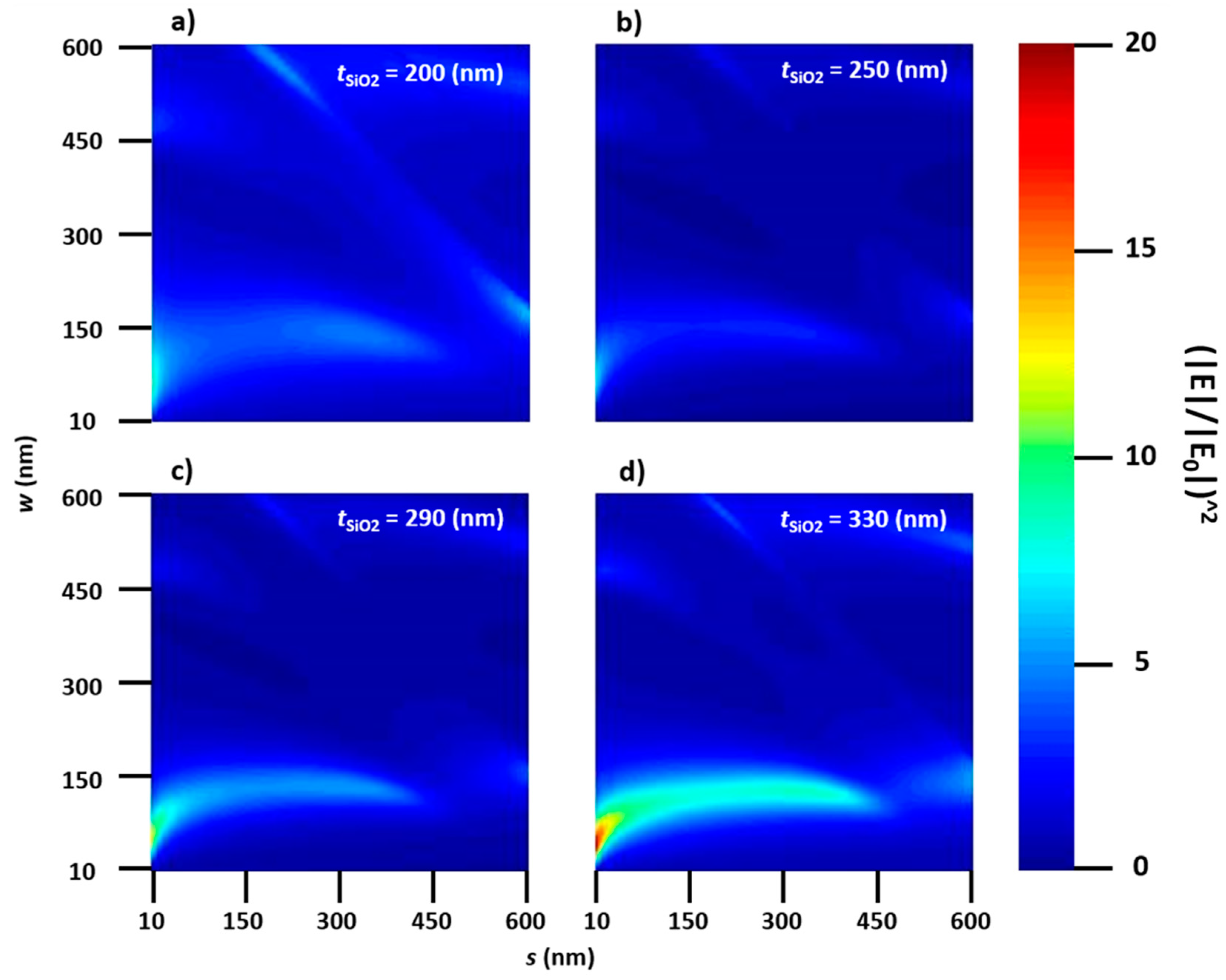
There are many potential benefits to SERS in plasmonics; however, most studies have been concerned with distances between plasmonic structures below 100 nm. In [19], we see that there are modes of plasmonic interference at some widths and spacings significantly greater than 100 nm that also induce strong electric fields. While not as strong as optimal widths and spacings, they can provide optical enhancement up to 11 times that of a similar surface with no plasmonic enhancement [19]. Due to the difficult nature of fabricating structures on the nanometer scale, these findings could be valuable to fabrication techniques in which it is easier to make larger structures.
The intent of this paper is to increase the reproducibility of the work achieved in [19]. We hope to elucidate our methods and computational models to create a framework which other computational plasmonics researchers can follow to build on or validate our work. The data is published in a text file format to make it accessible to researchers who may not have access to or experience with the COMSOL Multiphysics software package. The base COMSOL model is also made available for other work that may want to use and modify them for new geometries and studies. We hope that other computational methods, such as FDTD, can produce similar results and thus encourage more research in the field of plasmonic SERS substrates.
Supplementary Materials
The following are available online at: https://osf.io/6vb2w/?view_only=7629f06f081541968dbe986951167c4e (the dataset accompanying this paper will be available on the website).
Author Contributions
J.B.H. and C.M.K. decided to share data via open access, C.M.K. exported and organized data from model simulations, Z.T.B., J.B.H., S.J.B., and A.A.D. created the models, Z.T.B., S.J.B., and A.A.D. completed the experiments, C.M.K., Z.T.B., and D.T.D., analyzed the data, J.B.H. performed supervision, C.M.K. created original manuscript, J.B.K., Z.T.B., and S.J.B. provided revisions for manuscript.
Funding
This research was funded by NSF/EEC grant number 1757979, as well as partly by the Arkansas Biosciences Institute. S.J. Bauman received funding from the Doctoral Academy Fellowship via the University of Arkansas Graduate School in addition to the SPIE Optics and Photonics Education Scholarship. A. Darweesh had funding due to the Iraqi Ministry of Higher Education and Scientific Research (MoHESR). The University of Arkansas through the Department of Physics, the Fulbright College of Arts and Sciences, and the Office of Research & Innovation also provided funding and general research assets.
Acknowledgments
The Micro Electronics and Photonics Research Experience for Undergraduates, as well as the NSF, deserve acknowledgment for the support and opportunity that made this possible.
Conflicts of Interest
The authors declare no conflict of interest.
References
- Wang, A.X.; Kong, X. Review of recent progress of plasmonic materials and nano-structures for surface-enhanced Raman scattering. Materials 2015, 8, 3024–3052. [Google Scholar] [CrossRef] [PubMed]
- Kneipp, J.; Kneipp, H.; Kneipp, K. SERS—A single-molecule and nanoscale tool for bioanalytics. Chem. Soc. Rev. 2008, 37, 1052–1060. [Google Scholar] [CrossRef] [PubMed]
- Long, J.; Yang, T. Observation of single molecule dynamic behaviors with SERS: Desorption and conformation switching. In Proceedings of the Conference on Lasers and Electro-Optics (CLEO), San Jose, CA, USA, 5–10 June 2016; pp. 1–2. [Google Scholar]
- Sharma, B.; Frontiera, R.R.; Henry, A.-I.; Ringe, E.; van Duyne, R.P. SERS: Materials, applications, and the future. Mater. Today 2012, 15, 16–25. [Google Scholar] [CrossRef]
- Vo-Dinh, T. SERS chemical sensors and biosensors: New tools for environmental and biological analysis. Sens. Actuators B Chem. 1995, 29, 183–189. [Google Scholar] [CrossRef]
- Motz, J.T.; Hunter, M.; Galindo, L.H.; Gardecki, J.A.; Kramer, J.R.; Dasari, R.R.; Feld, M.S. Optical fiber probe for biomedical Raman spectroscopy. Appl. Opt. 2004, 43, 542–554. [Google Scholar] [CrossRef] [PubMed]
- Faulds, K.; Smith, W.E.; Graham, D.; Lacey, R.J. Assessment of silver and gold substrates for the detection of amphetamine sulfate by surface enhanced Raman scattering (SERS). Analyst 2002, 127, 282–286. [Google Scholar] [CrossRef] [PubMed]
- Barbillon, G.; Sandana, V.E.; Humbert, C.; Bélier, B.; Rogers, D.J.; Teherani, F.H.; Bove, P.; McClintock, R.; Razeghi, M. Study of Au coated ZnO nanoarrays for surface enhanced Raman scattering chemical sensing. J. Mater. Chem. C 2017, 5, 3528–3535. [Google Scholar] [CrossRef]
- Gramotnev, D.K.; Bozhevolnyi, S.I. Plasmonics beyond the diffraction limit. Nat. Photonics 2010, 4, 83–91. [Google Scholar] [CrossRef]
- Schuller, J.A.; Barnard, E.S.; Cai, W.; Jun, Y.C.; White, J.S.; Brongersma, M.L. Plasmonics for extreme light concentration and manipulation. Nat. Mater. 2010, 9, 193–204. [Google Scholar] [CrossRef] [PubMed]
- Dai, D.; He, S. A silicon-based hybrid plasmonic waveguide with a metal cap for a nano-scale light confinement. Opt. Express 2009, 17, 16646–16653. [Google Scholar] [CrossRef] [PubMed]
- Lin, Q.-Y.; Li, Z.; Brown, K.A.; O’Brien, M.N.; Ross, M.B.; Zhou, Y.; Butun, S.; Chen, P.-C.; Schatz, G.C.; Dravid, V.P.; et al. Strong coupling between plasmonic gap modes and photonic lattice modes in DNA-assembled gold nanocube arrays. Nano Lett. 2015, 15, 4699–4703. [Google Scholar] [CrossRef] [PubMed]
- Kalachyova, Y.; Mares, D.; Lyutakov, O.; Kostejn, M.; Lapcak, L.; Švorčík, V. Surface Plasmon Polaritons on Silver Gratings for Optimal SERS Response. J. Phys. Chem. C 2015, 119, 9506–9512. [Google Scholar] [CrossRef]
- Ding, S.; You, E.-M.; Moskovits, M. Electromagnetic theories of surface-enhanced Raman spectroscopy. Chem. Soc. Rev. 2017, 46, 4042–4076. [Google Scholar] [CrossRef] [PubMed]
- Zhao, D.; Pinchuk, A.O.; McMahon, J.; Li, S.; Ausman, L.; Atkinson, A.; Schatz, G. Methods for Describing the Electromagnetic Properties of Silver and Gold Nanoparticles. Acc. Chem. Res. 2008, 41, 1710–1720. [Google Scholar] [CrossRef] [PubMed]
- Bohren, C.F.; Huffman, D.R. Absorption and Scattering of Light by Small Particles; Wiley: Hoboken, NJ, USA, 1983. [Google Scholar]
- Bauman, S.J.; Brawley, Z.T.; Darweesh, A.A.; Herzog, J.B. Substrate oxide layer thickness optimization for a dual-width plasmonic grating for surface-enhanced Raman spectroscopy (SERS) biosensor applications. Sensors 2017, 17, 1530. [Google Scholar] [CrossRef] [PubMed]
- Lyvers, D.P.; Moon, J.-M.; Kildishev, A.V.; Shalaev, V.M.; Wei, A. Gold nanorod arrays as plasmonic cavity resonators. ACS Nano 2008, 2, 2569–2576. [Google Scholar] [CrossRef] [PubMed]
- Brawley, Z.T.; Bauman, S.J.; Darweesh, A.A.; Debu, D.T.; Tork Ladani, F.; Herzog, J.B. Plasmonic Au Array SERS Substrate with Optimized Thin Film Oxide Substrate Layer. Materials 2018, 11, 942. [Google Scholar] [CrossRef] [PubMed]
- COMSOL, Inc. COMSOL Multiphysics Version 5.3a: RF Module. Available online: https://www.comsol.com/ (accessed on 25 July 2018).
- Brawley, Z.T.; Bauman, S.J.; Abbey, G.P.; Darweesh, A.A.; Nusir, A.I.; Manasreh, O.; Herzog, J.B. Modeling and optimization of Au-GaAs plasmonic nanoslit array structures for enhanced near-infrared photodetector applications. J. Nanophotonics 2017, 11, 016017. [Google Scholar] [CrossRef] [Green Version]
- Hatab, N.A.; Hsueh, C.-H.; Gaddis, A.L.; Retterer, S.T.; Li, J.-H.; Eres, G.; Zhang, Z.; Gu, B. Free-standing optical gold bowtie nanoantenna with variable gap size for enhanced Raman spectroscopy. Nano Lett. 2010, 10, 4952–4955. [Google Scholar] [CrossRef] [PubMed]
- Johnson, P.B.; Christy, R.W. Optical constants of the noble metals. Phys. Rev. B 1972, 6, 4370–4379. [Google Scholar] [CrossRef]
- Green, M.A.; Keevers, M.J. Optical properties of intrinsic silicon at 300 K. Prog. Photovolt. Res. Appl. 2007, 3, 189–192. [Google Scholar] [CrossRef]
- Gao, L.; Lemarchand, F.; Lequime, M. Refractive index determination of SiO2 layer in the UV/Vis/NIR range: Spectrophotometric reverse engineering on single and bi-layer designs. J. Eur. Opt. Soc. Rapid Publ. 2013, 8, 13010. [Google Scholar] [CrossRef]
Figure 1.
Schematics of the FEM model. (a) 3D schematic of the SERS substrate structure which is modeled using a (b) 2D cross-section simulation. Structure consisting of a Si substrate with a SiO2 thin film on top and Au nanowires bonded with a Ti adhesion to layer the SiO2 thin film layer. Variables swept include the gold nanowire width (w), the spacing between electrodes (s), and the thickness of the SiO2 thin film (tSiO2). The incident light direction and polarization is shown. Note: Ti adhesion layer is not visible in (a).

Figure 2.
Graphical output of FEM plotting the electric field distribution of the optical enhancement of the simulation space of a periodic SERS substrate with the following variables: w = 10 nm, s = 70 nm, and tSiO2 = 200 nm. Please note that this plot shows the full width of the model, but it does not show the full height.

Figure 3.
Graphical renderings of average optical surface enhancement of s against w for varying tSiO2 values: (a) tSiO2 = 200 nm; (b) tSiO2 = 250 nm; (c) tSiO2 =290 nm; and (d) tSiO2 = 330 nm.
Figure 3.
Graphical renderings of average optical surface enhancement of s against w for varying tSiO2 values: (a) tSiO2 = 200 nm; (b) tSiO2 = 250 nm; (c) tSiO2 =290 nm; and (d) tSiO2 = 330 nm.


Table 1.
Data for the file fig_1b_w50 as it appears in the rows beginning on line 10. Please note that values in the figure are restricted to first four decimals for brevity.
Table 1.
Data for the file fig_1b_w50 as it appears in the rows beginning on line 10. Please note that values in the figure are restricted to first four decimals for brevity.
| x | y | Real (Ex) | Imag (Ex) | Real (Ey) | Imag (Ey) | Real (Ez) | Imag (Ez) |
|---|---|---|---|---|---|---|---|
| −30 | −530 | −0.0799 | 0.3404 | −6.6255 × 10⁻⁴ | 0.0017 | 0 | 0 |
| −30 | −511.8181 | −0.2425 | 0.2516 | −2.5247 × 10⁻⁴ | 1.9505 × 10⁻⁴ | −1.9377 × 10⁻¹⁸ | −2.4711 × 10⁻¹⁷ |
| −30 | −494.4976 | −0.3350 | 0.1007 | 1.9317 × 10⁻⁵ | −7.0334 × 10⁻⁵ | −3.2628 × 10⁻¹⁸ | −4.1869 × 10⁻¹⁷ |
© 2018 by the authors. Licensee MDPI, Basel, Switzerland. This article is an open access article distributed under the terms and conditions of the Creative Commons Attribution (CC BY) license (http://creativecommons.org/licenses/by/4.0/).
Share and Cite
MDPI and ACS Style
Klenke, C.M.; Brawley, Z.T.; Bauman, S.J.; Darweesh, A.A.; Debu, D.T.; Herzog, J.B. Dataset for SERS Plasmonic Array: Width, Spacing, and Thin Film Oxide Thickness Optimization. Data 2018, 3, 37. https://doi.org/10.3390/data3030037
AMA Style
Klenke CM, Brawley ZT, Bauman SJ, Darweesh AA, Debu DT, Herzog JB. Dataset for SERS Plasmonic Array: Width, Spacing, and Thin Film Oxide Thickness Optimization. Data. 2018; 3(3):37. https://doi.org/10.3390/data3030037
Chicago/Turabian StyleKlenke, Christopher M., Zachary T. Brawley, Stephen J. Bauman, Ahmad A. Darweesh, Desalegn T. Debu, and Joseph B. Herzog. 2018. "Dataset for SERS Plasmonic Array: Width, Spacing, and Thin Film Oxide Thickness Optimization" Data 3, no. 3: 37. https://doi.org/10.3390/data3030037