
Annealing Effects of ZnO Thin Film on Photocatalytic Performances of Graphene Composites


Department of Physical Science and Engineering, Nagoya Institute of Technology, Nagoya 466-8555, Japan
*
Author to whom correspondence should be addressed.
C 2024, 10(1), 4; https://doi.org/10.3390/c10010004
Submission received: 17 November 2023
/
Revised: 23 December 2023
/
Accepted: 27 December 2023
/
Published: 29 December 2023
Abstract
:The hybrid structure of Graphene and ZnO (Graphene/ZnO) is emerging as a novel material used to achieve the high performance of photocatalysis. In this study, we examined the ZnO characteristics that affect the photocatalytic activity of graphene/ZnO using a lamellar structure of graphene and ZnO thin films. Graphene samples were synthesized via chemical vapor deposition, and a typical wet process was applied to transfer them on sputter-deposited ZnO thin films with and without annealing. We confirmed that graphene-deposited ZnO demonstrated more efficient photocatalytic behavior toward the decomposition of methylene blue (as a model organic compound) with ordinary sputtered ZnO thin films. Again, ZnO thin films annealed at 1000 °C in an N2 gas atmosphere with graphene performed better than unannealed films. XRD analysis confirmed that pre-thermal treatment of a ZnO thin film promoted re-crystallization, which had less impact on the photocatalytic improvement. The attachment of graphene to the film is considered to contribute to the enhancement. Raman analysis revealed that the graphene coverage areas on the post-annealed ZnO increased by two times compared to that of an unannealed film where the unannealed film had a higher graphene layer. The results presented in this study demonstrate that an annealed ZnO thin film forms a better attachment with graphene, resulting in a larger graphene coverage area with fewer multilayers, which effectively improves the photocatalytic activity in composite structures.
1. Introduction
Recently, there has been significant interest in the exploration of cutting-edge nanocomposite materials and the advancement of their associated technologies [1]. Energy, hydrogen production, environmental issues, disinfection, and purification are just a few of the many domains in which a wide range of nanocomposites with various properties have been developed. These include metal-semiconductor nanocomposites [1], a range of metal oxides [2], and a combination of inorganic and organic materials [3]. Graphene, a two-dimensional material consisting of a honeycomb arrangement of carbon atoms, holds significant potential in various sectors of the medicinal and energy industries, such as photocatalysis, sensors, and membranes, due to its expansive surface area, higher conductivity, and chemical stability [4,5,6,7,8]. It is also possible to use efficient solar energy in nanotube formation [9,10]. In the context of photocatalysis applications, integrating monolayer graphene with semiconductors can enhance light absorption and expand charge-carrier lifetimes, thereby boosting photocatalytic performance [11]. Among the various methods for producing high-quality graphene on a large scale [11,12,13,14,15,16] and the production of a thin layer of graphene, the chemical vapor deposition (CVD) technique is a widely used and well-accepted technique in technological fields of materials processing [17,18,19,20,21,22,23], allowing to produce high-quality graphene with large-sized, well-crystallized structures at low cost [24,25,26,27,28,29].
Due to the exceptional surface reactivity, increased efficiency, and potent oxidation capabilities for decomposing organic molecules, zinc oxide (ZnO) has drawn interest as a potential metal semiconductor in the field of photocatalysis [30]. It possesses unique physical and chemical characteristics, such as diverse structures, simplified manufacturing methods, eco-friendliness, and excellent electron mobility [31]. For the effective elimination of Bisphenol A (BPA), Yujie Wang et al. have effectively created a porous ZnO photocatalyst with a core-shell structure and a wide surface area [32]. ZnO is also used in sensors, solar cells, optoelectronic devices, and photocatalytic processes due to its wide range of properties [33,34,35]. The amalgamation of graphene and ZnO has been shown to enhance photocatalytic efficacy. As of now, very few studies have demonstrated the impact of ZnO properties, such as crystal size, energy bandgap, film thickness, and so forth, in conjunction with graphene properties, such as surface area, crystallinity, grain boundaries, and layer count, on the photocatalytic efficiency of ZnO-graphene composites.
In this research study, we explored how the properties of ZnO influence the improvement in photocatalytic performance using a basic combination of a ZnO thin film and graphene. Monolayer graphene was deposited on a ZnO thin film, whose properties were changed through thermal annealing. The photocatalytic activity was tested via decomposing methylene blue dyes to discuss the photocatalytic performance of the ZnO-graphene composites. This article also illustrates the number of layers, grain boundaries, and graphene coverage areas throughout ZnO film surfaces. The outcome of this study demonstrates that annealed ZnO thin film forms a better attachment with graphene, resulting in a larger graphene coverage area with fewer multilayers, which leads to an effective improvement of the photocatalytic activity in composite structures.
2. Experimental
2.1. Materials
Copper foil, Acetone (C3H6O), Poly (methyl methacrylate) (PMMA), Iron nitrate enneahydtrate (Fe (NO3)3·9H2O), and C-plane sapphire substrate were purchased from “FUJIFILM Wako Pure Chemical Corporation”.
2.2. ZnO Thin Film Preparation
A ZnO target with an RF magnetron sputtering system and an experimental sapphire substrate—more precisely, a C-plane sapphire—was used within the chamber. The chamber was evacuated to 5.0 × 10⁻⁴ Pa of pressure using a diffusion pump while keeping the substrate and target 50 mm apart. During a 10-min sputtering procedure at a working power of 100 W, sputtering gases comprising 4.3 sccm of argon and oxygen of 1.1 sccm were used, which were controlled by a gas flow meter. The resultant substrate was utilized to cause morphological changes in seed layers after being used as a sample for an experiment. This sample was annealed in an N2 gas environment at 1000 °C. After that, the annealed substrate was utilized as a different trial for building composite structures and transporting them out for more photocatalytic research. The atomic force microscope (AFM) photographs of seed layers without heat treatment revealed granular surfaces; the size and roughness of these granules depended on the film thickness. Seed layers treated at 200–600 °C showed somewhat better crystallinity, according to Qiyan Zhang et al.’s findings [36]. We used comparable procedures, tools, and conditions to retain the same thickness of the ZnO thin film for our work. But at temperatures between 800 and 1000 °C, the seed layer surfaces became smooth and had crystals orientated along the C-axis; this led to better FWHM (full-width half maximum) values and smoother surfaces overall. Different material qualities and surface integrity features are characterized by the FWHM (Full Width at Half Maximum) of XRD profiles [37]. The relationship between crystalline size and FWHM is inversely proportional, as stated in Scherrer’s equation. It means the physical crystalline structures of nanoparticles from XRD peaks will be higher if the FWHM becomes lower. The same relationship has been shown by Mitsuhiro et al. [38]. To develop ZnO-Graphene composites independently and examine the influences of ZnO thin films on these composites, we had to decide between two preferences for ZnO thin films—untreated and treated—at 1000 °C in an N2 gas atmosphere.
2.3. Selection of Annealing Temperatures
For the feasibility of understanding, a ZnO thin film has been annealed at 1000 °C as it is the optimum annealing temperature compared with non-annealed. The reason for selecting 1000 °C is because Qiyan Zhang et al. had stated in [36] and Mitsuhiro et al. stated in [38] that the RF magnetron sputtered ZnO thin film annealed at 1000 °C exposes the highest crystalline size against the minimum of FWHM values in XRD. Those experiments were carried out at different annealing temperature ranges, i.e., 400 °C, 600 °C, 800 °C, and 1000 °C. The target of their experiments was to make the c-axis orientation of the ZnO seed layer. When a temperature higher than 600 °C was applied, the ZnO crystals were completely c-axis oriented. The structure of ZnO nanorods that were further grown on such annealed films was 800–1000 °C. Therefore, the temperature stopped increasing by more than 1000 °C. The lowest values of grain size and agglomeration of the film exhibited at 1000 °C annealed ZnO, including the surface roughness, are the fewest in Atomic Force Microscope (AFM) images. From [36], it has been found that for the 50 nm and 150 nm thick ZnO thin film, with optimum conditions for diameter and densities, the nanorod has been synthesized from the 1000 °C annealed ZnO thin film. So, the application of films is also found at their peak conditions at 1000 °C. Due to these behaviors of the ZnO thin film annealed at 1000 °C, we also chose the same values in this experiment.
The annealing effects of ZnO thin film were irreversible. Hypothetically, if any film meets the environment (air, water, etc.) after synthesis, then it gets contaminated and degrades its quality in the case of annealed or unannealed. The ZnO thin film sample we used for our experiments was always kept inside the vacuum chamber. After the sample, which was collected from the RF magnetron, was sputtered and after annealing the sample, we immediately kept it inside the vacuum chamber. The preserved samples inside the vacuum chamber were used for different experiments at different times. For example, when synthesized at the same time, some samples were used for some experiments immediately, and some samples were used for the same or different experiments after a few days. However, the performance and results of the samples were the same. It means the performance of the sample was not degraded, and the annealing effects were not reversible. So, we can say that the annealing effects were irreversible in our experiments.
2.4. Graphene Synthesis via CVD Method
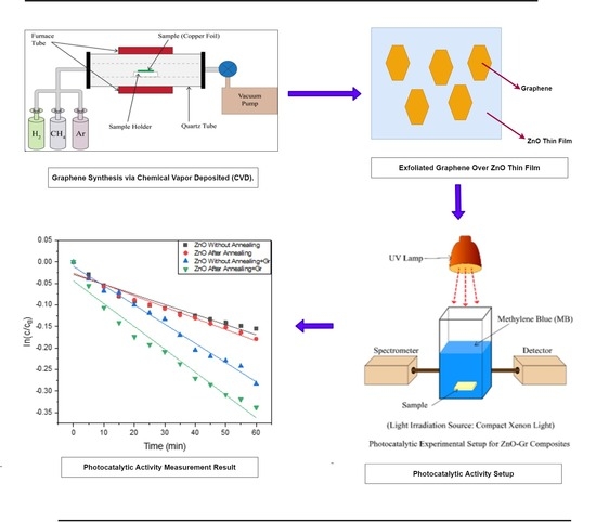
Figure 1 shows a diagram illustrating the CVD configuration used to produce graphene on Copper (Cu) foil. A copper foil with a surface area of (1 × 1) cm2 and a thickness of about 10μm was used as the substrate to develop graphene on its surface. The temperature at which the chemical vapor deposition (CVD) technique was carried out was 950 °C. Specific gas parameters were used in the CVD process: 100, 80, and 20 standard cubic centimeters per minute (sccm) of H2, Ar, and CH4 were supplied, respectively. The pressure inside the CVD chamber was kept at 77 Pa for 15 min when the CVD process was conducted.
2.5. Exfoliation of Graphene Layer from Copper Foil
Graphene must be separated from copper foil after it has been synthesized and placed onto a ZnO thin film in order to evaluate the composite structure’s photocatalytic capabilities. Poly (methyl methacrylate) (PMMA) was used as a support in a copper etching procedure that we used to exfoliate the graphene from the copper foil. The etchant used in this method was iron nitrate enneahydrate Fe (NO3)3·9H2O. The procedure is depicted in Figure 2. First, the graphene-covered copper foil’s upper surface was treated with a small amount of liquid PMMA (5 μL). The structure was heated on a hot plate for 2 h at 120 °C to guarantee good adhesion between PMMA and graphene. After that, the (PMMA + Graphene + Copper) structures were kept undisturbed for 15 h in a row with a solution of 0.1M Fe (NO3)3·9H2O added. The structure is normally rather buoyant and can float in the solutions; therefore, it is imperative to take care at this point to prevent the solution from coming in touch with the upper surfaces. After this stage, the Fe (NO3)3·9H2O solution completely dissolved the copper foil, leaving just the (PMMA + Graphene) floating in the solution because of its lightweight. The lower part of the graphene, known as PMMA + Graphene, was thoroughly cleaned by repeatedly washing it in distilled water and nitric acid (HNO3). For the following experimental procedures, (PMMA + Graphene) was deposited onto the ZnO thin film and heated on a hot plate at 120 °C for 60 min to ensure a secure attachment to the substrate and prevent it from dissolving in the photocatalytic reagent during measurements of photocatalytic activity. Acetone was used to wash graphene to remove any remaining PMMA and provide a clean top surface. PMMA is successfully dissolved using acetone without interacting with graphene. After this procedure, the ZnO thin-film graphene is prepared for characterization and more research.
2.6. ZnO-Graphene Composite Preparations
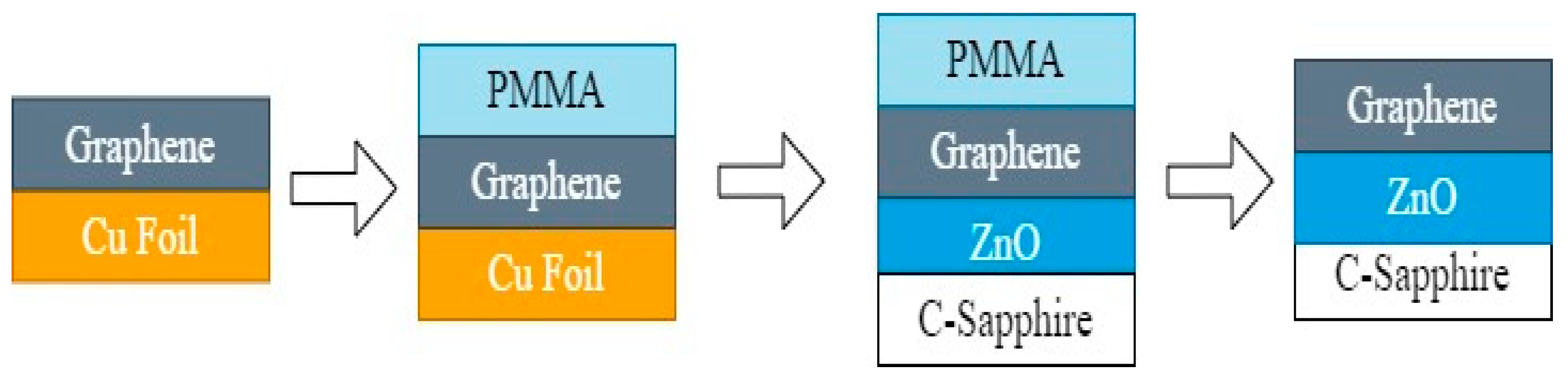
The synthesized graphene sheets were placed on both annealed and unannealed ZnO thin films. The ZnO thin film was the substrate in this instance, but the PMMA-assisted copper etching technique that was utilized to transfer the graphene has been described in Section 2.5. The process for making ZnO-Graphene composites after graphene exfoliations is shown in Figure 3. ZnO-Graphene composites were formed by applying two different conditions to the ZnO thin film to receive the exfoliated graphene. These included the use of two ZnO thin films: one that had not been annealed at all and one that had been annealed for 1.30 h at 1000 °C while N2 gas was present.
2.7. Experimental Setup for Photocatalytic Activity Measurement
The photocatalysis experimental arrangement is shown in Figure 4. It uses a 10-ppm methylene blue solution as the material for photocatalyst degradation and a small xenon lamp as the light source. The sample is submerged in the methylene blue solution under the UV lamp, and light is then detected using halogen and deuterium lamps, respectively, after passing through a spectrometer. Testing samples for the study come from four distinct periods: ZnO thin film without post-magnetron sputtering annealing (also called ZnO); ZnO thin film annealed at 1000 °C while N2 gas is present (also called ZnO-AA); ZnO thin film without annealing with graphene; and ZnO thin film following graphene annealing.
2.8. Material Characterization Apparatus
X-ray diffraction (XRD) analysis was performed on the acquired products using a Rigaku Smart Lab X-ray diffractometer fitted with a Cu target (λ = 1.5408 Å). Using a JEOL-6700F instrument, manufactured by JEOL, Tokyo, Japan. Scanning electron microscopy (SEM) (JSM-7800F, manufactured by JEOL, Tokyo, Japan) was used to analyze the sample’s physical structure. Optical measurements were made using a spectrophotometer at incidence over 200–800 nm a wavelength range, specifically measuring transmittance T (λ) and absorbance A (λ). A Shimadzu UV mini-1240 spectrophotometer was used to measure the absorbance of the methylene blue solution via UV-Vis absorption to quantify its concentration and evaluate the outcomes of photocatalyst degradation.
3. Results
Optical images and the Raman Spectrum of graphene at three different places are shown in Figure 5a,b. For clarity, three independent points of various peaks are provided in the inset of Figure 5b (top to down for points 1, 2 and 3). A minor D peak can be seen at 1345 cm−1, which is in line with the optimal placements for graphene and 2D Raman peaks located at 1580 cm−1 and 2685 cm−1, respectively. The strength of the 2D peak is notably equivalent to or higher than that of the G peak, suggesting that the generated graphene is not always purely monolayer after the Chemical Vapor Deposition (CVD) procedure. Graphene can be monolayer or bilayer across the surfaces, or it can show several layers in some cases, as demonstrated by the Ig/I2d ratio being below 2. For instance, bilayer or multilayer graphene is indicated at specific locations where the 2D peak is smaller than or equal to the G peak. The different ratios of bilayer and multilayer graphene can be explained by the existence of graphene grain boundaries, which can act as growth sites for multilayer graphene. On a single-crystalline copper foil, however, a bigger sheet of monolayer or bilayer graphene was seen. The 2D peak is substantially higher than the G peak only in a few selected spots, indicating the presence of monolayer graphene.
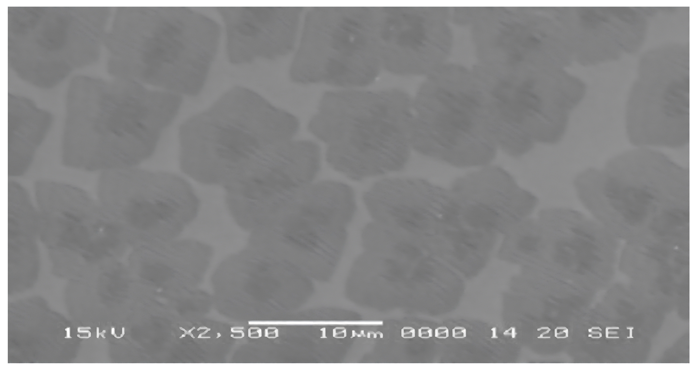
At higher magnification levels, Figure 6 shows the intricate morphological structures of the graphene on copper foil. The graphene has been manufactured and maintained with a high degree of success over the surface of the copper substrate. The graphene produced by CVD has a diameter of around 10 μm and is composed of multilayer structures in the center and monolayer edges. The existence of graphene grain boundaries at the core nucleation sites is responsible for this variation.
The XRD data for the ZnO thin film produced by RF magnetron sputtering are shown in Figure 7a, and b for unannealed and annealed, respectively. The ZnO thin film’s crystalline sizes were calculated using Scherrer’s equations. Scherrer’s equation can be used to determine a crystalline material’s average crystallite size, sometimes referred to as the crystallite diameter or crystallite domain size. Examining the spreading peaks in its X-ray diffraction patterns allows for investigation. Scherrer’s equation is given by,
where K = Scherrer’s constant, usually the value of this constant is 0.94 [39]. λ is the wavelength of the X-ray radiation used for diffraction. Here, for copper K-alpha, the wavelength of the X-ray will be 1.5406 Å, the default value of the wavelength of LASER, which is mostly used in the instrument. β is the Bragg angle, full width at half maximum (FWHM) of the diffraction peak (in radians). θ have been considered from the 2θ values of the XRD graph. The curve fitting was performed first, and then the exact values were confirmed using Equation (1) to find out the crystalline sizes. Findings show that the ZnO thin film that was first made, as shown in Figure 7a, has a polycrystalline structure with a hexagonal (wurtzite) crystal orientation, especially in the (002) direction. The ZnO thin film’s shape is changed by annealing it again at 1000 °C in an N2 gas environment, and the ZnO-Graphene composites changes are monitored. The ZnO peaks can be seen in both images at angles of 31.2°, 34.52°, and 72.78°, respectively, at locations like 100, 002, 004, and a few more. With the JCPDS card No. 05-0664, a comparison of the measured and standard ‘d’ values was carried out. Based on the observation of a strong ZnO peak in both figures at the 002 position (34.52°), we may deduce that the films have desirable properties, indicating that they should be investigated further. Moreover, annealing improves the crystalline sizes and full width at half maximum (FWHM), according to the rise in ZnO intensity peaks at the same locations following the annealing procedure. Table 1 shows the FWHM and crystalline sizes of the ZnO thin film for both conditions after performing the curve fittings. We can observe from Table 1 that when the ZnO thin film is annealed, it increases in crystalline size from 27.62 nm to 39.27 nm, but its full width at half maximum (FWHM) value drops. This behavior is probably caused by the heat treatment procedure, which thickens the flow in the vicinity of the substrate contact, causing the grain size to reorganize and the crystalline size to rise [40].
Graphene was removed from the copper substrate using the PMMA-supported copper etching approach and then applied to the ZnO surface to form composite structures of ZnO-Graphene. Figure 8 shows the Raman spectra of the graphene transferred in (a) non-annealed and (b) post-annealed situations to evaluate the success of the graphene transfer. From Raman spectra, graphene and 2D peaks are located at different locations, which are in line with their positions before the exfoliation process. At the same time, the ZnO thin-film Raman peaks are unaltered, suggesting that the substrate is not harmed. The pre-exfoliation locations of both peaks on the ZnO thin film are aligned with their placements; nevertheless, the intensity of the 2D peak is lower than that of the graphene peak. This observation suggests that graphene was successfully transferred onto the ZnO thin film, although some wrinkling is still noticeable. There is a little peak that appears to represent PMMA residues following exfoliation, although it is barely noticeable in comparison to the G and 2D peaks. Compared to the unannealed ZnO thin film, G and 2D peaks for the ZnO annealed sample contain graphene, which is more prominent. This property implies that, in comparison to its unannealed counterpart, annealed ZnO develops better bonding with graphene.
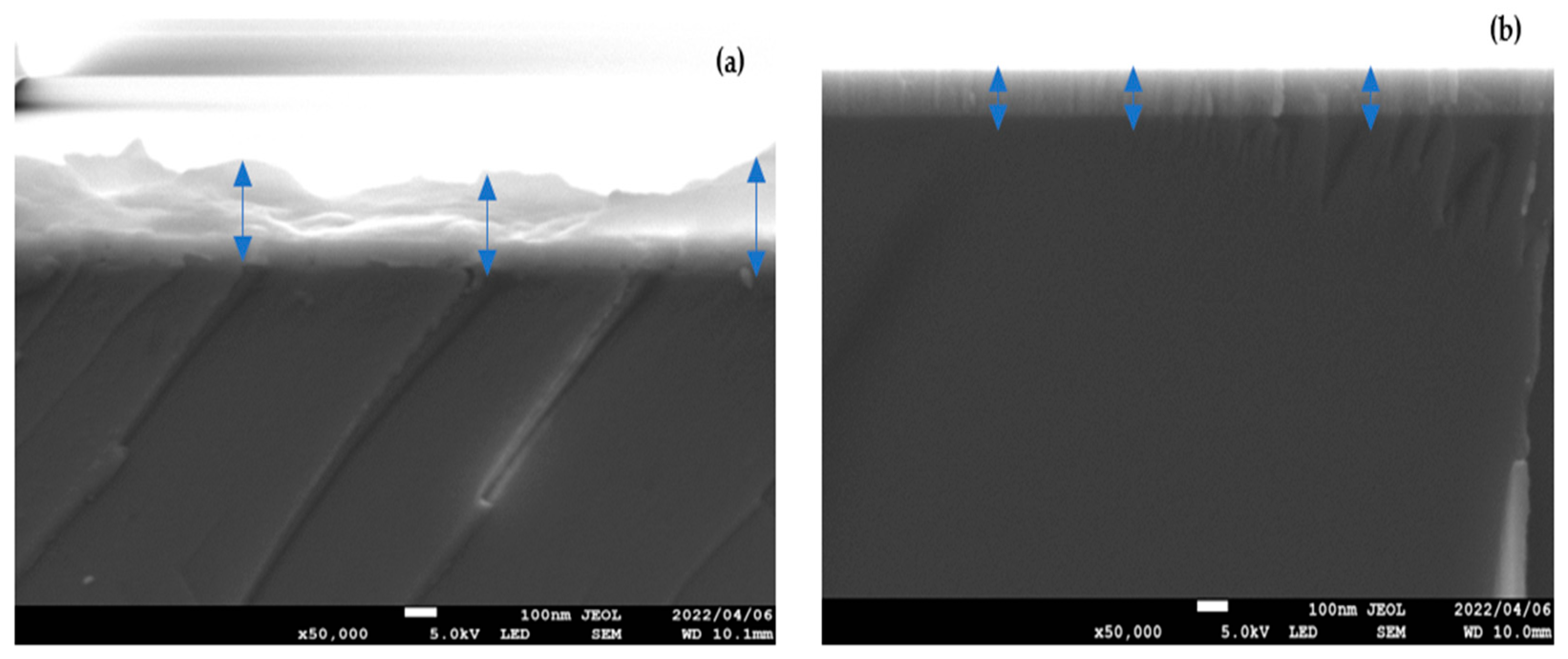
The photocatalytic experiment investigated four different samples. An annealed ZnO thin film at 1000 °C (ZnO-AA), a sputtered ZnO thin film with graphene (ZnO-WA + Gr), and graphene with the ZnO thin film after annealing at 1000 °C (ZnO-AA + Gr) are among them. The photocatalytic performance curves with error bars using normalized data are shown in Figure 9. The rate constants and photodegradation rates were computed using the data taken from Figure 9 to create Table 2. Compared to its non-annealed counterpart, the annealed ZnO thin film demonstrates improved photocatalytic activity, improving the concentration ratio by over 1.12 times, according to an assessment of Figure 9 and Table 2. However, significant improvements in photocatalytic activities are seen when graphene is added to ZnO thin films of comparable diameters. Meanwhile, a ZnO thin film with graphene (ZnO-WA + Graphene) shows 1.91 times higher activity than a bare ZnO thin film. Again, ZnO annealed at 1000 °C with graphene (ZnO-AA + Graphene) reveals more than 2.25 times more photocatalytic activity than the ZnO thin film. This implies that enhanced photocatalytic performance is mostly attributed to the addition of graphene to the ZnO thin film. We will discuss more about the underlying causes of this improvement in later sections, along with how annealing affects the ZnO thin film when combined with graphene. Figure 10a,b show the cross-sectional images from SEM to show the thickness of the ZnO thin film without annealing or after annealing indicated by blue arrows. The uneven edges and surfaces of the thin film are visible in Figure 10a, giving the impression that it is not smooth. Additionally, the film’s thickness varies from 150 to 200 nm, showing non-uniformity in areas less than 150 nm and others around 150 nm. The film is seen to be almost flat in Figure 10b, with noticeably smoother surfaces and edges because of the annealing process. Annealing the film at 1000 °C in an N2 gas environment results in a homogenous, high-quality, flat film, even though its thickness reduces. According to this, annealing helps create a thin, uniform, and flat film surface, which improves adhesion with graphene and, as a result, improves photocatalytic activity.
The decrease in the ZnO thin film’s bandgap from 3.28 eV to 3.12 eV upon annealing is depicted in Figure 11a,b. The absorbance measurements were used to create the bandgap curve. The arrows have been used to determine the values of bandgap from x-axis. The reduction of the energy band gap is a significant factor in increasing photocatalytic activity. The ZnO thin film annealed with high temperature is probably the cause of the energy band gap fall, as shown in Figure 11. This suggests that greater light absorption capacity and, thus, higher photocatalytic activity are caused by a lower bandgap between the valence and conduction bands. The crystal lattice’s expansion and the interatomic bonds’ weakening with rising temperatures may be the causes of this behavior. As a result, less energy is required to break a bond and elevate an electron into the conduction band. To fully analyze the factors influencing the enhanced photocatalytic activity, the structural properties of graphene were thoroughly investigated in conjunction with the ZnO thin film. The impact of annealing of the film on several factors was examined, including the graphene coverage area, graphene layers, graphene attachment to the ZnO thin film, the presence of grain boundaries of graphene, etc.
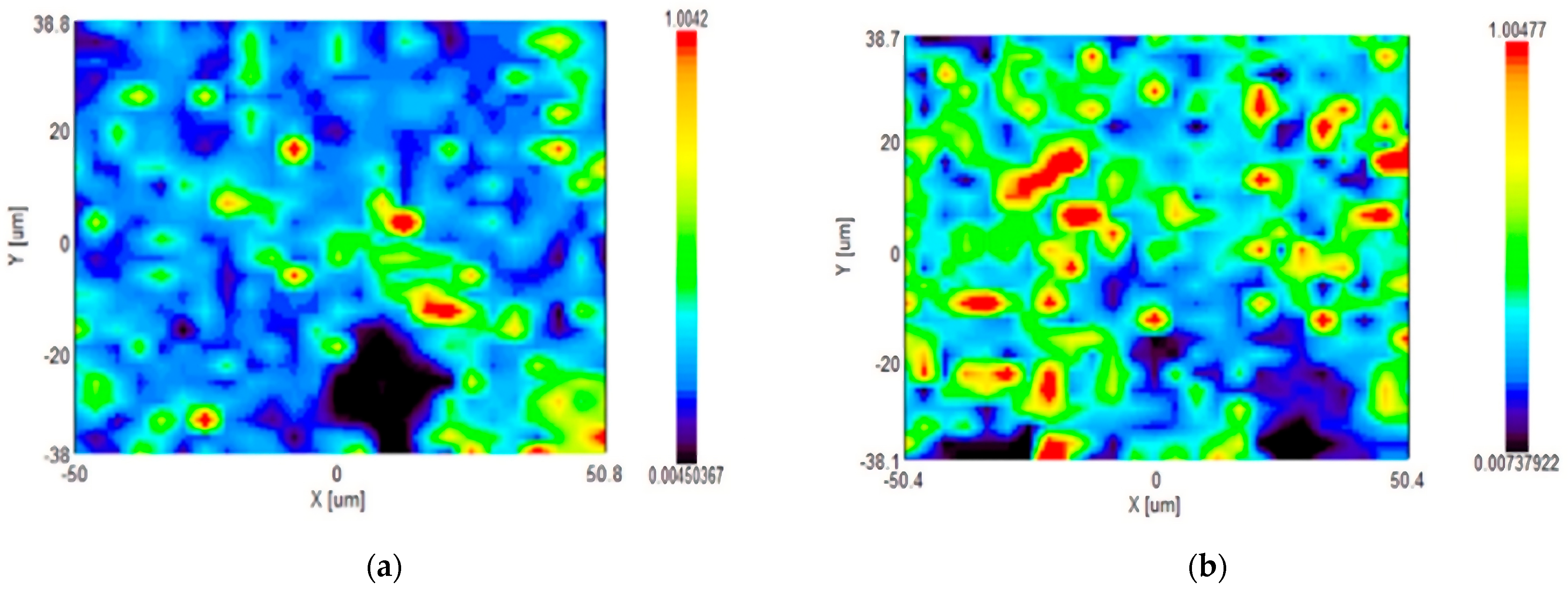
The distribution of graphene in the ZnO-Graphene composites, both for the as-prepared thin film and after annealing, is depicted in Figure 12a,b using Raman mapping pictures. This information sheds light on the coverage areas of graphene and layer number over ZnO. Notably, as shown in Figure 12, the post-annealed ZnO thin film shows more extensive graphene covering, perhaps because of the smoother surface attained during annealing. For both cases, the number of graphene layers and the existence of grain boundaries of graphene over ZnO are given in Table 3 and Table 4. The graphene attachment to the unannealed ZnO thin film is comparatively modest, Table 3 shows, occupying only 23% of the film’s surface area.
Most regions of the ZnO thin film do not have graphene superimposed on them. Moreover, just 11% of the surface has a single layer of graphene, and 28% has two layers, accounting for about 61% of the surface’s multiple layers. On the other hand, the graphene coverage area of the annealed ZnO thin film is much larger, covering almost 63% of the surface. The monolayer percentages of graphene in post-annealed ZnO thin films rise to roughly 26%, whereas double and multilayers are 42% and 32%, respectively. Table 4 shows that annealing of the film improves graphene adherence to the film surface, which reduces graphene wrinkling over the entire film. In addition, post-annealed ZnO thin films have more pronounced graphene grain boundaries around their periphery than unannealed films. Here, In Table 4, the reaction rate has been calculated from the photodegradation of the sample using first-order kinetics. The equation for 1st order kinetic rate is given below:
Using this equation and then considering the slope values of the logarithm of output values, the reaction rate has been found. We considered two different samples, (i) Unannealed ZnO-Graphene and (ii) Annealed ZnO-Graphene, for the comparison to understand the differences in reaction rate. The absorbance data was taken for 1 h at a stretch by keeping the initial values as 1 (reference value), at which every 5 min data of the sample was considered. Again, the annealed film exhibits graphene grain boundaries of around 45.24 μm in length, whereas the ZnO thin film achieves grain boundaries of about 29.59 μm. The annealed ZnO thin film surface could be the cause of the decreased presence of multilayer graphene in the film. Graphene sticks more firmly and does not wrinkle or form several layers because of its smoother surface and lower, consistent thickness. On the other hand, wrinkling and the development of multilayer graphene are caused by the unannealed ZnO thin film’s uneven thickness and rougher surface, which make it difficult to achieve a strong graphene attachment. For 1 h of UV radiation, graphene containing the ZnO thin film (both unannealed and annealed) showed better photocatalytic activity than the as-prepared film. This is because graphene has higher quantities of light absorption, greater charge carrier separation, and larger amounts of charge transportation, etc. These characteristics of graphene over the film surfaces increased the light absorptions and reduced recombination of the photo-generated electrons and holes in ZnO; hence, the decomposition of photodegradation material, i.e., methylene blue has increased, and the photocatalytic performance also enhanced. Again, the better performance of graphene-containing the annealed ZnO thin film than the unannealed is because of the better adhesions of graphene over the annealed ZnO thin film. This results in better attachments and higher coverage areas of graphene over the film surfaces. Again, poor adhesion for the unannealed film results in higher wrinkles, which results in a higher number of graphene layers with less coverage area and, ultimately, poor photocatalytic performances.
From Figure 12, we can see that the larger graphene coverage area and higher number of monolayer graphene result in higher photocatalytic activity. In this experiment, the graphene over copper foil after chemical vapor deposition (CVD) synthesis for both cases was the same before the exfoliations, as in both cases, the same graphene was used. However, the graphene coverage areas and number of layers over the film after the exfoliations were different due to the differences in the attachment of graphene over the film. The annealed film exposes higher coverage areas of graphene than the unannealed film, indicating that better attachment has been achieved due to the annealing of the sample. The layer numbers, i.e., bilayer or multilayer of graphene, were higher in the unannealed sample. This has happened due to the poor attachment of graphene with the film surfaces. Because the unattached graphene was wrinkled and formed layers within the film surfaces, this also led to the increment of graphene grain boundaries over the film. So, it can easily be said that the poor attachment of the exfoliated graphene with the film substrates is mostly responsible for decreasing the graphene coverage area, increasing layer numbers and grain boundaries; hence, decreasing photocatalytic performances.
4. Conclusions
In conclusion, we have successfully demonstrated the formation of lamellar structures of ZnO thin films and graphene via a typical wet transfer process. The chemical vapor depositions (CVD) graphene was successfully synthesized over the copper foil method and effectively exfoliated from the copper using the supported cu etching method. Annealing was performed on prepared ZnO thin films to investigate its impact on the photocatalytic properties of ZnO-graphene composite materials. Annealing the ZnO thin film induced alterations in its crystalline structure, thickness, and energy bandgap. These modifications facilitated the formation of a strong interface with graphene sheets, along with achieving a larger coverage area, an increased number of monolayers, and higher graphene grain boundaries. The deposition of graphene on a ZnO thin film was observed to provide a higher photocatalytic activity through decomposing MB dye. Consequently, the enhancement of photocatalysis is expected to contribute to the overall improvement of photocatalytic performance.
Author Contributions
Conceptualization, J.A.R., M.H. and Y.I.; methodology, J.A.R., M.H. and Y.I.; validation, J.A.R., M.H. and Y.I.; formal analysis, J.A.R., Y.K., M.H. and Y.I.; investigation, J.A.R., Y.K., M.H. and Y.I.; resources, J.A.R., Y.K., M.H. and Y.I.; data curation, J.A.R., M.H. and Y.I.; writing—original draft preparation, J.A.R. and M.H.; writing—review and editing, J.A.R., M.H. and Y.I.; visualization, J.A.R., Y.K., M.H. and Y.I.; supervision, M.H. and Y.I. All authors have read and agreed to the published version of the manuscript.
Funding
This research received no external funding.
Data Availability Statement
Data are contained within the article.
Acknowledgments
The characterization equipment (Raman Spectrum and XRD Analysis) was supported by the Equipment Sharing Division, Organization for Co-Creation Research and Social Contributions, Nagoya Institute of Technology. Special thanks to “Masaki Tanemura” for the “SEM measurement” and his tremendous support and guidance throughout this work.
Conflicts of Interest
The authors declare no conflict of interest.
References
- Lee, J.M.; Pyun, Y.B.; Yi, J.; Choung, J.W.; Park, W., II. ZnO Nanorod−Graphene Hybrid Architectures for Multifunctional Conductors. J. Phys. Chem. 2009, 113, 19134–19138. [Google Scholar] [CrossRef]
- Lin, J.; Penchev, M.; Wang, G.; Paul, R.K.; Zhong, J.; Jing, X.; Ozkan, M. Heterogeneous Graphene Nanostructures: ZnO Nanostructures Grown on Large-Area Graphene Layers. J. Nano Micro Small 2010, 6, 2448–2452. [Google Scholar] [CrossRef]
- Kim, Y.-J.; Hadiyawarmam; Yoon, A.; Kim, M.; Yi, G.-C.; Liu, C. Hydrothermally grown ZnO nanostructures on few-layer graphene sheets. J. Nanotechnol. 2011, 22, 245603. [Google Scholar] [CrossRef]
- Chandandraiahgari, C.R.; De Bellis, G.; Balijepalli, S.K.; Kaciulis, S.; Ballirano, P.; Migliori, A.; Morandi, V.; Caneve, L.; Sarto, F.; Sarto, M.S. Control of the size and density of ZnO-nanorods grown onto graphene nanoplatelets in aqueous suspensions. J. RSC Adv. 2016, 6, 83217–83225. [Google Scholar] [CrossRef]
- Gon, K.J.; Byungrak, S.; Santanu, M.; Nicholas, S.; Alex, B.; Osung, K.; Jong, C.M.; Yeol, C.H.; Sam, P. A review of lithium and non-lithium based solid state batteries. J. Power Sources 2015, 282, 299–322. [Google Scholar]
- Scrosati, B.; Garche, J. Lithium Batteries: Status, Prospects and Future. J. Power Sources 2010, 195, 2419–2430. [Google Scholar] [CrossRef]
- Raub, A.A.M.; Yunas, J.; Mohamed, M.A.; Kazmi, J.; Ridwan, J. Structural and Optical Properties Investigation of Graphene Oxide coated ZnO nanorods for Enhanced Photocatalytic Effect. In Proceedings of the 2021 IEEE Regional Symposium on Micro and Nanoelectronics (RSM), Kuala Lumpur, Malaysia, 2–4 August 2021; pp. 104–107. [Google Scholar]
- Machado, B.F.; Serp, P. Graphene-based mater ials for catalysis. J. Catal. Sci. Technol. 2012, 2, 54–75. [Google Scholar] [CrossRef]
- Islam, M.A.; Al Rafi, J.; Uddin, M.A. Modeling and formation of a single-walled carbon nanotube (SWCNT) based heterostructure for efficient solar energy: Performance and defect analysis by numerical simulation. AIP Adv. 2023, 13, 115201. [Google Scholar] [CrossRef]
- Uddin, M.A.; Rafi, J.A.; Islam, M.A.; Mominuzzaman, S.M.; Nath, I.D. Modeling and Numerical Analysis of Heterostructure Single-Walled Carbon Nanotube (SWCNT) Solar Cell. In Proceedings of the 2022 12th International Conference on Electrical and Computer Engineering (ICECE), Dhaka, Bangladesh, 21–23 December 2022; pp. 388–391. [Google Scholar]
- Xiang, Q.; Yu, J.; Jaroniec, M. Graphene-based semiconductor photocatalysts. Chem. Soc. Rev. 2012, 41, 782–796. [Google Scholar] [CrossRef]
- Wang, Z.G.; Chen, Y.F.; Li, P.J.; Hao, X.; Liu, J.B.; Huang, R.; Li, Y.R. Flexible graphene-based electroluminescent devices. ACS Nano 2011, 5, 7149–7154. [Google Scholar] [CrossRef]
- Eda, G.; Fanchini, G.; Chhowalla, M. Large-area ultrathin films of reduced graphene oxide as a transparent and flexible electronic material. Nat. Nanotechnol. 2008, 3, 270–274. [Google Scholar] [CrossRef] [PubMed]
- Yin, Z.; Sun, S.; Salim, T.; Wu, S.; Huan, X.; He, Q.; Lam, Y.M.; Zhang, H. Organic photovoltaic devices using highly flexible reduced graphene oxide films as transparent electrodes. ACS Nano 2010, 4, 5263–5268. [Google Scholar] [CrossRef]
- Wu, Y.; Lin, Y.M.; Bol, A.A.; Jenkins, K.A.; Xia, F.; Farmer, D.B.; Zhu, Y.; Avouris, P. High-frequency, scaled graphene transistors on diamond-like carbon. Nature 2011, 472, 74–78. [Google Scholar] [CrossRef] [PubMed]
- Neto, A.H.C.; Guinea, F.; Peres, N.M.; Novoselov, K.S.; Geim, A.K. The electronic properties of graphene. Rev. Mod. Phys. 2009, 81, 109–162. [Google Scholar] [CrossRef]
- Geim, A.K. Graphene: Status and Prospects. Science 2009, 324, 1530–1534. [Google Scholar] [CrossRef]
- Novoselov, K.S.; Geim, A.K.; Morozov, S.V.; Jiang, D.; Zhang, Y.; Dubonos, S.V.; Grigorieva, I.V.; Firsov, A.A. Electric field in atomically thin carbon films. Science 2014, 306, 666–669. [Google Scholar] [CrossRef]
- Reina, A.; Jia, X.; Ho, J.; Nezich, D.; Son, H.; Bulovic, V.; Dresselhaus, M.S.; Kong, J. Large area, few-layer graphene films on arbitrary substrates by chemical vapor deposition. Nano Lett. 2009, 9, 30–35. [Google Scholar] [CrossRef]
- Gao, L.; Guest, J.R.; Guisinger, N.P. Epitaxial graphene on Cu (111). Nano Lett. 2010, 10, 3512–3516. [Google Scholar] [CrossRef]
- Choucair, M.; Thordarson, P.; Stride, J.A. Gram-scale production of graphene based on solvothermal synthesis and sonication. Nat. Nanotechnol. 2009, 4, 30–33. [Google Scholar] [CrossRef]
- Wang, X.; You, H.; Liu, F.; Li, M.; Wan, L.; Li, S.; Li, Q.; Xu, Y.; Tian, R.; Yu, Z.; et al. Large-Scale Synthesis of Few-Layered Graphene using CVD. Chem. Vap. Depos. 2009, 15, 53–56. [Google Scholar] [CrossRef]
- Al Rafi, J.; Islam, A.; Nuzhat, T.; Honda, M.; Ichikawa, Y. Effects of Argon (Ar) on Synthesis and Photocatalytic Activities of Graphene. IEEE Trans. Nanotechnol. 2023, 22, 321–327. [Google Scholar] [CrossRef]
- Ismach, A.; Druzgalski, C.; Penwell, S.; Schwartzberg, A.; Zheng, M.; Javey, A.; Bokor, J.; Zhang, Y. Direct chemical vapor deposition of graphene on dielectric surfaces. Nano Lett. 2010, 10, 1542–1548. [Google Scholar] [CrossRef]
- Sattler, K.D. Carbon Nanomaterials. In Sourcebook: Graphene, Fullerenes, Nanotubes, and Nanodiamonds, 1st ed.; Taylor and Francis Group: Boca Raton, FL, USA, 2016; Volume I, p. 630. [Google Scholar]
- Hirata, M.; Gotou, T.; Horiuchi, S.; Fujiwara, M.; Ohba, M. Thin-film particles of graphite oxide. 1: Highyield synthesis and flexibility of the particles. Carbon 2014, 42, 2929–2937. [Google Scholar] [CrossRef]
- Ehrentraut, D.; Sato, H.; Kagamitani, Y.; Sato, H.; Yoshikawa, A.; Fukuda, T. Solvothermal growth of ZnO. Prog. Cryst. Growth Charact. Mater. 2006, 52, 280–335. [Google Scholar] [CrossRef]
- Wang, L.; Tang, K.; Zhang, M.; Xu, J. Facile synthesis of Mn-doped ZnO porous nanosheets as anode materials for lithium-ion batteries with a better cycle durability. Nanoscale Res. Lett. 2015, 3, 3–7. [Google Scholar] [CrossRef]
- Sagar, R.U.R.; Mahmood, N.; Stadler, F.J.; Anwar, T.; Navale, S.T.; Shehzad, K.; Du, B. High-capacity retention anode material for lithium-ion battery. Electrochim. Acta 2016, 21, 156–163. [Google Scholar] [CrossRef]
- Coleman, V.A.; Jagadish, C. Basic properties and applications of ZnO. In Zinc Oxide Bulk, Thin Films and Nanostructures: Processing, Properties, and Applications; Jagadish, S.P.E.C., Ed.; Elsevier Science Ltd.: Amsterdam, The Netherlands, 2006; Chapter 1; pp. 1–20. [Google Scholar]
- Oprea, O.; Andronescu, E.; Ficai, D.; Ficai, A.; Oktar, F.N.; Yetmez, M. ZnO applications and challenges. Curr. Org. Chem. 2014, 18, 192–203. [Google Scholar] [CrossRef]
- Wang, Y.; Hu, K.; Yang, Z.; Ye, C.; Li, X.; Yan, K. Facile Synthesis of Porous ZnO Nanoparticles Efficient for Photocatalytic Degradation of Biomass-Derived Bisphenol A Under Simulated Sunlight Irradiation. Front. Bioeng. Biotechnol. 2021, 8, 616780. [Google Scholar] [CrossRef]
- Janotti, A.; Van de Walle, C.G. Fundamentals of zinc oxide as a semiconductor. Rep. Prog. Phys. 2009, 72, 29. [Google Scholar] [CrossRef]
- Kołodziejczak-Radzimska, A.; Jesionowski, T. Zinc oxide—From synthesis to application: A review. Materials 2014, 7, 2833–2881. [Google Scholar] [CrossRef]
- Candal, R.; Martínez-de la Cruz, A. New Visible-Light Active Semiconductors. In Photocatalytic Semiconductors; Hernández-Ramírez, A., Medina-Ramírez, I., Eds.; Springer: Cham, Switzerland, 2015; pp. 41–67. [Google Scholar]
- Zhang, Q.; Honda, M.; Ichikawa, Y. Seed layer morphology influencing ZnO nanorod growth by hydrothermal synthesis. In Transactions of the Materials Research Society of Japan; The Materials Research Society of Japan: Yokohama, Japan, 2018; Volume 43, pp. 349–353. [Google Scholar]
- Vashista, M.; Paul, S. Correlation between full width at half maximum (FWHM) of XRD peak with residual stress on ground surfaces. Philos. Mag. 2012, 92, 4194–4204. [Google Scholar] [CrossRef]
- Honda, M.; Zhang, Q.; Tateyama, H.; Ichikawa, Y. Densely aligned ZnO nanoneedle arrays prepared via room temperature growth. J. Ceram. Soc. Jpn. 2018, 126, 367–371. [Google Scholar] [CrossRef]
- Thein, M.T.; Chim, J.E.; Pung, S.-Y.; Pung, Y.-F. Highly UV light driven WOx@ZnO nanocomposites synthesized by liquid impregnation method. J. Ind. Eng. Chem. 2017, 46, 119–129. [Google Scholar] [CrossRef]
- Lee, H.C.; Liu, W.-W.; Chai, S.-P.; Mohamed, A.R.; Lai, C.W.; Khee, C.-S.; Voona, C.H.; Hashim, U.; NHidayah, M.S. Synthesis of Single-layer Graphene: A Review of Recent Development. Procedia Chem. 2016, 19, 916–921. [Google Scholar] [CrossRef]
Figure 1.
Chemical Vapor Deposited (CVD) graphene synthesis on cu foil.
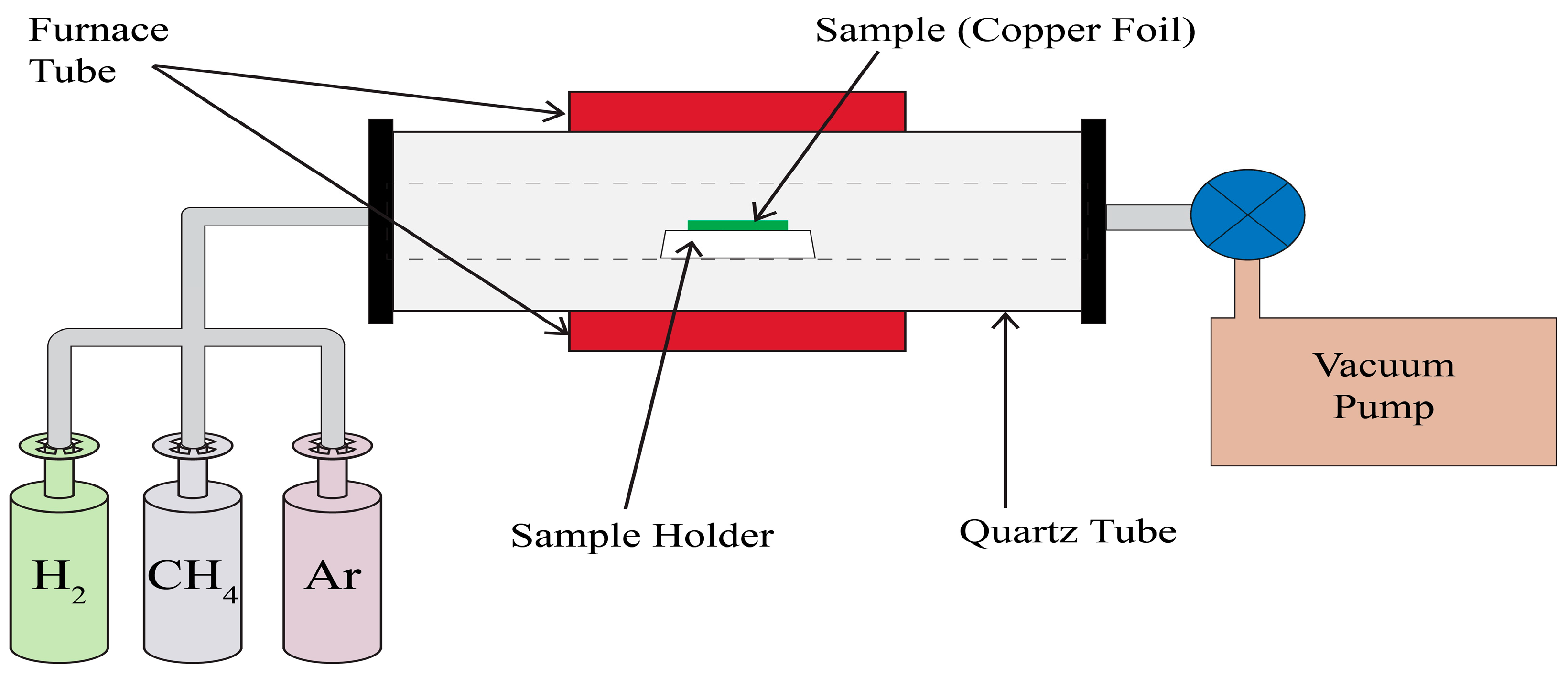
Figure 2.
Copper (cu) etching method to exfoliate graphene.
Figure 3.
Composite structures preparation processes.

Figure 4.
Experimental setup for Photocatalytic Activity Measurement.
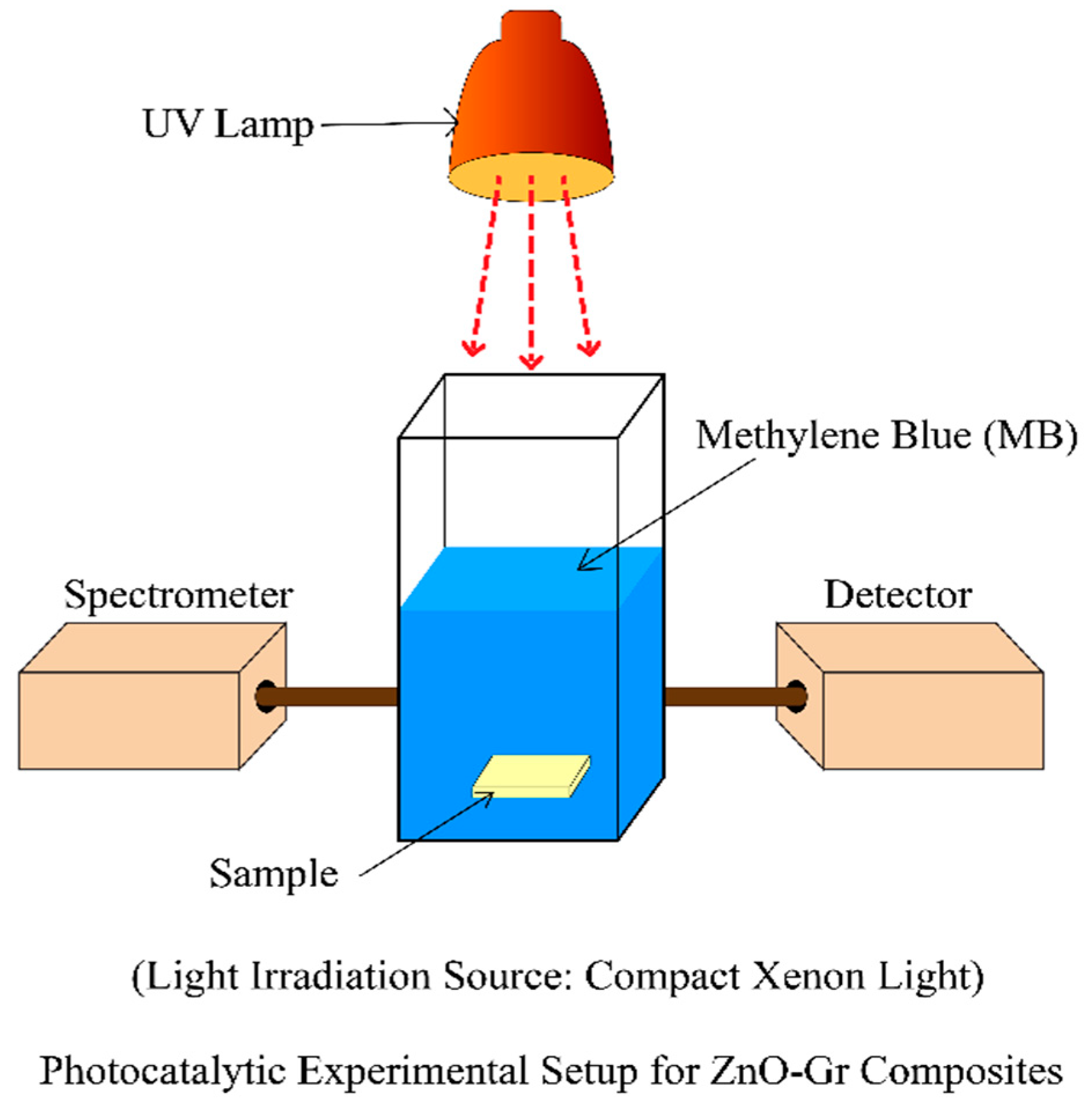
Figure 5.
(a) Raman optical images and (b) Spectrum of graphene.
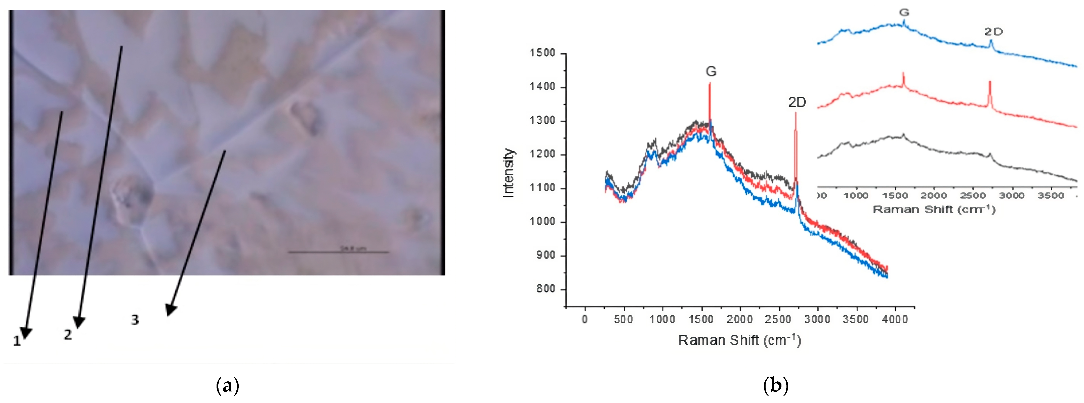
Figure 6.
CVD synthesized graphene SEM images.

Figure 7.
XRD pattern of ZnO thin film (a) without annealing, (b) annealed at 1000 °C.

Figure 8.
ZnO-Graphene Composite Raman Spectrum.
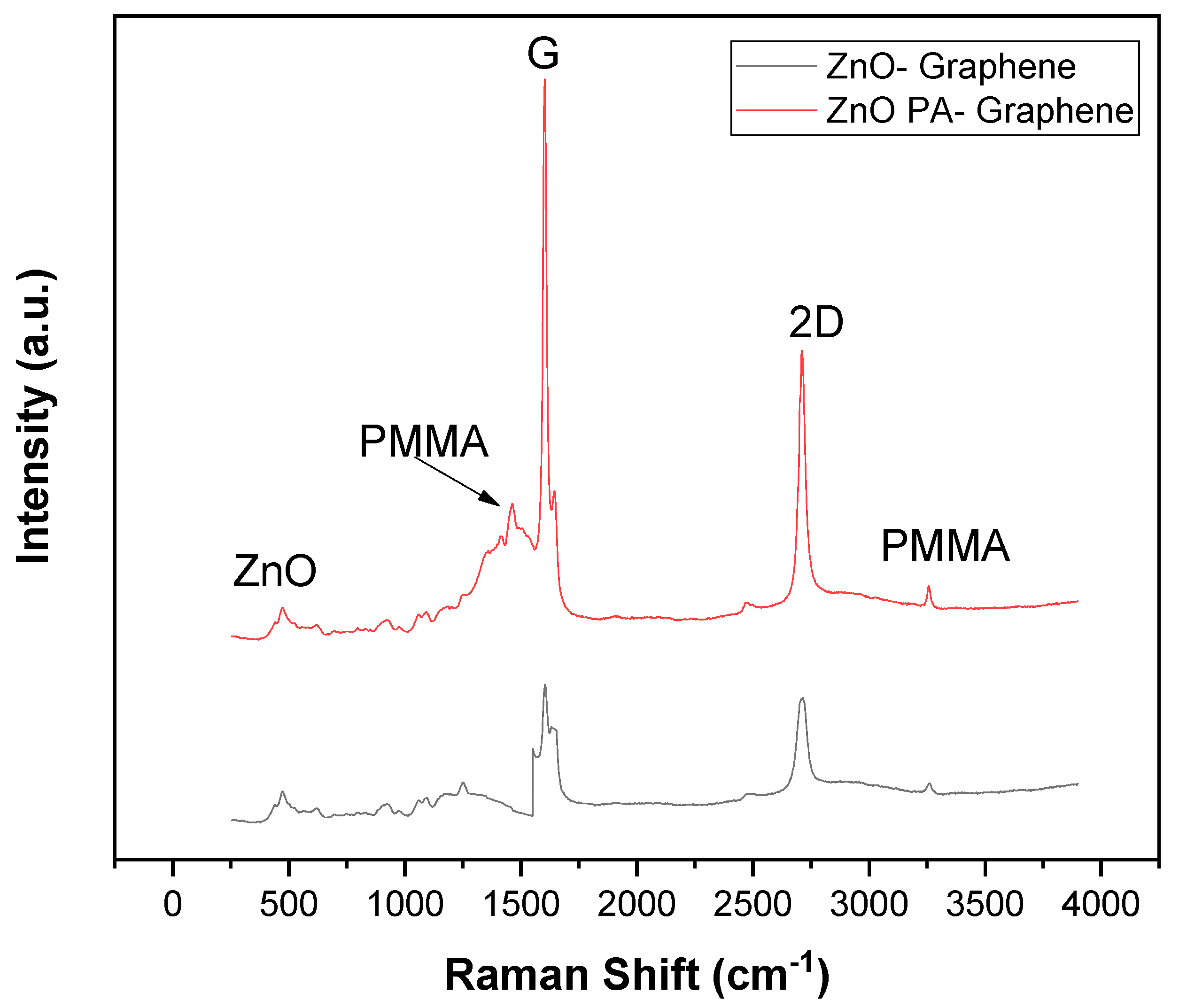
Figure 9.
ZnO-Gr composite photocatalytic activity results.
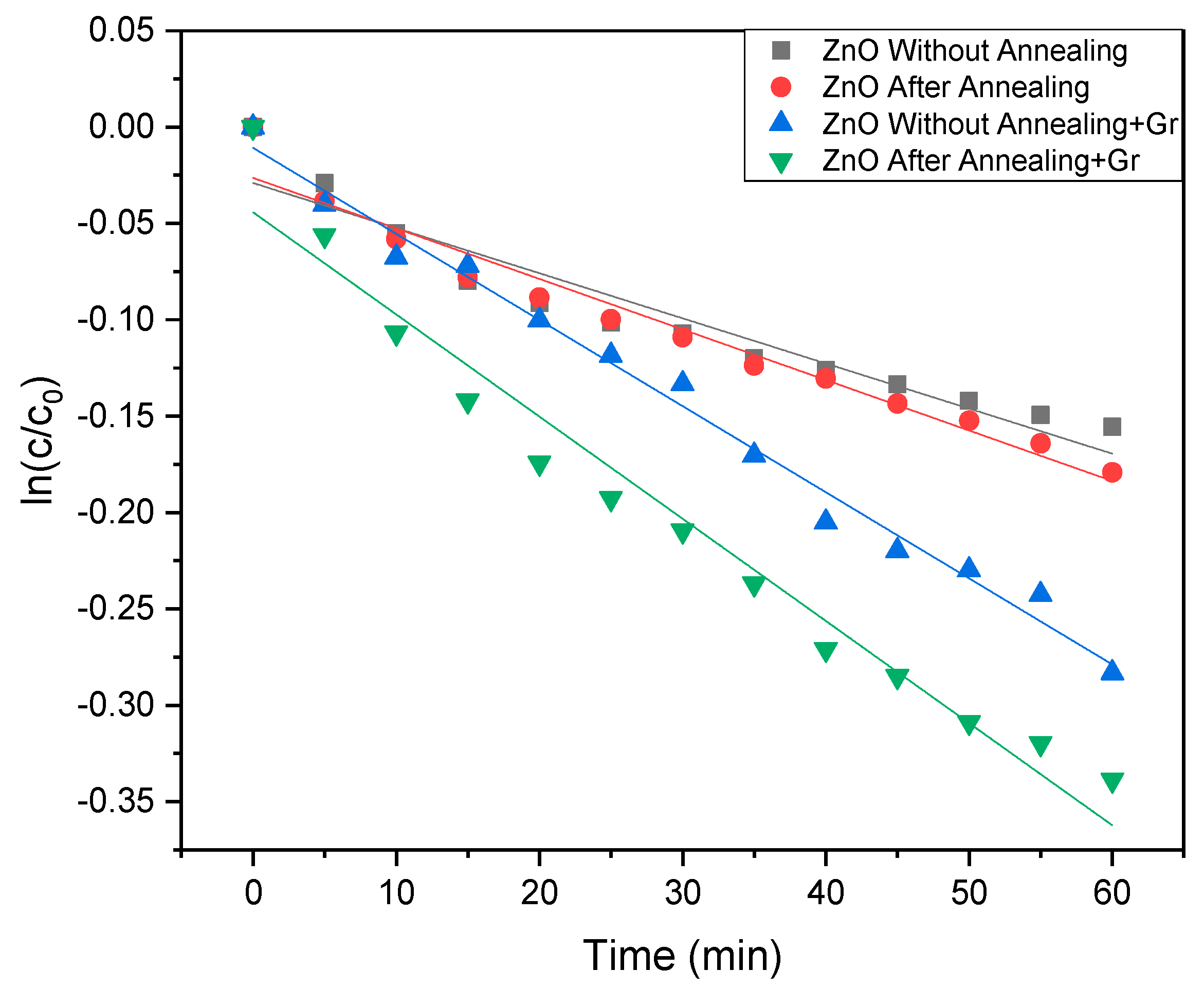
Figure 10.
ZnO Film thickness (a) without annealing (b) annealed at 1000 °C.

Figure 11.
Energy bandgap of ZnO thin film (a) without annealing, (b) annealed at 1000 °C.

Figure 12.
The coverage area of graphene over ZnO (a) without annealing (b) annealed at 1000 °C.


Table 1.
Crystalline sizes of ZnO thin film.
| Sample | FWHM | Crystalline Size (nm) |
|---|---|---|
| ZnO Thin Film | 0.31458 | 27.62 |
| Annealed ZnO Thin Film | 0.22133 | 39.27 |
Table 2.
ZnO-Gr composites concentration ratio.
| Sample | Constant Rate (C.R.) | C.R. Enhancement Compared to ZnO | %Photodegradation |
|---|---|---|---|
| ZnO Thin Film | 3.91 × 10⁻⁵/min | 1 | 14% |
| Annealed ZnO Thin Film | 4.36 × 10⁻⁵/min | 1.12 | 18% |
| ZnO Thin Film-Graphene | 7.45 × 10⁻⁵/min | 1.91 | 25% |
| Annealed ZnO Thin Film-Graphene | 8.83 × 10⁻⁵/min | 2.25 | 28% |
Table 3.
Graphene layer percentages over ZnO.
| Sample | Single Layer | Double Layer | Multilayer |
|---|---|---|---|
| ZnO Thin Film-Graphene | 11% | 28% | 61% |
| Annealed ZnO Thin Film-Graphene | 26% | 42% | 32% |
Table 4.
Graphene grain boundaries.
| Sample | Reaction Rate “k” (×10−5 min−1) | Perimeter (μm) |
|---|---|---|
| ZnO Thin Film-Graphene | 7.45 | 29.59 |
| Annealed ZnO Thin Film-Graphene | 8.83 | 45.24 |
Disclaimer/Publisher’s Note: The statements, opinions and data contained in all publications are solely those of the individual author(s) and contributor(s) and not of MDPI and/or the editor(s). MDPI and/or the editor(s) disclaim responsibility for any injury to people or property resulting from any ideas, methods, instructions or products referred to in the content. |
© 2023 by the authors. Licensee MDPI, Basel, Switzerland. This article is an open access article distributed under the terms and conditions of the Creative Commons Attribution (CC BY) license (https://creativecommons.org/licenses/by/4.0/).
Share and Cite
MDPI and ACS Style
Rafi, J.A.; Kanda, Y.; Honda, M.; Ichikawa, Y. Annealing Effects of ZnO Thin Film on Photocatalytic Performances of Graphene Composites. C 2024, 10, 4. https://doi.org/10.3390/c10010004
AMA Style
Rafi JA, Kanda Y, Honda M, Ichikawa Y. Annealing Effects of ZnO Thin Film on Photocatalytic Performances of Graphene Composites. C. 2024; 10(1):4. https://doi.org/10.3390/c10010004
Chicago/Turabian StyleRafi, Jobair Al, Yu Kanda, Mitsuhiro Honda, and Yo Ichikawa. 2024. "Annealing Effects of ZnO Thin Film on Photocatalytic Performances of Graphene Composites" C 10, no. 1: 4. https://doi.org/10.3390/c10010004
Note that from the first issue of 2016, this journal uses article numbers instead of page numbers. See further details here.