Imaging with a Commercial Electron Backscatter Diffraction (EBSD) Camera in a Scanning Electron Microscope: A Review


1
Department of Mining and Materials Engineering, McGill University, Montréal, QC H3A 0C5, Canada
2
Institut de Recherche d’Hydro-Québec, 1806 Boulevard Lionel-Boulet, Varennes, QC J3X 1S1, Canada
*
Author to whom correspondence should be addressed.
J. Imaging 2018, 4(7), 88; https://doi.org/10.3390/jimaging4070088
Submission received: 21 May 2018
/
Revised: 14 June 2018
/
Accepted: 20 June 2018
/
Published: 1 July 2018
(This article belongs to the Special Issue Phase-Contrast and Dark-Field Imaging)
Abstract
:Scanning electron microscopy is widespread in field of material science and research, especially because of its high surface sensitivity due to the increased interactions of electrons with the target material’s atoms compared to X-ray-oriented methods. Among the available techniques in scanning electron microscopy (SEM), electron backscatter diffraction (EBSD) is used to gather information regarding the crystallinity and the chemistry of crystalline and amorphous regions of a specimen. When post-processing the diffraction patterns or the image captured by the EBSD detector screen which was obtained in this manner, specific imaging contrasts are generated and can be used to understand some of the mechanisms involved in several imaging modes. In this manuscript, we reviewed the benefits of this procedure regarding topographic, compositional, diffraction, and magnetic domain contrasts. This work shows preliminary and encouraging results regarding the non-conventional use of the EBSD detector. The method is becoming viable with the advent of new EBSD camera technologies, allowing acquisition speed close to imaging rates. This method, named dark-field electron backscatter diffraction imaging, is described in detail, and several application examples are given in reflection as well as in transmission modes.
1. Introduction
Among the characterization tools available to the materials scientist, the scanning electron microscope (SEM) is probably the most used and versatile. It offers a spatial resolution in the sub-nanometer level when equipped with a cold-field emitter or a beam monochromator [1,2], and its design allows the analyst to observe the surface of a specimen from the nanometer to the centimeter range. Because the mean free path of low energy electrons is dramatically smaller than that of X-rays, the technique is the missing link between high penetration depth techniques like X-ray-based systems and atomic level surface techniques like atomic force microscopy or scanning tunneling microscopy. Thus, by varying the accelerating voltage (E0) applied to the electron beam and the type of signal collected, one can obtain “bulk” information; however, if lower voltages are used, the collected signals originate from the shallow surface layers [2]. For example, the range of electrons/material interactions at E0 = 20 kV in iron is roughly 1 µm, while it falls to 15 nm at E0 = 1 kV. Note that these numbers are maximum values and that the emission depth and lateral distribution may be further reduced depending on the type of signal that is collected to generate the image.
Technically speaking, in a SEM, a beam of focused electrons is scanned over a specimen surface in a raster fashion, and many different signals are collected to generate different images with various contrasts. These contrasts depend on the nature of the particle that is collected, as well as on the nature of the interaction that the particle has undergone during its path through the material. Secondary electrons are produced by the ejection of mostly valence electrons due to atomic ionization, and are characterized by their low energy and small inelastic mean free path, in addition to being highly absorbed before reaching the exit surface. Their emission depth is thus confined to surface layers—generally in the range of a few nanometers—depending on the atoms’ band structures and absorption, and they provide topographic contrast that allows us to observe the relief of the surface in a 3D-like fashion.
In contrast, the primary electrons that are backscattered towards the surface due to the atoms’ Coulomb attraction forces retain sufficient energy to reach the exit surface with limited absorption, and carry information about the composition of the volume of material “seen” by these electrons. These are called Backscattered Electrons (BSE), and are responsible for compositional contrast (also known as material or Z contrast), which is in fact related to the mean atomic number of the material interacting with them. Their emission depth and lateral distribution depend on the material characteristics and the primary beam accelerating voltage. The energy distribution of these BSEs being material and SEM parameters dependent, energy filtration allows us to collect only high energy BSEs, i.e., those with low-loss of energy, which are associated with high spatial resolution and reduced interaction volume. These low-loss electrons suffer a small number of interactions, and originate from the close surrounding of the beam impact point on the surface. The depth resolution is of the order of the mean free path, but depends mostly on the energy-loss considered.
Because they interact with the crystal lattice of the specimen through diffraction processes, the BSEs carry information about the crystallinity in their emission volume, but mostly from the exit surface. In the SEM, there are two ways of gathering the diffraction information carried by these electrons. In 1967, Coates evidenced the channeling of BSEs by imaging a Kikuchi-like patterns from Ge and GaAs crystals when the electron beam was scanned over the surface of the specimens at low magnification [3]. This type of pattern was later termed as an Electron Channeling Pattern (ECP); this led to the well-known electron channeling contrast imaging (ECCI). Later, in 1973, Venables and Hartland obtained similar patterns in spot mode when the specimen was highly tilted towards a phosphorescent screen, typically 60–70° [4]. At this time, the image was captured from a phosphorescent screen by means of an external camera. Currently, charge-coupled device (CCD) cameras are commonly used to capture these patterns with high speed rates [5]—up to 3000 patterns per second—to produce phase and orientation maps based on the crystallography and crystallographic orientation of the different phases present in the analyzed material.
This discovery resulted in one of the most important techniques in materials science, namely Electron Backscattered Diffraction (EBSD) [6], that is now widely used in the materials community to characterize microstructures at the sub-micron scale with spatial resolution roughly ranging from 20 to 150 nm, depending upon the material’s atomic number and density [7,8]. In this technique, the bands detected on the EBSD patterns (EBSP) are a projection of the crystal planes on the EBSD camera screen. They are processed and compared to a look-up table to match the most probable phase and orientation at each pixel. However, it took many years before the raw signal collected by the CCD cameras was used to generate images, the information gathered so far being mainly related to the bands detected on the EBSD pattern. In parallel, Prior and co-workers reported compositional and crystallographic orientation imaging when attaching solid state diodes just below and above the CCD screen [9]. They described a dramatic change in contrast when switching from the bottom to the top diodes to record the image. Top diodes provided compositional contrast, while those from the bottom resulted in orientation contrast. These findings were later confirmed and used by Payton et al. to help with phase identification when combined with EBSD indexing [10].
Recently, the use of the raw signal collected by the CCD camera was reported by several authors. In 2006, Wells and co-workers reported the first use of the EBSD camera as an imaging device, and more importantly, as a BSE angular distribution collector [11]. Following this route, Schwarzer and Sukkau demonstrated that imaging was possible by summing pixels from a specified region of the CCD camera and reconstructing the image based on the summed intensities [12,13], thus resulting in different contrasts depending on the pixels’ location, as later confirmed by Nowell and co-workers [14]. In 2015, Wright and co-workers reported the first commercial software proposing this facility in a live scanning mode or in post-processed mode [15]. However, the images thus obtained did not receive the attention required to properly understand the contrasts that were observed at that time. At the same time, Brodusch and co-workers reported a post-processed imaging technique based on EBSPs used to generate dark-field type images related to the specific diffraction conditions selected on the diffraction pattern [16,17]. They named this technique EBSD dark-field imaging mode (EBSD-DF). More recently, and following the work of Wells, De Graef and co-workers reported a method based on EBSPs to measure surface topography via the determination of surface normals [18], and reported nanometer scale spatial resolution comparable with atomic force microscopy on a Ni surface machined with a femtosecond laser [19].
In this contribution, we report on how to use the CCD camera of a commercial EBSD system as an imaging detector in various situations, and how relevant it is to understand and optimize the image contrasts. First, the method will be described in details and a program developed in Python language will be provided for the reprocessing of post-acquisition EBSD data. The usefulness of our approach will be demonstrated by applying this method to materials providing compositional, magnetic domain and diffraction/Z-contrasts.
2. Materials and Methods
2.1. Scanning Electron Microscopy
In this work, imaging and EBSD works were accomplished using a Hitachi SU8000 cold-field emission scanning electron microscope (Hitachi High-Tech, Tokyo, Japan) equipped with an Oxford Instruments EBSD system. The EBSD camera was a Nordlys II with dimensions of 28 × 38 mm² and was controlled by the Flamenco software, part of the HKL Channel 5 suite. The energy cut-off of the camera was estimated to be not higher than 1 keV from previous measurements [20]. The accelerating voltage was 30 kV, except when otherwise specified, and the specimens were tilted to 70° toward the EBSD camera, except for the transmission EBSD set-up where the tilt was −20°. Parameters for each EBSD scan are given in the result section when necessary. The acquisition of the ECP in was performed with a Hitachi SU3500 variable-pressure SEM using a solid-state BSE detector at E0 = 30 kV.
The X-ray images were obtained using a Bruker FlatQuad annular silicon drift detector (Bruker, Billerica, MA, USA) for energy dispersive spectrometer (EDS) attached to a Hitachi SU8230 cold-field emission scanning electron microscope. The accelerating voltage was 5 kV. Secondary electron (SE) images were acquired with an in-chamber Everhart-Thornley type detector providing BSE contrast due to the high number of SEs of type II and III (SEs generated by the BSEs inside and outside the specimen, respectively) collected by this detector.
For convention, the angle between the electron beam and the specimen surface normal directions is referred to θin while the angle made by the emitted BSEs with the specimen surface is referred to θout, as indicated in Figure 1a. In transmission mode, θout is referred to the angle between the transmitted electrons emission angle and the beam direction (Figure 1b). Hence, in this work, θin was 70° and −20° for conventional and transmission EBSD set-ups, respectively. θout may be calculated by simple geometric manipulations, and an example of a calibration curve relating the distance from the bottom of the EBSD camera screen with the corresponding θout is given in Figure 1c.
Bright-field (BF) images were recorded using the transmission mode of the SEM (STEM) with an yttrium aluminum garnet (YAG) scintillator detector located below the specimen around the optic axis of the microscope. An aperture was placed on top of the detector to select a BF collection angle of 10–20 mrad. The accelerating voltage was 30 kV. Note that the homemade sample holder used for this work allowed us to collect BF-STEM images and transmission EBSD (t-EBSD) data without any change of geometry or detector position, as described in a previous paper [21,22].
Monte Carlo simulations were conducted following the single scattering model as described by Gauvin and co-workers [23] using the screened Rutherford elastic cross-section expression and the Bethe continuous energy-loss equation, as modified by Joy and Luo [24]. The magnetic deflection was implemented following the procedure described by Newbury [25,26].
The image contrast C between regions A and B of an image was calculated using the following equation:
where IA and IB were the integrated intensities in area A and B, respectively.
In the case of magnetic domain contrast imaging (Section 3.3), a correction had to be applied to reduce the image tip noise generated by the cold-field emitter of the microscope [2]. This noise was observable because high gain needed to be applied to make the domain structure visible, as magnetic domain contrast with E0 = 30 kV and a tilt angle of 60° lies between 0.15% and 0.20%, as reported by Newbury [27]. This noise appears as intensity changes from line to line all along the captured image. The post-processing correction was accomplished with a simple procedure using a code written in Python language (www.python.org). For each line of the image, the mean intensity was calculated and compared to the previous line, the first line being the reference mean intensity. Note that any line could be selected as the reference if desired. Then, the brightness of the line was adjusted to fit its mean intensity to that of the previous line and the adjusted brightness factor was finally applied to each pixel of the line. This procedure allowed us to reduce greatly the tip noise observed although not completely.
2.2. Materials
The material used for the acquisition of the ECP and EBSP displayed in Figure 2 was a 1 × 1 cm² (001) oriented LaAlO3 single crystal provided by Alfa Aesar (Haverhill, MA, USA) (www.alfa.com). The application examples presented here were obtained on three different samples. The first was a piece of slag left over after melting lead-rich ores by early civilizations from Mexico. It was composed of mixed oxide and sulfide zinc/iron/lead-rich phases. The second sample was a non-oriented Fe-2.78%-Si electrical steel (NOES) on which magnetic domains were already observed and studied in a previous work [28]. These two samples were prepared by mechanical grinding and polishing down to 50 nm colloidal suspension, followed by ion milling with an accelerating voltage of 5 kV and an incident angle of 7° relative to the specimen surface. For this purpose, a Hitachi IM3000 (Hitachi High-Tech, Tokyo, Japan) flat milling system was used. The last sample was an AA2099 Al-Li-Cu alloy thinned to electron transparency by means of twin-jet electropolishing followed by ion milling at 2 kV accelerating voltage and 7° incidence angle on both sides of the foil.
2.3. Description of the Method
A full description of the method is available elsewhere [17], and only a short description is given here. The original method was based on the relation between the ECP and the EBSP, which are related by the accepted reciprocity theorem [29,30]. This relation explains that the two techniques should give identical patterns if the sources and detectors are switched when passing from one technique to the other. For sake of comparison, an EBSP and an ECP obtained from a (001) oriented LaAlO3 single crystal are shown in Figure 2a,b, respectively. Note the higher magnification of the ECP (Figure 2b), which is due to the limited SEM scanning angle available to generate the pattern. The angular resolution of the two recorded patterns, defined as the acquisition angular step, can be estimated by dividing the total collection angle by the number of pixels of the image x-axis. For this reason, the ECP exhibits an improved angular resolution compared to the EBSP, as recently demonstrated by Brodusch and co-workers in their Figure 2 [17]. However, if the EBSD detector distance is increased, the angular resolution becomes comparable, and the main features of the ECP are well reproduced in the EBSP. A comparison of orientation images obtained from ECCI and the corresponding image using the reconstruction method based on EBSP was reported by Kaboli and co-workers [31]. They demonstrated matching contrasts between the two images, confirming the equivalent information contained in the two types of patterns.
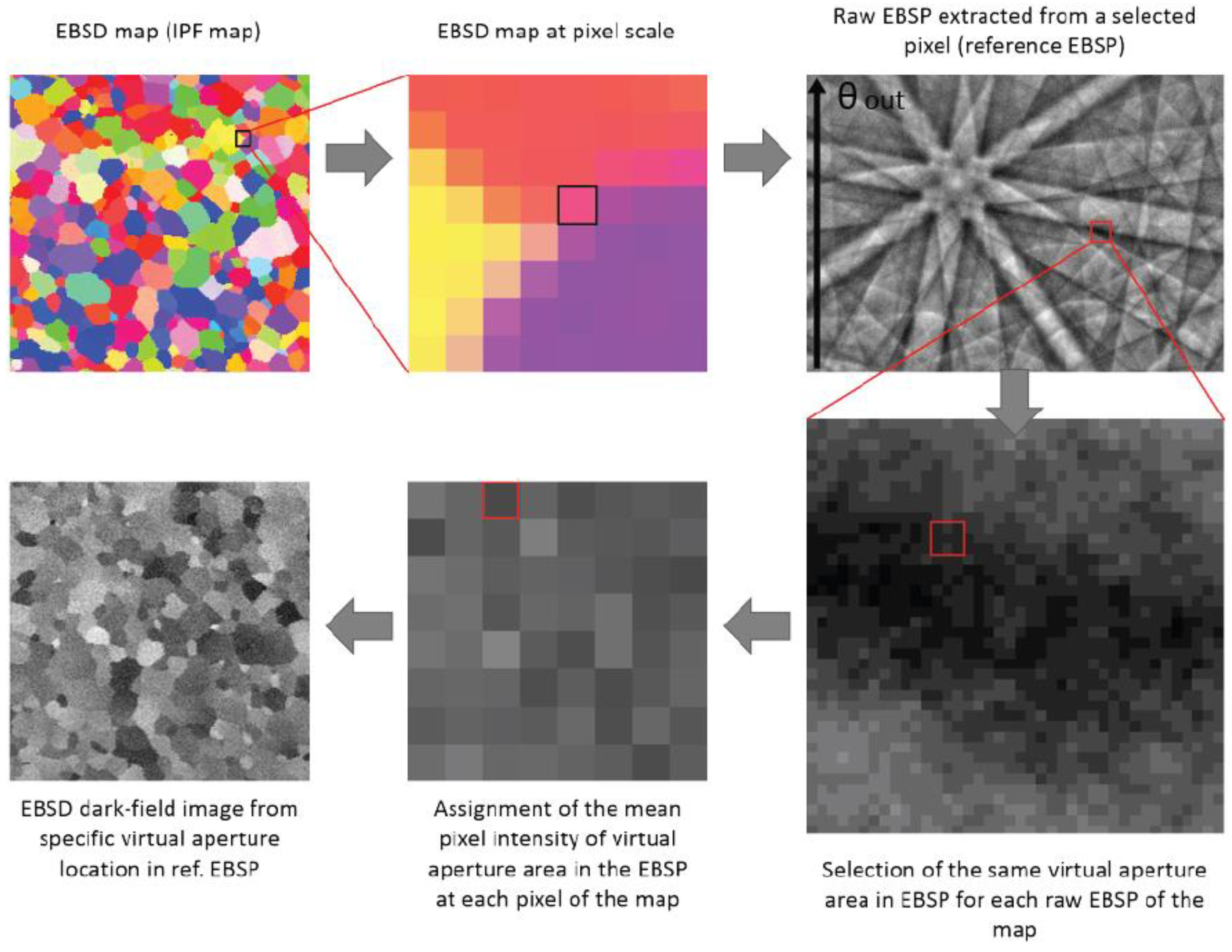
The method originally described by Brodusch et al. was inspired by the contrast mechanism of ECCI. In ECCI, the intensity at each pixel of the image is determined by the intensity at the center of the ECP, which corresponds to the optic axis of the SEM [32]. When the local orientation changes, a shift of the ECP is observed, and the intensity at the optic axis point of the ECP, modulated by its angular resolution, changes. In our technique, a dataset of EBSPs is first acquired and stored. Then, a reference EBSP is chosen from a specific location in the original EBSD map and an array of pixels or a single pixel is selected on that reference pattern. The intensity is summed over the reference EBSP’s pixel array and assigned to the pixel in the reconstructed map (EBSD map). This procedure is repeated for each pixel of the original map, and the resulting reconstructed map is named EBSD-DF image. Thus, the pixel array in the reference image acts as a virtual beam or a virtual aperture similar to that used for dark-field imaging in the TEM. The procedure described above is illustrated in Figure 3. Note that for convention, the term EBSP will be used throughout the text as a reference to the image collected by the EBSD camera, even if it does not contain any Kikuchi lines. It is important to note that our method gathers a lot of information on a specific sample area with only one scan, but is mostly intended to help the SEM user to optimize the collection angles of the BSE detector (the forward scatter detector, FSD, in highly tilted condition) and to position the EBSD camera accurately to maximize the image contrasts obtained with the FSD detector.
A program capable of reprocessing the EBSD dataset was developed, based on the Python programming language (https://python.org), and is available via the repository hosting service platform Bitbucket (https://bitbucket.org) at the address https://bitbucket.org/brodusch/py_ebsd_df. To accelerate the access and processing of the dataset, the stored EBSPs are first transferred into an hdf5 file (https://support.hdfgroup.org) in the form of a datacube. To generate the EBSD-DF images, the array of pixels is selected by the user, and EBSD-DF images can be saved if necessary.
3. Results
3.1. EBSD-Dark-Field Imaging
Originally, the EBSD-DF method was developed to generate images for which the contrast was clearly related to the diffraction reflection selected [16,17], thus generating a large number of ECCI-like images from a single scan. This application essentially holds for single orientation areas where only slight deviations from the selected diffraction condition will produce interpretable contrast, similarly to ECCI. This resulted in a better description of the microstructure of the specimen, especially where complex deformation structures were expected, like those surrounding micro- and nano-indents. It has to be noted that in order to obtain a similar set of images from conventional ECCI analyses, one would need to rotate and tilt the specimen (or the beam) to generate a new image for each specific diffraction condition, and this, hundreds of times. This would be time consuming and is not realistic.
In addition to this, we demonstrated the capability of this new technique to simulate ECCI contrast with known conditions to improve the understanding of the contrasts observed when performing an ECCI analysis. The similarity between the ECCI and EBSD-DF images as shown in [31] confirmed that the primary assumption at the origin of the method was appropriate, and that the results obtained by applying the EBSD-DF technique could be transferred to ECCI. Work is in progress on this subject, and will be reported in a separate publication.
3.2. Compositional Imaging
It is known that the collection angle sustained by a BSE detector influences the contrast of the resulting BSE image, as recently reported by Aoyama and co-workers [33,34]. The raw signal collected by an EBSD detector reflects the angular distribution of the backscattered and forwarded electrons from a highly tilted specimen under electron bombardment. Wells et al. [11] first reported the impact of the collection area on the image obtained when the EBSD detector was used to generate an image. Here we used a specimen containing several distinct phases to evidence the main differences in terms of contrast regarding the position of the pixel array on the EBSD screen plane.
In order to study the impact of the angular distribution of BSEs on compositional contrast, a sample consisting of several mineral phases was investigated. To describe the chemistry of the sample, qualitative EDS background subtracted (net intensity) X-ray images were recorded, and are displayed in Figure 4 for elements S, Fe, Zn, and Pb. As shown, this specimen was mainly composed of sulfide phases. The dark areas in all maps at the same location were considered to be porosity.
Figure 5 presents reconstructed images of the same sample but from a different area, with specific collection areas in the reference image using the procedure described in Section 2.3. For each image, the inset shows the reference image captured via the EBSD detector with the collection area defined by the white square. Due to the limited detector distance achievable with our system, the BSE angular distribution was not totally captured by the EBSD camera. However, the extent of angular distribution collected by this system still allows one to draw useful conclusions. The image displayed in Figure 5a was obtained when the intensity from the full area of the camera screen was collected, i.e., without angular filtration. The contrast observed is typical of compositional contrast, and the major phases identified in Figure 4 are easily recognized. When only a small pixel array around the maximum of intensity of the reference image was selected (Figure 5b), a loss of contrast was noted, although it did not prevent the different phases from being properly identified. However, when comparing images obtained by collecting pixel arrays from the top (Figure 5c) and bottom (Figure 5d) center areas of the reference image, the change in contrast was more striking. Indeed, the contrast obtained with BSEs emitted towards the top of the EBSD camera screen, i.e., with high θout angles, produced a dramatic increase of compositional contrast, while the image obtained by collecting low θout exit angles exhibited a very weak compositional contrast. However, when low emission angles (θout) were collected (Figure 5d), the surface topography became more pronounced, eventually hiding compositional details such as those inside the large pore observed in the center bottom left of the image. The topography observed at the surface of this specimen was expected, and is an artefact of the flat ion milling technique that was applied to the specimen prior to the EBSD acquisition. In addition, a contrast inversion can be noticed between the dark (pyrite, FeS2) and the bright (galena, PbS) phases when switching from low to high emission angles (θout). To our knowledge, this inversion has never been reported in the literature using this set-up. Inversion of Z-contrast was reported recently by Aoyama and co-workers [34], but only at low beam energy and with a 0° specimen tilt set-up and a solid-state BSE detector. This type of inversion might be mostly due to some surface contamination. However, in our experiment, high beam energy was used, thus greatly reducing the effect of surface contamination, even with a high-tilt set-up. Flat milling was applied to the specimen to reduce the contamination artefacts due to surface contaminants as much as possible.
When comparing images obtained with pixel arrays from the center left (Figure 5e) and right (Figure 5f) areas of the reference image, no significant change of contrast could be observed; only the illumination intensity due to a slight shift between the two positions regarding the maximum intensity position. Also, one may notice that the contrast from these two images was similar to that of the image obtained from the central position (Figure 5b). Based on this finding, large azimuthal collection angles were used to generate the images shown in Figure 6, while the angle along the y-axis of the reference image was kept similar to that in Figure 5b–d. This allowed us to reduce statistical noise and increase the visibility on the compositional contrast inversion, in addition to compensating for the illumination variation along the camera x-axis observed in Figure 5e–f.
3.3. Magnetic Domain Imaging
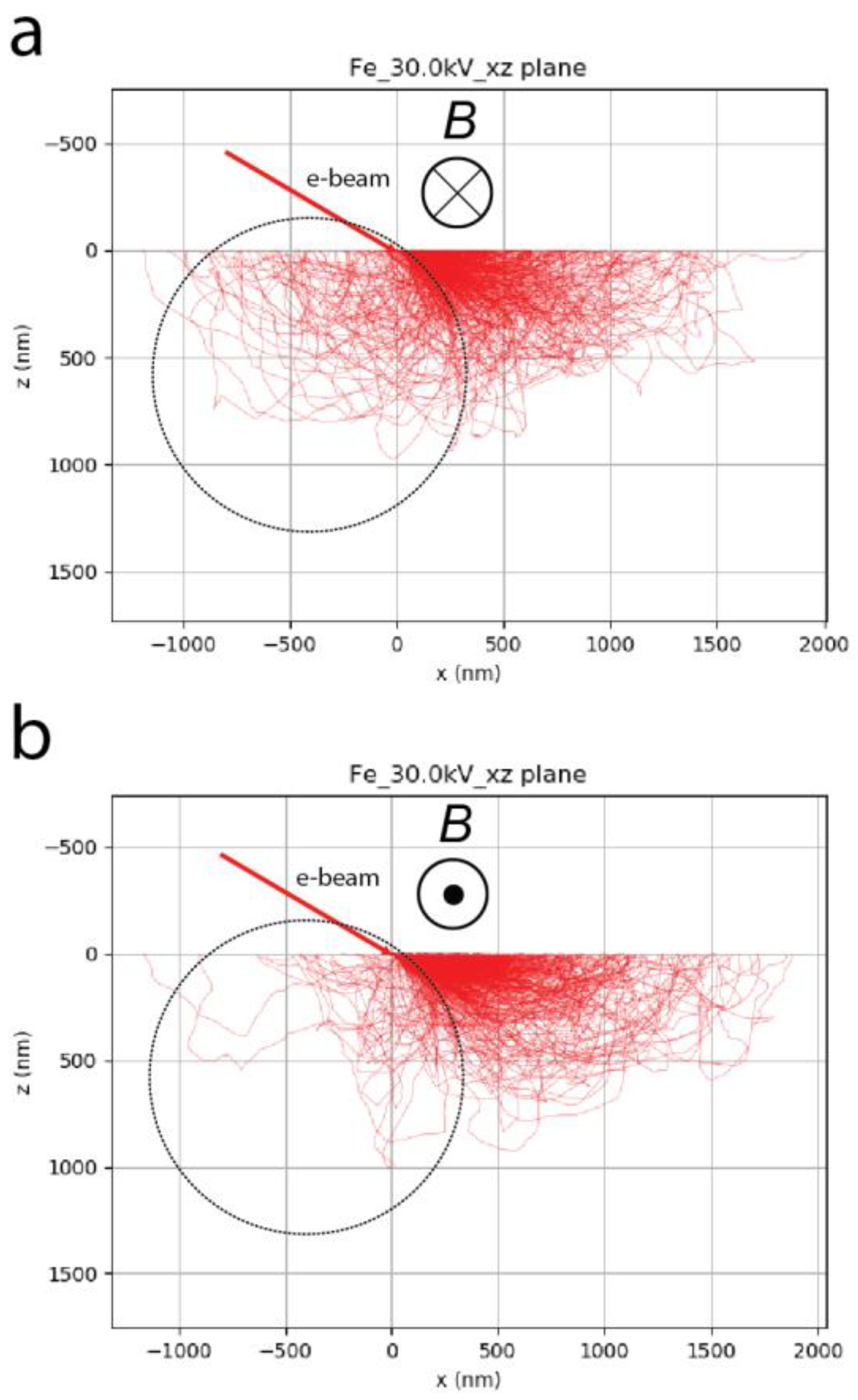
There are several ways to image the magnetic domain structures of ferro-magnetic materials like iron, cobalt, nickel, and their alloys, as well as manganese alloys. A review of these techniques is available in [2]. While contrast of type I is observed due to stray fields generated by the domains above the specimen surface [35,36], the closed magnetic domains from a polished surface can be imaged with magnetic contrast of type II [37,38]. This contrast arises because of the interaction of the internal magnetic field of the specimen with the beam electrons diffusing through the specimen. In fact, maximum contrast between domains of opposite magnetization is obtained when the magnetic field vector, , is parallel to the tilt axis of the microscope and the specimen titled to 50–70° [26,27]. The Lorentz force applied to each primary electron inside the specimen deviates its path inward (Figure 7a) or outward (Figure 7b) the exit surface, depending on the direction of , compared to a situation without magnetic force. This mechanism modulates the BSE yield captured by the BSE detector for each opposite domain.
Recently, there has been a renewed interest in magnetic domain imaging using contrast of type II, because the optimum specimen tilt and beam energy conditions are similar to those necessary for analyzing crystal orientation by conventional EBSD. The combination of these two techniques makes it possible to relate the observed specific magnetic domain structures with the angles between the specimen surface and the closest easy axis of each grain [28]. This was accomplished without specialized equipment; only an EBSD camera equipped with a set of two solid-state diodes (left side of Figure 8a), known as the forward scatter detector, were necessary. However, although Monte Carlo modeling did reveal the overall mechanisms of production of this contrast more than 40 years ago, optimization of the detection set-up has still not been reported. To this end, we applied the method described above to acquire a set of EBSPs with a single EBSD scan over five magnetic domains from a NOES sample previously located using the FSD attached to the EBSD camera screen (right side of Figure 8a). The EBSPs were recorded with an image resolution of 128 pixels × 96 pixels and no background correction applied, i.e., only raw patterns were recorded. The pixel dwell time and probe current were carefully optimized to avoid saturation of the phosphorescent screen.
The images resulting from using the whole screen area (Figure 8b) and only a small squared area around the maximum of intensity (Figure 8c) are displayed in Figure 8. Note that the Kikuchi bands are clearly visible on the EBSPs even without a background subtraction procedure. These images correspond to the same specimen area as previously imaged with the FSD and given in Figure 8a. Obviously, both images provide a similar contrast C as indicated on each image, i.e., 0.123 (Figure 8b) and 0.122 (Figure 8c). The contrast was calculated with the integrated intensities from the two areas indicated in Figure 8a by the black rectangles. Note that the contrasts reported here are of the same order as those reported previously in the literature [27].
As in the case of compositional contrast studied in Section 3.2, small squared pixel arrays were integrated at different locations of the captured EBSP image. The resulting reconstructed images are shown in Figure 9, with the domain images on the right side and the reference EBSP image on the left side with the pixel array defined by the white squares. Contrast values between the domains of opposite magnetization obtained from Equation (1) are given for each domain image. The areas integrated to compute the contrast were identical to those indicated in Figure 8a. Clearly, the location of the collected area on the EBSP image had a dramatic effect on the final domain images. As stated in Section 3.2 regarding the compositional contrast, the polar angle (along the y-axis of the EBSP image) modulates the level of contrast on the domain images. When the top array was collected, the contrast dropped to 0.047 compared to 0.122 obtained with the array centered on the maximum illumination area. This value indicates that the domains become barely visible when high emission angles are collected. In contrast, the image obtained with the collection array located at the bottom of the reference image, i.e., below the maximum of intensity, showed a higher contrast value at 0.166, which expresses an approximate relative increase of contrast of 36%. This indicates that low polar angles should be used to collect the BSE signal in order to maximize magnetic domain contrast of BSE images.
This finding was clearly reproduced when the same pixel array locations were used but shifted to the left or right sides of the reference image (along the x-axis of the image). It must be noted that, due to the extreme locations of the boxes on the left and right positions, non-uniform illumination was observed between the left and right sides of the reconstructed images. Thus, because the contrast was calculated between the central domain and that sitting on its right (Figure 8a), the contrasts values calculated for the images on the right side of Figure 9 were lower than those at the right side of the figure. Although the contrasts values were slightly different for the reason described above, the effect of changing the position of the pixel array along the x-axis of the reference image had a negligible visual effect on the observed contrast.
3.4. EBSD-Dark-Field Applied to Transmission Electron Forward Scattering Diffraction
Transmission EBSD (t-EBSD, t-EFSD, TKD) is an emerging technique and was first reported by Keller and co-workers [39]. It uses a commercial EBSD camera to collect the transmitted diffracted electrons to produce transmission Kikuchi patterns [39,40,41]. This technique is capable of using the full EBSD data processing capabilities on thin electron transparent specimens, in addition to dramatically improving the spatial resolution of orientation mapping to values directly comparable with those obtained with a transmission electron microscope (TEM) [21,22,42,43]. However, the data collected using this technique has not been utilized to its real potential, since most of the work reported so far was concentrated on acquiring orientation or phase maps.
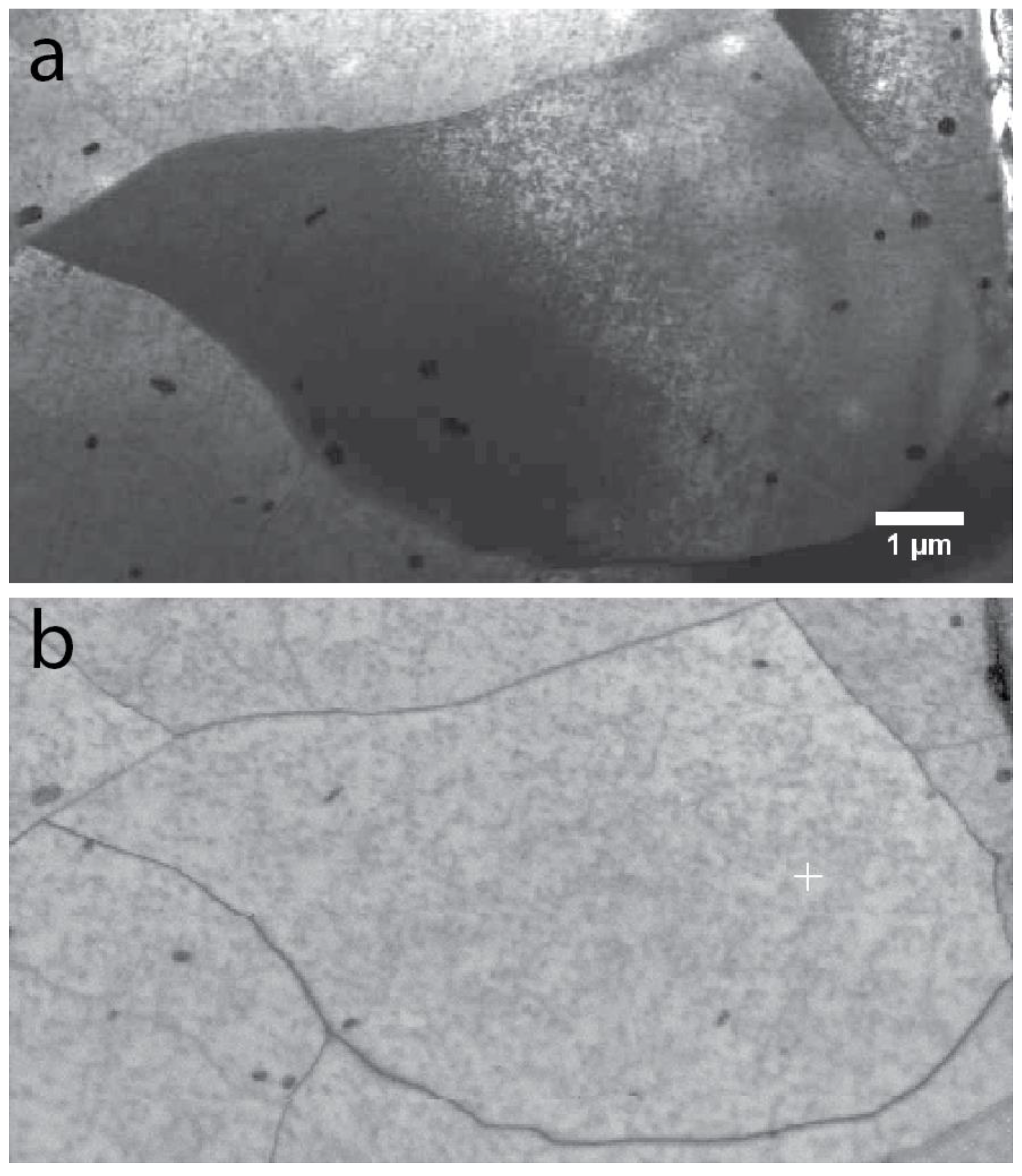
In this section, we report on some preliminary work regarding the use of the EBSD-DF technique to extract useful images from a t-EBSD dataset. A bright-field image recorded using the transmission mode of the SEM, as well as the corresponding band contrast map resulting from a t-EBSD scan on the same area, are shown in Figure 10a,b, respectively. The sample was a thin foil of an AA2099 Al-Li-Cu alloy of approximately 100 nm thickness. The large black precipitates (few hundreds of nm) are Al2Cu, and the very tiny ones are T1 precipitates (50–80 nm), namely Al2CuLi. Note that, possibly due to residual stresses inside some grains that might have been released during the thinning process, the grain in Figure 10 appeared bent, with varying contrast along the grain. Thus, because the T1 precipitates generate a strain field around the precipitates, this allows us to visualize them if a specific diffraction condition is used. The acquisition software was used to produce the band contrast map, and a white cross was marked at the location where the reference pattern displayed in Figure 11 was taken.
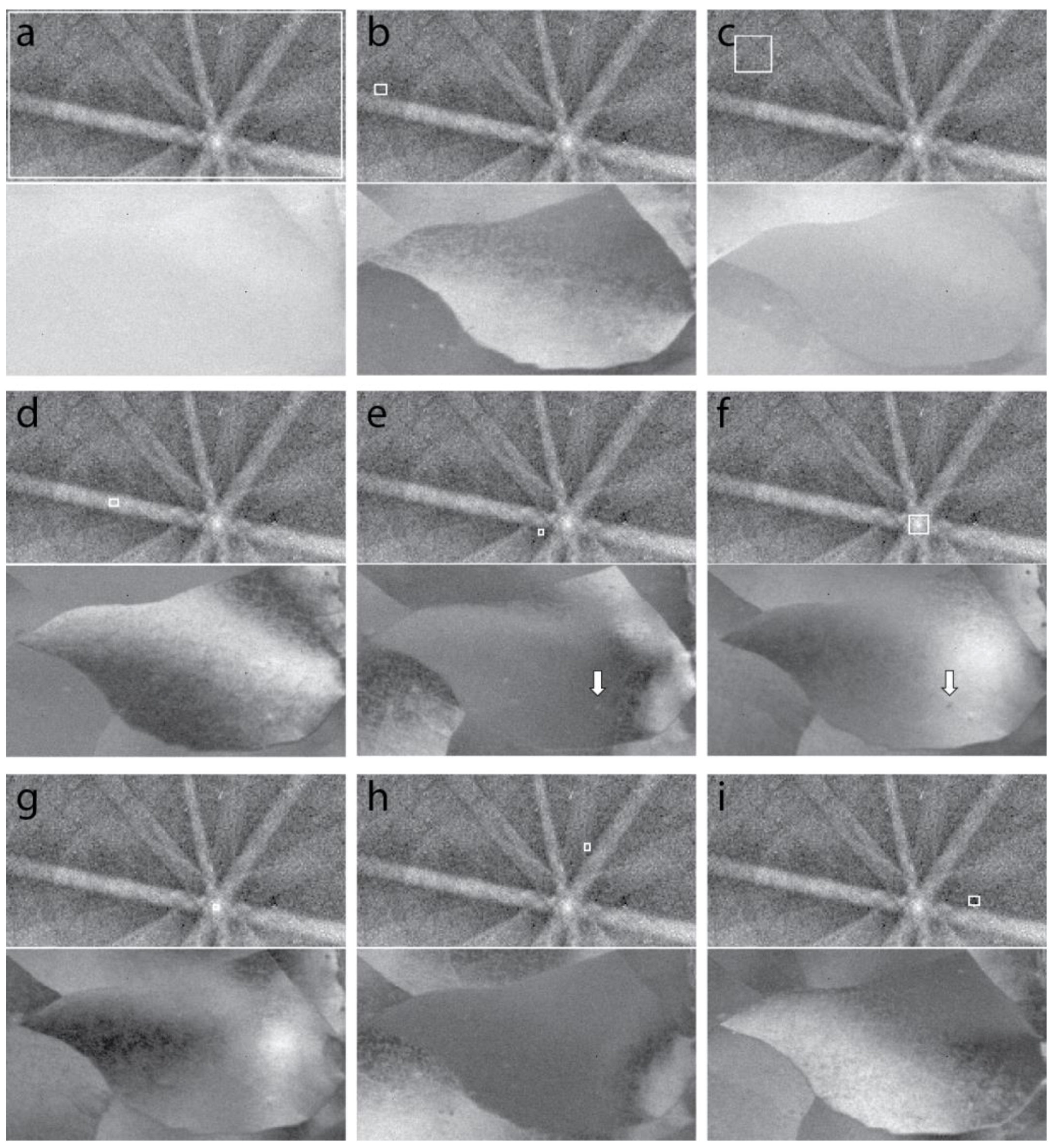
One important characteristic of BF imaging is that the diffraction contrast is predominant for crystalline specimens, which complicates the identification of precipitates by relying only on the Z-contrast. However, when the EBSD-DF technique is applied, different conditions can be tested to obtain many dark-field (DF) images with different contrasts from the same area, allowing us to optimize and better understand the microstructure under investigation. DF images generated from the same set of EBSD data as used in Figure 10 are shown in Figure 11a–i. For each image, the t-EBSP image is given on the top, while the generated DF image is at the bottom. Note that the t-EBSP image was cropped to keep only useful diffraction information, i.e., the region of the camera providing Kikuchi contrast.
When the full t-EBSP area were summed to generate the image in Figure 11a, the contributions from many diffraction conditions were averaged, and the final contrast was very weak, impeding visualization of the true microstructure inside the grain. Similarly, the contrast was very weak when the pixel array was chosen in a region of the t-EBSP with poor Kikuchi band contrast (Figure 11c). On the other hand, if a small sized pixel array was selected in specific areas of the reference pattern, the achievable contrast depended on the specific location chosen. If one looks closely, the intensity at the area where the reference pattern was selected on the reconstructed image (white cross in see Figure 10b) matches the intensity inside of the integrated pixel array in the reference pattern image. For example, when the virtual beam (pixel array) was selected inside a low index zone axis, the zone axis image was observed in the reconstructed image in the same manner as the bend contours in TEM [44] due to the foil bending. This holds also when the virtual beam is positioned inside a Kikuchi band (Figure 11d), where the image of the selected band sits at the location of the reference image. In Figure 11e, the virtual beam is located just in a corner of the zone axis, and consequently, the image of the zone axis appears shifted to the right of the reference pattern position. Note that the contrast is observed here was driven by the crystal rotation due to the foil bending which moved the Kikuchi pattern captured by the EBSD camera around the virtual beam position for every pixel of the grain. It must also be noticed that some precipitates visible in the bright-field image were not observed in any of the reconstructed images in Figure 11. This is due to the depth origin of the diffracted forward scattered electrons captured by the EBSD screen. In fact, the depth resolution of diffracted beams is limited by the inelastic scattering which takes place after the Bragg diffraction events, and thus, only the forward scattered electrons diffracted close to the exit surface are allowed to exit with coherency conservation. This effect must be kept in mind when our method is combined to t-EBSD.
In addition to the bend contour effect, the diffraction conditions used for producing the DF images have a significant influence on the visibility of precipitates in the matrix. Contrast inversion may be observed as in Figure 11, where the two large precipitates at the bottom left of the grain appear either bright on a dark matrix (Figure 11e, see arrow) or dark on a bright matrix (Figure 11f, see arrow). Also, the fine T1 precipitates—that are visible because of the lattice distortions they generate due to the foil bending—were affected by the position of the virtual beam. When a zone axis or the central area of a Kikuchi band are selected, the precipitates are nearly extinguished (Figure 11d,f,g) while they clearly appeared bright over a dark background when the virtual beam was moved to the dark side of the Kikuchi lines (Figure 11e,h,i). This clearly demonstrates the usefulness of the post-processing technique described in this work to better qualify the microstructure of a complex alloy like the one characterized here.
4. Discussion
Its large collection angle, either polar or azimuthal, combined to the pixelization of the collection area make the commercial EBSD camera an ideal device for spatially filtering the backscattered electrons signal emitted from a highly tilted specimen. In addition, the pattern storing and binning facilities of this type of detector makes it efficient in monitoring contrasts over the range of angles collected by the camera, where many images from the same scan can be produced from the exact same specimen area in only one scan. This greatly limits the carbon contamination problems that are often encountered when several scans must be carried out from the exact same region for comparison purposes. With the best cameras currently available, acquisition rates of more than 1000 pattern/s are common, and the latest systems with CMOS technology are capable of acquiring a 1000 × 1000 image in less than 10 min [45]. This means that the time required to record an image becomes comparable to that necessary to record a BSE image with high signal-to-noise ratio. Work in progress on direct detection cameras for EBSD must also be considered, as it might bring a new dimension through energy filtering possibilities provided by this type of detection [46,47].
The experimental results regarding compositional and topographical contrast as a function of the polar collection angle are consistent with previously reported work [9,15,48]. Hence, topographical contrast is enhanced at low θout emission angles. This is due to the increased shadowing on the emitted BSEs at grazing exit angles which are more strongly absorbed than their higher angles counterparts. In addition, these electrons have a limited number of elastic collision in comparison to those emitted at higher angles. In fact, Z-contrast is obtained through the modulation of the emitted intensity depending on Z. At high Z, primary electrons have larger angle elastic collisions, allowing them to reach the surface and be emitted. The primary electrons travelling in a low Z material suffer less large angle elastic collisions, and are thus more absorbed in the matter. The number of emitted BSEs is then lower than that emitted from the high Z material. In high tilt conditions, the number of BSE emitted at small angles (θout) increases due to the reduced path to the surface. However, the BSEs emitted at higher angles suffer more elastic collisions, resulting in larger total deviation (longer path to the surface), and thus, a higher probability of being emitted at a high angle (θout). In consequence, the Z-contrast is stronger at high emission angles. The interesting point that comes out of our experimental results is that compositional contrast inversion was observed at very low angles (30°–40°), even if this contrast was very weak and mostly dominated by topographical contrast. This, to our knowledge, has never been reported, and further work needs to be carried on to confirm this finding. One could suspect channeling contrast as the origin of the contrast inversion, because channeling contrast is stronger at low emission angle. However, the contrast inversion was observed for all grains of the same phase everywhere in the map, and no channeling effects were evidenced. Finally, it must be noted that the azimuthal angle of emission, i.e., the angle around the beam axis, has no effect on the compositional contrast observed with the EBSD detector. This is expected, as the interaction mechanism driving the emission of the BSEs is the same for mirror positions on both sides of the beam impact point as long as the beam is normal to the tilt axis, and no internal magnetic field is present in the specimen.
Magnetic domain imaging was studied in detail more than 40 years ago. The optimum SEM parameters to observe magnetic domain contrast of type II were found to be preferentially high beam accelerating voltage, high specimen tilt, and with the internal magnetic field vector parallel to the tilt axis [27,37,49]. In addition, the contrast between domains is enhanced if energy filtration is applied to the BSE signal, since most of the contrast is carried out by the low-loss BSEs [27,50,51]. However, the effect of the BSE detector collection angles (polar and azimuthal) was not reported, and the preliminary results reported in this work gives new information regarding the understanding of type II magnetic contrast. Hence, the highest contrast was observed at low polar collection angles (θout), meaning a lower angle than that corresponding to the maximum BSE intensity. This suggests that the contrast is maximal when slightly deviated primary electrons are collected, since the bottom area used in Figure 9 (bottom center image) corresponds to collection angles of 30–40° with respect to the specimen surface. According to Wells [50], the low-loss BSEs, mainly responsible for type II contrast, are primary electrons suffering only a single large angle elastic collision, the probability of which decreases with emission angle. The existence of an optimum collection angle for magnetic domain imaging of ferromagnetic materials needs to be confirmed with further experiments and compared with advanced Monte Carlo simulations. The impact of the azimuthal angle also needs to be understood with regard to the internal magnetic field direction, although our results tend to show that it has no effect on our specific example. Thus, by using our approach, the optimum collection parameters for high type II contrast can be determined for any EBSD/FSD system, and this will help in positioning the FSD diodes to get the best contrast. It has to be noted, furthermore, that type II magnetic contrast was reported with 0° tilt angles with a below-the-lens solid state BSE detector on Ni-Mn-Ga alloys, which was not predicted by the simulations performed by Newbury [52,53]. More attention needs to be given to this specific case, and further research on this subject is under way.
The last example that was investigated in Section 3.4 showed the importance of the selected diffraction conditions on the reference EBSP on the resulting images of the microstructure and precipitates. If the summed intensity at the pixel array area of the reference EBSP brings a bright background (BF mode), it may vanish the contrast from lighter precipitates that appear brighter than the matrix if material contrast is considered. On the other hand, if the selected area brings a dark matrix background, the contrast from the same precipitates will be enhanced. The mechanism holds with reversed precipitates contrast. This was demonstrated here with the Al2Cu precipitates with higher mean atomic number compared to the aluminum matrix. This effect has already been reported with the same alloy in bulk form, where BSE imaging at low accelerating voltage was applied with high channeling conditions [54]. In this case, the δ’ Al3Li precipitates were lighter than the Al matrix, but the contrast was found to vary depending on the channeling conditions applied to the Al grain. The same effect was noticed with iron carbides in steel (work not reported). Thus, controlling the background backscattered or transmitted electrons emission in a post-process fashion allows one to monitor precipitates/matrix contrasts, in order to bring a specific area into contrast depending on the area chosen to extract the reference EBSP. This is convenient, especially for deformed materials, where the changing lattice orientation across a grain is detrimental to the extraction of a satisfactory precipitate’s contrast from a single image over the whole grain surface. The availability of a large number of images with different diffraction conditions is capable of resolving the microstructure more finely with only a single scan when our method is applied. This confirms, as already reported for bulk specimens [17], that true DF images in transmission mode can be obtained via this technique where the contrast can be directly related to the diffraction condition used.
5. Conclusions
In this work, an EBSD camera was turned into a BSE detector with a large polar collection angle ranging from around 30° to 100°. Thanks to the storing capability of this equipment, each EBSP image was recorded and stored in a datacube type data set using a dedicated Python program based on the HDF5 export library. Due to the pixelization of the detector frame, the detector captures the BSE angular distribution of the signal emitted from specimens tilted up to 70° with respect to the electron beam, and allows to spatially filter the collected BSE intensity. Thus, for any pixel array selected in the reference EBSP image, a reconstructed image can be produced rapidly by summing the contribution of all the pixels of the array, thanks to the HDF5 datacube format used to store the EBSPs. In this paper, we demonstrated that this large area detector can be successfully used to optimize backscattered or transmitted electrons contrasts of different types; our findings can be summarized as follows:
- In conventional mode, i.e., with highly tilted bulk specimens, our results confirm the previously reported findings regarding the contrast obtained versus the polar collection angle of the camera. High emission angles (θout) with respect to the specimen surface are prone to bring compositional contrast into the reconstructed image, while small emission angles carry the topographic contrast component. However, compositional contrast inversion was found when very small collection angles were collected.
- Magnetic domain contrast imaging at elevated tilt angles was optimized by comparing images obtained at different polar emission angles. The highest contrast was obtained with the BSEs emitted at the lowest angles with respect to the specimen surface. Further investigations need to be carried out to confirm, and maybe improve, the contrast if possible.
- When the reference image captured by the EBSD camera arises from a crystalline material, the reconstructed images carry the diffraction information related to the specific reflection excited via the virtual beam represented by the pixel array chosen in the reference EBSP. The resulting images thus mimics electron channeling contrast, and allows us to visualize deformation in materials in a new way thanks to the many multiple images that can be generated with this technique from a single scan.
- The diffraction contrast was applied to the transmission mode (t-EBSD) and was capable of generating real transmission dark-field images where the contrast relates to the reflection selected in the reference pattern. The impact on the visibility of fine precipitates inside the matrix was demonstrated, and again, the importance of selecting many different reflections from a single scan was shown to be efficient in characterizing the fine microstructure of a material.
The main limitation of our method is the acquisition time of the EBSD dataset necessary to obtain these images after post-processing; this is mainly due to limitations of the EBSD system hardware. However, the new generation of EBSD cameras have fast mapping capabilities, and the development of direct electron detection cameras for EBSD will bring this method to the level of routine application, especially if energy filtration is coupled with the selection of the collection angles.
Finally, thanks to these preliminary and encouraging results presented in this work, future work needs to be carried out to make the method more robust. A study of the intake of big data analysis to reduce the amount of useful data should be carried out. A reflection on different types of shape, and how they could be combined to generate new contrasts, must also be undertaken. The possibility of choosing a uniform emission angle over the EBSD screen is another potential development to allow us to better master contrast.
Author Contributions
N.B, H.D. and R.G.; Methodology, N.B, H.D. and R.G.; Software, N.B, H.D. and R.G.; Validation, N.B, H.D. and R.G.; Formal Analysis, N.B, H.D. and R.G.; Investigation, N.B, H.D. and R.G.; Resources, N.B, H.D. and R.G.; Data Curation, N.B, H.D. and R.G.; Writing—Original Draft Preparation, N.B, H.D. and R.G.; Writing—Review \& Editing, N.B, H.D. and R.G.; Visualization, N.B, H.D. and R.G.; Supervision, R.G.; Project Administration, N.B, H.D. and R.G.; Funding Acquisition, No funding.
Funding
This research received no external funding.
Conflicts of Interest
The authors declare no conflict of interest.
References
- Bell:, D.C.; Erdman, N. Low Voltage Electron Microscopy: Principles and Applications; John Wiley & Sons: Hoboken, NJ, USA, 2012. [Google Scholar]
- Brodusch, N.; Demers, H.; Gauvin, R. Field Emission Scanning Electron Microscopy: New Perspectives for Materials Characterization; Springer: Singapore, 2017; p. 137. [Google Scholar]
- Coates, D.G. Kikuchi-like reflection patterns obtained with the scanning electron microscope. Philos. Mag. 1967, 16, 1179–1184. [Google Scholar] [CrossRef]
- Venables, J.A.; Harland, C.J. Electron back-scattering patterns—A new technique for obtaining crystallographic information in the scanning electron microscope. Philos. Mag. 1973, 27, 1193–1200. [Google Scholar] [CrossRef]
- Schwarzer, R.A.; Field, D.P.; Adams, B.L.; Kumar, M.; Schwartz, A.J. Present state of electron backscatter diffraction and prospective developments. In Electron Backscatter Diffraction in Materials Science; Schwartz, A.J., Kumar, M., Adams, B.L., Field, D.P., Eds.; Springer: Berlin, Germany, 2009; pp. 1–20. [Google Scholar]
- Schwartz, A.J.; Kumar, M.; Adams, B.L.; Field, D.P. Electron Backscatter Diffraction in Materials Science; Springer: Berlin, Germany, 2009. [Google Scholar]
- Zaefferer, S. On the formation mechanisms, spatial resolution and intensity of backscatter kikuchi patterns. Ultramicroscopy 2007, 107, 254–266. [Google Scholar] [CrossRef] [PubMed]
- Steinmetz, D.R.; Zaefferer, S. Towards ultrahigh resolution EBSD by low accelerating voltage. Mater. Sci. Technol. 2010, 26, 640–645. [Google Scholar] [CrossRef]
- Prior, D.J.; Trimby, P.; Weber, U.; Dingley, D.J. Orientation contrast imaging of microstructures in rocks using forescatter detectors in the scanning electron microscope. Miner. Mag. 1996, 60, 859–869. [Google Scholar] [CrossRef]
- Payton, E.J.; Nolze, G. The backscatter electron signal as an additional tool for phase segmentation in electron backscatter diffraction. Microsc. Microanal. 2013, 19, 929–941. [Google Scholar] [CrossRef] [PubMed]
- Wells, O.C.; Gignac, L.M.; Murray, C.E.; Frye, A.; Bruley, J. Use of backscattered electron detector arrays for forming backscattered electron images in the scanning electron microscope. Scanning 2006, 28, 27–31. [Google Scholar] [CrossRef] [PubMed]
- Schwarzer, R.A.; Hjelen, J. Backscattered electron imaging with an EBSD detector. Microsc. Today 2015, 23, 12–17. [Google Scholar] [CrossRef]
- Schwarzer, R.A.; Sukkau, J. Electron back scattered diffraction: Current state, prospects and comparison with X-ray diffraction texture measurement. Banaras Metall. 2013, 18, 1–11. [Google Scholar]
- Nowell, M.M.; Wright, S.I.; Rampton, T.; de Kloe, R. A new microstructural imaging approach through EBSD pattern region of interest analysis. Microsc. Microanal. 2014, 20, 1116–1117. [Google Scholar] [CrossRef]
- Wright, S.I.; Nowell, M.M.; de Kloe, R.; Camus, P.; Rampton, T. Electron imaging with an EBSD detector. Ultramicroscopy 2015, 148, 132–145. [Google Scholar] [CrossRef] [PubMed]
- Brodusch, N.; Demers, H.; Gauvin, R. Dark-field imaging based on post-processing of electron backscatter diffraction patterns in a scanning electron microscope. Microsc. Microanal. 2015, 21, 2031–2032. [Google Scholar] [CrossRef]
- Brodusch, N.; Demers, H.; Gauvin, R. Dark-field imaging based on post-processed electron backscatter diffraction patterns of bulk crystalline materials in a scanning electron microscope. Ultramicroscopy 2015, 148, 123–131. [Google Scholar] [CrossRef] [PubMed]
- Chapman, M.; Callahan, P.; Graef, M. EBSD surface topography determination in a martensitic Au-Cu-Zn alloy. Microsc. Microanal. 2015, 21, 2215–2216. [Google Scholar] [CrossRef]
- Chapman, M.; Callahan, P.G.; De Graef, M. Determination of sample surface topography using electron back-scatter diffraction patterns. Scr. Mater. 2016, 120, 23–26. [Google Scholar] [CrossRef] [Green Version]
- Dorri, M.; Turgeon, S.; Brodusch, N.; Cloutier, M.; Chevallier, P.; Gauvin, R.; Mantovani, D. Characterization of amorphous oxide nano-thick layers on 316l stainless steel by electron channeling contrast imaging and electron backscatter diffraction. Microsc. Microanal. 2016, 22, 997–1006. [Google Scholar] [CrossRef] [PubMed]
- Brodusch, N.; Demers, H.; Gauvin, R. Nanometres-resolution kikuchi patterns from materials science specimens with transmission electron forward scatter diffraction in the scanning electron microscope. J. Microsc. 2013, 250, 1–14. [Google Scholar] [CrossRef] [PubMed]
- Brodusch, N.; Demers, H.; Trudeau, M.; Gauvin, R. Acquisition parameters optimization of a transmission electron forward scatter diffraction system in a cold-field emission scanning electron microscope for nanomaterials characterization. Scanning 2013, 35, 375–386. [Google Scholar] [CrossRef] [PubMed]
- Gauvin, R.; Lifshin, E.; Demers, H.; Horny, P.; Campbell, H. Win X-ray: A new Monte Carlo program that computes X-ray spectra obtained with a scanning electron microscope. Microsc. Microanal. 2006, 12, 49–64. [Google Scholar] [CrossRef] [PubMed]
- Joy, D.C.; Luo, S. An empirical stopping power relationship for low-energy electrons. Scanning 1989, 11, 176–180. [Google Scholar] [CrossRef]
- Heinrich, K.F.; Newbury, D.E.; Yakowitz, H. Use of Monte Carlo Calculations in Electron Probe Microanalysis and Scanning Electron Microscopy: Proceedings of a Workshop Held at the National Bureau of Standards, Gaithersburg, Maryland, October 1–3, 1975; US Dept. of Commerce, National Bureau of Standards: Washington, DC, USA; US Govt. Print. Off.: Washington, DC, USA, 1976.
- Newbury, D.E.; Yakowitz, H.; Myklebust, R.L. Monte carlo calculations of magnetic contrast from cubic materials in the scanning electron microscope. Appl. Phys. Lett. 1973, 23, 488–490. [Google Scholar] [CrossRef]
- Newbury, D.E.; Yakowitz, H.; Myklebust, R.L. A study of type ii magnetic domain contrast in the SEM by Monte Carlo electron trajectory simulation. In Use of Monte Carlo Calculations in Electron Probe Microanalysis and Scanning Electron Microscopy: Proceedings of a Workshop Held at the National Bureau of Standards, Gaithersburg, Maryland, October 1–3, 1975; US Dept. of Commerce, National Bureau of Standards: Washington, DC, USA; US Govt. Print. Off.: Washington, DC, USA, 1976. [Google Scholar]
- Gallaugher, M.; Brodusch, N.; Gauvin, R.; Chromik, R.R. Magnetic domain structure and crystallographic orientation of electrical steels revealed by a forescatter detector and electron backscatter diffraction. Ultramicroscopy 2014, 142, 40–49. [Google Scholar] [CrossRef] [PubMed]
- Reimer, L. Scanning electron microscopy: Physics of image formation and microanalysis. Meas. Sci. Technol. 1998, 11, 1826. [Google Scholar] [CrossRef]
- Wells, O.C. Comparison of different models for the generation of electron backscattering patterns in the scanning electron microscope. Scanning 1999, 21, 368–371. [Google Scholar] [CrossRef]
- Kaboli, S.; Demers, H.; Brodusch, N.; Gauvin, R. Rotation contour contrast reconstruction using electron backscatter diffraction in a scanning electron microscope. J. Appl. Crystallogr. 2015, 48, 776–785. [Google Scholar] [CrossRef]
- Holt, D.B.; Muir, M.D.; Grant, P.R.; Boswarva, I.M. Quantitative Scanning Electron Microscopy; Academic Press: London, UK; New York, NY, USA; San Francisco, CA, USA, 1974. [Google Scholar]
- Aoyama, T.; Nagoshi, M.; Nagano, H.; Sato, K.; Tachibana, S. Selective backscattered electron imaging of material and channeling contrast in microstructures of scale on low carbon steel controlled by accelerating voltage and take-off angle. ISIJ Int. 2011, 51, 1487–1491. [Google Scholar] [CrossRef]
- Aoyama, T.; Nagoshi, M.; Sato, K. Quantitative analysis of angle-selective backscattering electron image of iron oxide and steel. Microscopy 2015, 64, 319–325. [Google Scholar] [CrossRef] [PubMed]
- Banbury, J.R.; Nixon, W.C. The direct observation of domain structure and magnetic fields in the scanning electron microscope. J. Sci. Instrum. 1967, 44, 889. [Google Scholar] [CrossRef]
- Joy, D.C.; Jakubovics, J.P. Direct observation of magnetic domains by scanning electron microscopy. Philos. Mag. 1968, 17, 61–69. [Google Scholar] [CrossRef]
- Fathers, D.J.; Jakubovics, J.P.; Joy, D.C.; Newbury, D.E.; Yakowitz, H. A new method of observing magnetic domains by scanning electron microscopy I. Theory of the image contrast. Phys. Status Solidi A 1973, 20, 535–544. [Google Scholar] [CrossRef]
- Fathers, D.J.; Jakubovics, J.P.; Joy, D.C.; Newbury, D.E.; Yakowitz, H. A new method of observing magnetic domains by scanning electron microscopy. II. Experimental confirmation of the theory of image contrast. Phys. Status Solidi A 1974, 22, 609–619. [Google Scholar] [CrossRef]
- Geiss, R.H.; Keller, R.R.; Read, D.T. Transmission electron diffraction from nanoparticles, nanowires and thin films in an SEM with conventional EBSD equipment. Microsc. Microanal. 2010, 16, 1742–1743. [Google Scholar] [CrossRef]
- Geiss, R.; Keller, R.; Sitzman, S.; Rice, P. New method of transmission electron diffraction to characterize nanomaterials in the sem. Microsc. Microanal. 2011, 17, 386–387. [Google Scholar] [CrossRef]
- Keller, R.; Geiss, R. Transmission ebsd from 10 nm domains in a scanning electron microscope. J. Microsc. 2012, 245, 245–251. [Google Scholar] [CrossRef]
- Suzuki, S. Features of transmission EBSD and its application. JOM 2013, 65, 1254–1263. [Google Scholar] [CrossRef]
- Trimby, P.W. Orientation mapping of nanostructured materials using transmission kikuchi diffraction in the scanning electron microscope. Ultramicroscopy 2012, 120, 16–24. [Google Scholar] [CrossRef] [PubMed]
- Steeds, J.W.; Tatlock, G.J.; Hampson, J. Real space crystallography. Nature 1973, 241, 435. [Google Scholar] [CrossRef]
- Oxford_Instruments. Rapid Characterization of Steel and Ni. Application Note 2017. Available online: http://symmetry.oxford-instruments.com/ (accessed on 1 March 2018).
- Vespucci, S.; Winkelmann, A.; Naresh-Kumar, G.; Mingard, K.P.; Maneuski, D.; Edwards, P.R.; Day, A.P.; O’Shea, V.; Trager-Cowan, C. Digital direct electron imaging of energy-filtered electron backscatter diffraction patterns. Phys. Rev. B 2015, 92, 205301. [Google Scholar] [CrossRef]
- Wilkinson, A.J.; Moldovan, G.; Britton, T.B.; Bewick, A.; Clough, R.; Kirkland, A.I. Direct detection of electron backscatter diffraction patterns. Phys. Rev. Lett. 2013, 111, 065506. [Google Scholar] [CrossRef] [PubMed]
- Reimer, L.; Riepenhausen, M.; Schierjott, M. Signal of backscattered electrons at edges and surface steps in dependence on surface tilt and take-off direction. Scanning 1986, 8, 164–175. [Google Scholar] [CrossRef]
- Yamamoto, T.; Nishizawa, H.; Tsuno, K. Magnetic domain contrast in backscattered electron images obtained with a scanning electron microscope. Philos. Mag. 1976, 34, 311–325. [Google Scholar] [CrossRef]
- Wells, O. Calculation of type ii magnetic contrast in the low-loss image in the scanning electron microscope. In Use of Monte Carlo Calculations in Electron Probe Microanalysis and Scanning Electron Microscopy: Proceedings of a Workshop Held at the National Bureau of Standards, Gaithersburg, Maryland, October 1–3, 1975; US Dept. of Commerce, National Bureau of Standards: Washington, DC, USA; US Govt. Print. Off.: Washington, DC, USA, 1976. [Google Scholar]
- Wells, O.C.; Savoy, R.J. Enhancement of type-2 magnetic contrast in the BSE image in the SEM by a lock-in technique. Scanning 1979, 2, 255–256. [Google Scholar] [CrossRef]
- Ge, Y.; Heczko, O.; Soderberg, O.; Hannula, S.P.; Lindroos, V.K. Investigation of magnetic domains in Ni–Mn–Ga alloys with a scanning electron microscope. Smart Mater. Struct. 2005, 14, S211. [Google Scholar] [CrossRef]
- Ge, Y.; Heczko, O.; Soderberg, O.; Lindroos, V. Various magnetic domain structures in a Ni-Mn-Ga martensite exhibiting magnetic shape memory effect. J. Appl. Phys. 2004, 96, 2159–2163. [Google Scholar] [CrossRef]
- Brodusch, N.; Voisard, F.; Gauvin, R. About the contrast of δ’ precipitates in bulk Al-Cu-Li alloys in reflection mode with a field-emission scanning electron microscope at low accelerating voltage. J. Microsc. 2017, 268, 107–118. [Google Scholar] [CrossRef] [PubMed]
Figure 1.
Schematics describing (a) the conventional electron backscattered diffraction (EBSD) set-up and (b) the transmission EBSD (t-EBSD) set-up; (c) Calibration relating the BSE emission angle θout and the distance L from the bottom of the EBSD camera screen. SINGLE COLUMN.
Figure 1.
Schematics describing (a) the conventional electron backscattered diffraction (EBSD) set-up and (b) the transmission EBSD (t-EBSD) set-up; (c) Calibration relating the BSE emission angle θout and the distance L from the bottom of the EBSD camera screen. SINGLE COLUMN.

Figure 2.
Typical pseudo-Kikuchi pattern obtained in a scanning electron microscope with (a) the electron backscattered diffraction (EBSP) technique and (b) the electron channeling technique (ECP) on a (001) oriented LaAlO3 single crystal. Accelerating voltage was 20 kV in (a) and 30 kV in (b). Note the level of detail available in the (001) zone axis displayed in (b). SINGLE COLUMN.

Figure 3.
Description of the procedure to obtain post-processed EBSD-DF images from a stored EBSD dataset. DOUBLE COLUMN.
Figure 3.
Description of the procedure to obtain post-processed EBSD-DF images from a stored EBSD dataset. DOUBLE COLUMN.

Figure 4.
EDS net intensity maps with the corresponding SE image from the galena-rich slag obtained with an accelerating voltage of 5 kV showing that the slag was essentially constituted of iron sulfide, zinc sulfide and lead sulfide. The scalebar displayed on the SE image applies to the corresponding X-ray images. SINGLE COLUMN.

Figure 5.
Reconstructed images from an EBSD scan at E0 = 20 kV acquired from a mineral slag sample with the pixel array areas on the reference image (inset) as highlighted by the white squares. (a) Full reference image area; (b) small area at the center; (c) small area from top-center; (d) small area from bottom-center; (e) small area from left-center and (f) small area from right-center. The scalebar displayed on the image (a) applies to all the other images of the figure. DOUBLE COLUMN.

Figure 6.
Reconstructed images from the same EBSD scan as in Figure 5. The white rectangles in the reference image shown in the inset define the pixel arrays integrated to obtain each image. (a) Top; (b) center and (c) bottom region of the EBSD camera. The scalebar displayed on the image in Figure 5a applies to all the reconstructed images of this figure.

Figure 7.
Monte Carlo simulations of electron trajectories in pure iron with 2000 trajectories displayed with the internal magnetic field vector parallel to the tilt axis pointing in the direction into (a) and out of (b) the plane of the figure. Tilt angle was 70° as in a conventional EBSD set-up. The strength of the magnetic induction was deliberately set to 100 T to enhance the magnetic deflection for ease of visualization. The deflection effect of the internal magnetic field of the specimen is clearly seen in the region indicated by the black dotted circles.

Figure 8.
Magnetic domain images obtained from a non-oriented Fe-2.78%-Si electrical steel (right) and collection areas used to produce the images (left) with (a) the forward scatter detector (diode 1 + diode 2) attached to the EBSD camera screen; (b) the summed intensities over the full area of the EBSD camera screen and (c) the summed intensities from a small rectangle located around the maximum illumination area. The black rectangles in (a) define the areas used to calculate the contrast C displayed in (b–c). The scale bar displayed on the FSD image in (a) applies to the images in (b–c).

Figure 9.
Magnetic domain images (right) obtained from the same EBSD scan as Figure 8. The reference image is displayed on the left of each domain image with the white square defining the collection area used for the image reconstruction. The scalebar displayed on the FSD image in Figure 8a applies to all the images of the figure.

Figure 10.
(a) Bright-field image of an AA2099 Al-Li-Cu alloy using the transmission mode of the SEM; (b) Band contrast (BC) image corresponding to the same area by transmission EBSD. The white cross locates the position of the reference EBSP used for pixel array selection for the reconstruction of the EBSD-DF images. The scalebar displayed on the STEM image in (a) applies to the BC image in (b).

Figure 11.
(a–i) EBSD-DF images obtained after collecting the intensities from the pixel arrays (virtual beam) defined by the white squares in the reference Kikuchi pattern (t-EBSP). The top and bottom images correspond to the reference pattern and the EBSD-DF image. The white arrows indicate the precipitates affected by the diffraction condition used (see text for more information). Note that the t-EBSPs were background subtracted to enhance diffraction contrast. The scalebar displayed on the STEM image in Figure 9a applies to all reconstructed images this figure.
© 2018 by the authors. Licensee MDPI, Basel, Switzerland. This article is an open access article distributed under the terms and conditions of the Creative Commons Attribution (CC BY) license (http://creativecommons.org/licenses/by/4.0/).
Share and Cite
MDPI and ACS Style
Brodusch, N.; Demers, H.; Gauvin, R. Imaging with a Commercial Electron Backscatter Diffraction (EBSD) Camera in a Scanning Electron Microscope: A Review. J. Imaging 2018, 4, 88. https://doi.org/10.3390/jimaging4070088
AMA Style
Brodusch N, Demers H, Gauvin R. Imaging with a Commercial Electron Backscatter Diffraction (EBSD) Camera in a Scanning Electron Microscope: A Review. Journal of Imaging. 2018; 4(7):88. https://doi.org/10.3390/jimaging4070088
Chicago/Turabian StyleBrodusch, Nicolas, Hendrix Demers, and Raynald Gauvin. 2018. "Imaging with a Commercial Electron Backscatter Diffraction (EBSD) Camera in a Scanning Electron Microscope: A Review" Journal of Imaging 4, no. 7: 88. https://doi.org/10.3390/jimaging4070088
Note that from the first issue of 2016, this journal uses article numbers instead of page numbers. See further details here.